Embed Size (px)
Citation preview
PAANTENNA
RFIN OUT
RF
VDD
GND
50 :
ADC
B1
A1
A2
B2, C1
COUPLER
LMH2110
C2EN
2.4
2.0
1.6
1.2
0.8
0.4
0.0-40 -30 -20 -10 0 10
85°C
-40°C25°C
ER
RO
R (
dB)
RF INPUT POWER (dBm)
VO
UT (
V)
3
2
1
0
-1
-2
-3
Product
Folder
Sample &Buy
Technical
Documents
Tools &
Software
Support &Community
LMH2110SNWS022D –JANUARY 2010–REVISED JUNE 2015
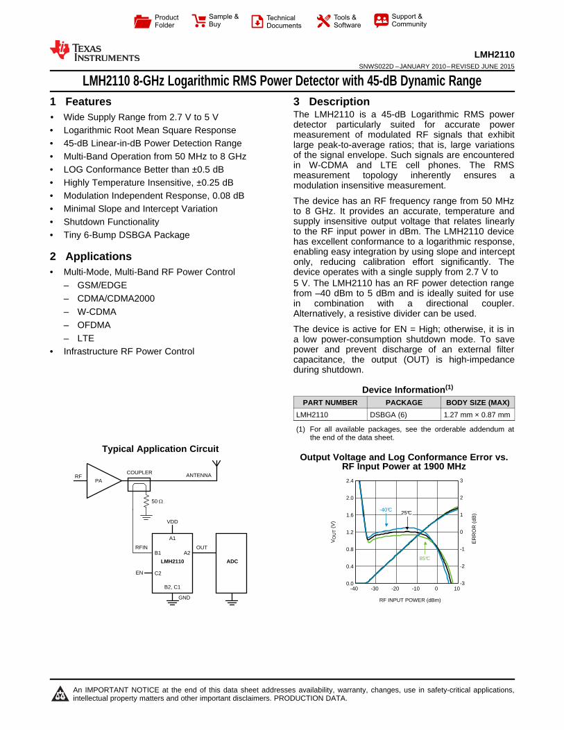
LMH2110 8-GHz Logarithmic RMS Power Detector with 45-dB Dynamic Range1 Features 3 Description
The LMH2110 is a 45-dB Logarithmic RMS power1• Wide Supply Range from 2.7 V to 5 V
detector particularly suited for accurate power• Logarithmic Root Mean Square Response measurement of modulated RF signals that exhibit• 45-dB Linear-in-dB Power Detection Range large peak-to-average ratios; that is, large variations
of the signal envelope. Such signals are encountered• Multi-Band Operation from 50 MHz to 8 GHzin W-CDMA and LTE cell phones. The RMS• LOG Conformance Better than ±0.5 dB measurement topology inherently ensures a
• Highly Temperature Insensitive, ±0.25 dB modulation insensitive measurement.• Modulation Independent Response, 0.08 dB The device has an RF frequency range from 50 MHz• Minimal Slope and Intercept Variation to 8 GHz. It provides an accurate, temperature and
supply insensitive output voltage that relates linearly• Shutdown Functionalityto the RF input power in dBm. The LMH2110 device• Tiny 6-Bump DSBGA Packagehas excellent conformance to a logarithmic response,enabling easy integration by using slope and intercept2 Applications only, reducing calibration effort significantly. The
• Multi-Mode, Multi-Band RF Power Control device operates with a single supply from 2.7 V to5 V. The LMH2110 has an RF power detection range– GSM/EDGEfrom –40 dBm to 5 dBm and is ideally suited for use– CDMA/CDMA2000 in combination with a directional coupler.
– W-CDMA Alternatively, a resistive divider can be used.– OFDMA The device is active for EN = High; otherwise, it is in– LTE a low power-consumption shutdown mode. To save
power and prevent discharge of an external filter• Infrastructure RF Power Controlcapacitance, the output (OUT) is high-impedancespace during shutdown.
Device Information(1)
PART NUMBER PACKAGE BODY SIZE (MAX)LMH2110 DSBGA (6) 1.27 mm × 0.87 mm
(1) For all available packages, see the orderable addendum atthe end of the data sheet.
Typical Application CircuitOutput Voltage and Log Conformance Error vs.
RF Input Power at 1900 MHz
1
An IMPORTANT NOTICE at the end of this data sheet addresses availability, warranty, changes, use in safety-critical applications,intellectual property matters and other important disclaimers. PRODUCTION DATA.
LMH2110SNWS022D –JANUARY 2010–REVISED JUNE 2015 www.ti.com
Table of Contents7.3 Feature Description................................................. 161 Features .................................................................. 17.4 Device Functional Modes........................................ 202 Applications ........................................................... 1
8 Application and Implementation ........................ 213 Description ............................................................. 18.1 Application Information............................................ 214 Revision History..................................................... 28.2 Typical Applications ................................................ 215 Pin Configuration and Functions ......................... 3
9 Power Supply Recommendations ...................... 296 Specifications......................................................... 410 Layout................................................................... 296.1 Absolute Maximum Ratings ...................................... 4
10.1 Layout Guidelines ................................................. 296.2 ESD Ratings.............................................................. 410.2 Layout Example .................................................... 296.3 Recommended Operating Conditions....................... 4
11 Device and Documentation Support ................. 306.4 Thermal Information .................................................. 411.1 Community Resources.......................................... 306.5 2.7-V and 4.5-V DC and AC Electrical
Characteristics ........................................................... 5 11.2 Trademarks ........................................................... 306.6 Timing Requirements ................................................ 8 11.3 Electrostatic Discharge Caution............................ 306.7 Typical Characteristics .............................................. 9 11.4 Glossary ................................................................ 30
7 Detailed Description ............................................ 16 12 Mechanical, Packaging, and OrderableInformation ........................................................... 307.1 Overview ................................................................. 16
7.2 Functional Block Diagram ....................................... 16
4 Revision HistoryNOTE: Page numbers for previous revisions may differ from page numbers in the current version.
Changes from Revision C (March 2013) to Revision D Page
• Added Pin Configuration and Functions section, ESD Ratings table, Feature Description section, Device FunctionalModes, Application and Implementation section, Power Supply Recommendations section, Layout section, Deviceand Documentation Support section, and Mechanical, Packaging, and Orderable Information section .............................. 1
Changes from Revision B (October 2013) to Revision C Page
• Changed layout of National Data Sheet to TI format ........................................................................................................... 29
2 Submit Documentation Feedback Copyright © 2010–2015, Texas Instruments Incorporated
Product Folder Links: LMH2110
OUT
GND
RFIN
VDD A1 A2
B1 B2
C1 C2
GND
EN
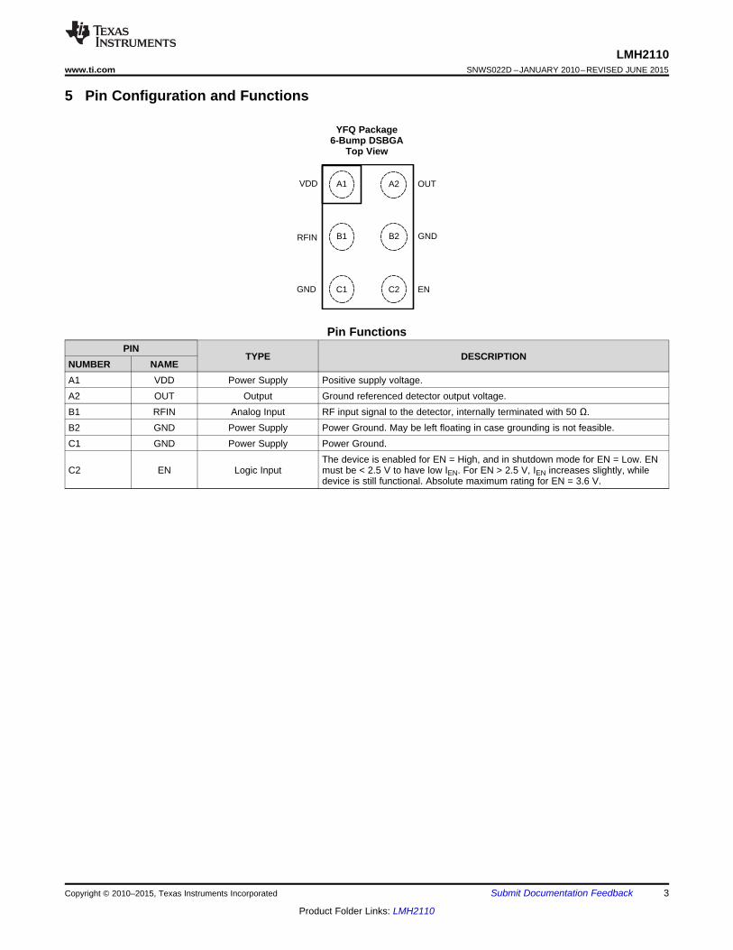
LMH2110www.ti.com SNWS022D –JANUARY 2010–REVISED JUNE 2015
5 Pin Configuration and Functions
YFQ Package6-Bump DSBGA
Top View
Pin FunctionsPIN
TYPE DESCRIPTIONNUMBER NAMEA1 VDD Power Supply Positive supply voltage.A2 OUT Output Ground referenced detector output voltage.B1 RFIN Analog Input RF input signal to the detector, internally terminated with 50 Ω.B2 GND Power Supply Power Ground. May be left floating in case grounding is not feasible.C1 GND Power Supply Power Ground.
The device is enabled for EN = High, and in shutdown mode for EN = Low. ENC2 EN Logic Input must be < 2.5 V to have low IEN. For EN > 2.5 V, IEN increases slightly, while
device is still functional. Absolute maximum rating for EN = 3.6 V.
Copyright © 2010–2015, Texas Instruments Incorporated Submit Documentation Feedback 3
Product Folder Links: LMH2110
LMH2110SNWS022D –JANUARY 2010–REVISED JUNE 2015 www.ti.com
6 Specifications
6.1 Absolute Maximum Ratingsover operating free-air temperature range (unless otherwise noted) (1) (2)
MIN MAX UNITSupply voltage VBAT – GND 5.5 V
Input power 12 dBmRF input
DC voltage 1 VEnable input voltage GND – 0.4 < VEN and VEN< Min (VDD – 0.4 V, 3.6 V)Junction temperature (3) 150 °CMaximum lead temperature (Soldering,10 sec) 260 °CStorage temperature, Tstg −65 150 °C
(1) Stresses beyond those listed under Absolute Maximum Ratings may cause permanent damage to the device. These are stress ratingsonly, which do not imply functional operation of the device at these or any other conditions beyond those indicated under RecommendedOperating Conditions. Exposure to absolute-maximum-rated conditions for extended periods may affect device reliability.
(2) If Military/Aerospace specified devices are required, contact the Texas Instruments Sales Office/ Distributors for availability andspecifications.
(3) The maximum power dissipation is a function of TJ(MAX), RθJA. The maximum allowable power dissipation at any ambient temperature isPD = (TJ(MAX) – TA)/RθJA. All numbers apply for packages soldered directly into a PC board.
6.2 ESD RatingsVALUE UNIT
Human-body model (HBM), per ANSI/ESDA/JEDEC JS-001 (1) ±2000ElectrostaticV(ESD) Charged-device model (CDM), per JEDEC specification JESD22-C101 (2) ±1000 Vdischarge
Machine Model ±200
(1) JEDEC document JEP155 states that 500-V HBM allows safe manufacturing with a standard ESD control process.(2) JEDEC document JEP157 states that 250-V CDM allows safe manufacturing with a standard ESD control process.
6.3 Recommended Operating Conditionsover operating free-air temperature range (unless otherwise noted) (1)
MIN MAX UNITSupply voltage 2.7 5 VOperating temperature −40 85 °CRF frequency 50 8000 MHzRF input power −40 5 dBm
(1) Stresses beyond those listed under Absolute Maximum Ratings may cause permanent damage to the device. These are stress ratingsonly, which do not imply functional operation of the device at these or any other conditions beyond those indicated under RecommendedOperating Conditions. Exposure to absolute-maximum-rated conditions for extended periods may affect device reliability.
6.4 Thermal InformationLMH2110
THERMAL METRIC (1) YFQ (DSBGA) UNIT6 PINS
RθJA Junction-to-ambient thermal resistance 133.7 °C/WRθJC(top) Junction-to-case (top) thermal resistance 1.7 °C/WRθJB Junction-to-board thermal resistance 22.6 °C/WψJT Junction-to-top characterization parameter 5.7 °C/WψJB Junction-to-board characterization parameter 22.2 °C/W
(1) For more information about traditional and new thermal metrics, see the Semiconductor and IC Package Thermal Metrics applicationreport, SPRA953.
4 Submit Documentation Feedback Copyright © 2010–2015, Texas Instruments Incorporated
Product Folder Links: LMH2110
LMH2110www.ti.com SNWS022D –JANUARY 2010–REVISED JUNE 2015
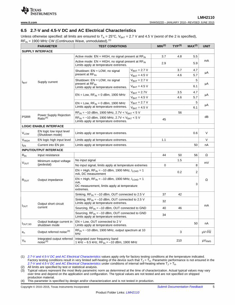
6.5 2.7-V and 4.5-V DC and AC Electrical CharacteristicsUnless otherwise specified: all limits are ensured to TA = 25°C, VBAT = 2.7 V and 4.5 V (worst of the 2 is specified),RFIN = 1900 MHz CW (Continuous Wave, unmodulated). (1)
PARAMETER TEST CONDITIONS MIN (2) TYP (3) MAX (2) UNITSUPPLY INTERFACE
Active mode: EN = HIGH, no signal present at RFIN 3.7 4.8 5.5mAActive mode: EN = HIGH, no signal present at RFIN 2.9 5.9Limits apply at temperature extremes.
VBAT = 2.7 V 3.7 4.7Shutdown: EN = LOW, no signal μApresent at RFIN. VBAT = 4.5 V 4.6 5.7Shutdown: EN = LOW, no signal VBAT = 2.7 V 5IBAT Supply current present at RFIN. μA
VBAT = 4.5 V 6.1Limits apply at temperature extremes.VBAT = 2.7V 3.5 4.7
EN = Low, RFIN = 0 dBm, 1900 MHz μAVBAT = 4.5 V 4.6 5.7VBAT = 2.7 V 5EN = Low, RFIN = 0 dBm, 1900 MHz μALimits apply at temperature extremes. VBAT = 4.5 V 6.1
RFIN = −10 dBm, 1900 MHz, 2.7V < VBAT < 5 V 56Power Supply RejectionPSRR dBRFIN = −10 dBm, 1900 MHz, 2.7V < VBAT < 5 VRatio (4) 45Limits apply at temperature extremes.
LOGIC ENABLE INTERFACEEN logic low input levelVLOW Limits apply at temperature extremes. 0.6 V(Shutdown mode)
VHIGH EN logic high input level Limits apply at temperature extremes. 1.1 VIEN Current into EN pin Limits apply at temperature extremes. 50 nAINPUT/OUTPUT INTERFACERIN Input resistance 44 50 56 Ω
No input signal 1.5Minimum output voltageVOUT mV(pedestal) No input signal, limits apply at temperature extremes 0 8EN = High, RFIN = –10 dBm, 1900 MHz, ILOAD = 1 0.2 2mA, DC measurementEN = High, RFIN = –10 dBm, 1900 MHz, ILOAD = 1ROUT Output impedance ΩmA, 3DC measurement, limits apply at temperatureextremes.Sinking, RFIN = –10 dBm, OUT connected to 2.5 V 37 42Sinking, RFIN = –10 dBm, OUT connected to 2.5 V 32Limits apply at temperature extremes.Output short circuitIOUT mAcurrent Sourcing, RFIN = –10 dBm, OUT connected to GND 40 46Sourcing, RFIN = –10 dBm, OUT connected to GND 34Limits apply at temperature extremes.
Output leakage current in EN = Low, OUT connected to 2 VIOUT,SD 50 nAshutdown mode Limits apply at temperature extremes.RFIN = −10 dBm, 1900 MHz, output spectrum at 10en Output referred noise (4) 3 µV√HzkHz
Integrated output referred Integrated over frequency bandVN 210 µVRMSnoise (4) 1 kHz – 6.5 kHz, RFIN = –10 dBm, 1900 MHz
(1) 2.7-V and 4.5-V DC and AC Electrical Characteristics values apply only for factory testing conditions at the temperature indicated.Factory testing conditions result in very limited self-heating of the device such that TJ = TA. Parametric performance is not ensured in the2.7-V and 4.5-V DC and AC Electrical Characteristics under conditions of internal self-heating where TJ > TA.
(2) All limits are specified by test or statistical analysis.(3) Typical values represent the most likely parametric norm as determined at the time of characterization. Actual typical values may vary
over time and depend on the application and configuration. The typical values are not tested and are not specified on shippedproduction material.
(4) This parameter is specified by design and/or characterization and is not tested in production.
Copyright © 2010–2015, Texas Instruments Incorporated Submit Documentation Feedback 5
Product Folder Links: LMH2110
LMH2110SNWS022D –JANUARY 2010–REVISED JUNE 2015 www.ti.com
2.7-V and 4.5-V DC and AC Electrical Characteristics (continued)Unless otherwise specified: all limits are ensured to TA = 25°C, VBAT = 2.7 V and 4.5 V (worst of the 2 is specified),
RFIN = 1900 MHz CW (Continuous Wave, unmodulated).(1)
PARAMETER TEST CONDITIONS MIN (2) TYP (3) MAX (2) UNITRF DETECTOR TRANSFERRFIN = 50 MHz (fit range –20 dBm to –10 dBm) (5)
Minimum power level,PMIN bottom end of dynamic Log conformance error within ±1 dB –39 dBm
rangeMaximum power level,PMAX Log conformance error within ±1 dB 7 dBmtop end of dynamic range
VMIN Minimum output voltage At PMIN 3 mVVMAX Maximum output voltage At PMAX 1.96 VKSLOPE Logarithmic slope 42.2 44.3 46.4 mV/dBPINT Logarithmic Intercept –38.6 –38.3 –38.0 dBm
±1-dB Log conformance error (ELC) 46±1-dB Log conformance error (ELC) 45Limits apply at temperature extremes.±3-dB Log Conformance Error (ELC) 51Dynamic Range forDR dB±3-dB Log conformance error (ELC)specified accuracy 50Limits apply at temperature extremes.±0.5-dB input referred variation over temperature(EVOT), from PMIN 42Limits apply at temperature extremes.
RF DETECTOR TRANSFERRFIN = 900 MHz (fit range –20 dBm to –10 dBm) (5)
Minimum power level,PMIN bottom end of dynamic Log conformance error within ±1 dB –38 dBm
rangeMaximum power level,PMAX Log conformance error within ±1 dB 0 dBmtop end of dynamic range
VMIN Minimum output voltage At PMIN 3 mVVMAX Maximum output voltage At PMAX 1.58 VKSLOPE Logarithmic slope 41.8 43.9 46 mV/dBPINT Logarithmic intercept –37.4 –37 –36.7 dBm
±1-dB Log conformance error (ELC) 38±1-dB Log conformance error (ELC) 37Limits apply at temperature extremes.±3-dB Log conformance error (ELC) 45±3-dB Log conformance error (ELC) 44Limits apply at temperature extremes.
Dynamic range for ±0.5-dB Input referred variation over temperatureDR dBspecified accuracy (EVOT), from PMIN 44Limits apply at temperature extremes.±0.3-dB Error for a 1dB Step (E1dB STEP) 41±0.3-dB Error for a 1dB Step (E1dB STEP) 38Limits apply at temperature extremes.±1-dB Error for a 10dB Step (E10dB 30 STEP) 32Limits apply at temperature extremes.
Input-referred variation W-CDMA Release 6/7/8,EMOD 0.08due to modulation –38 dBm < RFIN < –5 dBm dBLTE, –38 dBm < RFIN < –5 dBm 0.19
(5) All limits are specified by design and measurements which are performed on a limited number of samples. Limits represent the mean±3–sigma values. The typical value represents the statistical mean value.
6 Submit Documentation Feedback Copyright © 2010–2015, Texas Instruments Incorporated
Product Folder Links: LMH2110
LMH2110www.ti.com SNWS022D –JANUARY 2010–REVISED JUNE 2015
2.7-V and 4.5-V DC and AC Electrical Characteristics (continued)Unless otherwise specified: all limits are ensured to TA = 25°C, VBAT = 2.7 V and 4.5 V (worst of the 2 is specified),
RFIN = 1900 MHz CW (Continuous Wave, unmodulated).(1)
PARAMETER TEST CONDITIONS MIN (2) TYP (3) MAX (2) UNITRF DETECTOR TRANSFERRFIN = 1900 MHz (fit range –20 dBm to –10 dBm) (5)
Minimum power level,PMIN bottom end of dynamic Log conformance error within ±1 dB –36 dBm
rangeMaximum power level,PMAX Log conformance error within ±1 dB 0 dBmtop end of dynamic range
VMIN Minimum output voltage At PMIN 3 mVVMAX maximum output voltage At PMAX 1.5 VKSLOPE Logarithmic slope 41.8 43.9 46.1 mV/dBPINT Logarithmic Intercept –35.5 –35.1 –34.7 dBm
±1-dB Log conformance error (ELC) 36Limits apply at temperature extremes.±3-dB Log conformance Error (ELC) 45±3-dB Log conformance error (ELC) 43Limits apply at temperature extremes.±0.5-dB Input referred variation over temperatureDynamic range forDR (EVOT), from PMIN 41 dBspecified accuracy Limits apply at temperature extremes.±0.3-dB error for a 1-dB Step (E1dB STEP) 40±0.3-dB error for a 1-dB Step (E1dB STEP) 38Limits apply at temperature extremes.±1-dB error for a 10-dB Step (E10-dB 30 STEP) 30Limits apply at temperature extremes.W-CDMA Release 6/7/8, 0.09Input-referred variation –38 dBm < RFIN < –5 dBmEMOD dBdue to modulationLTE, –38 dBm < RFIN < –5 dBm 0.18
RFIN = 3500 MHz, fit range –15 dBm to –5 dBm (5)
Minimum power level,PMIN bottom end of dynamic Log conformance error within ±1 dB –31 dBm
rangeMaximum power level,PMAX Log conformance error within ±1 dB 6 dBmtop end of dynamic range
VMIN Minimum output voltage At PMIN 2 mVVMAX Maximum output voltage At PMAX 1.52 VKSLOPE Logarithmic slope 41.8 44 46.1 mV/dBPINT Logarithmic Intercept –30.5 –29.7 –28.8 dBm
±1-dB Log conformance error (ELC) 37±1-dB Log conformance error (ELC) 36Limits apply at temperature extremes.±3-dB Log conformance error (ELC) 44Dynamic range forDR dB±3-dB Log conformance error (ELC)specified accuracy 42Limits apply at temperature extremes.±0.5-dB Input referred variation over temperature(EVOT), from PMIN 39Limits apply at temperature extremes.
Copyright © 2010–2015, Texas Instruments Incorporated Submit Documentation Feedback 7
Product Folder Links: LMH2110
LMH2110SNWS022D –JANUARY 2010–REVISED JUNE 2015 www.ti.com
2.7-V and 4.5-V DC and AC Electrical Characteristics (continued)Unless otherwise specified: all limits are ensured to TA = 25°C, VBAT = 2.7 V and 4.5 V (worst of the 2 is specified),
RFIN = 1900 MHz CW (Continuous Wave, unmodulated).(1)
PARAMETER TEST CONDITIONS MIN (2) TYP (3) MAX (2) UNITRFIN = 5800 MHz, fit range –20 dBm to 3 dBm (5)
Minimum power level,PMIN bottom end of dynamic Log conformance error within ±1 dB –22 dBm
rangeMaximum power level,PMAX Log conformance error within ±1 dB 10 dBmtop end of dynamic range
VMIN Minimum output voltage At PMIN 3 mVVMAX Maximum output voltage At PMAX 1.34 VKSLOPE Logarithmic slope 42.5 44.8 47.1 mV/dBPINT Logarithmic Intercept –22 –21 –19.9 dBm
±1-dB Log conformance error (ELC) 32±1-dB Log conformance error (ELC) 31Limits apply at temperature extremes.±3-dB Log conformance error (ELC) 39Dynamic range forDR dB±3-dB Log conformance error (ELC)specified accuracy 37Limits apply at temperature extremes.±0.5-dB Input referred variation over temperature(EVOT), from PMIN 33Limits apply at temperature extremes.
6.6 Timing RequirementsMIN NOM MAX UNIT
Turnon time from shutdowntON 15 19 µsRFIN = –10 dBm, 1900 MHz, EN LOW-HIGH transition to OUT at 90%Rise time (1)
tR 2.2 µsSignal at RFIN from –20 dBm to 0 dBm, 10% to 90%, 1900 MHzFall time (1)
tF 31 µsSignal at RFIN from 0 dBm to –20 dBm, 90% to 10%, 1900 MHz
(1) This parameter is specified by design and/or characterization and is not tested in production.
8 Submit Documentation Feedback Copyright © 2010–2015, Texas Instruments Incorporated
Product Folder Links: LMH2110
RF INPUT POWER (dBm)
SIN
KIN
GO
UT
PU
TC
UR
RE
NT
(mA
)
60
50
40
30
20
10
0-40 -30 -20 -10 0 10
85°C
25°C-40°C
RFin = 1900 MHzOUT = 2.5V
RF INPUT POWER (dBm)
SO
UR
CIN
GO
UT
PU
TC
UR
RE
NT
(mA
)
60
50
40
30
20
10
0-40 -30 -20 -10 0 10
85°C
25°C-40°C
RFin = 1900 MHzOUT = 0V
0.5 0.6 0.7 0.8 0.9 1.0 1.1 1.2
7
6
5
4
3
2
1
0
ENABLE VOLTAGE (V)
SU
PP
LY C
UR
RE
NT
(m
A)
-40°C
85°C
25°C
RF INPUT POWER (dBm)
SU
PP
LY C
UR
RE
NT
(m
A)
8
7
6
5
4
3
2
1
0-40 -30 -20 -10 0 10
85°C25°C-40°C
0 1 2 3 4 5 6
8
7
6
5
4
3
2
1
0
SUPPLY VOLTAGE (V)
SU
PP
LY C
UR
RE
NT
(éA)
-40°C
85°C
25°C
EN = LOW
0 1 2 3 4 5 6
7
6
5
4
3
2
1
0
SUPPLY VOLTAGE (V)
SU
PP
LY C
UR
RE
NT
(m
A)
-40°C 85°C25°C
EN = HIGH
LMH2110www.ti.com SNWS022D –JANUARY 2010–REVISED JUNE 2015
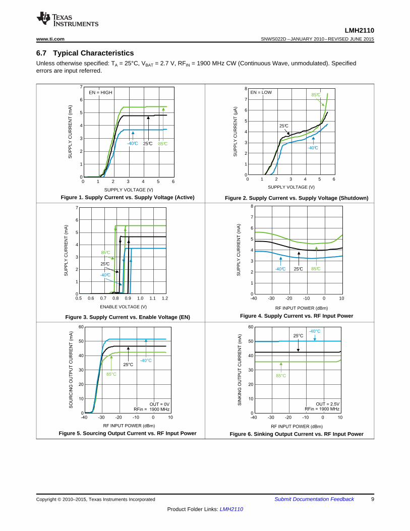
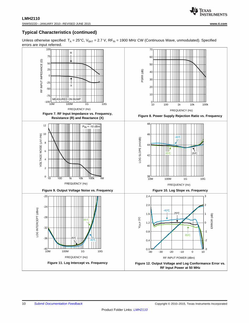
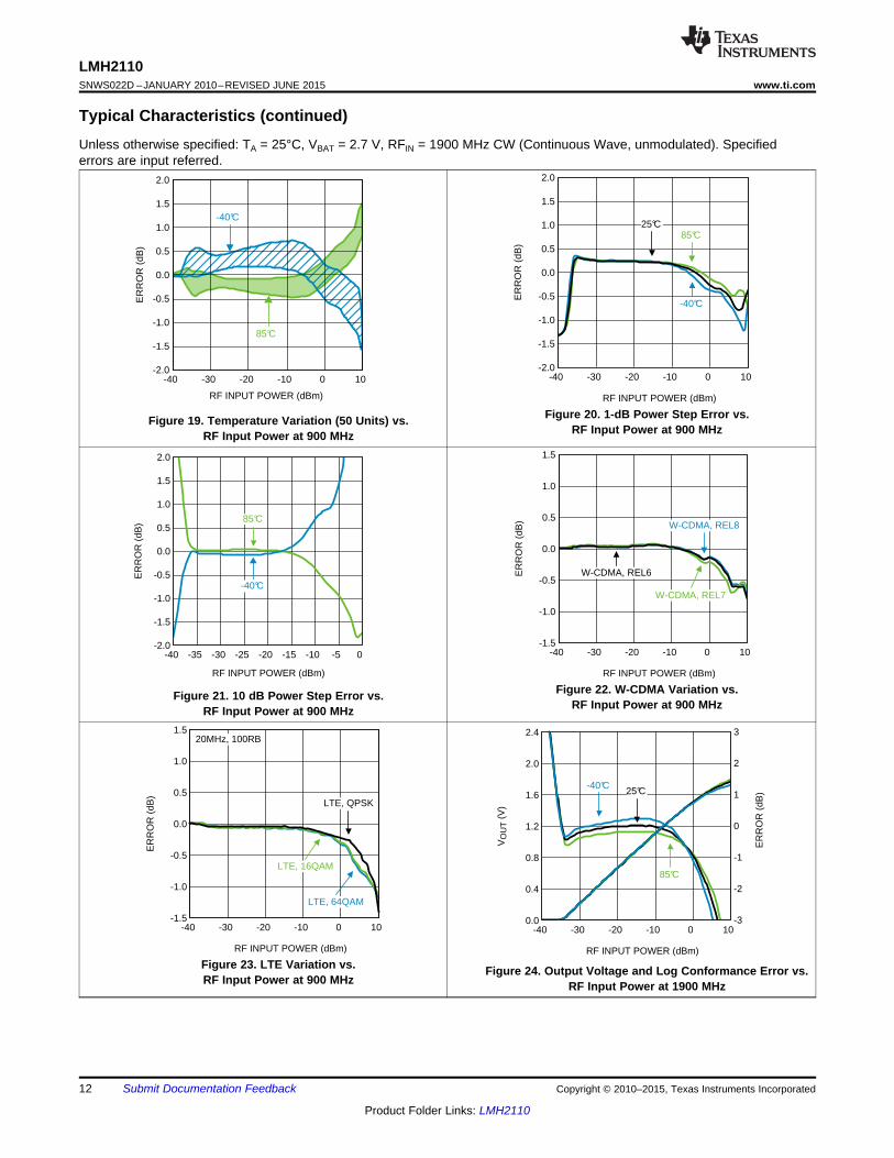
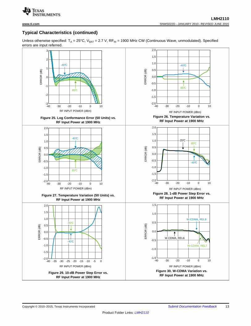
6.7 Typical CharacteristicsUnless otherwise specified: TA = 25°C, VBAT = 2.7 V, RFIN = 1900 MHz CW (Continuous Wave, unmodulated). Specifiederrors are input referred.
Figure 1. Supply Current vs. Supply Voltage (Active) Figure 2. Supply Current vs. Supply Voltage (Shutdown)
Figure 4. Supply Current vs. RF Input PowerFigure 3. Supply Current vs. Enable Voltage (EN)
Figure 5. Sourcing Output Current vs. RF Input Power Figure 6. Sinking Output Current vs. RF Input Power
Copyright © 2010–2015, Texas Instruments Incorporated Submit Documentation Feedback 9
Product Folder Links: LMH2110
-40 -30 -20 -10 0 10
2.4
2.0
1.6
1.2
0.8
0.4
0.0
85°C
ER
RO
R (
dB)
RF INPUT POWER (dBm)
VO
UT (
V)
-40°C
3
2
1
0
-1
-2
-3
25°C
FREQUENCY (Hz)
LOG
INT
ER
CE
PT
(dB
m)
-20
-24
-28
-32
-36
-4010M 100M 1G 10G
85°C
25°C-40°C
FREQUENCY (Hz)
LOG
SLO
PE
(m
V/d
B)
48
46
44
42
40
3810M 100M 1G 10G
85°C 25°C
-40°C
FREQUENCY (Hz)
PS
RR
(dB
)
70
60
50
40
30
20
10
010 100 1k 10k 100k
FREQUENCY (Hz)
RF
INP
UT
IMP
ED
AN
CE
(Ö) 100
755025
0-25-50-75
-100
10M 100M 1G 10G
R
X
MEASURED ON BUMP
100
75
50
25
0
-25
-50
-75
-100
LMH2110SNWS022D –JANUARY 2010–REVISED JUNE 2015 www.ti.com
Typical Characteristics (continued)Unless otherwise specified: TA = 25°C, VBAT = 2.7 V, RFIN = 1900 MHz CW (Continuous Wave, unmodulated). Specifiederrors are input referred.
Figure 7. RF Input Impedance vs. Frequency, Figure 8. Power Supply Rejection Ratio vs. FrequencyResistance (R) and Reactance (X)
Figure 9. Output Voltage Noise vs. Frequency Figure 10. Log Slope vs. Frequency
Figure 11. Log Intercept vs. Frequency Figure 12. Output Voltage and Log Conformance Error vs.RF Input Power at 50 MHz
10 Submit Documentation Feedback Copyright © 2010–2015, Texas Instruments Incorporated
Product Folder Links: LMH2110
RF INPUT POWER (dBm)
ER
RO
R (
dB)
85°C
-40 -30 -20 -10 0 10
3
2
1
0
-1
-2
-3
-40°C
-40 -30 -20 -10 0 10
2.0
1.5
1.0
0.5
0.0
-0.5
-1.0
-1.5
-2.0
RF INPUT POWER (dBm)
ER
RO
R (
dB)
-40°C
85°C
-40 -30 -20 -10 0 10
2.4
2.0
1.6
1.2
0.8
0.4
0.0
85°C
ER
RO
R (
dB)
RF INPUT POWER (dBm)
VO
UT (
V)
-40°C
3
2
1
0
-1
-2
-3
25°C
RF INPUT POWER (dBm)
ER
RO
R (
dB)
85°C
-40°C
-40 -30 -20 -10 0 10
2.0
1.5
1.0
0.5
0.0
-0.5
-1.0
-1.5
-2.0
RF INPUT POWER (dBm)
ER
RO
R (
dB)
85°C
-40°C
-40 -30 -20 -10 0 10
3
2
1
0
-1
-2
-3-40 -30 -20 -10 0 10
2.0
1.5
1.0
0.5
0.0
-0.5
-1.0
-1.5
-2.0
RF INPUT POWER (dBm)
ER
RO
R (
dB)
-40°C
85°C
LMH2110www.ti.com SNWS022D –JANUARY 2010–REVISED JUNE 2015
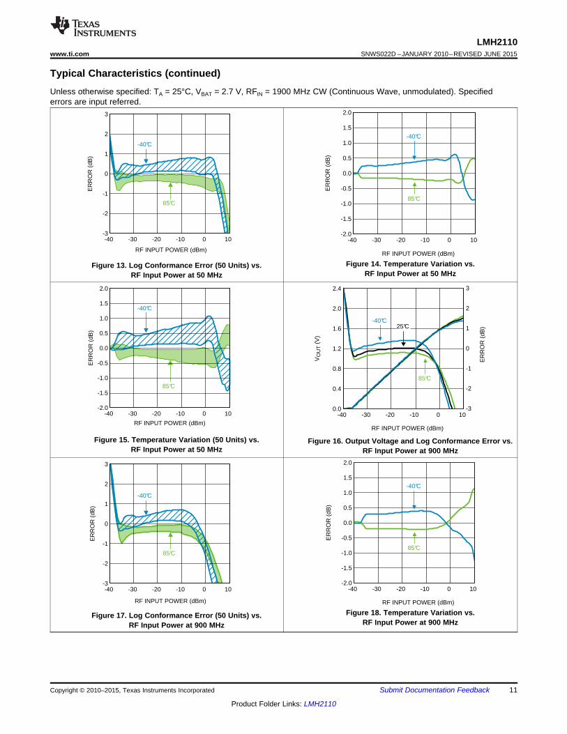
Typical Characteristics (continued)Unless otherwise specified: TA = 25°C, VBAT = 2.7 V, RFIN = 1900 MHz CW (Continuous Wave, unmodulated). Specifiederrors are input referred.
Figure 14. Temperature Variation vs.Figure 13. Log Conformance Error (50 Units) vs.RF Input Power at 50 MHzRF Input Power at 50 MHz
Figure 15. Temperature Variation (50 Units) vs. Figure 16. Output Voltage and Log Conformance Error vs.RF Input Power at 50 MHz RF Input Power at 900 MHz
Figure 18. Temperature Variation vs.Figure 17. Log Conformance Error (50 Units) vs.RF Input Power at 900 MHzRF Input Power at 900 MHz
Copyright © 2010–2015, Texas Instruments Incorporated Submit Documentation Feedback 11
Product Folder Links: LMH2110
2.4
2.0
1.6
1.2
0.8
0.4
0.0-40 -30 -20 -10 0 10
85°C
-40°C25°C
ER
RO
R (
dB)
RF INPUT POWER (dBm)
VO
UT (
V)
3
2
1
0
-1
-2
-3
RF INPUT POWER (dBm)
ER
RO
R (
dB)
1.5
1.0
0.5
0.0
-0.5
-1.0
-1.5-40 -30 -20 -10 0 10
LTE, 64QAM
LTE, 16QAM
LTE, QPSK
20MHz, 100RB
-40 -35 -30 -25 -20 -15 -10 -5 0
2.0
1.5
1.0
0.5
0.0
-0.5
-1.0
-1.5
-2.0
RF INPUT POWER (dBm)
ER
RO
R (
dB)
-40°C
85°C
RF INPUT POWER (dBm)
ER
RO
R (
dB)
1.5
1.0
0.5
0.0
-0.5
-1.0
-1.5-40 -30 -20 -10 0 10
W-CDMA, REL8
W-CDMA, REL7
W-CDMA, REL6
RF INPUT POWER (dBm)
ER
RO
R (
dB)
-40 -30 -20 -10 0 10
2.0
1.5
1.0
0.5
0.0
-0.5
-1.0
-1.5
-2.0
-40°C
85°C
-40 -30 -20 -10 0 10
2.0
1.5
1.0
0.5
0.0
-0.5
-1.0
-1.5
-2.0
RF INPUT POWER (dBm)
ER
RO
R (
dB)
-40°C
85°C25°C
LMH2110SNWS022D –JANUARY 2010–REVISED JUNE 2015 www.ti.com
Typical Characteristics (continued)Unless otherwise specified: TA = 25°C, VBAT = 2.7 V, RFIN = 1900 MHz CW (Continuous Wave, unmodulated). Specifiederrors are input referred.
Figure 20. 1-dB Power Step Error vs.Figure 19. Temperature Variation (50 Units) vs.RF Input Power at 900 MHzRF Input Power at 900 MHz
Figure 22. W-CDMA Variation vs.Figure 21. 10 dB Power Step Error vs.RF Input Power at 900 MHzRF Input Power at 900 MHz
Figure 23. LTE Variation vs. Figure 24. Output Voltage and Log Conformance Error vs.RF Input Power at 900 MHz RF Input Power at 1900 MHz
12 Submit Documentation Feedback Copyright © 2010–2015, Texas Instruments Incorporated
Product Folder Links: LMH2110
-40 -35 -30 -25 -20 -15 -10 -5 0
2.0
1.5
1.0
0.5
0.0
-0.5
-1.0
-1.5
-2.0
RF INPUT POWER (dBm)
ER
RO
R (
dB)
-40°C
85°C
RF INPUT POWER (dBm)
ER
RO
R (
dB)
1.5
1.0
0.5
0.0
-0.5
-1.0
-1.5-40 -30 -20 -10 0 10
W-CDMA, REL8
W-CDMA, REL7
W-CDMA, REL6
RF INPUT POWER (dBm)
ER
RO
R (
dB)
-40 -30 -20 -10 0 10
2.0
1.5
1.0
0.5
0.0
-0.5
-1.0
-1.5
-2.0
-40°C
85°C
-40 -30 -20 -10 0 10
2.0
1.5
1.0
0.5
0.0
-0.5
-1.0
-1.5
-2.0
RF INPUT POWER (dBm)
ER
RO
R (
dB)
-40°C
85°C25°C
RF INPUT POWER (dBm)
ER
RO
R (
dB)
85°C
-40 -30 -20 -10 0 10
3
2
1
0
-1
-2
-3
-40°C
-40 -30 -20 -10 0 10
2.0
1.5
1.0
0.5
0.0
-0.5
-1.0
-1.5
-2.0
RF INPUT POWER (dBm)
ER
RO
R (
dB)
-40°C
85°C
LMH2110www.ti.com SNWS022D –JANUARY 2010–REVISED JUNE 2015
Typical Characteristics (continued)Unless otherwise specified: TA = 25°C, VBAT = 2.7 V, RFIN = 1900 MHz CW (Continuous Wave, unmodulated). Specifiederrors are input referred.
Figure 26. Temperature Variation vs.Figure 25. Log Conformance Error (50 Units) vs.RF Input Power at 1900 MHzRF Input Power at 1900 MHz
Figure 28. 1-dB Power Step Error vs.Figure 27. Temperature Variation (50 Units) vs.RF Input Power at 1900 MHzRF Input Power at 1900 MHz
Figure 30. W-CDMA Variation vs.Figure 29. 10-dB Power Step Error vs.RF Input Power at 1900 MHzRF Input Power at 1900 MHz
Copyright © 2010–2015, Texas Instruments Incorporated Submit Documentation Feedback 13
Product Folder Links: LMH2110
RF INPUT POWER (dBm)
ER
RO
R (
dB)
-40 -30 -20 -10 0 10
2.0
1.5
1.0
0.5
0.0
-0.5
-1.0
-1.5
-2.0
-40°C
85°C
2.4
2.0
1.6
1.2
0.8
0.4
0.0-40 -30 -20 -10 0 10
85°C
-40°C 25°C
ER
RO
R (
dB)
RF INPUT POWER (dBm)
VO
UT (
V)
3
2
1
0
-1
-2
-3
RF INPUT POWER (dBm)
ER
RO
R (
dB)
85°C
-40 -30 -20 -10 0 10
3
2
1
0
-1
-2
-3
-40°C
-40 -30 -20 -10 0 10
2.0
1.5
1.0
0.5
0.0
-0.5
-1.0
-1.5
-2.0
RF INPUT POWER (dBm)
ER
RO
R (
dB)-40°C
85°C
2.4
2.0
1.6
1.2
0.8
0.4
0.0-40 -30 -20 -10 0 10
85°C
-40°C25°C
ER
RO
R (
dB)
RF INPUT POWER (dBm)
VO
UT (
V)
3
2
1
0
-1
-2
-3
RF INPUT POWER (dBm)
ER
RO
R (
dB)
1.5
1.0
0.5
0.0
-0.5
-1.0
-1.5-40 -30 -20 -10 0 10
LTE, 64QAM
LTE, 16QAM
LTE, QPSK
20MHz, 100RB
LMH2110SNWS022D –JANUARY 2010–REVISED JUNE 2015 www.ti.com
Typical Characteristics (continued)Unless otherwise specified: TA = 25°C, VBAT = 2.7 V, RFIN = 1900 MHz CW (Continuous Wave, unmodulated). Specifiederrors are input referred.
Figure 31. LTE Input referred Variation vs. Figure 32. Output Voltage and Log Conformance Error vs.RF Input Power at 1900 MHz RF Input Power at 3500 MHz
Figure 34. Temperature Variation vs.Figure 33. Log Conformance Error (50 Units) vs.RF Input Power at 3500 MHzRF Input Power at 3500 MHz
Figure 35. Temperature Variation (50 Units) vs. Figure 36. Output Voltage and Log Conformance Error vs.RF Input Power at 3500 MHz RF Input Power at 5800 MHz
14 Submit Documentation Feedback Copyright © 2010–2015, Texas Instruments Incorporated
Product Folder Links: LMH2110
-40 -30 -20 -10 0 10
2.0
1.5
1.0
0.5
0.0
-0.5
-1.0
-1.5
-2.0
RF INPUT POWER (dBm)
ER
RO
R (
dB)
-40°C
85°C
RF INPUT POWER (dBm)
ER
RO
R (
dB)
-40 -30 -20 -10 0 10
-40°C
85°C
2.0
1.5
1.0
0.5
0.0
-0.5
-1.0
-1.5
-2.0
2.4
2.0
1.6
1.2
0.8
0.4
0.0-40 -30 -20 -10 0 10
85°C
-40°C 25°C
ER
RO
R (
dB)
RF INPUT POWER (dBm)
VO
UT (
V)
3
2
1
0
-1
-2
-3
RF INPUT POWER (dBm)
ER
RO
R (
dB)
85°C
-40 -30 -20 -10 0 10
3
2
1
0
-1
-2
-3
-40°C
-40 -30 -20 -10 0 10
2.0
1.5
1.0
0.5
0.0
-0.5
-1.0
-1.5
-2.0
RF INPUT POWER (dBm)
ER
RO
R (
dB)
-40°C
85°C
LMH2110www.ti.com SNWS022D –JANUARY 2010–REVISED JUNE 2015
Typical Characteristics (continued)Unless otherwise specified: TA = 25°C, VBAT = 2.7 V, RFIN = 1900 MHz CW (Continuous Wave, unmodulated). Specifiederrors are input referred.
Figure 38. Temperature Variation vs.Figure 37. Log Conformance Error (50 Units) vs.RF Input Power at 5800 MHzRF Input Power at 5800 MHz
Figure 39. Temperature Variation (50 Units) vs. Figure 40. Output Voltage and Log Conformance Error vs.RF Input Power at 5800 MHz RF Input Power at 8000 MHz
Figure 41. Temperature Variation vs.RF Input Power at 8000 MHz
Copyright © 2010–2015, Texas Instruments Incorporated Submit Documentation Feedback 15
Product Folder Links: LMH2110
RFINB1 OUT A2
GND
VDD
B2,
C1
A1
V/I
V/I
A
LDO
C2 EN
Internal
Supply
EXP
EXP
LMH2110SNWS022D –JANUARY 2010–REVISED JUNE 2015 www.ti.com
7 Detailed Description
7.1 OverviewThe LMH2110 is a high-performance logarithmic root mean square (RMS) power detector which measures theactual power content of a signal. The device has a RF input power detection range from –40 dBm to 5 dBm andprovides accurate output voltage that relates linearly to the RF input power in dBm. This output voltage exhibitshigh temperature insensitivity ranging ±0.25 dB.
The device has an internal low dropout linear regulator (LDO) making the device insensitive to input supplyvariation and allowing operation from a wide input supply range from 2.7 V to 5 V. Additional features includemulti-band operation from 50 MHz to 8 GHz, shutdown functionality to save power, and minimal slope andintercept variation.
7.2 Functional Block Diagram
7.3 Feature Description
7.3.1 Accurate Power MeasurementDetectors have evolved over the years along with the communication standards. Newer communicationstandards like LTE and W-CDMA raise the need for more advanced accurate power detectors. To be able todistinguish the various detector types it is important to understand the ideal power measurement and how apower measurement is implemented.
Power is a metric for the average energy content of a signal. By definition it is not a function of the signal shapeover time. In other words, the power content of a 0-dBm sine wave is identical to the power content of a 0-dBmsquare wave or a 0-dBm W-CDMA signal; all these signals have the same average power content.
16 Submit Documentation Feedback Copyright © 2010–2015, Texas Instruments Incorporated
Product Folder Links: LMH2110
v(t)2dt³1T
VRMS =
P = dt =T1 T
0³v(t)2
R
VRMS2
R
LMH2110www.ti.com SNWS022D –JANUARY 2010–REVISED JUNE 2015
Feature Description (continued)The average power can be described by Equation 1:
where• T is the time interval over which is averaged• v(t) is the instantaneous voltage at time t• R is the resistance in which the power is dissipated• VRMS is the equivalent RMS voltage (1)
According to aforementioned formula for power, an exact power measurement can be done via measuring theRMS voltage (VRMS) of a signal. The RMS voltage is described by:
(2)
Implementing the exact formula for RMS can be challenging. A simplification can be made in determining theaverage power when information about the waveform is available. If the signal shape is known, the relationshipbetween RMS value and, for instance, the peak value of the RF signal is also known. It thus enables ameasurement based on measuring peak voltage rather than measuring the RMS voltage. To calculate the RMSvalue (and therewith the average power), the measured peak voltage is translated into an RMS voltage based onthe waveform characteristics. A few examples:• Sine wave: VRMS = VPEAK / √2• Square wave: VRMS = VPEAK• Saw-tooth wave: VRMS = VPEAK / √3
For more complex waveforms it is not always easy to determine the exact relationship between RMS value andpeak value. A peak measurement can then become impractical. An approximation can be used for the VRMS toVPEAK relationship but it can result in a less-accurate average power estimate.
Depending on the detection mechanism, power detectors may produce a slightly different output signal inresponse to more complex waveforms, even though the average power level of these signals are the same. Thiserror is due to the fact that not all power detectors strictly implement the definition for signal power, being theRMS of the signal. To cover for the systematic error in the output response of a detector, calibration can beused. After calibration a look-up table corrects for the error. Multiple look-up tables can be created for differentmodulation schemes.
7.3.2 Types of RF DetectorsThe following is an overview of detectors based on their detection principle. Detectors discussed in detail are:• Peak Detectors• LOG Amp Detectors• RMS Detectors
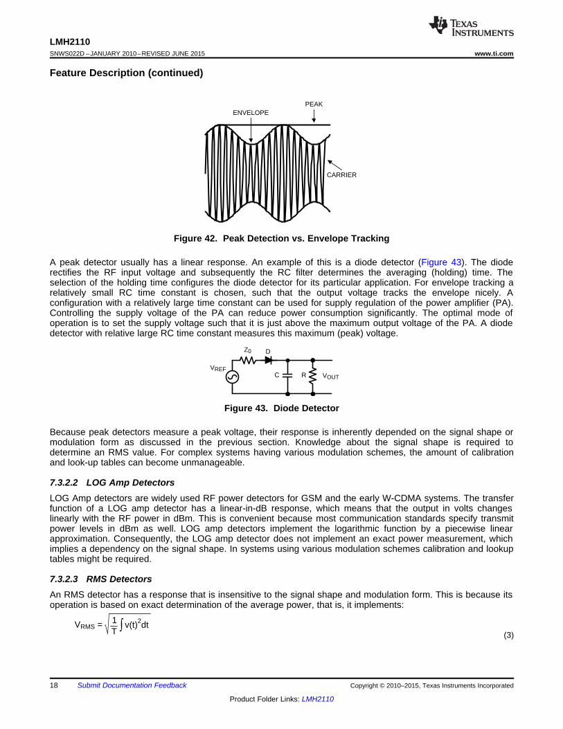
7.3.2.1 Peak DetectorsA peak detector is one of the simplest types of detectors. According to the naming, the peak detector stores thehighest value arising in a certain time window. However, usually a peak detector is used with a relative longholding time when compared to the carrier frequency and a relative short holding time with respect to theenvelope frequency. In this way a peak detector is used as AM demodulator or envelope tracker (Figure 42).
Copyright © 2010–2015, Texas Instruments Incorporated Submit Documentation Feedback 17
Product Folder Links: LMH2110
v(t)2dt³1T
VRMS =
C R VOUT
Z0 D
VREF
CARRIER
PEAKENVELOPE
LMH2110SNWS022D –JANUARY 2010–REVISED JUNE 2015 www.ti.com
Feature Description (continued)
Figure 42. Peak Detection vs. Envelope Tracking
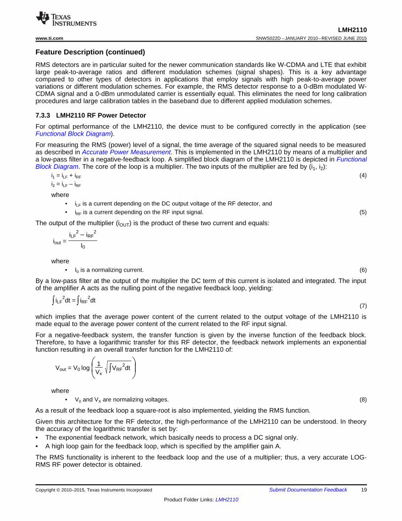
A peak detector usually has a linear response. An example of this is a diode detector (Figure 43). The dioderectifies the RF input voltage and subsequently the RC filter determines the averaging (holding) time. Theselection of the holding time configures the diode detector for its particular application. For envelope tracking arelatively small RC time constant is chosen, such that the output voltage tracks the envelope nicely. Aconfiguration with a relatively large time constant can be used for supply regulation of the power amplifier (PA).Controlling the supply voltage of the PA can reduce power consumption significantly. The optimal mode ofoperation is to set the supply voltage such that it is just above the maximum output voltage of the PA. A diodedetector with relative large RC time constant measures this maximum (peak) voltage.
Figure 43. Diode Detector
Because peak detectors measure a peak voltage, their response is inherently depended on the signal shape ormodulation form as discussed in the previous section. Knowledge about the signal shape is required todetermine an RMS value. For complex systems having various modulation schemes, the amount of calibrationand look-up tables can become unmanageable.
7.3.2.2 LOG Amp DetectorsLOG Amp detectors are widely used RF power detectors for GSM and the early W-CDMA systems. The transferfunction of a LOG amp detector has a linear-in-dB response, which means that the output in volts changeslinearly with the RF power in dBm. This is convenient because most communication standards specify transmitpower levels in dBm as well. LOG amp detectors implement the logarithmic function by a piecewise linearapproximation. Consequently, the LOG amp detector does not implement an exact power measurement, whichimplies a dependency on the signal shape. In systems using various modulation schemes calibration and lookuptables might be required.
7.3.2.3 RMS DetectorsAn RMS detector has a response that is insensitive to the signal shape and modulation form. This is because itsoperation is based on exact determination of the average power, that is, it implements:
(3)
18 Submit Documentation Feedback Copyright © 2010–2015, Texas Instruments Incorporated
Product Folder Links: LMH2110
VRF2dt³
1Vx
¸¹
ᬩ
§Vout = V0 log
iLF2dt =³ iRF
2dt³
iout =iLF
2 iRF2
I0
LMH2110www.ti.com SNWS022D –JANUARY 2010–REVISED JUNE 2015
Feature Description (continued)RMS detectors are in particular suited for the newer communication standards like W-CDMA and LTE that exhibitlarge peak-to-average ratios and different modulation schemes (signal shapes). This is a key advantagecompared to other types of detectors in applications that employ signals with high peak-to-average powervariations or different modulation schemes. For example, the RMS detector response to a 0-dBm modulated W-CDMA signal and a 0-dBm unmodulated carrier is essentially equal. This eliminates the need for long calibrationprocedures and large calibration tables in the baseband due to different applied modulation schemes.
7.3.3 LMH2110 RF Power DetectorFor optimal performance of the LMH2110, the device must to be configured correctly in the application (seeFunctional Block Diagram).
For measuring the RMS (power) level of a signal, the time average of the squared signal needs to be measuredas described in Accurate Power Measurement. This is implemented in the LMH2110 by means of a multiplier anda low-pass filter in a negative-feedback loop. A simplified block diagram of the LMH2110 is depicted in FunctionalBlock Diagram. The core of the loop is a multiplier. The two inputs of the multiplier are fed by (i1, i2):
i1 = iLF + iRF (4)i2 = iLF – iRF
where• iLF is a current depending on the DC output voltage of the RF detector, and• iRF is a current depending on the RF input signal. (5)
The output of the multiplier (iOUT) is the product of these two current and equals:
where• I0 is a normalizing current. (6)
By a low-pass filter at the output of the multiplier the DC term of this current is isolated and integrated. The inputof the amplifier A acts as the nulling point of the negative feedback loop, yielding:
(7)
which implies that the average power content of the current related to the output voltage of the LMH2110 ismade equal to the average power content of the current related to the RF input signal.
For a negative-feedback system, the transfer function is given by the inverse function of the feedback block.Therefore, to have a logarithmic transfer for this RF detector, the feedback network implements an exponentialfunction resulting in an overall transfer function for the LMH2110 of:
where• V0 and VX are normalizing voltages. (8)
As a result of the feedback loop a square-root is also implemented, yielding the RMS function.
Given this architecture for the RF detector, the high-performance of the LMH2110 can be understood. In theorythe accuracy of the logarithmic transfer is set by:• The exponential feedback network, which basically needs to process a DC signal only.• A high loop gain for the feedback loop, which is specified by the amplifier gain A.
The RMS functionality is inherent to the feedback loop and the use of a multiplier; thus, a very accurate LOG-RMS RF power detector is obtained.
Copyright © 2010–2015, Texas Instruments Incorporated Submit Documentation Feedback 19
Product Folder Links: LMH2110
LMH2110SNWS022D –JANUARY 2010–REVISED JUNE 2015 www.ti.com
Feature Description (continued)To ensure a low dependency on the supply voltage, the internal detector circuitry is supplied via a low drop-out(LDO) regulator. This enables the usage of a wide range of supply voltage (2.7 V to 5 V) in combination with alow sensitivity of the output signal for the external supply voltage.
7.3.3.1 RF InputRefer to Application With Resistive Divider for more details and applications.
7.3.3.2 EnableTo save power, the LMH2110 can be brought into a low-power shutdown mode by means of the enable pin (EN).The device is active for EN = HIGH (VEN>1.1 V) and in the low-power shutdown mode for EN = LOW(VEN < 0.6 V). In this state the output of the LMH2110 is switched to a high impedance mode. This highimpedance mode prevents the discharge of the optional low-pass filter which is good for the power efficiency.Using the shutdown function, care must be taken not to exceed the absolute maximum ratings. Because thedevice has an internal operating voltage of 2.5 V, the voltage level on the enable must not be higher than 3 V toprevent damage to the device. Also enable voltage levels lower than 400 mV below GND must be prevented. Inboth cases the ESD devices start to conduct when the enable voltage range is exceeded, and excessive currentis drawn. A correct operation is not ensured then. The absolute maximum ratings are also exceeded when theenable (EN) is switched to HIGH (from shutdown to active mode) while the supply voltage is switched off. Thissituation must be prevented at all times. A possible solution to protect the device is to add a resistor of 1 kΩ inseries with the enable input to limit the current.
7.3.3.3 OutputRefer to Application With Low-Pass Output Filter for Residual Ripple Reduction for more details and applications.
7.3.3.4 SupplyThe LMH2110 has an internal LDO to handle supply voltages between 2.7 V to 5 V. This enables a directconnection to the battery in cell-phone applications. The high PSRR of the LMH2110 ensures that theperformance is constant over its power supply range.
7.4 Device Functional ModesTo save power, the LMH2120 has an Enable/Disable feature that can bring the device in low-power shutdownmode. For implementation details, refer to Enable.
20 Submit Documentation Feedback Copyright © 2010–2015, Texas Instruments Incorporated
Product Folder Links: LMH2110
PAANTENNA
RF
50:
CS
RS
COUPLERVGA
BASEBAND
GAIN
ADC
EN
OPTIONAL
RFINOUT
VDD
GND
B1A1
A2
B2, C1
LMH2110
C2EN
LMH2110www.ti.com SNWS022D –JANUARY 2010–REVISED JUNE 2015
8 Application and Implementation
NOTEInformation in the following applications sections is not part of the TI componentspecification, and TI does not warrant its accuracy or completeness. TI’s customers areresponsible for determining suitability of components for their purposes. Customers mustvalidate and test their design implementation to confirm system functionality.
8.1 Application InformationThe LMH2110 is a 45-dB Logarithmic RMS power detector particularly suited for accurate power measurementsof modulated RF signals that exhibit large peak-to-average ratios (PARs). The RMS detector implements theexact definition of power resulting in a power measurement insensitive to high PARs. Such signals areencountered, for exampe, in LTE and W-CDMA applications. The LMH2110 has an RF frequency range from50 MHz to 8 GHz. It provides an output voltage that relates linearly to the RF input power in dBm. Its outputvoltage is highly insensitive to temperature and supply variations.
8.2 Typical Applications
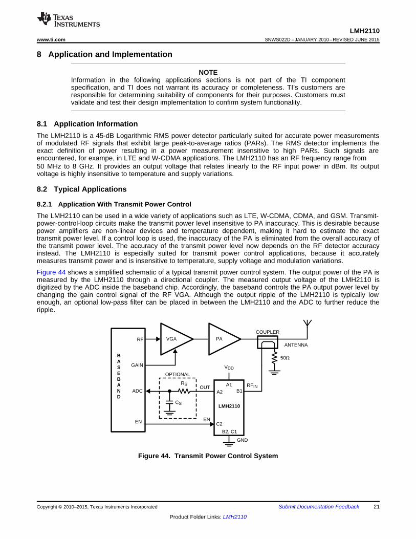
8.2.1 Application With Transmit Power ControlThe LMH2110 can be used in a wide variety of applications such as LTE, W-CDMA, CDMA, and GSM. Transmit-power-control-loop circuits make the transmit power level insensitive to PA inaccuracy. This is desirable becausepower amplifiers are non-linear devices and temperature dependent, making it hard to estimate the exacttransmit power level. If a control loop is used, the inaccuracy of the PA is eliminated from the overall accuracy ofthe transmit power level. The accuracy of the transmit power level now depends on the RF detector accuracyinstead. The LMH2110 is especially suited for transmit power control applications, because it accuratelymeasures transmit power and is insensitive to temperature, supply voltage and modulation variations.
Figure 44 shows a simplified schematic of a typical transmit power control system. The output power of the PA ismeasured by the LMH2110 through a directional coupler. The measured output voltage of the LMH2110 isdigitized by the ADC inside the baseband chip. Accordingly, the baseband controls the PA output power level bychanging the gain control signal of the RF VGA. Although the output ripple of the LMH2110 is typically lowenough, an optional low-pass filter can be placed in between the LMH2110 and the ADC to further reduce theripple.
Figure 44. Transmit Power Control System
Copyright © 2010–2015, Texas Instruments Incorporated Submit Documentation Feedback 21
Product Folder Links: LMH2110
LMH2110SNWS022D –JANUARY 2010–REVISED JUNE 2015 www.ti.com
Typical Applications (continued)8.2.1.1 Design RequirementsSome of the design requirements for this logarithmic RMS power detector include:
Table 1. Design ParametersDESIGN PARAMETER EXAMPLE VALUE
Supply voltage 2.7 VRF input frequency (unmodulated continuous wave) 1900 MHz
Minimum power level –36 dBmMaximum power level 0 dBm
Maximum output voltage 1.5 V
8.2.1.2 Detailed Design Procedure
8.2.1.2.1 Specifying Detector Performance
The performance of the LMH2110 can be expressed by a variety of parameters.
8.2.1.2.1.1 Dynamic Range
The LMH2110 is designed to have a predictable and accurate response over a certain input power range. This iscalled the dynamic range (DR) of a detector. For determining the dynamic range a couple of different criteria canbe used. The most commonly used ones are:• Log conformance error, ELC• Variation over temperature error, EVOT• 1-dB step error, E1 dB• 10-dB step error, E10 dB• Variation due to modulation, EMOD
The specified dynamic range is the range in which the specified error metric is within a predefined window. SeeLog Conformance Error, Variation Over Temperature Error, Variation Over Temperature Error, 1-dB Step Error,10-dB Step Error, and Variation Due to Modulation for an explanation of these errors.
8.2.1.2.1.2 Log Conformance Error
The LMH2110 implements a logarithmic function. In order to describe how close the transfer is to an ideallogarithmic function the log conformance error is used. To calculate the log conformance error the detectortransfer function is modeled as a linear-in-dB relationship between the input power and the output voltage.
22 Submit Documentation Feedback Copyright © 2010–2015, Texas Instruments Incorporated
Product Folder Links: LMH2110
ELC =VOUT KSLOPE 25qC (PIN PINT 25qC)
KSLOPE 25qC
RF INPUT POWER (dBm)
VO
UT
(V)
2.4
2.0
1.6
1.2
0.8
0.4
0.0-50 -30 -20 -10 0 10
PINT
Ideal LOG function
Detectorresponse
KSLOPE
LMH2110www.ti.com SNWS022D –JANUARY 2010–REVISED JUNE 2015
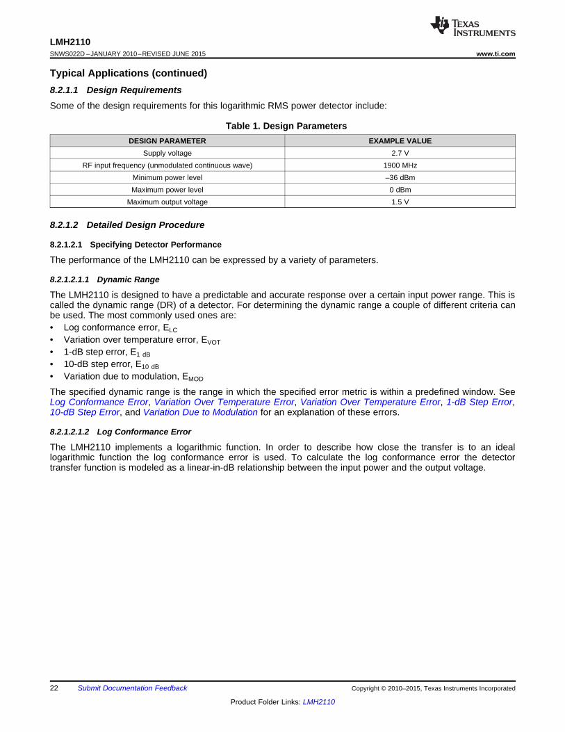
The ideal linear-in-dB transfer is modeled by 2 parameters:• Slope• Intercept
and is described by Equation 9:VOUT = KSLOPE (PIN – PINT)
where• KSLOPE is the slope of the line in mV/dB• PIN the input power level• PINT is the power level in dBm at which the line intercepts VOUT = 0 V (see Figure 45). (9)
Figure 45. Ideal Logarithmic Response
To determine the log conformance error two steps are required:1. Determine the best fitted line at 25°C.2. Determine the difference between the actual data and the best fitted line.
The best fit can be determined by standard routines. A careful selection of the fit range is important. The fit rangemust be within the normal range of operation of the device. Outcome of the fit is KSLOPE and PINT.
Subsequently, the difference between the actual data and the best fitted line is determined. The log conformanceis specified as an input referred error. The output referred error is therefore divided by the KSLOPE to obtain theinput referred error. The log conformance error is calculated by Equation 10:
where• VOUT is the measured output voltage at a power level at PIN at a temperature. KSLOPE 25°C (mV/dB).• PINT 25°C (dBm) are the parameters of the best fitted line of the 25°C transfer. (10)
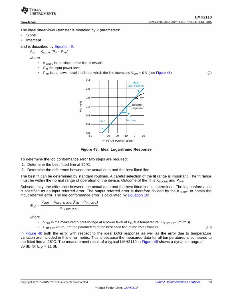
In Figure 46 both the error with respect to the ideal LOG response as well as the error due to temperaturevariation are included in this error metric. This is because the measured data for all temperatures is compared tothe fitted line at 25°C. The measurement result of a typical LMH2110 in Figure 46 shows a dynamic range of36 dB for ELC = ±1 dB.
Copyright © 2010–2015, Texas Instruments Incorporated Submit Documentation Feedback 23
Product Folder Links: LMH2110
-40 -30 -20 -10 0 10
2.0
1.5
1.0
0.5
0.0
-0.5
-1.0
-1.5
-2.0
RF INPUT POWER (dBm)
ER
RO
R (
dB)
-40°C
85°C
2.4
2.0
1.6
1.2
0.8
0.4
0.0-40 -30 -20 -10 0 10
85°C
-40°C25°C
ER
RO
R (
dB)
RF INPUT POWER (dBm)
VO
UT (
V)
3
2
1
0
-1
-2
-3
LMH2110SNWS022D –JANUARY 2010–REVISED JUNE 2015 www.ti.com
Figure 46. VOUT and ELC vs. RF input Power at 1900 MHz
8.2.1.2.1.3 Variation Over Temperature Error
In contrast to the log conformance error, the variation over temperature error (EVOT) purely measures the errordue to temperature variation. The measured output voltage at 25°C is subtracted from the output voltage atanother temperature. Subsequently, it is translated into an input referred error by dividing it by KSLOPE at 25°C.Variation over temperature is given by Equation 11:
EVOT = (VOUT_TEMP – VOUT 25°C) / KSLOPE 25°C (11)
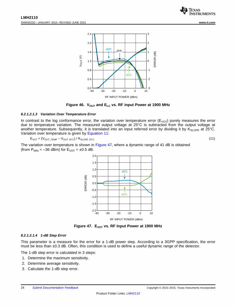
The variation over temperature is shown in Figure 47, where a dynamic range of 41 dB is obtained(from PMIN = –36 dBm) for EVOT = ±0.5 dB.
Figure 47. EVOT vs. RF Input Power at 1900 MHz
8.2.1.2.1.4 1-dB Step Error
This parameter is a measure for the error for a 1-dB power step. According to a 3GPP specification, the errormust be less than ±0.3 dB. Often, this condition is used to define a useful dynamic range of the detector.
The 1-dB step error is calculated in 3 steps:1. Determine the maximum sensitivity.2. Determine average sensitivity.3. Calculate the 1-dB step error.
24 Submit Documentation Feedback Copyright © 2010–2015, Texas Instruments Incorporated
Product Folder Links: LMH2110
P P+10 dB
PT PT+X
V2
V1
RFIN (dBm)
VO
UT (
V)
Temp (T)response
25°C response
-40 -30 -20 -10 0 10
2.0
1.5
1.0
0.5
0.0
-0.5
-1.0
-1.5
-2.0
RF INPUT POWER (dBm)
ER
RO
R (
dB)
-40°C
85°C25°C
LMH2110www.ti.com SNWS022D –JANUARY 2010–REVISED JUNE 2015
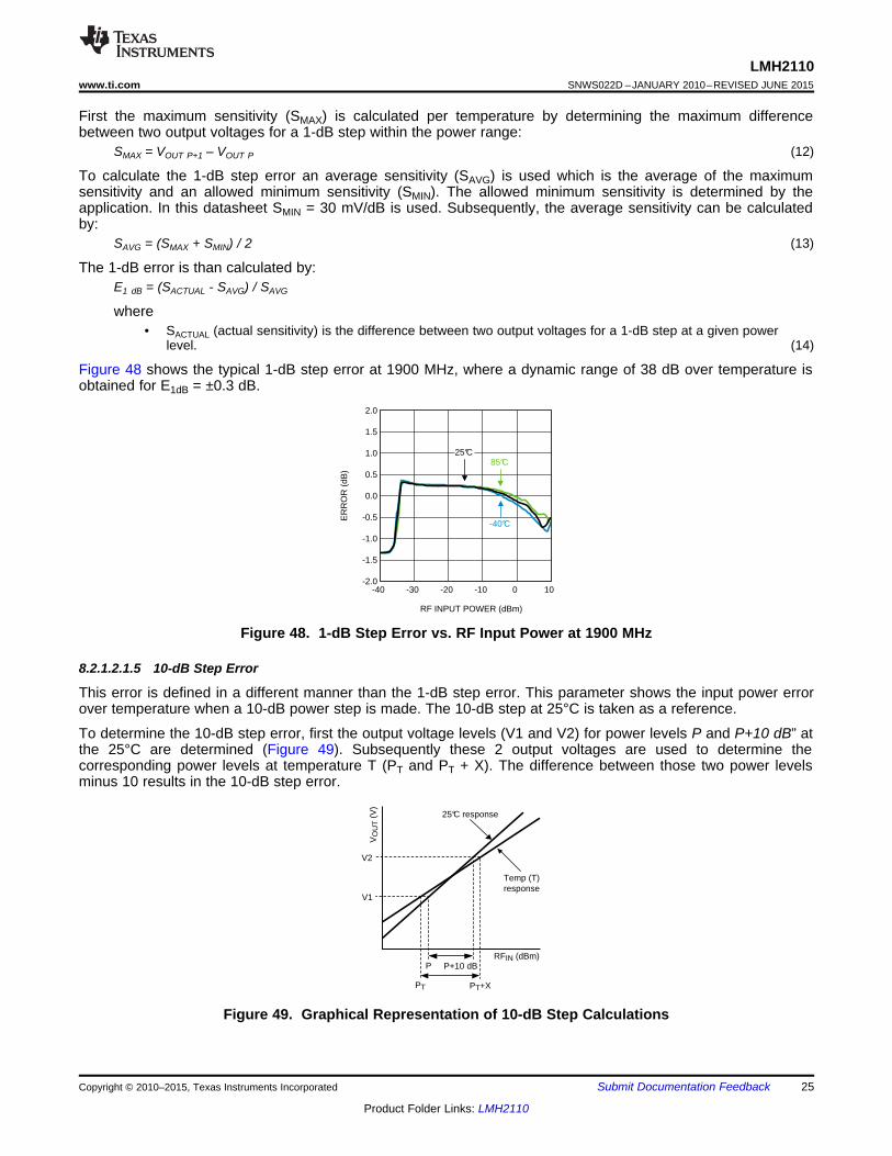
First the maximum sensitivity (SMAX) is calculated per temperature by determining the maximum differencebetween two output voltages for a 1-dB step within the power range:
SMAX = VOUT P+1 – VOUT P (12)
To calculate the 1-dB step error an average sensitivity (SAVG) is used which is the average of the maximumsensitivity and an allowed minimum sensitivity (SMIN). The allowed minimum sensitivity is determined by theapplication. In this datasheet SMIN = 30 mV/dB is used. Subsequently, the average sensitivity can be calculatedby:
SAVG = (SMAX + SMIN) / 2 (13)
The 1-dB error is than calculated by:E1 dB = (SACTUAL - SAVG) / SAVG
where• SACTUAL (actual sensitivity) is the difference between two output voltages for a 1-dB step at a given power
level. (14)
Figure 48 shows the typical 1-dB step error at 1900 MHz, where a dynamic range of 38 dB over temperature isobtained for E1dB = ±0.3 dB.
Figure 48. 1-dB Step Error vs. RF Input Power at 1900 MHz
8.2.1.2.1.5 10-dB Step Error
This error is defined in a different manner than the 1-dB step error. This parameter shows the input power errorover temperature when a 10-dB power step is made. The 10-dB step at 25°C is taken as a reference.
To determine the 10-dB step error, first the output voltage levels (V1 and V2) for power levels P and P+10 dB” atthe 25°C are determined (Figure 49). Subsequently these 2 output voltages are used to determine thecorresponding power levels at temperature T (PT and PT + X). The difference between those two power levelsminus 10 results in the 10-dB step error.
Figure 49. Graphical Representation of 10-dB Step Calculations
Copyright © 2010–2015, Texas Instruments Incorporated Submit Documentation Feedback 25
Product Folder Links: LMH2110
RF INPUT POWER (dBm)
ER
RO
R (
dB)
1.5
1.0
0.5
0.0
-0.5
-1.0
-1.5-40 -30 -20 -10 0 10
W-CDMA, REL8
W-CDMA, REL7
W-CDMA, REL6
-40 -35 -30 -25 -20 -15 -10 -5 0
2.0
1.5
1.0
0.5
0.0
-0.5
-1.0
-1.5
-2.0
RF INPUT POWER (dBm)
ER
RO
R (
dB)
-40°C
85°C
LMH2110SNWS022D –JANUARY 2010–REVISED JUNE 2015 www.ti.com
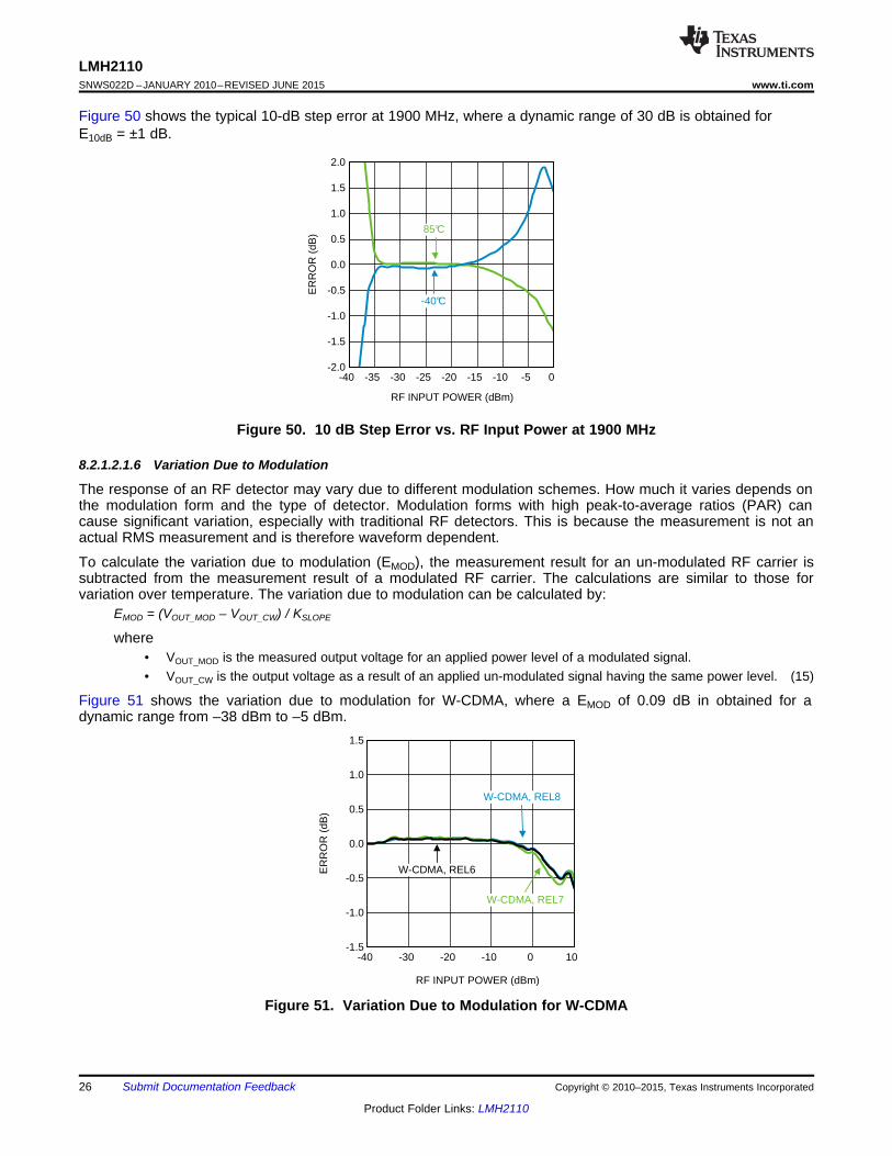
Figure 50 shows the typical 10-dB step error at 1900 MHz, where a dynamic range of 30 dB is obtained forE10dB = ±1 dB.
Figure 50. 10 dB Step Error vs. RF Input Power at 1900 MHz
8.2.1.2.1.6 Variation Due to Modulation
The response of an RF detector may vary due to different modulation schemes. How much it varies depends onthe modulation form and the type of detector. Modulation forms with high peak-to-average ratios (PAR) cancause significant variation, especially with traditional RF detectors. This is because the measurement is not anactual RMS measurement and is therefore waveform dependent.
To calculate the variation due to modulation (EMOD), the measurement result for an un-modulated RF carrier issubtracted from the measurement result of a modulated RF carrier. The calculations are similar to those forvariation over temperature. The variation due to modulation can be calculated by:
EMOD = (VOUT_MOD – VOUT_CW) / KSLOPE
where• VOUT_MOD is the measured output voltage for an applied power level of a modulated signal.• VOUT_CW is the output voltage as a result of an applied un-modulated signal having the same power level. (15)
Figure 51 shows the variation due to modulation for W-CDMA, where a EMOD of 0.09 dB in obtained for adynamic range from –38 dBm to –5 dBm.
Figure 51. Variation Due to Modulation for W-CDMA
26 Submit Documentation Feedback Copyright © 2010–2015, Texas Instruments Incorporated
Product Folder Links: LMH2110
AdB = 20LOG 1 +R1
RIN»¼
º«¬
ª
PAANTENNA
RFIN OUT
RF
VDD
GND
ADC
B1
A1
A2
B2, C1
LMH2110
C2EN
R1
RF INPUT POWER (dBm)
VO
UT
(V)
2.4
2.0
1.6
1.2
0.8
0.4
0.0-40 -30 -20 -10 0 10
8 GHz
50 MHz
900 MHz
1.9 GHz
3.5 GHz
5.8 GHz
FREQUENCY (Hz)
VO
UT (
V)
2.00
1.75
1.50
1.25
1.00
0.75
0.50
0.25
0.0010M 100M 1G 10G
RFIN = -25 dBm
RFIN = -10 dBm
RFIN = -5 dBm
RFIN = 0 dBm
RFIN = -15 dBm
RFIN = -20 dBm
LMH2110www.ti.com SNWS022D –JANUARY 2010–REVISED JUNE 2015
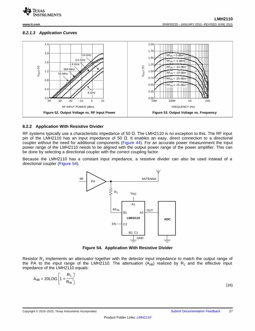
8.2.1.3 Application Curves
Figure 52. Output Voltage vs. RF Input Power Figure 53. Output Voltage vs. Frequency
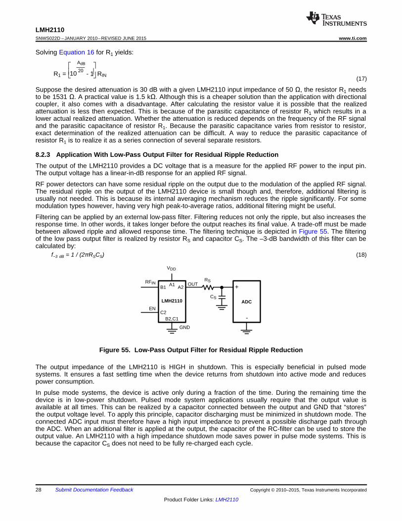
8.2.2 Application With Resistive DividerRF systems typically use a characteristic impedance of 50 Ω. The LMH2110 is no exception to this. The RF inputpin of the LMH2110 has an input impedance of 50 Ω. It enables an easy, direct connection to a directionalcoupler without the need for additional components (Figure 44). For an accurate power measurement the inputpower range of the LMH2110 needs to be aligned with the output power range of the power amplifier. This canbe done by selecting a directional coupler with the correct coupling factor.
Because the LMH2110 has a constant input impedance, a resistive divider can also be used instead of adirectional coupler (Figure 54).
Figure 54. Application With Resistive Divider
Resistor R1 implements an attenuator together with the detector input impedance to match the output range ofthe PA to the input range of the LMH2110. The attenuation (AdB) realized by R1 and the effective inputimpedance of the LMH2110 equals:
(16)
Copyright © 2010–2015, Texas Instruments Incorporated Submit Documentation Feedback 27
Product Folder Links: LMH2110
RFIN OUT
LMH2110
VDD
GND
ENADC
B1
CS
RSA1 A2
B2,C1C2
-
+
10R1 = - 1 RIN»¼
º«¬
ªAdB
20
LMH2110SNWS022D –JANUARY 2010–REVISED JUNE 2015 www.ti.com
Solving Equation 16 for R1 yields:
(17)
Suppose the desired attenuation is 30 dB with a given LMH2110 input impedance of 50 Ω, the resistor R1 needsto be 1531 Ω. A practical value is 1.5 kΩ. Although this is a cheaper solution than the application with directionalcoupler, it also comes with a disadvantage. After calculating the resistor value it is possible that the realizedattenuation is less then expected. This is because of the parasitic capacitance of resistor R1 which results in alower actual realized attenuation. Whether the attenuation is reduced depends on the frequency of the RF signaland the parasitic capacitance of resistor R1. Because the parasitic capacitance varies from resistor to resistor,exact determination of the realized attenuation can be difficult. A way to reduce the parasitic capacitance ofresistor R1 is to realize it as a series connection of several separate resistors.
8.2.3 Application With Low-Pass Output Filter for Residual Ripple ReductionThe output of the LMH2110 provides a DC voltage that is a measure for the applied RF power to the input pin.The output voltage has a linear-in-dB response for an applied RF signal.
RF power detectors can have some residual ripple on the output due to the modulation of the applied RF signal.The residual ripple on the output of the LMH2110 device is small though and, therefore, additional filtering isusually not needed. This is because its internal averaging mechanism reduces the ripple significantly. For somemodulation types however, having very high peak-to-average ratios, additional filtering might be useful.
Filtering can be applied by an external low-pass filter. Filtering reduces not only the ripple, but also increases theresponse time. In other words, it takes longer before the output reaches its final value. A trade-off must be madebetween allowed ripple and allowed response time. The filtering technique is depicted in Figure 55. The filteringof the low pass output filter is realized by resistor RS and capacitor CS. The –3-dB bandwidth of this filter can becalculated by:
f−3 dB = 1 / (2πRSCS) (18)
Figure 55. Low-Pass Output Filter for Residual Ripple Reduction
The output impedance of the LMH2110 is HIGH in shutdown. This is especially beneficial in pulsed modesystems. It ensures a fast settling time when the device returns from shutdown into active mode and reducespower consumption.
In pulse mode systems, the device is active only during a fraction of the time. During the remaining time thedevice is in low-power shutdown. Pulsed mode system applications usually require that the output value isavailable at all times. This can be realized by a capacitor connected between the output and GND that “stores”the output voltage level. To apply this principle, capacitor discharging must be minimized in shutdown mode. Theconnected ADC input must therefore have a high input impedance to prevent a possible discharge path throughthe ADC. When an additional filter is applied at the output, the capacitor of the RC-filter can be used to store theoutput value. An LMH2110 with a high impedance shutdown mode saves power in pulse mode systems. This isbecause the capacitor CS does not need to be fully re-charged each cycle.
28 Submit Documentation Feedback Copyright © 2010–2015, Texas Instruments Incorporated
Product Folder Links: LMH2110
LMH2110www.ti.com SNWS022D –JANUARY 2010–REVISED JUNE 2015
9 Power Supply RecommendationsThe LMH2110 is designed to operate from an input voltage supply range between 2.7 V to 5 V. This inputvoltage must be well regulated. Enable voltage levels lower than 400 mV below GND could lead to incorrectoperation of the device. Also, the resistance of the input supply rail must be low enough to ensure correctoperation of the device.
10 Layout
10.1 Layout GuidelinesAs with any other RF device, pay close careful attention to the board layout. If the board layout is not properlydesigned, performance might be less then can be expected for the application.
The LMH2110 is designed to be used in RF applications, having a characteristic impedance of 50 Ω. To achievethis impedance, the input of the LMH2110 needs to be connected via a 50-Ω transmission line. Transmissionlines can be created on PCBs using microstrip or (grounded) coplanar waveguide (GCPW) configurations.
In order to minimize injection of RF interference into the LMH2110 through the supply lines, the PCB traces forVDD and GND must be minimized for RF signals. This can be done by placing a small decoupling capacitorbetween the VDD and GND. It must be placed as close as possible to the VDD and GND pins of the LMH2110.
10.2 Layout Example
Figure 56. LMH2110 Layout
Copyright © 2010–2015, Texas Instruments Incorporated Submit Documentation Feedback 29
Product Folder Links: LMH2110

LMH2110SNWS022D –JANUARY 2010–REVISED JUNE 2015 www.ti.com
11 Device and Documentation Support
11.1 Community ResourcesThe following links connect to TI community resources. Linked contents are provided "AS IS" by the respectivecontributors. They do not constitute TI specifications and do not necessarily reflect TI's views; see TI's Terms ofUse.
TI E2E™ Online Community TI's Engineer-to-Engineer (E2E) Community. Created to foster collaborationamong engineers. At e2e.ti.com, you can ask questions, share knowledge, explore ideas and helpsolve problems with fellow engineers.
Design Support TI's Design Support Quickly find helpful E2E forums along with design support tools andcontact information for technical support.
11.2 TrademarksE2E is a trademark of Texas Instruments.All other trademarks are the property of their respective owners.
11.3 Electrostatic Discharge CautionThese devices have limited built-in ESD protection. The leads should be shorted together or the device placed in conductive foamduring storage or handling to prevent electrostatic damage to the MOS gates.
11.4 GlossarySLYZ022 — TI Glossary.
This glossary lists and explains terms, acronyms, and definitions.
12 Mechanical, Packaging, and Orderable InformationThe following pages include mechanical, packaging, and orderable information. This information is the mostcurrent data available for the designated devices. This data is subject to change without notice and revision ofthis document. For browser-based versions of this data sheet, refer to the left-hand navigation.
30 Submit Documentation Feedback Copyright © 2010–2015, Texas Instruments Incorporated
Product Folder Links: LMH2110
PACKAGE OPTION ADDENDUM
www.ti.com 8-Apr-2015
Addendum-Page 1
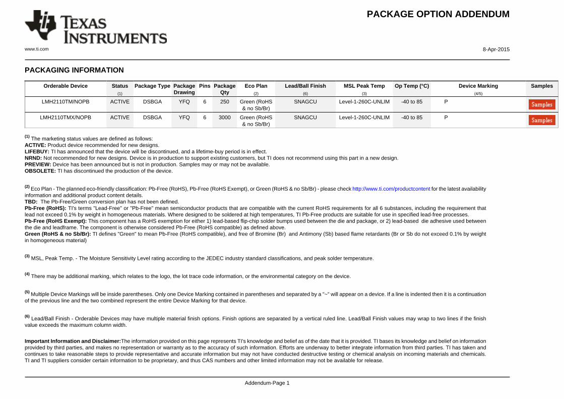
PACKAGING INFORMATION
Orderable Device Status(1)
Package Type PackageDrawing
Pins PackageQty
Eco Plan(2)
Lead/Ball Finish(6)
MSL Peak Temp(3)
Op Temp (°C) Device Marking(4/5)
Samples
LMH2110TM/NOPB ACTIVE DSBGA YFQ 6 250 Green (RoHS& no Sb/Br)
SNAGCU Level-1-260C-UNLIM -40 to 85 P
LMH2110TMX/NOPB ACTIVE DSBGA YFQ 6 3000 Green (RoHS& no Sb/Br)
SNAGCU Level-1-260C-UNLIM -40 to 85 P
(1) The marketing status values are defined as follows:ACTIVE: Product device recommended for new designs.LIFEBUY: TI has announced that the device will be discontinued, and a lifetime-buy period is in effect.NRND: Not recommended for new designs. Device is in production to support existing customers, but TI does not recommend using this part in a new design.PREVIEW: Device has been announced but is not in production. Samples may or may not be available.OBSOLETE: TI has discontinued the production of the device.
(2) Eco Plan - The planned eco-friendly classification: Pb-Free (RoHS), Pb-Free (RoHS Exempt), or Green (RoHS & no Sb/Br) - please check http://www.ti.com/productcontent for the latest availabilityinformation and additional product content details.TBD: The Pb-Free/Green conversion plan has not been defined.Pb-Free (RoHS): TI's terms "Lead-Free" or "Pb-Free" mean semiconductor products that are compatible with the current RoHS requirements for all 6 substances, including the requirement thatlead not exceed 0.1% by weight in homogeneous materials. Where designed to be soldered at high temperatures, TI Pb-Free products are suitable for use in specified lead-free processes.Pb-Free (RoHS Exempt): This component has a RoHS exemption for either 1) lead-based flip-chip solder bumps used between the die and package, or 2) lead-based die adhesive used betweenthe die and leadframe. The component is otherwise considered Pb-Free (RoHS compatible) as defined above.Green (RoHS & no Sb/Br): TI defines "Green" to mean Pb-Free (RoHS compatible), and free of Bromine (Br) and Antimony (Sb) based flame retardants (Br or Sb do not exceed 0.1% by weightin homogeneous material)
(3) MSL, Peak Temp. - The Moisture Sensitivity Level rating according to the JEDEC industry standard classifications, and peak solder temperature.
(4) There may be additional marking, which relates to the logo, the lot trace code information, or the environmental category on the device.
(5) Multiple Device Markings will be inside parentheses. Only one Device Marking contained in parentheses and separated by a "~" will appear on a device. If a line is indented then it is a continuationof the previous line and the two combined represent the entire Device Marking for that device.
(6) Lead/Ball Finish - Orderable Devices may have multiple material finish options. Finish options are separated by a vertical ruled line. Lead/Ball Finish values may wrap to two lines if the finishvalue exceeds the maximum column width.
Important Information and Disclaimer:The information provided on this page represents TI's knowledge and belief as of the date that it is provided. TI bases its knowledge and belief on informationprovided by third parties, and makes no representation or warranty as to the accuracy of such information. Efforts are underway to better integrate information from third parties. TI has taken andcontinues to take reasonable steps to provide representative and accurate information but may not have conducted destructive testing or chemical analysis on incoming materials and chemicals.TI and TI suppliers consider certain information to be proprietary, and thus CAS numbers and other limited information may not be available for release.
PACKAGE OPTION ADDENDUM
www.ti.com 8-Apr-2015
Addendum-Page 2
In no event shall TI's liability arising out of such information exceed the total purchase price of the TI part(s) at issue in this document sold by TI to Customer on an annual basis.
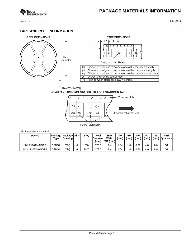
TAPE AND REEL INFORMATION
*All dimensions are nominal
Device PackageType
PackageDrawing
Pins SPQ ReelDiameter
(mm)
ReelWidth
W1 (mm)
A0(mm)
B0(mm)
K0(mm)
P1(mm)
W(mm)
Pin1Quadrant
LMH2110TM/NOPB DSBGA YFQ 6 250 178.0 8.4 1.04 1.4 0.76 4.0 8.0 Q1
LMH2110TMX/NOPB DSBGA YFQ 6 3000 178.0 8.4 1.04 1.4 0.76 4.0 8.0 Q1
PACKAGE MATERIALS INFORMATION
www.ti.com 18-Jan-2018
Pack Materials-Page 1
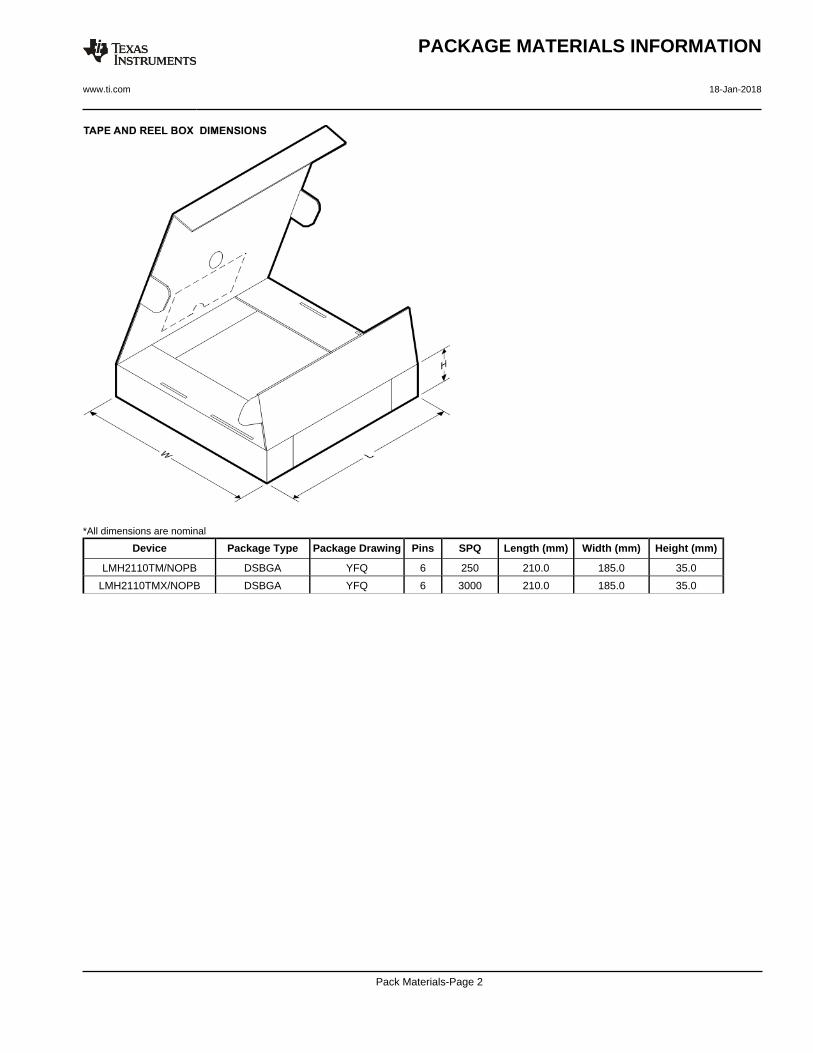
*All dimensions are nominal
Device Package Type Package Drawing Pins SPQ Length (mm) Width (mm) Height (mm)
LMH2110TM/NOPB DSBGA YFQ 6 250 210.0 185.0 35.0
LMH2110TMX/NOPB DSBGA YFQ 6 3000 210.0 185.0 35.0
PACKAGE MATERIALS INFORMATION
www.ti.com 18-Jan-2018
Pack Materials-Page 2
MECHANICAL DATA
YFQ0006xxx
www.ti.com
TMD06XXX (Rev B)
E
0.600±0.075
D
A. All linear dimensions are in millimeters. Dimensioning and tolerancing per ASME Y14.5M-1994.B. This drawing is subject to change without notice.
NOTES:
4215075/A 12/12
D: Max =
E: Max =
1.27 mm, Min =
0.87 mm, Min =
1.21 mm
0.81 mm
IMPORTANT NOTICE
Texas Instruments Incorporated (TI) reserves the right to make corrections, enhancements, improvements and other changes to itssemiconductor products and services per JESD46, latest issue, and to discontinue any product or service per JESD48, latest issue. Buyersshould obtain the latest relevant information before placing orders and should verify that such information is current and complete.TI’s published terms of sale for semiconductor products (http://www.ti.com/sc/docs/stdterms.htm) apply to the sale of packaged integratedcircuit products that TI has qualified and released to market. Additional terms may apply to the use or sale of other types of TI products andservices.Reproduction of significant portions of TI information in TI data sheets is permissible only if reproduction is without alteration and isaccompanied by all associated warranties, conditions, limitations, and notices. TI is not responsible or liable for such reproduceddocumentation. Information of third parties may be subject to additional restrictions. Resale of TI products or services with statementsdifferent from or beyond the parameters stated by TI for that product or service voids all express and any implied warranties for theassociated TI product or service and is an unfair and deceptive business practice. TI is not responsible or liable for any such statements.Buyers and others who are developing systems that incorporate TI products (collectively, “Designers”) understand and agree that Designersremain responsible for using their independent analysis, evaluation and judgment in designing their applications and that Designers havefull and exclusive responsibility to assure the safety of Designers' applications and compliance of their applications (and of all TI productsused in or for Designers’ applications) with all applicable regulations, laws and other applicable requirements. Designer represents that, withrespect to their applications, Designer has all the necessary expertise to create and implement safeguards that (1) anticipate dangerousconsequences of failures, (2) monitor failures and their consequences, and (3) lessen the likelihood of failures that might cause harm andtake appropriate actions. Designer agrees that prior to using or distributing any applications that include TI products, Designer willthoroughly test such applications and the functionality of such TI products as used in such applications.TI’s provision of technical, application or other design advice, quality characterization, reliability data or other services or information,including, but not limited to, reference designs and materials relating to evaluation modules, (collectively, “TI Resources”) are intended toassist designers who are developing applications that incorporate TI products; by downloading, accessing or using TI Resources in anyway, Designer (individually or, if Designer is acting on behalf of a company, Designer’s company) agrees to use any particular TI Resourcesolely for this purpose and subject to the terms of this Notice.TI’s provision of TI Resources does not expand or otherwise alter TI’s applicable published warranties or warranty disclaimers for TIproducts, and no additional obligations or liabilities arise from TI providing such TI Resources. TI reserves the right to make corrections,enhancements, improvements and other changes to its TI Resources. TI has not conducted any testing other than that specificallydescribed in the published documentation for a particular TI Resource.Designer is authorized to use, copy and modify any individual TI Resource only in connection with the development of applications thatinclude the TI product(s) identified in such TI Resource. NO OTHER LICENSE, EXPRESS OR IMPLIED, BY ESTOPPEL OR OTHERWISETO ANY OTHER TI INTELLECTUAL PROPERTY RIGHT, AND NO LICENSE TO ANY TECHNOLOGY OR INTELLECTUAL PROPERTYRIGHT OF TI OR ANY THIRD PARTY IS GRANTED HEREIN, including but not limited to any patent right, copyright, mask work right, orother intellectual property right relating to any combination, machine, or process in which TI products or services are used. Informationregarding or referencing third-party products or services does not constitute a license to use such products or services, or a warranty orendorsement thereof. Use of TI Resources may require a license from a third party under the patents or other intellectual property of thethird party, or a license from TI under the patents or other intellectual property of TI.TI RESOURCES ARE PROVIDED “AS IS” AND WITH ALL FAULTS. TI DISCLAIMS ALL OTHER WARRANTIES ORREPRESENTATIONS, EXPRESS OR IMPLIED, REGARDING RESOURCES OR USE THEREOF, INCLUDING BUT NOT LIMITED TOACCURACY OR COMPLETENESS, TITLE, ANY EPIDEMIC FAILURE WARRANTY AND ANY IMPLIED WARRANTIES OFMERCHANTABILITY, FITNESS FOR A PARTICULAR PURPOSE, AND NON-INFRINGEMENT OF ANY THIRD PARTY INTELLECTUALPROPERTY RIGHTS. TI SHALL NOT BE LIABLE FOR AND SHALL NOT DEFEND OR INDEMNIFY DESIGNER AGAINST ANY CLAIM,INCLUDING BUT NOT LIMITED TO ANY INFRINGEMENT CLAIM THAT RELATES TO OR IS BASED ON ANY COMBINATION OFPRODUCTS EVEN IF DESCRIBED IN TI RESOURCES OR OTHERWISE. IN NO EVENT SHALL TI BE LIABLE FOR ANY ACTUAL,DIRECT, SPECIAL, COLLATERAL, INDIRECT, PUNITIVE, INCIDENTAL, CONSEQUENTIAL OR EXEMPLARY DAMAGES INCONNECTION WITH OR ARISING OUT OF TI RESOURCES OR USE THEREOF, AND REGARDLESS OF WHETHER TI HAS BEENADVISED OF THE POSSIBILITY OF SUCH DAMAGES.Unless TI has explicitly designated an individual product as meeting the requirements of a particular industry standard (e.g., ISO/TS 16949and ISO 26262), TI is not responsible for any failure to meet such industry standard requirements.Where TI specifically promotes products as facilitating functional safety or as compliant with industry functional safety standards, suchproducts are intended to help enable customers to design and create their own applications that meet applicable functional safety standardsand requirements. Using products in an application does not by itself establish any safety features in the application. Designers mustensure compliance with safety-related requirements and standards applicable to their applications. Designer may not use any TI products inlife-critical medical equipment unless authorized officers of the parties have executed a special contract specifically governing such use.Life-critical medical equipment is medical equipment where failure of such equipment would cause serious bodily injury or death (e.g., lifesupport, pacemakers, defibrillators, heart pumps, neurostimulators, and implantables). Such equipment includes, without limitation, allmedical devices identified by the U.S. Food and Drug Administration as Class III devices and equivalent classifications outside the U.S.TI may expressly designate certain products as completing a particular qualification (e.g., Q100, Military Grade, or Enhanced Product).Designers agree that it has the necessary expertise to select the product with the appropriate qualification designation for their applicationsand that proper product selection is at Designers’ own risk. Designers are solely responsible for compliance with all legal and regulatoryrequirements in connection with such selection.Designer will fully indemnify TI and its representatives against any damages, costs, losses, and/or liabilities arising out of Designer’s non-compliance with the terms and provisions of this Notice.
Mailing Address: Texas Instruments, Post Office Box 655303, Dallas, Texas 75265Copyright © 2018, Texas Instruments Incorporated