Embed Size (px)
Citation preview
VIN
VOUT
V+
+
-+
-
V+
C = 200pFSAMPLECLOCK
Copyright © 2016, Texas Instruments Incorporated
Product
Folder
Order
Now
Technical
Documents
Tools &
Software
Support &Community
An IMPORTANT NOTICE at the end of this data sheet addresses availability, warranty, changes, use in safety-critical applications,intellectual property matters and other important disclaimers. PRODUCTION DATA.
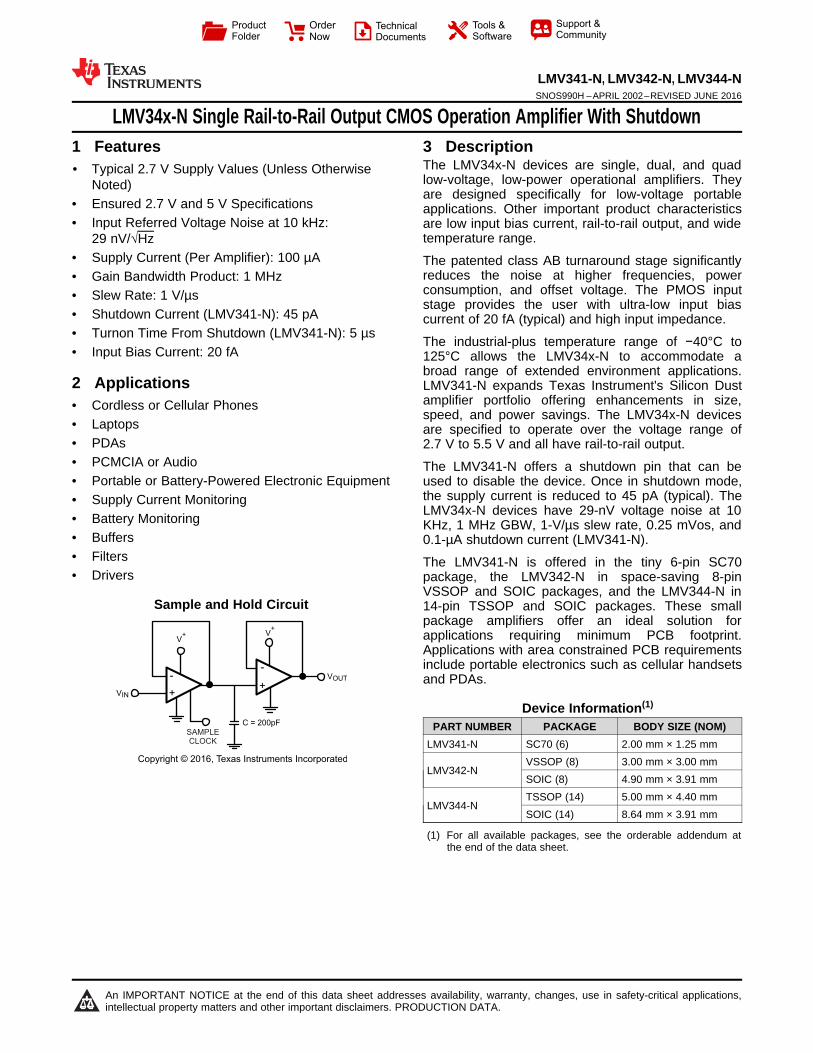
LMV341-N, LMV342-N, LMV344-NSNOS990H –APRIL 2002–REVISED JUNE 2016
LMV34x-N Single Rail-to-Rail Output CMOS Operation Amplifier With Shutdown
1
1 Features1• Typical 2.7 V Supply Values (Unless Otherwise
Noted)• Ensured 2.7 V and 5 V Specifications• Input Referred Voltage Noise at 10 kHz:
29 nV/√Hz• Supply Current (Per Amplifier): 100 µA• Gain Bandwidth Product: 1 MHz• Slew Rate: 1 V/µs• Shutdown Current (LMV341-N): 45 pA• Turnon Time From Shutdown (LMV341-N): 5 µs• Input Bias Current: 20 fA
2 Applications• Cordless or Cellular Phones• Laptops• PDAs• PCMCIA or Audio• Portable or Battery-Powered Electronic Equipment• Supply Current Monitoring• Battery Monitoring• Buffers• Filters• Drivers
Sample and Hold Circuit
3 DescriptionThe LMV34x-N devices are single, dual, and quadlow-voltage, low-power operational amplifiers. Theyare designed specifically for low-voltage portableapplications. Other important product characteristicsare low input bias current, rail-to-rail output, and widetemperature range.
The patented class AB turnaround stage significantlyreduces the noise at higher frequencies, powerconsumption, and offset voltage. The PMOS inputstage provides the user with ultra-low input biascurrent of 20 fA (typical) and high input impedance.
The industrial-plus temperature range of −40°C to125°C allows the LMV34x-N to accommodate abroad range of extended environment applications.LMV341-N expands Texas Instrument's Silicon Dustamplifier portfolio offering enhancements in size,speed, and power savings. The LMV34x-N devicesare specified to operate over the voltage range of2.7 V to 5.5 V and all have rail-to-rail output.
The LMV341-N offers a shutdown pin that can beused to disable the device. Once in shutdown mode,the supply current is reduced to 45 pA (typical). TheLMV34x-N devices have 29-nV voltage noise at 10KHz, 1 MHz GBW, 1-V/µs slew rate, 0.25 mVos, and0.1-µA shutdown current (LMV341-N).
The LMV341-N is offered in the tiny 6-pin SC70package, the LMV342-N in space-saving 8-pinVSSOP and SOIC packages, and the LMV344-N in14-pin TSSOP and SOIC packages. These smallpackage amplifiers offer an ideal solution forapplications requiring minimum PCB footprint.Applications with area constrained PCB requirementsinclude portable electronics such as cellular handsetsand PDAs.
Device Information(1)
PART NUMBER PACKAGE BODY SIZE (NOM)LMV341-N SC70 (6) 2.00 mm × 1.25 mm
LMV342-NVSSOP (8) 3.00 mm × 3.00 mmSOIC (8) 4.90 mm × 3.91 mm
LMV344-NTSSOP (14) 5.00 mm × 4.40 mmSOIC (14) 8.64 mm × 3.91 mm
(1) For all available packages, see the orderable addendum atthe end of the data sheet.
2
LMV341-N, LMV342-N, LMV344-NSNOS990H –APRIL 2002–REVISED JUNE 2016 www.ti.com
Product Folder Links: LMV341-N LMV342-N LMV344-N
Submit Documentation Feedback Copyright © 2002–2016, Texas Instruments Incorporated
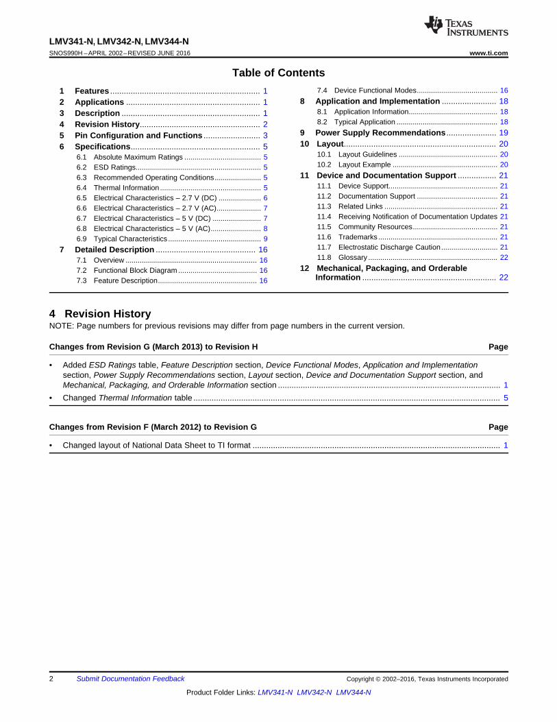
Table of Contents1 Features .................................................................. 12 Applications ........................................................... 13 Description ............................................................. 14 Revision History..................................................... 25 Pin Configuration and Functions ......................... 36 Specifications......................................................... 5
6.1 Absolute Maximum Ratings ...................................... 56.2 ESD Ratings.............................................................. 56.3 Recommended Operating Conditions....................... 56.4 Thermal Information .................................................. 56.5 Electrical Characteristics – 2.7 V (DC) ..................... 66.6 Electrical Characteristics – 2.7 V (AC)...................... 76.7 Electrical Characteristics – 5 V (DC) ........................ 76.8 Electrical Characteristics – 5 V (AC)......................... 86.9 Typical Characteristics .............................................. 9
7 Detailed Description ............................................ 167.1 Overview ................................................................. 167.2 Functional Block Diagram ....................................... 167.3 Feature Description................................................. 16
7.4 Device Functional Modes........................................ 168 Application and Implementation ........................ 18
8.1 Application Information............................................ 188.2 Typical Application .................................................. 18
9 Power Supply Recommendations ...................... 1910 Layout................................................................... 20
10.1 Layout Guidelines ................................................. 2010.2 Layout Example .................................................... 20
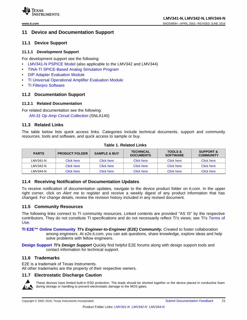
11 Device and Documentation Support ................. 2111.1 Device Support...................................................... 2111.2 Documentation Support ........................................ 2111.3 Related Links ........................................................ 2111.4 Receiving Notification of Documentation Updates 2111.5 Community Resources.......................................... 2111.6 Trademarks ........................................................... 2111.7 Electrostatic Discharge Caution............................ 2111.8 Glossary ................................................................ 22
12 Mechanical, Packaging, and OrderableInformation ........................................................... 22
4 Revision HistoryNOTE: Page numbers for previous revisions may differ from page numbers in the current version.
Changes from Revision G (March 2013) to Revision H Page
• Added ESD Ratings table, Feature Description section, Device Functional Modes, Application and Implementationsection, Power Supply Recommendations section, Layout section, Device and Documentation Support section, andMechanical, Packaging, and Orderable Information section .................................................................................................. 1
• Changed Thermal Information table ....................................................................................................................................... 5
Changes from Revision F (March 2012) to Revision G Page
• Changed layout of National Data Sheet to TI format ............................................................................................................. 1

V+
OUT
+IN
GND
-IN
6
4
1
2
3
+
-
SHDN5
3
LMV341-N, LMV342-N, LMV344-Nwww.ti.com SNOS990H –APRIL 2002–REVISED JUNE 2016
Product Folder Links: LMV341-N LMV342-N LMV344-N
Submit Documentation FeedbackCopyright © 2002–2016, Texas Instruments Incorporated
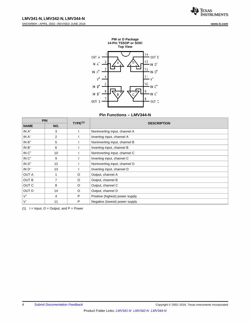
5 Pin Configuration and Functions
DCK Package6-Pin SC70Top View
(1) I = Input, O = Output, and P = Power
Pin Functions – LMV341-NPIN
TYPE (1) DESCRIPTIONNAME NO.+IN 1 I Noninverting input–IN 3 I Inverting inputGND 2 P Negative supply inputOUT 4 O OutputV+ 6 P Positive supply inputSHDN 5 I Active low enable input
DGK or D Package8-Pin VSSOP or SOIC
Top View
(1) I = Input, O = Output, and P = Power
Pin Functions – LMV342-NPIN
TYPE (1) DESCRIPTIONNAME NO.IN A+ 3 I Noninverting input, channel AIN A– 2 I Inverting input, channel AIN B+ 5 I Noninverting input, channel BIN B– 6 I Inverting input, channel BOUT A 1 O Output, channel AOUT B 7 O Output, channel BV+ 8 P Positive (highest) power supplyV– 4 P Negative (lowest) power supply
4
LMV341-N, LMV342-N, LMV344-NSNOS990H –APRIL 2002–REVISED JUNE 2016 www.ti.com
Product Folder Links: LMV341-N LMV342-N LMV344-N
Submit Documentation Feedback Copyright © 2002–2016, Texas Instruments Incorporated
PW or D Package14-Pin TSSOP or SOIC
Top View
(1) I = Input, O = Output, and P = Power
Pin Functions – LMV344-NPIN
TYPE (1) DESCRIPTIONNAME NO.IN A+ 3 I Noninverting input, channel AIN A– 2 I Inverting input, channel AIN B+ 5 I Noninverting input, channel BIN B– 6 I Inverting input, channel BIN C+ 10 I Noninverting input, channel CIN C– 9 I Inverting input, channel CIN D+ 12 I Noninverting input, channel DIN D– 13 I Inverting input, channel DOUT A 1 O Output, channel AOUT B 7 O Output, channel BOUT C 8 O Output, channel COUT D 14 O Output, channel DV+ 4 P Positive (highest) power supplyV– 11 P Negative (lowest) power supply

5
LMV341-N, LMV342-N, LMV344-Nwww.ti.com SNOS990H –APRIL 2002–REVISED JUNE 2016
Product Folder Links: LMV341-N LMV342-N LMV344-N
Submit Documentation FeedbackCopyright © 2002–2016, Texas Instruments Incorporated
(1) Stresses beyond those listed under Absolute Maximum Ratings may cause permanent damage to the device. These are stress ratingsonly, which do not imply functional operation of the device at these or any other conditions beyond those indicated under RecommendedOperating Conditions. Exposure to absolute-maximum-rated conditions for extended periods may affect device reliability.
(2) If Military/Aerospace specified devices are required, please contact the Texas Instruments Sales Office/Distributors for availability andspecifications.
(3) Shorting output to V+ will adversely affect reliability.(4) Shorting output to V- will adversely affect reliability.(5) The maximum power dissipation is a function of TJ(MAX), RθJA. The maximum allowable power dissipation at any ambient temperature is
PD = (TJ(MAX) – TA) / RθJA. All numbers apply for packages soldered directly onto a PCB.
6 Specifications
6.1 Absolute Maximum Ratingsover operating free-air temperature range (unless otherwise noted) (1) (2)
MIN MAX UNITDifferential input voltage ±Supply voltageSupply voltage (V + – V –) 6 VOutput short circuit to V + See (3)
Output short circuit to V – See (4)
Lead temperatureInfrared or convection reflow (20 s) 235
°CWave soldering (10 s) 260
Junction temperature, TJ(5) 150 °C
Storage temperature, Tstg –65 150 °C
(1) Human Body Model, applicable std. MIL-STD-883, Method 3015.7.(2) Machine Model, applicable std. JESD22-A115-A (ESD MM std. of JEDEC) Field-Induced Charge-Device Model, applicable std. JESD22-
C101-C (ESD FICDM std. of JEDEC).
6.2 ESD RatingsVALUE UNIT
V(ESD) Electrostatic dischargeHuman-body model (HBM) (1) ±2000
VMachine model (MM) (2) ±200
6.3 Recommended Operating Conditionsover operating free-air temperature range (unless otherwise noted)
MIN MAX UNITSupply voltage 2.7 5.5 VTemperature –40 125 °C
(1) For more information about traditional and new thermal metrics, see the Semiconductor and IC Package Thermal Metrics applicationreport.
6.4 Thermal Information
THERMAL METRIC (1)
LMV341-N LMV342-N LMV344-N
UNITDCK(SC70)
D(SOIC)
DGK(VSSOP)
D(SOIC)
PW(TSSOP)
6 PINS 8 PINS 8 PINS 14 PINS 14 PINSRθJA Junction-to-ambient thermal resistance 414 190 235 145 155 °C/WRθJC(top) Junction-to-case (top) thermal resistance 116.1 65.2 68.4 45.9 50.5 °C/WRθJB Junction-to-board thermal resistance 53.3 61.4 98.8 44.1 66.2 °C/W
ψJTJunction-to-top characterizationparameter 8.8 16.1 9.8 10.2 6.3 °C/W
ψJBJunction-to-board characterizationparameter 52.7 60.8 97.3 43.7 65.6 °C/W
RθJC(bot)Junction-to-case (bottom) thermalresistance — — — — — °C/W
6
LMV341-N, LMV342-N, LMV344-NSNOS990H –APRIL 2002–REVISED JUNE 2016 www.ti.com
Product Folder Links: LMV341-N LMV342-N LMV344-N
Submit Documentation Feedback Copyright © 2002–2016, Texas Instruments Incorporated
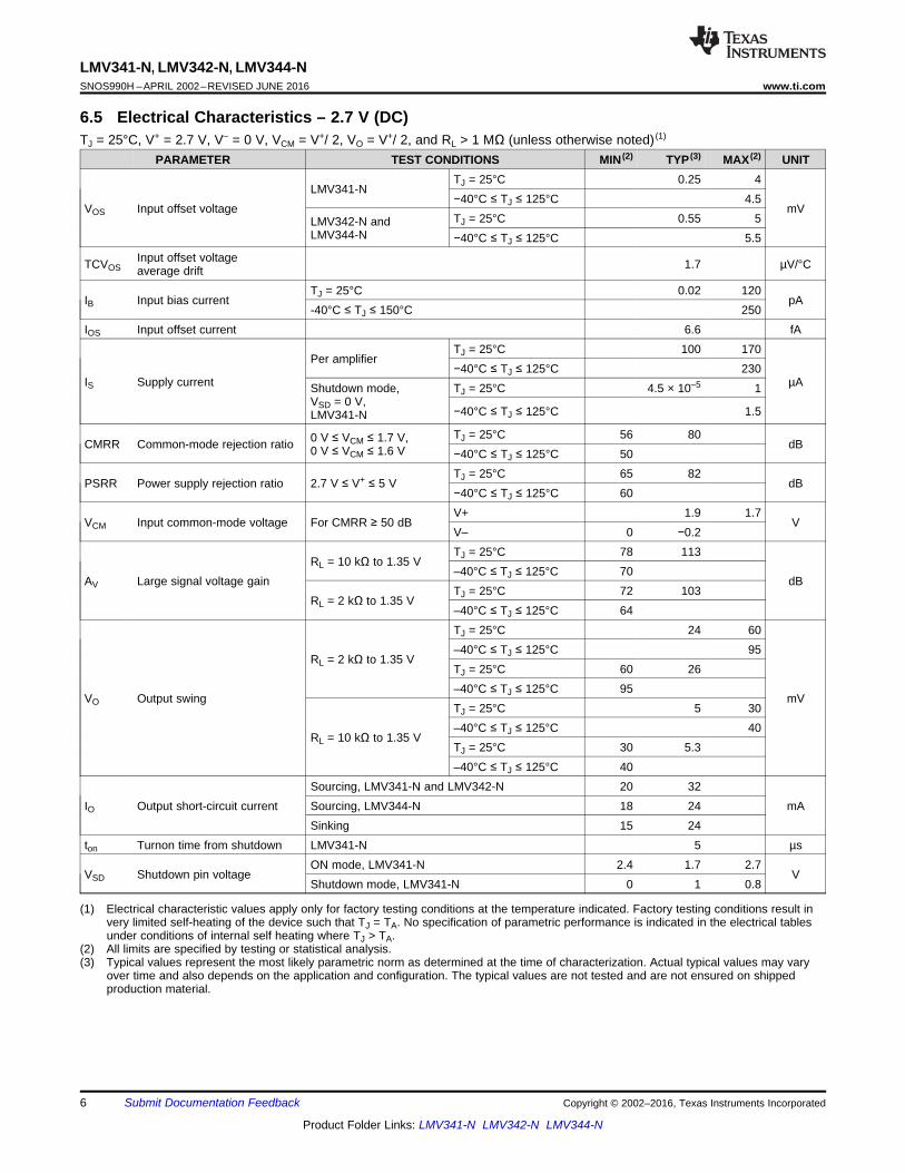
(1) Electrical characteristic values apply only for factory testing conditions at the temperature indicated. Factory testing conditions result invery limited self-heating of the device such that TJ = TA. No specification of parametric performance is indicated in the electrical tablesunder conditions of internal self heating where TJ > TA.
(2) All limits are specified by testing or statistical analysis.(3) Typical values represent the most likely parametric norm as determined at the time of characterization. Actual typical values may vary
over time and also depends on the application and configuration. The typical values are not tested and are not ensured on shippedproduction material.
6.5 Electrical Characteristics – 2.7 V (DC)TJ = 25°C, V+ = 2.7 V, V– = 0 V, VCM = V+/ 2, VO = V+/ 2, and RL > 1 MΩ (unless otherwise noted) (1)
PARAMETER TEST CONDITIONS MIN (2) TYP (3) MAX (2) UNIT
VOS Input offset voltageLMV341-N
TJ = 25°C 0.25 4
mV−40°C ≤ TJ ≤ 125°C 4.5
LMV342-N andLMV344-N
TJ = 25°C 0.55 5−40°C ≤ TJ ≤ 125°C 5.5
TCVOSInput offset voltageaverage drift 1.7 µV/°C
IB Input bias currentTJ = 25°C 0.02 120
pA-40°C ≤ TJ ≤ 150°C 250
IOS Input offset current 6.6 fA
IS Supply current
Per amplifierTJ = 25°C 100 170
µA−40°C ≤ TJ ≤ 125°C 230
Shutdown mode,VSD = 0 V,LMV341-N
TJ = 25°C 4.5 × 10⁻⁵ 1
−40°C ≤ TJ ≤ 125°C 1.5
CMRR Common-mode rejection ratio 0 V ≤ VCM ≤ 1.7 V,0 V ≤ VCM ≤ 1.6 V
TJ = 25°C 56 80dB
−40°C ≤ TJ ≤ 125°C 50
PSRR Power supply rejection ratio 2.7 V ≤ V+ ≤ 5 VTJ = 25°C 65 82
dB−40°C ≤ TJ ≤ 125°C 60
VCM Input common-mode voltage For CMRR ≥ 50 dBV+ 1.9 1.7
VV– 0 −0.2
AV Large signal voltage gainRL = 10 kΩ to 1.35 V
TJ = 25°C 78 113
dB–40°C ≤ TJ ≤ 125°C 70
RL = 2 kΩ to 1.35 VTJ = 25°C 72 103–40°C ≤ TJ ≤ 125°C 64
VO Output swing
RL = 2 kΩ to 1.35 V
TJ = 25°C 24 60
mV
–40°C ≤ TJ ≤ 125°C 95TJ = 25°C 60 26–40°C ≤ TJ ≤ 125°C 95
RL = 10 kΩ to 1.35 V
TJ = 25°C 5 30–40°C ≤ TJ ≤ 125°C 40TJ = 25°C 30 5.3–40°C ≤ TJ ≤ 125°C 40
IO Output short-circuit currentSourcing, LMV341-N and LMV342-N 20 32
mASourcing, LMV344-N 18 24Sinking 15 24
ton Turnon time from shutdown LMV341-N 5 µs
VSD Shutdown pin voltageON mode, LMV341-N 2.4 1.7 2.7
VShutdown mode, LMV341-N 0 1 0.8

7
LMV341-N, LMV342-N, LMV344-Nwww.ti.com SNOS990H –APRIL 2002–REVISED JUNE 2016
Product Folder Links: LMV341-N LMV342-N LMV344-N
Submit Documentation FeedbackCopyright © 2002–2016, Texas Instruments Incorporated
(1) Electrical characteristic values apply only for factory testing conditions at the temperature indicated. Factory testing conditions result invery limited self-heating of the device such that TJ = TA. No specification of parametric performance is indicated in the electrical tablesunder conditions of internal self heating where TJ > TA.
(2) All limits are specified by testing or statistical analysis.(3) Typical values represent the most likely parametric norm as determined at the time of characterization. Actual typical values may vary
over time and also depends on the application and configuration. The typical values are not tested and are not ensured on shippedproduction material.
(4) Connected as voltage follower with 2-VPP step input. Number specified is the slower of the positive and negative slew rates.
6.6 Electrical Characteristics – 2.7 V (AC)TJ = 25°C, V+ = 2.7V, V− = 0V, VCM = V+/ 2, VO = V+/ 2, and RL > 1 MΩ (unless otherwise noted) (1)
PARAMETER TEST CONDITIONS MIN (2) TYP (3) MAX (2) UNITSR Slew rate RL = 10 kΩ (4) 1 V/µsGBW Gain bandwidth product RL = 100 kΩ, CL = 200 pF 1 MHzΦm Phase margin RL = 100 kΩ 72 °Gm Gain margin RL = 100 kΩ 20 dBen Input-referred voltage noise f = 1 kHz 40 nV/√Hzin Input-referred current noise f = 1 kHz 0.001 pA/√Hz
THD Total harmonic distortion f = 1 kHz, AV = +1,RL = 600 Ω, VIN = 1VPP
0.017%
(1) Electrical characteristic values apply only for factory testing conditions at the temperature indicated. Factory testing conditions result invery limited self-heating of the device such that TJ = TA. No specification of parametric performance is indicated in the electrical tablesunder conditions of internal self heating where TJ > TA.
(2) All limits are specified by testing or statistical analysis.(3) Typical values represent the most likely parametric norm as determined at the time of characterization. Actual typical values may vary
over time and also depends on the application and configuration. The typical values are not tested and are not ensured on shippedproduction material.
(4) RL is connected to mid-supply. The output voltage is GND + 0.2 V ≤ VO ≤ V+– 0.2 V
6.7 Electrical Characteristics – 5 V (DC)TJ = 25°C, V+ = 5 V, V− = 0 V, VCM = V+/ 2, VO = V+/ 2, and R L > 1 MΩ (unless otherwise noted) (1)
PARAMETER TEST CONDITIONS MIN (2) TYP (3) MAX (2) UNIT
VOS Input offset voltageLMV341-N
TJ = 25°C 0.025 4
mV–40°C ≤ TJ ≤ 125°C 4.5
LMV342-N and LMV344-NTJ = 25°C 0.7 5–40°C ≤ TJ ≤ 125°C 5.5
TCVOSInput offset voltageaverage drift 1.9 µV/°C
IB Input bias currentTJ = 25°C 0.02 200
pA–40°C ≤ TJ ≤ 125°C 375
IOS Input offset current 6.6 fA
IS Supply current
Per amplifierTJ = 25°C 107 200
µA–40°C ≤ TJ ≤ 125°C 260
Shutdown mode,VSD = 0 V,LMV341-N
TJ = 25°C 0.033 1
–40°C ≤ TJ ≤ 125°C 1.5
CMRR Common-mode rejectionratio
0 V ≤ VCM ≤ 4 V,0 V ≤ VCM ≤ 3.9 V
TJ = 25°C 56 86dB
–40°C ≤ TJ ≤ 125°C 50
PSRR Power supply rejection ratio 2.7 V ≤ V+ ≤ 5 VTJ = 25°C 65 82
dB–40°C ≤ TJ ≤ 125°C 60
VCM Input common-mode voltage For CMRR ≥ 50 dBV+ 4.2 4
VV– 0 −0.2
AV Large signal voltage gain (4)
RL = 10 kΩ to 2.5 VTJ = 25°C 78 116
dB–40°C ≤ TJ ≤ 125°C 70
RL = 2 kΩ to 2.5 VTJ = 25°C 72 107–40°C ≤ TJ ≤ 125°C 64

8
LMV341-N, LMV342-N, LMV344-NSNOS990H –APRIL 2002–REVISED JUNE 2016 www.ti.com
Product Folder Links: LMV341-N LMV342-N LMV344-N
Submit Documentation Feedback Copyright © 2002–2016, Texas Instruments Incorporated
Electrical Characteristics – 5 V (DC) (continued)TJ = 25°C, V+ = 5 V, V− = 0 V, VCM = V+/ 2, VO = V+/ 2, and R L > 1 MΩ (unless otherwise noted)(1)
PARAMETER TEST CONDITIONS MIN (2) TYP (3) MAX (2) UNIT
VO Output swing
RL = 2 kΩ to 2.5 V
TJ = 25°C 32 60
mV
–40°C ≤ TJ ≤ 125°C 95TJ = 25°C 60 34–40°C ≤ TJ ≤ 125°C 95
RL = 10 kΩ to 2.5 V
TJ = 25°C 7 30–40°C ≤ TJ ≤ 125°C 40TJ = 25°C 30 7–40°C ≤ TJ ≤ 125°C 40
IO Output short-circuit currentSourcing 85 113
mASinking 50 75
ton Turnon time from shutdown LMV341-N 5 µs
VSD Shutdown pin voltageON mode, LMV341-N 4.5 3.1 5
VShutdown mode, LMV341-N 0 1 0.8
(1) Electrical characteristic values apply only for factory testing conditions at the temperature indicated. Factory testing conditions result invery limited self-heating of the device such that TJ = TA. No specification of parametric performance is indicated in the electrical tablesunder conditions of internal self heating where TJ > TA.
(2) All limits are specified by testing or statistical analysis.(3) Typical values represent the most likely parametric norm as determined at the time of characterization. Actual typical values may vary
over time and also depends on the application and configuration. The typical values are not tested and are not ensured on shippedproduction material.
(4) Connected as voltage follower with 2-VPP step input. Number specified is the slower of the positive and negative slew rates.
6.8 Electrical Characteristics – 5 V (AC)TJ = 25°C, V+ = 5 V, V− = 0 V, VCM = V+/ 2, VO = V+/ 2 and R L > 1 MΩ (unless otherwise noted) (1)
PARAMETER CONDITIONS MIN (2) TYP (3) MAX (2) UNITSR Slew rate RL = 10 kΩ (4) 1 V/µsGBW Gain-bandwidth product RL = 10 kΩ, CL = 200 pF 1 MHzΦm Phase margin RL = 100 kΩ 70 degGm Gain margin RL = 100 kΩ 20 dBen Input-referred voltage noise f = 1 kHz 39 nV/√Hzin Input-referred current noise f = 1 kHz 0.001 pA/√Hz
THD Total harmonic distortion f = 1 kHz, AV = +1,RL = 600 Ω, VIN = 1VPP
0.012%
0.001 0.01 0.1 1 100.01
0.1
1
10
100
I SO
UR
CE
(m
A)
OUTPUT VOLTAGE REFERENCED TO V+ (V)
VS = 5V
125°C85°C
-40°C
25°C
0.001 0.01 0.1 1 100.001
0.01
0.1
1
10
100
I SO
UR
CE
(m
A)
OUTPUT VOLTAGE REFERENCED TO V+ (V)
25°C
125°C
85°C
-40°CVS = 2.7 V
2.5 3 3.5 4 4.5 520
22
24
26
28
30
32
34
OU
TP
UT
VO
LTA
GE
FR
OM
S
UP
PLY
VO
LTA
GE
(m
V)
SUPPLY VOLTAGE (V)
RL = 2k:
NEGATIVE SWING
POSITIVE SWING
2.5 3 3.5 4 4.5 53.0
3.5
4.0
4.5
5.0
5.5
6.0
6.5
7.0
OU
TP
UT
VO
LTA
GE
FR
OM
S
UP
PLY
VO
LTA
GE
(m
V)
SUPPLY VOLTAGE (V)
RL = 10k:
NEGATIVE SWING
POSITIVE SWING
2.5 3 3.5 4 4.5 550
60
70
80
90
100
110
120
130
140
150
SU
PP
LY C
UR
RE
NT
(P
A)
SUPPLY VOLTAGE (V)
125°C85°C
25°C
-40°C
-40 -20 0 20 40 60 80 100 120 140.001
.01
.1
1
10
100
1000
INP
UT
CU
RR
EN
T (
pA)
TEMPERATURE (C°)
VS = 5 V
9
LMV341-N, LMV342-N, LMV344-Nwww.ti.com SNOS990H –APRIL 2002–REVISED JUNE 2016
Product Folder Links: LMV341-N LMV342-N LMV344-N
Submit Documentation FeedbackCopyright © 2002–2016, Texas Instruments Incorporated
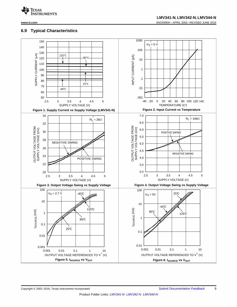
6.9 Typical Characteristics
Figure 1. Supply Current vs Supply Voltage (LMV341-N) Figure 2. Input Current vs Temperature
Figure 3. Output Voltage Swing vs Supply Voltage Figure 4. Output Voltage Swing vs Supply Voltage
Figure 5. ISOURCE vs VOUT Figure 6. ISOURCE vs VOUT

-1.5 -1 -0.5 0 0.5 1 1.5
OUTPUT VOLTAGE (V)
-300
-200
-100
0
100
200
300
INP
UT
VO
LTA
GE
(P
V)
VS = ±1.35V
RL = 10 k:
RL = 2 k:
-3 -2 -1 0 1 2 3
OUTPUT VOLTAGE (V)
-300
-200
-100
0
100
200
300
INP
UT
VO
LTA
GE
(P
V)
VS = ±2.5V
RL = 10 k:
RL = 2 k:
-0.2 0.5 1 1.5 2 2.5 3 3.5 4 4.5
VO
S (
mV
)
VCM (V)
0
0.5
1
1.5
2
2.5
3
VS = 5V -40°C
25°C
85°C
125°C
-0.2 0.3 0.8 1.3 1.8 2.30
0.5
1
1.5
2
2.5
3
VO
S (
mV
)
VCM (V)
VS = 2.7V
125°C
85°C
25°C
-40°C
0.001 0.01 0.1 1 100.001
0.01
0.1
1
10
100I S
INK
(m
A)
OUTPUT VOLTAGE REFERENCED TO V- (V)
VS = 2.7V -40°C
25°C
125°C
85°C
0.001 0.01 0.1 1 100.01
0.1
1
10
100
I SIN
K (
mA
)
OUTPUT VOLTAGE REFERENCED TO V- (V)
VS = 5V
125°C
25°C
85°C
-40°C
10
LMV341-N, LMV342-N, LMV344-NSNOS990H –APRIL 2002–REVISED JUNE 2016 www.ti.com
Product Folder Links: LMV341-N LMV342-N LMV344-N
Submit Documentation Feedback Copyright © 2002–2016, Texas Instruments Incorporated
Typical Characteristics (continued)
Figure 7. ISINK vs VOUT Figure 8. ISINK vs VOUT
Figure 9. VOS vs VCM Figure 10. VOS vs VCM
Figure 11. VIN vs VOUT Figure 12. VIN vs VOUT
-40 -20 0 20 40 60 80 100 120 1400
0.2
0.4
0.6
0.8
1
1.2
SLE
W R
AT
E (
V/P
s)
TEMPERATURE (°)
RISING EDGE
FALLING EDGE
AV = +1
RL = 10k:
VIN = 2VPP
VS = 2.7V
-40 -20 0 20 40 60 80 100 120 1400
0.2
0.4
0.6
0.8
1
1.2
SLE
W R
AT
E (
V/P
s)
TEMPERATURE (°)
RISING EDGE
FALLING EDGE
AV = +1
RL = 10k:
VIN = 2VPP
VS = 5V
2.5 3 3.5 4 4.5 50.5
0.6
0.7
0.8
0.9
1
1.1
1.2
1.3
1.4
1.5
SLE
W R
AT
E (
V/P
s)
SUPPLY VOLTAGE (V)
FALLING EDGE
RISING EDGE
AV = +1
RL = 10k:
VIN = 2VPP
10 100 1k 10k
FREQUENCY (Hz)
0
40
200
260
240220
80
60
20
120
140
160
180
100
INP
UT
VO
LTA
GE
NO
ISE
(nV
/H
z)
VS = 5V
VS = 2.7V
VCM = VS/2
100 1k 10k 100k 1M
FREQUENCY (Hz)
0
10
20
30
40
50
60
70
80C
MR
R (
dB
)
VIN = VS/2
RL = 5kΩ
VS = 2.7V
VS = 5V
100 10k 10M
FREQUENCY (Hz)
0
20
100
PS
RR
(dB
)
1M100k1k
90
50
10
80
60
40
30
70
RL = 5 k:
VS = 5 V, +PSRR
VS = 2.7 V, -PSRR
VS = 5 V, -PSRR
VS = 2.7 V, +PSRR
11
LMV341-N, LMV342-N, LMV344-Nwww.ti.com SNOS990H –APRIL 2002–REVISED JUNE 2016
Product Folder Links: LMV341-N LMV342-N LMV344-N
Submit Documentation FeedbackCopyright © 2002–2016, Texas Instruments Incorporated
Typical Characteristics (continued)
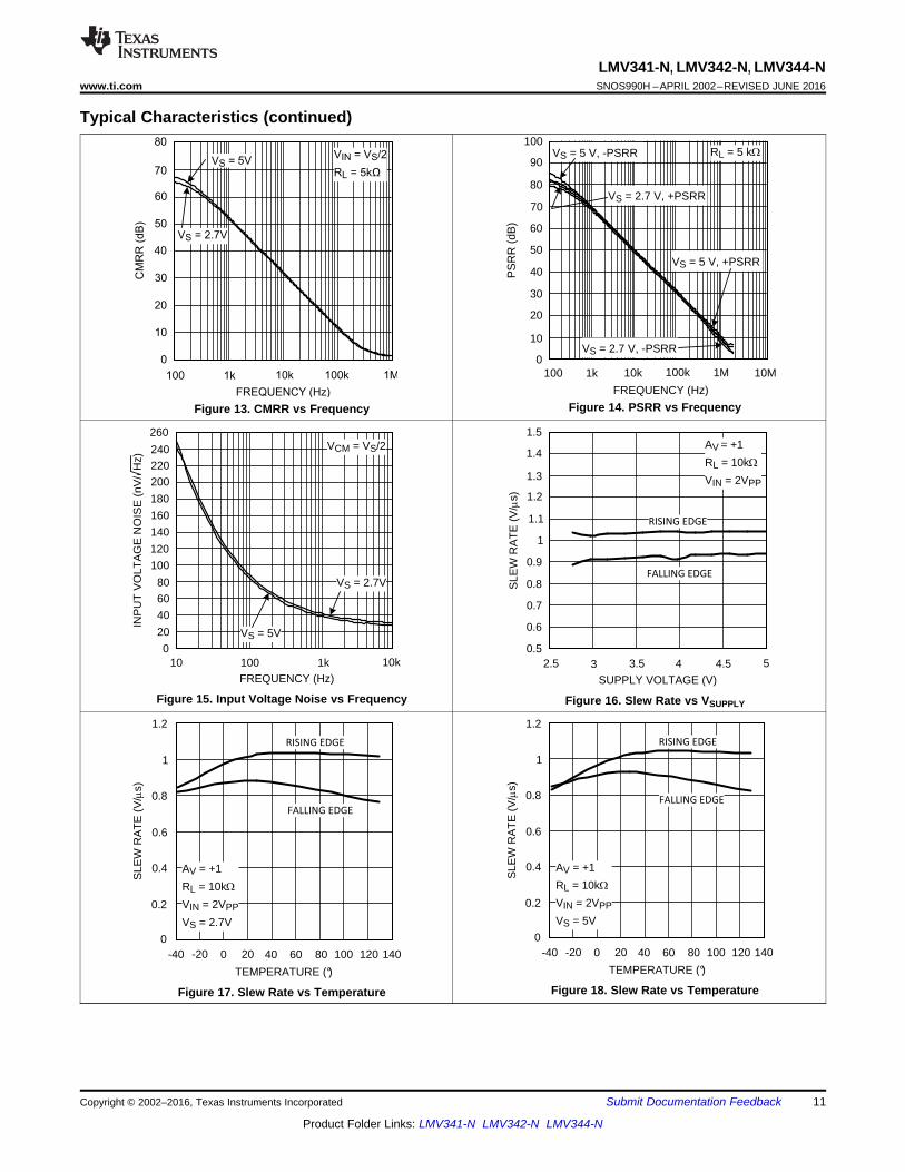
Figure 13. CMRR vs Frequency Figure 14. PSRR vs Frequency
Figure 15. Input Voltage Noise vs Frequency Figure 16. Slew Rate vs VSUPPLY
Figure 17. Slew Rate vs Temperature Figure 18. Slew Rate vs Temperature
1k 10k 100k 1M 10M
FREQUENCY (Hz)
-60
-40
-20
0
20
40
60
80
100
GA
IN (
dB)
PHASE
GAIN
-60
-40
-20
0
20
40
60
80
100
PH
AS
E
(°)
VS = 5V
RL = 600:
RL = 2k:
RL = 100k:
RL = 600:
RL = 2k:
RL = 100k:
1k 10k 100k 1M 10M
FREQUENCY (Hz)
-60
-40
-20
0
20
40
60
80
100
GA
IN (
dB)
PHASE
GAIN
VS = 5V
RL = 600:
CL = 1000pF
CL = 500pF
CL = 0
CL = 100pF
CL = 1000pF
CL = 500pF
CL = 100pFCL = 0
-60
-40
-20
0
20
40
60
80
100
PH
AS
E
(°)
1k 10k 100k 1M 10M
FREQUENCY (Hz)
-60
-40
-20
0
20
40
60
80
100
GA
IN (
dB)
PHASE
GAIN
-60
-40
-20
0
20
40
60
80
100
PH
AS
E
(°)
VS = 5V
RL = 2k:
125°C
25°C-40°C
125°C
-40°C
25°C
1k 10k 100k 1M 10M
FREQUENCY (Hz)
-60
-40
-20
0
20
40
60
80
100
GA
IN (
dB)
PHASE
GAIN
-60
-40
-20
0
20
40
60
80
100
PH
AS
E
(°)
VS = 2.7V
RL = 600:
RL = 2k:
RL = 100k:
RL = 600:
RL = 2k:
RL = 100k:
1 10 100 1k 100kFREQUENCY (Hz)
0.001
0.01
1
10T
HD
+N
(%
)
10k
0.1
AV = +10
AV = +1
VS = 2.7V, VO = 1VPP
VS = 5V, VO = 2.5VPP
VS = 2.7V, VO = 1VPP
VS = 5V, VO = 1VPP
0.00
10.0
10.1 1 10
VO (VPP)
0.01
0.1
1
10
TH
D+
N (
%)
f = 10KHz
RL = 600Ω
VS = 2.7V, AV = +10
VS = 5V, AV = +10
VS = 5V, AV =+1VS = 2.7V, AV = +1
12
LMV341-N, LMV342-N, LMV344-NSNOS990H –APRIL 2002–REVISED JUNE 2016 www.ti.com
Product Folder Links: LMV341-N LMV342-N LMV344-N
Submit Documentation Feedback Copyright © 2002–2016, Texas Instruments Incorporated
Typical Characteristics (continued)
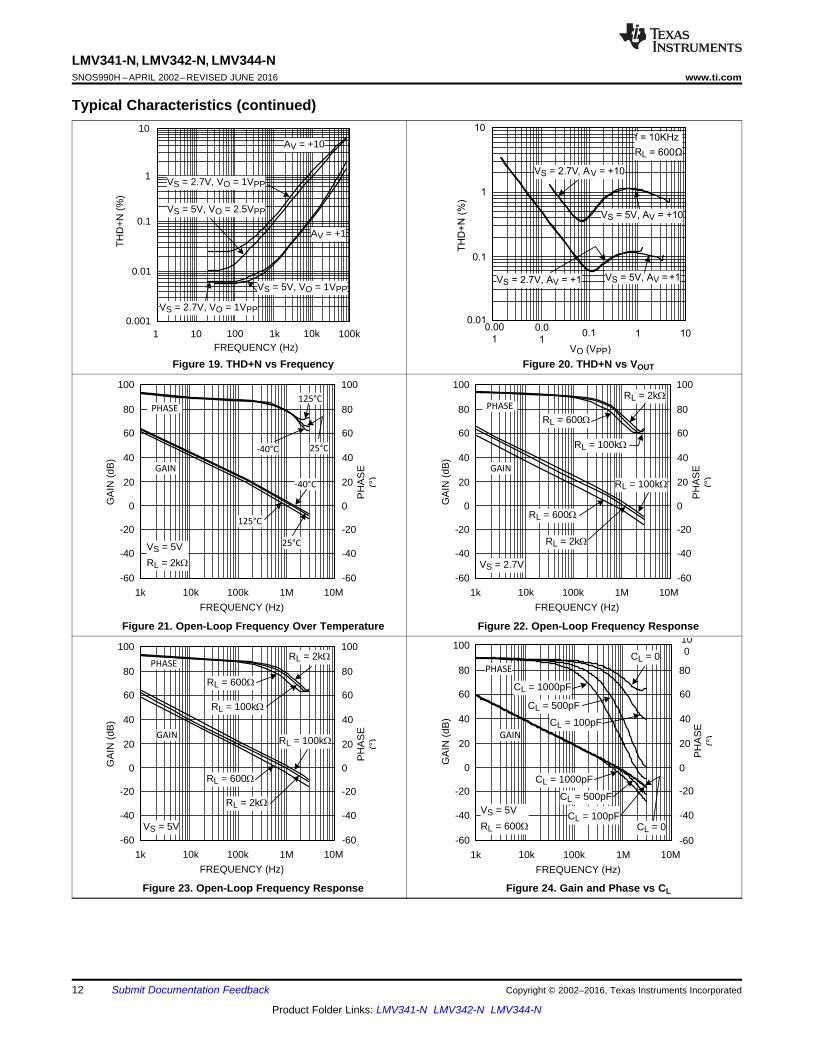
Figure 19. THD+N vs Frequency Figure 20. THD+N vs VOUT
Figure 21. Open-Loop Frequency Over Temperature Figure 22. Open-Loop Frequency Response
Figure 23. Open-Loop Frequency Response Figure 24. Gain and Phase vs CL
OU
TP
UT
SIG
NA
L
TIME (4 Ps/div)
INP
UT
SIG
NA
L
(1 V
/div
)
TA = 25°C
RL = 2k:
VS = ±2.5V
OU
TP
UT
SIG
NA
L
TIME (4 Ps/div)
INP
UT
SIG
NA
L
(50
mV
/div
)
TA = 125°C
RL = 2k:
VS = ±2.5V
-2.5 -2 -1.5 -1 -0.5 0 0.5 1 1.50
200
CA
PA
CIT
IVE
LO
AD
(pF
)
VO (V)
20
40
60
80
100
120
140
160
180VS = ±2.5
AV = +1
RL = 1M:
VO = 100mVPPO
UT
PU
T S
IGN
AL
TIME (4 Ps/div)
INP
UT
SIG
NA
L
(50
mV
/div
)
TA = 25°C
RL = 2k:
VS = ±2.5V
1k 10k 100k 1M 10M
FREQUENCY (Hz)
-60
-40
-20
0
20
40
60
80
100
GA
IN (
dB)
PHASE
GAIN
VS = 5V
RL = 100k:
CL = 1000pF
CL = 500pF
CL = 0
CL = 100pF
CL = 1000pF
CL = 500pF
CL = 100pF
CL = 0
-60
-40
-20
0
20
40
60
80
100
PH
AS
E
(°)
-2.5 -2 -1.5 -1 -0.5 0 0.5 1 1.5VO (V)
0
0.5
1
1.5
2
2.5
3
3.5
4
CA
PA
CIT
IVE
LO
AD
(nF
)
VS = ±2.5V
AV = +1
RL = 2k:
VO = 100mVPP
13
LMV341-N, LMV342-N, LMV344-Nwww.ti.com SNOS990H –APRIL 2002–REVISED JUNE 2016
Product Folder Links: LMV341-N LMV342-N LMV344-N
Submit Documentation FeedbackCopyright © 2002–2016, Texas Instruments Incorporated
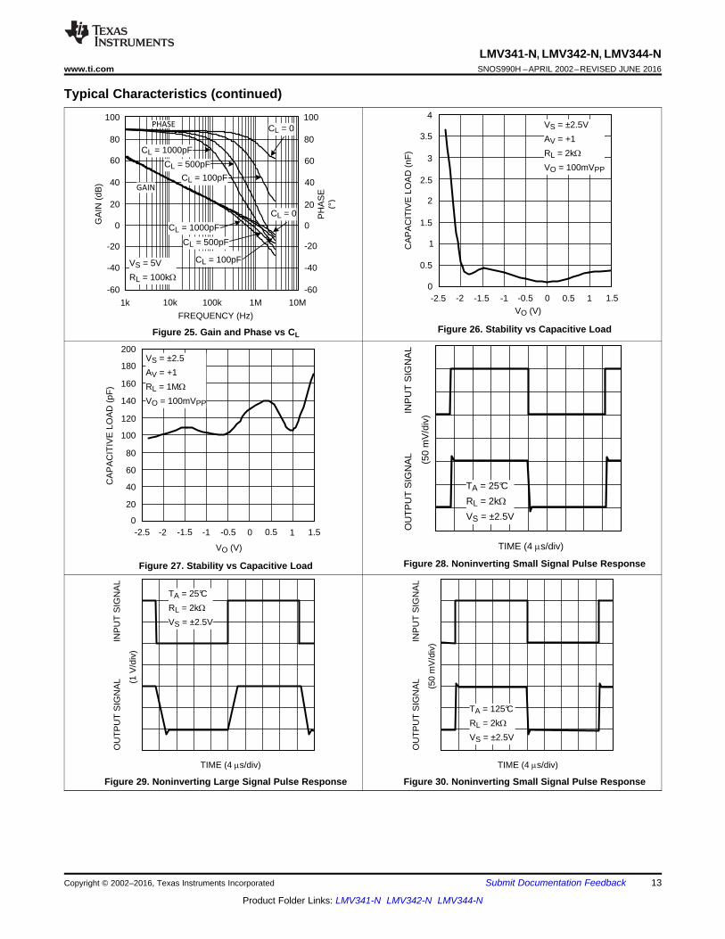
Typical Characteristics (continued)
Figure 25. Gain and Phase vs CL Figure 26. Stability vs Capacitive Load
Figure 27. Stability vs Capacitive Load Figure 28. Noninverting Small Signal Pulse Response
Figure 29. Noninverting Large Signal Pulse Response Figure 30. Noninverting Small Signal Pulse Response

OU
TP
UT
SIG
NA
L
TIME (4 Ps/div)
INP
UT
SIG
NA
L
(1 V
/div
)
TA = 25°C
RL = 2k:
VS = ±2.5V
OU
TP
UT
SIG
NA
L
TIME (4 Ps/div)
INP
UT
SIG
NA
L
(50 m
V/ d
iv)
TA = 125°C
RL = 2kΩ
VS = ±2.5V
OU
TP
UT
SIG
NA
L
TIME (4 Ps/div)
INP
UT
SIG
NA
L
(1 V
/div
)
TA = -40°C
RL = 2k:
VS = ±2.5V
OU
TP
UT
SIG
NA
L
TIME (4 Ps/div)
INP
UT
SIG
NA
L
(50 m
V/ d
iv)
TA = 25°C
RL = 2kΩ
VS = ±2.5V
OU
TP
UT
SIG
NA
L
TIME (4 Ps/div)
INP
UT
SIG
NA
L
(1 V
/div
)TA = 125°C
RL = 2k:
VS = ±2.5V
OU
TP
UT
SIG
NA
L
TIME (4 Ps/div)
INP
UT
SIG
NA
L
(50
mV
/div
)
TA = -40°C
RL = 2k:
VS = ±2.5V
14
LMV341-N, LMV342-N, LMV344-NSNOS990H –APRIL 2002–REVISED JUNE 2016 www.ti.com
Product Folder Links: LMV341-N LMV342-N LMV344-N
Submit Documentation Feedback Copyright © 2002–2016, Texas Instruments Incorporated
Typical Characteristics (continued)
Figure 31. Noninverting Large Signal Pulse Response Figure 32. Noninverting Small Signal Pulse Response
Figure 33. Noninverting Large Signal Pulse Response Figure 34. Inverting Small Signal Pulse Response
Figure 35. Inverting Large Signal Pulse Response Figure 36. Inverting Small Signal Pulse Response

100 1k 10k 100k 1M
FREQUENCY (Hz)
0
20
40
60
80
100
120
140
160
180
200
CR
OS
ST
ALK
RE
JEC
TIO
N (
dB)
VS = ±2.5V
OU
TP
UT
SIG
NA
L
TIME (4 Ps/div)
INP
UT
SIG
NA
L
(1 V
/div
)
TA = -40°C
RL = 2k:
VS = ±2.5V
OU
TP
UT
SIG
NA
L
TIME (4 Ps/div)
INP
UT
SIG
NA
L
(1 V
/div
)
TA = 125°C
RL = 2k:
VS = ±2.5V
OU
TP
UT
SIG
NA
L
TIME (4 Ps/div)
INP
UT
SIG
NA
L
(50 m
V/ d
iv)
TA = -40°C
RL = 2kΩ
VS = ±2.5V
15
LMV341-N, LMV342-N, LMV344-Nwww.ti.com SNOS990H –APRIL 2002–REVISED JUNE 2016
Product Folder Links: LMV341-N LMV342-N LMV344-N
Submit Documentation FeedbackCopyright © 2002–2016, Texas Instruments Incorporated
Typical Characteristics (continued)
Figure 37. Inverting Large Signal Pulse Response Figure 38. Inverting Small Signal Pulse Response
Figure 39. Inverting Large Signal Pulse Response Figure 40. Crosstalk Rejection vs Frequency

CLASS AB CONTROL
OUT
VDD
InP
InM
VEE
Copyright © 2016, Texas Instruments Incorporated
16
LMV341-N, LMV342-N, LMV344-NSNOS990H –APRIL 2002–REVISED JUNE 2016 www.ti.com
Product Folder Links: LMV341-N LMV342-N LMV344-N
Submit Documentation Feedback Copyright © 2002–2016, Texas Instruments Incorporated
7 Detailed Description
7.1 OverviewTI’s LMV34x-N family of amplifiers have 1-MHz bandwidth, 1-V/µs slew rate, a rail-to-rail output stage, andconsume only 100 µA of current per amplifier while active. When in shutdown mode it only consumes 45-pAsupply consumption with only 20 fA of input bias current. Lastly, these operational amplifiers provide an input-referred voltage noise 29 nV√Hz (at 10 kHz).
7.2 Functional Block Diagram
7.3 Feature Description
7.3.1 Class AB Turnaround Stage AmplifierThis patented folded cascode stage has a combined class AB amplifier stage, which replaces the conventionalfolded cascode stage. Therefore, the class AB folded cascode stage runs at a much lower quiescent currentcompared to conventional-folded cascode stages. This results in significantly smaller offset and noisecontributions. The reduced offset and noise contributions in turn reduce the offset voltage level and the voltagenoise level at the input of LMV34x-N. Also the lower quiescent current results in a high open-loop gain for theamplifier. The lower quiescent current does not affect the slew rate of the amplifier nor its ability to handle thetotal current swing coming from the input stage.
The input voltage noise of the device at low frequencies, below 1 kHz, is slightly higher than devices with a BJTinput stage; however, the PMOS input stage results in a much lower input bias current and the input voltagenoise drops at frequencies above 1 kHz.
7.4 Device Functional Modes
7.4.1 Shutdown FeatureThe LMV341-N is capable of being turned off to conserve power and increase battery life in portable devices.Once in shutdown mode the supply current is drastically reduced, 1-µA maximum, and the output is tri-stated.
The device is disabled when the shutdown pin voltage is pulled low. The shutdown pin must never be leftunconnected. Leaving the pin floating results in an undefined operation mode and the device may oscillatebetween shutdown and active modes.
The LMV341-N typically turns on 2.8 µs after the shutdown voltage is pulled high. The device turns off in lessthan 400 ns after shutdown voltage is pulled low. Figure 41 and Figure 42 show the turnon and turnoff time of theLMV341-N, respectively. To reduce the effect of the capacitance added to the circuit by the scope probe, in theturnoff time circuit a resistive load of 600 Ω is added. Figure 43 and Figure 44 show the test circuits used toobtain the two plots.

-0.5 0.5 1.5 2.5 3.5 4.5 5.5
VCM (V)
-200
-100
0
100
200
INP
UT
BIA
S (
fA)
VS = 5V
TA = 25°C
+
-
VIN = VS/2+-
VOUT
V+
SHDN
+
-
VIN = VS/2 +-
VOUT
V+
RL = 600:
SHDN
VO
UT
TIME (400 ns/div)
VS
HD
N
(1 V
/div
)
VS = 5V
VO
UT
TIME (1 Ps/div)
VS
HD
N
(1
V/d
iv)
RL = 600:
VS = 5V
17
LMV341-N, LMV342-N, LMV344-Nwww.ti.com SNOS990H –APRIL 2002–REVISED JUNE 2016
Product Folder Links: LMV341-N LMV342-N LMV344-N
Submit Documentation FeedbackCopyright © 2002–2016, Texas Instruments Incorporated
Device Functional Modes (continued)
Figure 41. Turnon Time Plot Figure 42. Turnoff Time Plot
Figure 43. Turnon Time Circuit Figure 44. Turnoff Time Circuit
7.4.2 Low Input Bias CurrentLMV34x-N amplifiers have a PMOS input stage. As a result, they have a much lower input bias current thandevices with BJT input stages. This feature makes these devices ideal for sensor circuits. A typical curve of theinput bias current of the LMV341-N is shown in Figure 45.
Figure 45. Input Bias Current vs VCM
VIN
VOUT
V+
+
-+
-
V+
C = 200pFSAMPLECLOCK
Copyright © 2016, Texas Instruments Incorporated
18
LMV341-N, LMV342-N, LMV344-NSNOS990H –APRIL 2002–REVISED JUNE 2016 www.ti.com
Product Folder Links: LMV341-N LMV342-N LMV344-N
Submit Documentation Feedback Copyright © 2002–2016, Texas Instruments Incorporated
8 Application and Implementation
NOTEInformation in the following applications sections is not part of the TI componentspecification, and TI does not warrant its accuracy or completeness. TI’s customers areresponsible for determining suitability of components for their purposes. Customers shouldvalidate and test their design implementation to confirm system functionality.
8.1 Application InformationThe LMV34x-N amplifier family features low voltage, low power, rail-to-rail output as well as a shutdowncapability, making it well suited for low voltage portable applications.
8.2 Typical Application
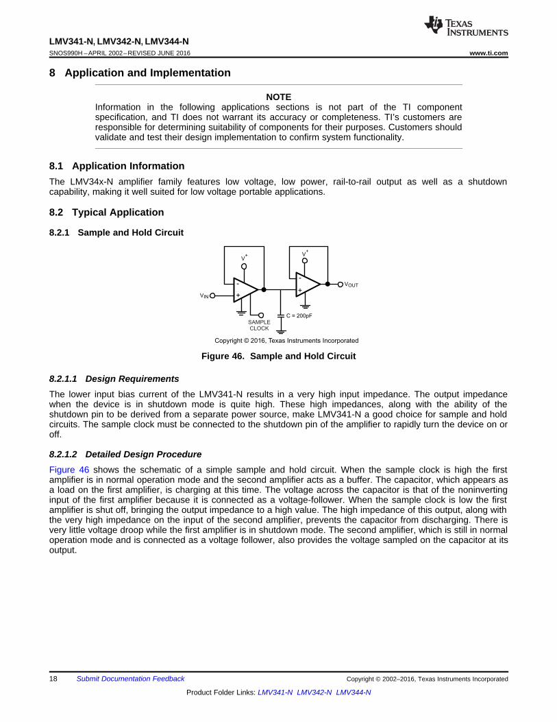
8.2.1 Sample and Hold Circuit
Figure 46. Sample and Hold Circuit
8.2.1.1 Design RequirementsThe lower input bias current of the LMV341-N results in a very high input impedance. The output impedancewhen the device is in shutdown mode is quite high. These high impedances, along with the ability of theshutdown pin to be derived from a separate power source, make LMV341-N a good choice for sample and holdcircuits. The sample clock must be connected to the shutdown pin of the amplifier to rapidly turn the device on oroff.
8.2.1.2 Detailed Design ProcedureFigure 46 shows the schematic of a simple sample and hold circuit. When the sample clock is high the firstamplifier is in normal operation mode and the second amplifier acts as a buffer. The capacitor, which appears asa load on the first amplifier, is charging at this time. The voltage across the capacitor is that of the noninvertinginput of the first amplifier because it is connected as a voltage-follower. When the sample clock is low the firstamplifier is shut off, bringing the output impedance to a high value. The high impedance of this output, along withthe very high impedance on the input of the second amplifier, prevents the capacitor from discharging. There isvery little voltage droop while the first amplifier is in shutdown mode. The second amplifier, which is still in normaloperation mode and is connected as a voltage follower, also provides the voltage sampled on the capacitor at itsoutput.

0 300 600 900 1200 1500
Sig
nalA
mplit
ude
Time (us)
Sample (5v/div)
Vin (1v/div)
Vout (1v/div)
C002
19
LMV341-N, LMV342-N, LMV344-Nwww.ti.com SNOS990H –APRIL 2002–REVISED JUNE 2016
Product Folder Links: LMV341-N LMV342-N LMV344-N
Submit Documentation FeedbackCopyright © 2002–2016, Texas Instruments Incorporated
Typical Application (continued)8.2.1.3 Application Curve
Figure 47. Sample and Hold Circuit Results
9 Power Supply RecommendationsFor proper operation, the power supplies must be properly decoupled. For decoupling the supply lines, TIrecommends that 10-nF capacitors be placed as close as possible to the op amp power supply pins. For single-supply, place a capacitor between V+ and V− supply leads. For dual supplies, place one capacitor between V+
and ground, and one capacitor between V- and ground.

Rin
INPUT
Rf
Cf
Cbyp
OUTPUT
SHDN
GND V+
20
LMV341-N, LMV342-N, LMV344-NSNOS990H –APRIL 2002–REVISED JUNE 2016 www.ti.com
Product Folder Links: LMV341-N LMV342-N LMV344-N
Submit Documentation Feedback Copyright © 2002–2016, Texas Instruments Incorporated
10 Layout
10.1 Layout GuidelinesTo properly bypass the power supply, several locations on a printed-circuit board need to be considered. A6.8-µF or greater tantalum capacitor must be placed at the point where the power supply for the amplifier isintroduced onto the board. Another 0.1-µF ceramic capacitor must be placed as close as possible to the powersupply pin of the amplifier. If the amplifier is operated in a single power supply, only the V+ pin needs to bebypassed with a 0.1-µF capacitor. If the amplifier is operated in a dual power supply, both V+ and V− pins need tobe bypassed.
It is good practice to use a ground plane on a printed-circuit board to provide all components with a low inductiveground connection.
Surface-mount components in 0805 size or smaller are recommended in the LMV341-N application circuits.Designers can take advantage of the VSSOP miniature sizes to condense board layout to save space andreduce stray capacitance.
10.2 Layout Example
Figure 48. PCB Layout Example
21
LMV341-N, LMV342-N, LMV344-Nwww.ti.com SNOS990H –APRIL 2002–REVISED JUNE 2016
Product Folder Links: LMV341-N LMV342-N LMV344-N
Submit Documentation FeedbackCopyright © 2002–2016, Texas Instruments Incorporated
11 Device and Documentation Support
11.1 Device Support
11.1.1 Development SupportFor development support see the following:• LMV341-N PSPICE Model (also applicable to the LMV342 and LMV344)• TINA-TI SPICE-Based Analog Simulation Program• DIP Adapter Evaluation Module• TI Universal Operational Amplifier Evaluation Module• TI Filterpro Software
11.2 Documentation Support
11.2.1 Related DocumentationFor related documentation see the following:
AN-31 Op Amp Circuit Collection (SNLA140)
11.3 Related LinksThe table below lists quick access links. Categories include technical documents, support and communityresources, tools and software, and quick access to sample or buy.
Table 1. Related Links
PARTS PRODUCT FOLDER SAMPLE & BUY TECHNICALDOCUMENTS
TOOLS &SOFTWARE
SUPPORT &COMMUNITY
LMV341-N Click here Click here Click here Click here Click hereLMV342-N Click here Click here Click here Click here Click hereLMV344-N Click here Click here Click here Click here Click here
11.4 Receiving Notification of Documentation UpdatesTo receive notification of documentation updates, navigate to the device product folder on ti.com. In the upperright corner, click on Alert me to register and receive a weekly digest of any product information that haschanged. For change details, review the revision history included in any revised document.
11.5 Community ResourcesThe following links connect to TI community resources. Linked contents are provided "AS IS" by the respectivecontributors. They do not constitute TI specifications and do not necessarily reflect TI's views; see TI's Terms ofUse.
TI E2E™ Online Community TI's Engineer-to-Engineer (E2E) Community. Created to foster collaborationamong engineers. At e2e.ti.com, you can ask questions, share knowledge, explore ideas and helpsolve problems with fellow engineers.
Design Support TI's Design Support Quickly find helpful E2E forums along with design support tools andcontact information for technical support.
11.6 TrademarksE2E is a trademark of Texas Instruments.All other trademarks are the property of their respective owners.
11.7 Electrostatic Discharge CautionThese devices have limited built-in ESD protection. The leads should be shorted together or the device placed in conductive foamduring storage or handling to prevent electrostatic damage to the MOS gates.
22
LMV341-N, LMV342-N, LMV344-NSNOS990H –APRIL 2002–REVISED JUNE 2016 www.ti.com
Product Folder Links: LMV341-N LMV342-N LMV344-N
Submit Documentation Feedback Copyright © 2002–2016, Texas Instruments Incorporated
11.8 GlossarySLYZ022 — TI Glossary.
This glossary lists and explains terms, acronyms, and definitions.
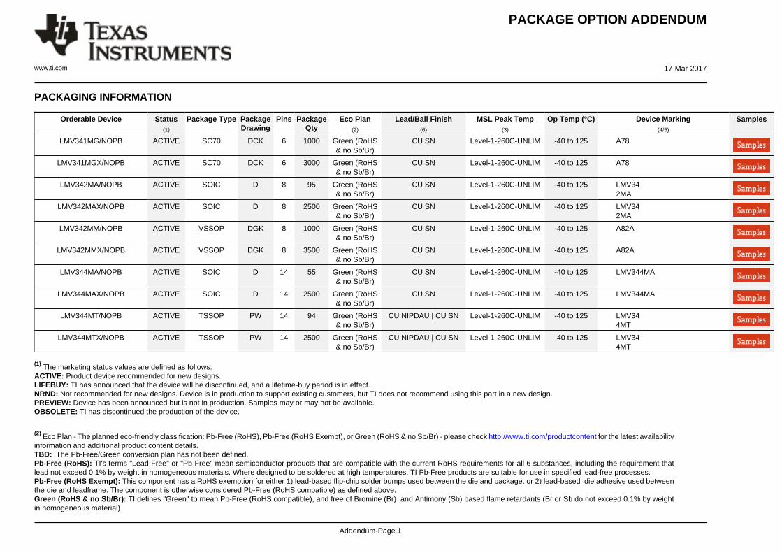
12 Mechanical, Packaging, and Orderable InformationThe following pages include mechanical, packaging, and orderable information. This information is the mostcurrent data available for the designated devices. This data is subject to change without notice and revision ofthis document. For browser-based versions of this data sheet, refer to the left-hand navigation.
PACKAGE OPTION ADDENDUM
www.ti.com 17-Mar-2017
Addendum-Page 1
PACKAGING INFORMATION
Orderable Device Status(1)
Package Type PackageDrawing
Pins PackageQty
Eco Plan(2)
Lead/Ball Finish(6)
MSL Peak Temp(3)
Op Temp (°C) Device Marking(4/5)
Samples
LMV341MG/NOPB ACTIVE SC70 DCK 6 1000 Green (RoHS& no Sb/Br)
CU SN Level-1-260C-UNLIM -40 to 125 A78
LMV341MGX/NOPB ACTIVE SC70 DCK 6 3000 Green (RoHS& no Sb/Br)
CU SN Level-1-260C-UNLIM -40 to 125 A78
LMV342MA/NOPB ACTIVE SOIC D 8 95 Green (RoHS& no Sb/Br)
CU SN Level-1-260C-UNLIM -40 to 125 LMV342MA
LMV342MAX/NOPB ACTIVE SOIC D 8 2500 Green (RoHS& no Sb/Br)
CU SN Level-1-260C-UNLIM -40 to 125 LMV342MA
LMV342MM/NOPB ACTIVE VSSOP DGK 8 1000 Green (RoHS& no Sb/Br)
CU SN Level-1-260C-UNLIM -40 to 125 A82A
LMV342MMX/NOPB ACTIVE VSSOP DGK 8 3500 Green (RoHS& no Sb/Br)
CU SN Level-1-260C-UNLIM -40 to 125 A82A
LMV344MA/NOPB ACTIVE SOIC D 14 55 Green (RoHS& no Sb/Br)
CU SN Level-1-260C-UNLIM -40 to 125 LMV344MA
LMV344MAX/NOPB ACTIVE SOIC D 14 2500 Green (RoHS& no Sb/Br)
CU SN Level-1-260C-UNLIM -40 to 125 LMV344MA
LMV344MT/NOPB ACTIVE TSSOP PW 14 94 Green (RoHS& no Sb/Br)
CU NIPDAU | CU SN Level-1-260C-UNLIM -40 to 125 LMV344MT
LMV344MTX/NOPB ACTIVE TSSOP PW 14 2500 Green (RoHS& no Sb/Br)
CU NIPDAU | CU SN Level-1-260C-UNLIM -40 to 125 LMV344MT
(1) The marketing status values are defined as follows:ACTIVE: Product device recommended for new designs.LIFEBUY: TI has announced that the device will be discontinued, and a lifetime-buy period is in effect.NRND: Not recommended for new designs. Device is in production to support existing customers, but TI does not recommend using this part in a new design.PREVIEW: Device has been announced but is not in production. Samples may or may not be available.OBSOLETE: TI has discontinued the production of the device.
(2) Eco Plan - The planned eco-friendly classification: Pb-Free (RoHS), Pb-Free (RoHS Exempt), or Green (RoHS & no Sb/Br) - please check http://www.ti.com/productcontent for the latest availabilityinformation and additional product content details.TBD: The Pb-Free/Green conversion plan has not been defined.Pb-Free (RoHS): TI's terms "Lead-Free" or "Pb-Free" mean semiconductor products that are compatible with the current RoHS requirements for all 6 substances, including the requirement thatlead not exceed 0.1% by weight in homogeneous materials. Where designed to be soldered at high temperatures, TI Pb-Free products are suitable for use in specified lead-free processes.Pb-Free (RoHS Exempt): This component has a RoHS exemption for either 1) lead-based flip-chip solder bumps used between the die and package, or 2) lead-based die adhesive used betweenthe die and leadframe. The component is otherwise considered Pb-Free (RoHS compatible) as defined above.Green (RoHS & no Sb/Br): TI defines "Green" to mean Pb-Free (RoHS compatible), and free of Bromine (Br) and Antimony (Sb) based flame retardants (Br or Sb do not exceed 0.1% by weightin homogeneous material)
PACKAGE OPTION ADDENDUM
www.ti.com 17-Mar-2017
Addendum-Page 2
(3) MSL, Peak Temp. - The Moisture Sensitivity Level rating according to the JEDEC industry standard classifications, and peak solder temperature.
(4) There may be additional marking, which relates to the logo, the lot trace code information, or the environmental category on the device.
(5) Multiple Device Markings will be inside parentheses. Only one Device Marking contained in parentheses and separated by a "~" will appear on a device. If a line is indented then it is a continuationof the previous line and the two combined represent the entire Device Marking for that device.
(6) Lead/Ball Finish - Orderable Devices may have multiple material finish options. Finish options are separated by a vertical ruled line. Lead/Ball Finish values may wrap to two lines if the finishvalue exceeds the maximum column width.
Important Information and Disclaimer:The information provided on this page represents TI's knowledge and belief as of the date that it is provided. TI bases its knowledge and belief on informationprovided by third parties, and makes no representation or warranty as to the accuracy of such information. Efforts are underway to better integrate information from third parties. TI has taken andcontinues to take reasonable steps to provide representative and accurate information but may not have conducted destructive testing or chemical analysis on incoming materials and chemicals.TI and TI suppliers consider certain information to be proprietary, and thus CAS numbers and other limited information may not be available for release.
In no event shall TI's liability arising out of such information exceed the total purchase price of the TI part(s) at issue in this document sold by TI to Customer on an annual basis.
OTHER QUALIFIED VERSIONS OF LMV341-N, LMV344-N :
• Automotive: LMV341-Q1, LMV344-Q1
NOTE: Qualified Version Definitions:
• Automotive - Q100 devices qualified for high-reliability automotive applications targeting zero defects
TAPE AND REEL INFORMATION
*All dimensions are nominal
Device PackageType
PackageDrawing
Pins SPQ ReelDiameter
(mm)
ReelWidth
W1 (mm)
A0(mm)
B0(mm)
K0(mm)
P1(mm)
W(mm)
Pin1Quadrant
LMV341MG/NOPB SC70 DCK 6 1000 178.0 8.4 2.25 2.45 1.2 4.0 8.0 Q3
LMV341MGX/NOPB SC70 DCK 6 3000 178.0 8.4 2.25 2.45 1.2 4.0 8.0 Q3
LMV342MAX/NOPB SOIC D 8 2500 330.0 12.4 6.5 5.4 2.0 8.0 12.0 Q1
LMV342MM/NOPB VSSOP DGK 8 1000 178.0 12.4 5.3 3.4 1.4 8.0 12.0 Q1
LMV342MMX/NOPB VSSOP DGK 8 3500 330.0 12.4 5.3 3.4 1.4 8.0 12.0 Q1
LMV344MAX/NOPB SOIC D 14 2500 330.0 16.4 6.5 9.35 2.3 8.0 16.0 Q1
LMV344MTX/NOPB TSSOP PW 14 2500 330.0 12.4 6.95 5.6 1.6 8.0 12.0 Q1
LMV344MTX/NOPB TSSOP PW 14 2500 330.0 12.4 6.95 5.6 1.6 8.0 12.0 Q1
PACKAGE MATERIALS INFORMATION
www.ti.com 6-Jun-2018
Pack Materials-Page 1

*All dimensions are nominal
Device Package Type Package Drawing Pins SPQ Length (mm) Width (mm) Height (mm)
LMV341MG/NOPB SC70 DCK 6 1000 210.0 185.0 35.0
LMV341MGX/NOPB SC70 DCK 6 3000 210.0 185.0 35.0
LMV342MAX/NOPB SOIC D 8 2500 367.0 367.0 35.0
LMV342MM/NOPB VSSOP DGK 8 1000 210.0 185.0 35.0
LMV342MMX/NOPB VSSOP DGK 8 3500 367.0 367.0 35.0
LMV344MAX/NOPB SOIC D 14 2500 367.0 367.0 35.0
LMV344MTX/NOPB TSSOP PW 14 2500 367.0 367.0 35.0
LMV344MTX/NOPB TSSOP PW 14 2500 367.0 367.0 35.0
PACKAGE MATERIALS INFORMATION
www.ti.com 6-Jun-2018
Pack Materials-Page 2


IMPORTANT NOTICE
Texas Instruments Incorporated (TI) reserves the right to make corrections, enhancements, improvements and other changes to itssemiconductor products and services per JESD46, latest issue, and to discontinue any product or service per JESD48, latest issue. Buyersshould obtain the latest relevant information before placing orders and should verify that such information is current and complete.TI’s published terms of sale for semiconductor products (http://www.ti.com/sc/docs/stdterms.htm) apply to the sale of packaged integratedcircuit products that TI has qualified and released to market. Additional terms may apply to the use or sale of other types of TI products andservices.Reproduction of significant portions of TI information in TI data sheets is permissible only if reproduction is without alteration and isaccompanied by all associated warranties, conditions, limitations, and notices. TI is not responsible or liable for such reproduceddocumentation. Information of third parties may be subject to additional restrictions. Resale of TI products or services with statementsdifferent from or beyond the parameters stated by TI for that product or service voids all express and any implied warranties for theassociated TI product or service and is an unfair and deceptive business practice. TI is not responsible or liable for any such statements.Buyers and others who are developing systems that incorporate TI products (collectively, “Designers”) understand and agree that Designersremain responsible for using their independent analysis, evaluation and judgment in designing their applications and that Designers havefull and exclusive responsibility to assure the safety of Designers' applications and compliance of their applications (and of all TI productsused in or for Designers’ applications) with all applicable regulations, laws and other applicable requirements. Designer represents that, withrespect to their applications, Designer has all the necessary expertise to create and implement safeguards that (1) anticipate dangerousconsequences of failures, (2) monitor failures and their consequences, and (3) lessen the likelihood of failures that might cause harm andtake appropriate actions. Designer agrees that prior to using or distributing any applications that include TI products, Designer willthoroughly test such applications and the functionality of such TI products as used in such applications.TI’s provision of technical, application or other design advice, quality characterization, reliability data or other services or information,including, but not limited to, reference designs and materials relating to evaluation modules, (collectively, “TI Resources”) are intended toassist designers who are developing applications that incorporate TI products; by downloading, accessing or using TI Resources in anyway, Designer (individually or, if Designer is acting on behalf of a company, Designer’s company) agrees to use any particular TI Resourcesolely for this purpose and subject to the terms of this Notice.TI’s provision of TI Resources does not expand or otherwise alter TI’s applicable published warranties or warranty disclaimers for TIproducts, and no additional obligations or liabilities arise from TI providing such TI Resources. TI reserves the right to make corrections,enhancements, improvements and other changes to its TI Resources. TI has not conducted any testing other than that specificallydescribed in the published documentation for a particular TI Resource.Designer is authorized to use, copy and modify any individual TI Resource only in connection with the development of applications thatinclude the TI product(s) identified in such TI Resource. NO OTHER LICENSE, EXPRESS OR IMPLIED, BY ESTOPPEL OR OTHERWISETO ANY OTHER TI INTELLECTUAL PROPERTY RIGHT, AND NO LICENSE TO ANY TECHNOLOGY OR INTELLECTUAL PROPERTYRIGHT OF TI OR ANY THIRD PARTY IS GRANTED HEREIN, including but not limited to any patent right, copyright, mask work right, orother intellectual property right relating to any combination, machine, or process in which TI products or services are used. Informationregarding or referencing third-party products or services does not constitute a license to use such products or services, or a warranty orendorsement thereof. Use of TI Resources may require a license from a third party under the patents or other intellectual property of thethird party, or a license from TI under the patents or other intellectual property of TI.TI RESOURCES ARE PROVIDED “AS IS” AND WITH ALL FAULTS. TI DISCLAIMS ALL OTHER WARRANTIES ORREPRESENTATIONS, EXPRESS OR IMPLIED, REGARDING RESOURCES OR USE THEREOF, INCLUDING BUT NOT LIMITED TOACCURACY OR COMPLETENESS, TITLE, ANY EPIDEMIC FAILURE WARRANTY AND ANY IMPLIED WARRANTIES OFMERCHANTABILITY, FITNESS FOR A PARTICULAR PURPOSE, AND NON-INFRINGEMENT OF ANY THIRD PARTY INTELLECTUALPROPERTY RIGHTS. TI SHALL NOT BE LIABLE FOR AND SHALL NOT DEFEND OR INDEMNIFY DESIGNER AGAINST ANY CLAIM,INCLUDING BUT NOT LIMITED TO ANY INFRINGEMENT CLAIM THAT RELATES TO OR IS BASED ON ANY COMBINATION OFPRODUCTS EVEN IF DESCRIBED IN TI RESOURCES OR OTHERWISE. IN NO EVENT SHALL TI BE LIABLE FOR ANY ACTUAL,DIRECT, SPECIAL, COLLATERAL, INDIRECT, PUNITIVE, INCIDENTAL, CONSEQUENTIAL OR EXEMPLARY DAMAGES INCONNECTION WITH OR ARISING OUT OF TI RESOURCES OR USE THEREOF, AND REGARDLESS OF WHETHER TI HAS BEENADVISED OF THE POSSIBILITY OF SUCH DAMAGES.Unless TI has explicitly designated an individual product as meeting the requirements of a particular industry standard (e.g., ISO/TS 16949and ISO 26262), TI is not responsible for any failure to meet such industry standard requirements.Where TI specifically promotes products as facilitating functional safety or as compliant with industry functional safety standards, suchproducts are intended to help enable customers to design and create their own applications that meet applicable functional safety standardsand requirements. Using products in an application does not by itself establish any safety features in the application. Designers mustensure compliance with safety-related requirements and standards applicable to their applications. Designer may not use any TI products inlife-critical medical equipment unless authorized officers of the parties have executed a special contract specifically governing such use.Life-critical medical equipment is medical equipment where failure of such equipment would cause serious bodily injury or death (e.g., lifesupport, pacemakers, defibrillators, heart pumps, neurostimulators, and implantables). Such equipment includes, without limitation, allmedical devices identified by the U.S. Food and Drug Administration as Class III devices and equivalent classifications outside the U.S.TI may expressly designate certain products as completing a particular qualification (e.g., Q100, Military Grade, or Enhanced Product).Designers agree that it has the necessary expertise to select the product with the appropriate qualification designation for their applicationsand that proper product selection is at Designers’ own risk. Designers are solely responsible for compliance with all legal and regulatoryrequirements in connection with such selection.Designer will fully indemnify TI and its representatives against any damages, costs, losses, and/or liabilities arising out of Designer’s non-compliance with the terms and provisions of this Notice.
Mailing Address: Texas Instruments, Post Office Box 655303, Dallas, Texas 75265Copyright © 2018, Texas Instruments Incorporated


![CARB Document: ......CERT STD SFTP @ 4000 miles SFTP @ * miles CO [g/mi] com osite CERT STD CO sc03 CERT 0.09 STD 0.14 CERT 1.7 STD 8.0 CERT 0.04 STD 0.20 CERT 2.4 STD 2.7 CERT STD](https://img.pdfslide.net/doc/110x75/601fc6dcad09a45b411bb1e3/carb-document-cert-std-sftp-4000-miles-sftp-miles-co-gmi-com-osite.jpg)