Embed Size (px)
Citation preview
LMX2615EVM-CVAL Wideband 15-GHzSynthesizer
User's Guide
Literature Number: SNAU218November 2018
2 SNAU218–November 2018Submit Documentation Feedback
Copyright © 2018, Texas Instruments Incorporated
Table of Contents
Contents
1 Evaluation Board Setup and Description ................................................................................ 42 Setting Up the Software ........................................................................................................ 53 Bringing LMX2615 to a Lock State ......................................................................................... 64 Current Loop Filter Configuration .......................................................................................... 75 Typical Phase Noise ............................................................................................................. 8Appendix A Schematic ................................................................................................................ 10Appendix B Bill of Materials......................................................................................................... 11Appendix C PCB Board Specifications.......................................................................................... 13Appendix D Proper Jumper and Switch Positions .......................................................................... 18
3SNAU218–November 2018Submit Documentation Feedback
Copyright © 2018, Texas Instruments Incorporated
LMX2615EVM-CVAL Wideband 15-GHz Synthesizer
User's GuideSNAU218–November 2018
LMX2615EVM-CVAL Wideband 15-GHz Synthesizer
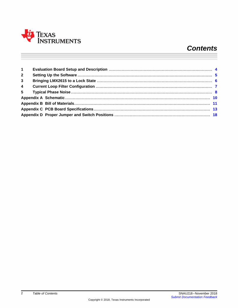
Figure 1. LMX2615EVM-CVAL
+3.3 V
To Spectrum
Analyzer
50
:
Te
rmin
ati
on
100 MHz Input
Reference
Lock Detect
LED
Readback/
Lock Detect
Selector
Switch
Reference Pro
SPI interface
FS Switches
Power
Jumpers
Evaluation Board Setup and Description www.ti.com
4 SNAU218–November 2018Submit Documentation Feedback
Copyright © 2018, Texas Instruments Incorporated
LMX2615EVM-CVAL Wideband 15-GHz Synthesizer
1 Evaluation Board Setup and Description
SPACER
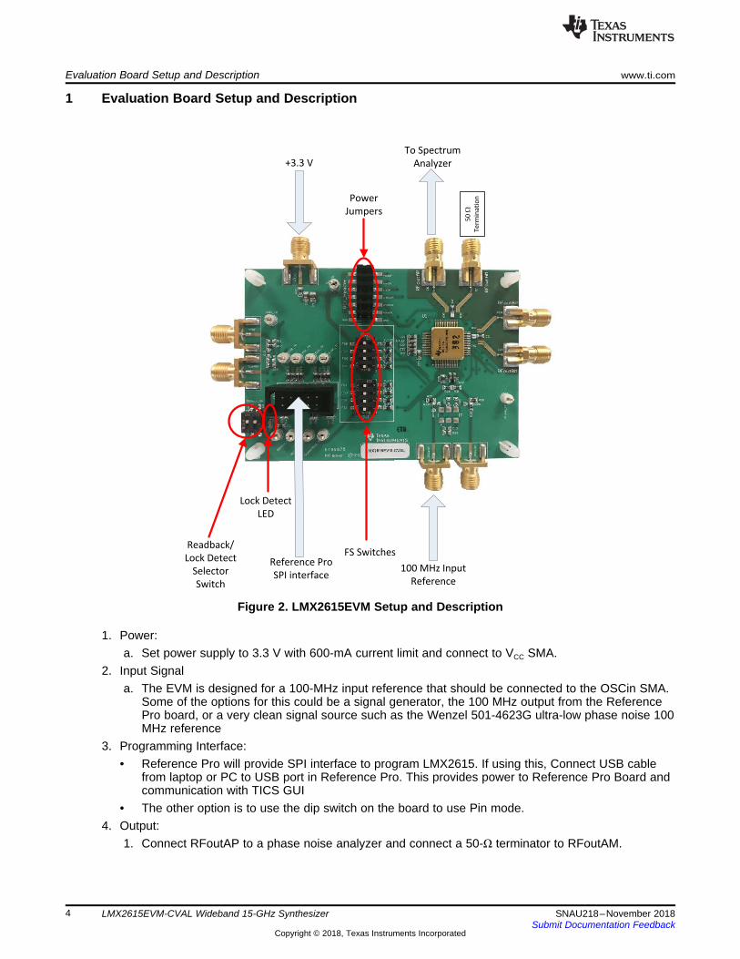
Figure 2. LMX2615EVM Setup and Description
1. Power:a. Set power supply to 3.3 V with 600-mA current limit and connect to VCC SMA.
2. Input Signala. The EVM is designed for a 100-MHz input reference that should be connected to the OSCin SMA.
Some of the options for this could be a signal generator, the 100 MHz output from the ReferencePro board, or a very clean signal source such as the Wenzel 501-4623G ultra-low phase noise 100MHz reference
3. Programming Interface:• Reference Pro will provide SPI interface to program LMX2615. If using this, Connect USB cable
from laptop or PC to USB port in Reference Pro. This provides power to Reference Pro Board andcommunication with TICS GUI
• The other option is to use the dip switch on the board to use Pin mode.4. Output:
1. Connect RFoutAP to a phase noise analyzer and connect a 50-Ω terminator to RFoutAM.
www.ti.com Setting Up the Software
5SNAU218–November 2018Submit Documentation Feedback
Copyright © 2018, Texas Instruments Incorporated
LMX2615EVM-CVAL Wideband 15-GHz Synthesizer
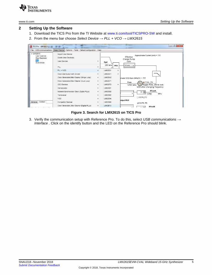
2 Setting Up the Software1. Download the TICS Pro from the TI Website at www.ti.com/tool/TICSPRO-SW and install.2. From the menu bar choose Select Device → PLL + VCO → LMX2615
Figure 3. Search for LMX2615 on TICS Pro
3. Verify the communication setup with Reference Pro. To do this, select USB communications →Interface . Click on the identify button and the LED on the Reference Pro should blink.
Bringing LMX2615 to a Lock State www.ti.com
6 SNAU218–November 2018Submit Documentation Feedback
Copyright © 2018, Texas Instruments Incorporated
LMX2615EVM-CVAL Wideband 15-GHz Synthesizer
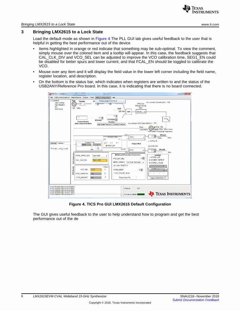
3 Bringing LMX2615 to a Lock StateLoad the default mode as shown in Figure 4 The PLL GUI tab gives useful feedback to the user that ishelpful in getting the best performance out of the device• Items highlighted in orange or red indicate that something may be sub-optimal. To view the comment,
simply mouse over the colored item and a tooltip will appear. In this case, the feedback suggests thatCAL_CLK_DIV and VCO_SEL can be adjusted to improve the VCO calibration time, SEG1_EN couldbe disabled for better spurs and lower current, and that FCAL_EN should be toggled to calibrate theVCO.
• Mouse over any item and it will display the field value in the lower left corner including the field name,register location, and description.
• On the bottom is the status bar, which indicates when registers are written to and the status of theUSB2ANY/Reference Pro board. In this case, it is indicating that there is no board connected.
Figure 4. TICS Pro GUI LMX2615 Default Configuration
The GUI gives useful feedback to the user to help understand how to program and get the bestperformance out of the de
www.ti.com Current Loop Filter Configuration
7SNAU218–November 2018Submit Documentation Feedback
Copyright © 2018, Texas Instruments Incorporated
LMX2615EVM-CVAL Wideband 15-GHz Synthesizer
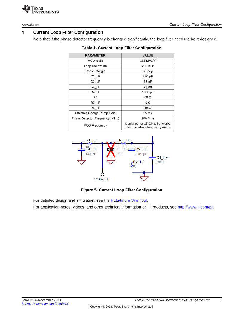
4 Current Loop Filter ConfigurationNote that if the phase detector frequency is changed significantly, the loop filter needs to be redesigned.
Table 1. Current Loop Filter Configuration
PARAMETER VALUEVCO Gain 132 MHz/V
Loop Bandwidth 285 kHzPhase Margin 65 deg
C1_LF 390 pFC2_LF 68 nFC3_LF OpenC4_LF 1800 pF
R2 68 Ω
R3_LF 0 Ω
R4_LF 18 Ω
Effective Charge Pump Gain 15 mAPhase Detector Frequency (MHz) 200 MHz
VCO Frequency Designed for 15 GHz, but worksover the whole frequency range
Figure 5. Current Loop Filter Configuration
For detailed design and simulation, see the PLLatinum Sim Tool.
For application notes, videos, and other technical information on TI products, see http://www.ti.com/pll.
Typical Phase Noise www.ti.com
8 SNAU218–November 2018Submit Documentation Feedback
Copyright © 2018, Texas Instruments Incorporated
LMX2615EVM-CVAL Wideband 15-GHz Synthesizer
5 Typical Phase Noise
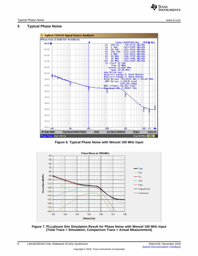
Figure 6. Typical Phase Noise with Wenzel 100 MHz Input
Figure 7. PLLatinum Sim Simulation Result for Phase Noise with Wenzel 100 MHz Input(Total Trace = Simulation, Comparison Trace = Actual Measurement)
www.ti.com Typical Phase Noise
9SNAU218–November 2018Submit Documentation Feedback
Copyright © 2018, Texas Instruments Incorporated
LMX2615EVM-CVAL Wideband 15-GHz Synthesizer
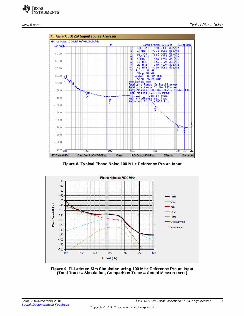
Figure 8. Typical Phase Noise 100 MHz Reference Pro as Input
Figure 9. PLLatinum Sim Simulation using 100 MHz Reference Pro as Input(Total Trace = Simulation, Comparison Trace = Actual Measurement)
10 SNAU218–November 2018Submit Documentation Feedback
Copyright © 2018, Texas Instruments Incorporated
Schematic
Appendix ASNAU218–November 2018
Schematic
Figure 10. Schematic
11SNAU218–November 2018Submit Documentation Feedback
Copyright © 2018, Texas Instruments Incorporated
Bill of Materials
Appendix BSNAU218–November 2018
Bill of Materials
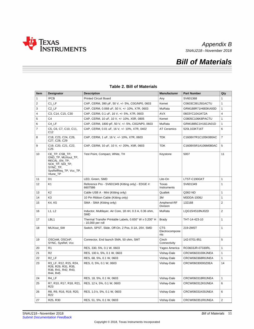
Table 2. Bill of MaterialsItem Designator Description Manufacturer Part Number Qty
1 !PCB Printed Circuit Board Any SV601368 1
2 C1_LF CAP, CERM, 390 pF, 50 V, +/- 5%, C0G/NP0, 0603 Kemet C0603C391J5GACTU 1
3 C2_LF CAP, CERM, 0.068 uF, 50 V, +/- 10%, X7R, 0603 MuRata GRM188R71H683KA93D 1
4 C3, C14, C15, C30 CAP, CERM, 0.1 uF, 16 V, +/- 5%, X7R, 0603 AVX 0603YC104JAT2A 4
5 C4 CAP, CERM, 10 uF, 10 V, +/- 10%, X5R, 0805 Kemet C0805C106K8PACTU 1
6 C4_LF CAP, CERM, 1800 pF, 50 V, +/- 5%, C0G/NP0, 0603 MuRata GRM1885C1H182JA01D 1
7 C5, C6, C7, C10, C11,C12
CAP, CERM, 0.01 uF, 16 V, +/- 10%, X7R, 0402 AT Ceramics 520L103KT16T 6
8 C18, C23, C24, C26,C27, C28, C29
CAP, CERM, 1 uF, 16 V, +/- 10%, X7R, 0603 TDK C1608X7R1C105K080AC 7
9 C19, C20, C21, C22,C25
CAP, CERM, 10 uF, 10 V, +/- 20%, X5R, 0603 TDK C1608X5R1A106M080AC 5
10 CE_TP, CSB_TP,GND_TP, MUXout_TP,RECAL_EN_TP,SCK_TP, SDI_TP,SYNC_TP,SysRefReq_TP, Vcc_TP,Vtune_TP
Test Point, Compact, White, TH Keystone 5007 11
11 D1 LED, Green, SMD Lite-On LTST-C190GKT 1
12 K1 Reference Pro - SV601349 (Kitting only) - EDGE #:6607586
TexasInstruments
SV601349 1
13 K2 Cable USB A - Mini (Kitting only) Qualtek Q362-ND 1
14 K3 10 Pin Ribbon Cable (Kitting only) 3M M3DDA-1006J 1
15 K4, K5 SMA - SMA (Kitting only) Amphenol-RFDivision
132168 2
16 L1, L2 Inductor, Multilayer, Air Core, 18 nH, 0.3 A, 0.36 ohm,SMD
MuRata LQG15HS18NJ02D 2
17 LBL1 Thermal Transfer Printable Labels, 0.650" W x 0.200" H- 10,000 per roll
Brady THT-14-423-10 1
18 MUXout_SW Switch, SPST, Slide, Off-On, 2 Pos, 0.1A, 20V, SMD CTSElectrocomponents
219-2MST 1
19 OSCinM, OSCinP,SYNC, SysRef, Vcc
Connector, End launch SMA, 50 ohm, SMT CinchConnectivity
142-0701-851 5
20 R1 RES, 330, 5%, 0.1 W, 0603 Yageo America RC0603JR-07330RL 1
21 R2 RES, 100 k, 5%, 0.1 W, 0603 Vishay-Dale CRCW0603100KJNEA 1
22 R2_LF RES, 68, 5%, 0.1 W, 0603 Vishay-Dale CRCW060368R0JNEA 1
23 R3_LF, R12, R15, R24,R26, R29, R31, R35,R36, R41, R42, R43,R44, R45
RES, 0, 5%, 0.1 W, 0603 Vishay-Dale CRCW06030000Z0EA 14
24 R4_LF RES, 18, 5%, 0.1 W, 0603 Vishay-Dale CRCW060318R0JNEA 1
25 R7, R10, R17, R18, R21,R23
RES, 12 k, 5%, 0.1 W, 0603 Vishay-Dale CRCW060312K0JNEA 6
26 R8, R9, R16, R19, R20,R22
RES, 1.0 k, 5%, 0.1 W, 0603 Vishay-Dale CRCW06031K00JNEA 6
27 R25, R30 RES, 51, 5%, 0.1 W, 0603 Vishay-Dale CRCW060351R0JNEA 2
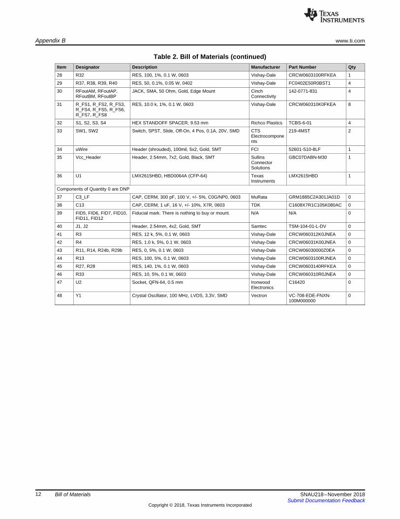
Appendix B www.ti.com
12 SNAU218–November 2018Submit Documentation Feedback
Copyright © 2018, Texas Instruments Incorporated
Bill of Materials
Table 2. Bill of Materials (continued)Item Designator Description Manufacturer Part Number Qty
28 R32 RES, 100, 1%, 0.1 W, 0603 Vishay-Dale CRCW0603100RFKEA 1
29 R37, R38, R39, R40 RES, 50, 0.1%, 0.05 W, 0402 Vishay-Dale FC0402E50R0BST1 4
30 RFoutAM, RFoutAP,RFoutBM, RFoutBP
JACK, SMA, 50 Ohm, Gold, Edge Mount CinchConnectivity
142-0771-831 4
31 R_FS1, R_FS2, R_FS3,R_FS4, R_FS5, R_FS6,R_FS7, R_FS8
RES, 10.0 k, 1%, 0.1 W, 0603 Vishay-Dale CRCW060310K0FKEA 8
32 S1, S2, S3, S4 HEX STANDOFF SPACER, 9.53 mm Richco Plastics TCBS-6-01 4
33 SW1, SW2 Switch, SPST, Slide, Off-On, 4 Pos, 0.1A, 20V, SMD CTSElectrocomponents
219-4MST 2
34 uWire Header (shrouded), 100mil, 5x2, Gold, SMT FCI 52601-S10-8LF 1
35 Vcc_Header Header, 2.54mm, 7x2, Gold, Black, SMT SullinsConnectorSolutions
GBC07DABN-M30 1
36 U1 LMX2615HBD, HBD0064A (CFP-64) TexasInstruments
LMX2615HBD 1
Components of Quantity 0 are DNP
37 C3_LF CAP, CERM, 300 pF, 100 V, +/- 5%, C0G/NP0, 0603 MuRata GRM1885C2A301JA01D 0
38 C13 CAP, CERM, 1 uF, 16 V, +/- 10%, X7R, 0603 TDK C1608X7R1C105K080AC 0
39 FID5, FID6, FID7, FID10,FID11, FID12
Fiducial mark. There is nothing to buy or mount. N/A N/A 0
40 J1, J2 Header, 2.54mm, 4x2, Gold, SMT Samtec TSM-104-01-L-DV 0
41 R3 RES, 12 k, 5%, 0.1 W, 0603 Vishay-Dale CRCW060312K0JNEA 0
42 R4 RES, 1.0 k, 5%, 0.1 W, 0603 Vishay-Dale CRCW06031K00JNEA 0
43 R11, R14, R24b, R29b RES, 0, 5%, 0.1 W, 0603 Vishay-Dale CRCW06030000Z0EA 0
44 R13 RES, 100, 5%, 0.1 W, 0603 Vishay-Dale CRCW0603100RJNEA 0
45 R27, R28 RES, 140, 1%, 0.1 W, 0603 Vishay-Dale CRCW0603140RFKEA 0
46 R33 RES, 10, 5%, 0.1 W, 0603 Vishay-Dale CRCW060310R0JNEA 0
47 U2 Socket, QFN-64, 0.5 mm IronwoodElectronics
C16420 0
48 Y1 Crystal Oscillator, 100 MHz, LVDS, 3.3V, SMD Vectron VC-708-EDE-FNXN-100M000000
0
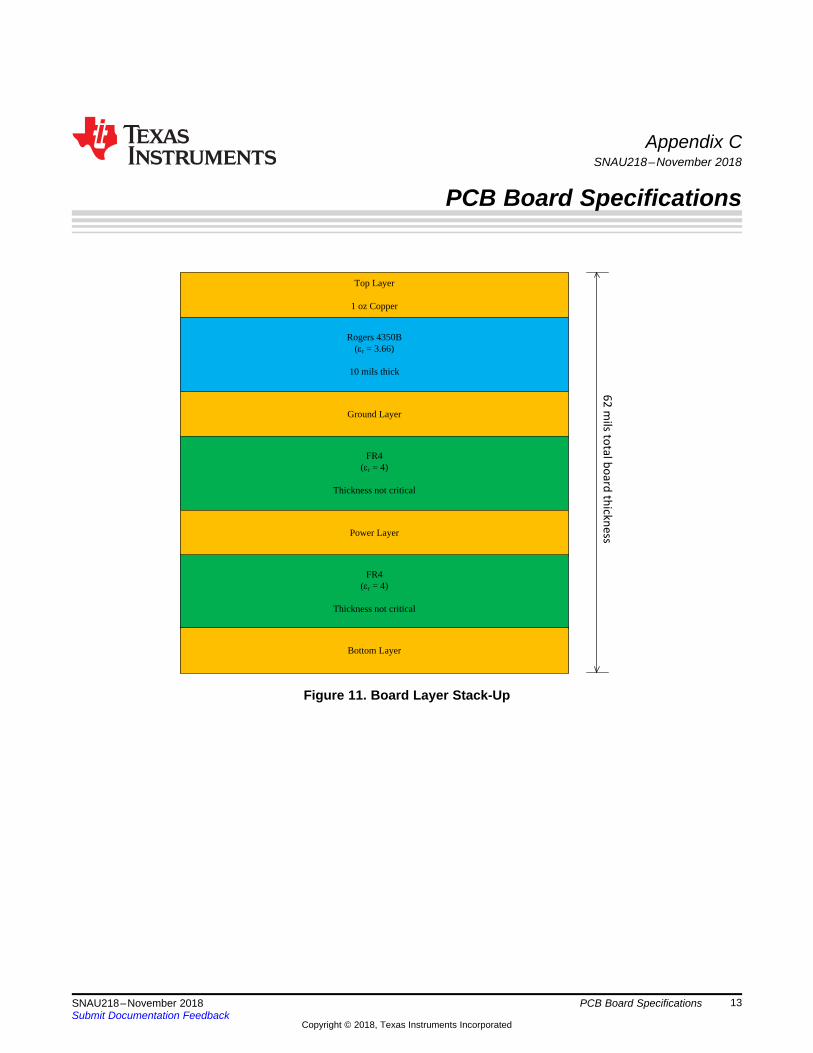
Top Layer
1 oz Copper
Rogers 4350B(Hr = 3.66)
10 mils thick
Ground Layer
FR4(Hr = 4)
Thickness not critical
Power Layer
FR4(Hr = 4)
Thickness not critical
Bottom Layer
62
mils
tota
l bo
ard
thic
kn
ess
13SNAU218–November 2018Submit Documentation Feedback
Copyright © 2018, Texas Instruments Incorporated
PCB Board Specifications
Appendix CSNAU218–November 2018
PCB Board Specifications
Figure 11. Board Layer Stack-Up
Appendix C www.ti.com
14 SNAU218–November 2018Submit Documentation Feedback
Copyright © 2018, Texas Instruments Incorporated
PCB Board Specifications
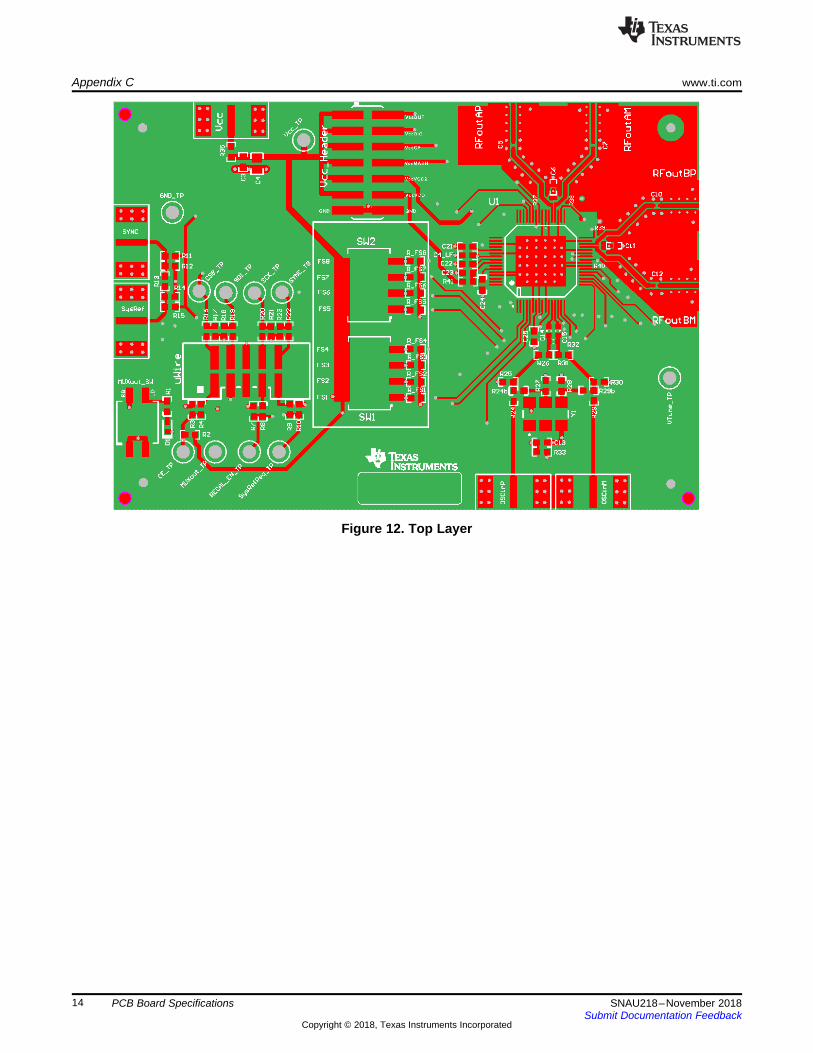
Figure 12. Top Layer
www.ti.com Appendix C
15SNAU218–November 2018Submit Documentation Feedback
Copyright © 2018, Texas Instruments Incorporated
PCB Board Specifications
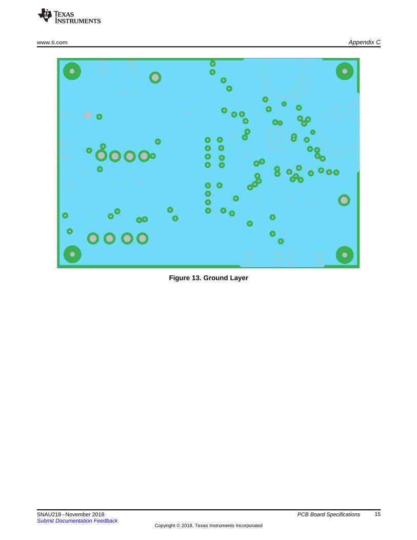
Figure 13. Ground Layer
Appendix C www.ti.com
16 SNAU218–November 2018Submit Documentation Feedback
Copyright © 2018, Texas Instruments Incorporated
PCB Board Specifications
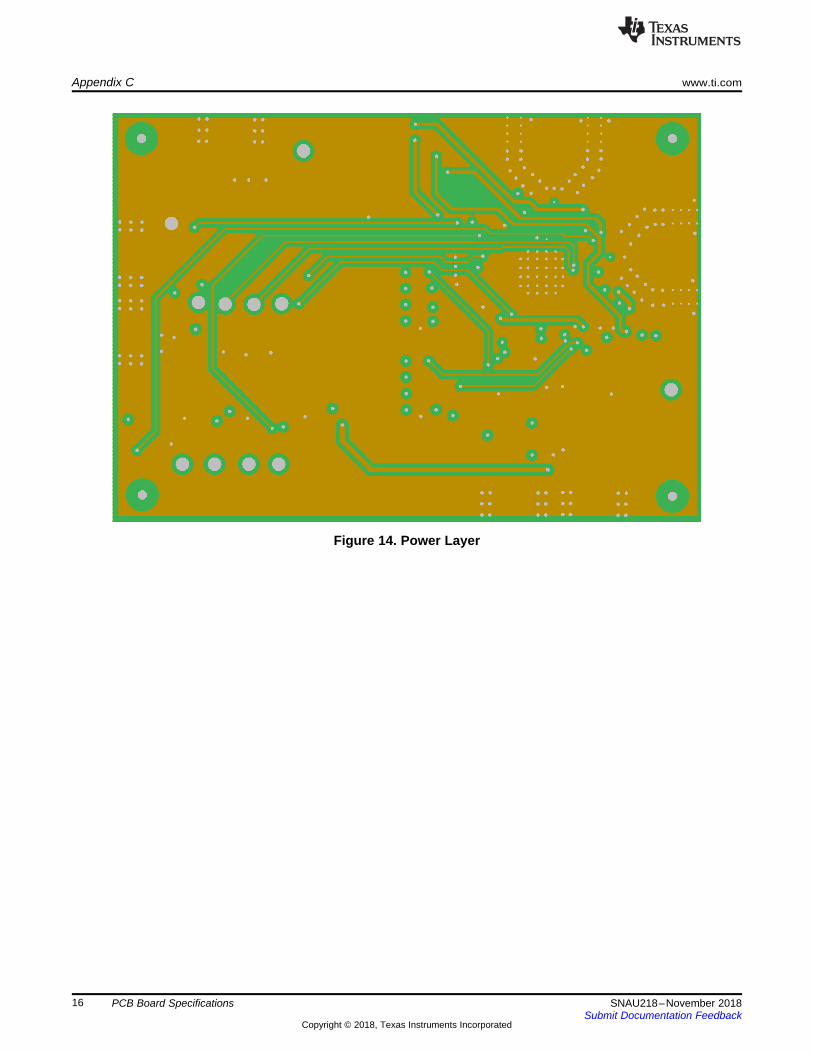
Figure 14. Power Layer
www.ti.com Appendix C
17SNAU218–November 2018Submit Documentation Feedback
Copyright © 2018, Texas Instruments Incorporated
PCB Board Specifications
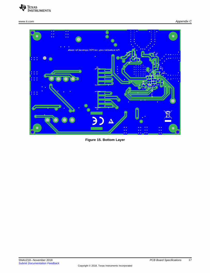
Figure 15. Bottom Layer
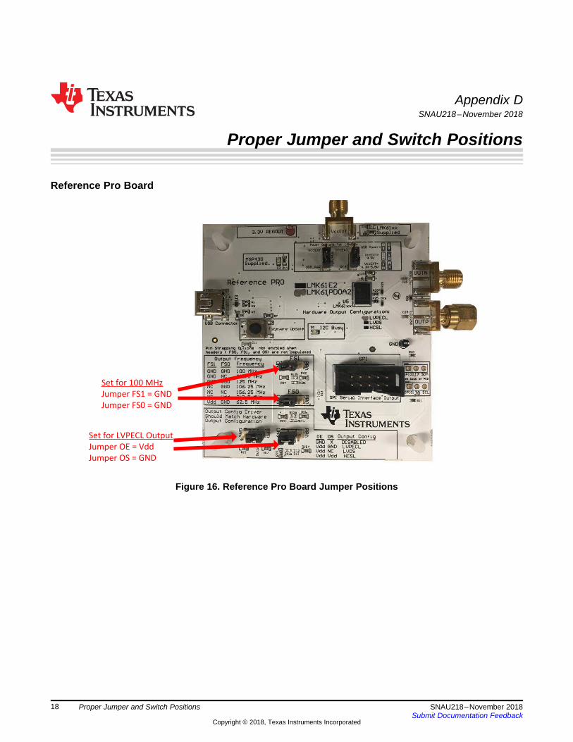
Set for 100 MHz
Jumper FS1 = GND
Jumper FS0 = GND
Set for LVPECL Output
Jumper OE = Vdd
Jumper OS = GND
18 SNAU218–November 2018Submit Documentation Feedback
Copyright © 2018, Texas Instruments Incorporated
Proper Jumper and Switch Positions
Appendix DSNAU218–November 2018
Proper Jumper and Switch Positions
Reference Pro Board
Figure 16. Reference Pro Board Jumper Positions
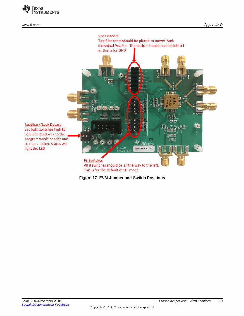
Readback/Lock Detect
Set both switches high to
connect Readback to the
programmable header and
so that a locked status will
light the LED
Vcc Headers
Top 6 headers should be placed to power each
individual Vcc Pin. The bottom header can be left off
as this is for GND
FS Switches
All 8 switches should be all the way to the left.
This is for the default of SPI mode
www.ti.com Appendix D
19SNAU218–November 2018Submit Documentation Feedback
Copyright © 2018, Texas Instruments Incorporated
Proper Jumper and Switch Positions
Figure 17. EVM Jumper and Switch Positions
IMPORTANT NOTICE AND DISCLAIMER
TI PROVIDES TECHNICAL AND RELIABILITY DATA (INCLUDING DATASHEETS), DESIGN RESOURCES (INCLUDING REFERENCEDESIGNS), APPLICATION OR OTHER DESIGN ADVICE, WEB TOOLS, SAFETY INFORMATION, AND OTHER RESOURCES “AS IS”AND WITH ALL FAULTS, AND DISCLAIMS ALL WARRANTIES, EXPRESS AND IMPLIED, INCLUDING WITHOUT LIMITATION ANYIMPLIED WARRANTIES OF MERCHANTABILITY, FITNESS FOR A PARTICULAR PURPOSE OR NON-INFRINGEMENT OF THIRDPARTY INTELLECTUAL PROPERTY RIGHTS.These resources are intended for skilled developers designing with TI products. You are solely responsible for (1) selecting the appropriateTI products for your application, (2) designing, validating and testing your application, and (3) ensuring your application meets applicablestandards, and any other safety, security, or other requirements. These resources are subject to change without notice. TI grants youpermission to use these resources only for development of an application that uses the TI products described in the resource. Otherreproduction and display of these resources is prohibited. No license is granted to any other TI intellectual property right or to any thirdparty intellectual property right. TI disclaims responsibility for, and you will fully indemnify TI and its representatives against, any claims,damages, costs, losses, and liabilities arising out of your use of these resources.TI’s products are provided subject to TI’s Terms of Sale (www.ti.com/legal/termsofsale.html) or other applicable terms available either onti.com or provided in conjunction with such TI products. TI’s provision of these resources does not expand or otherwise alter TI’s applicablewarranties or warranty disclaimers for TI products.
Mailing Address: Texas Instruments, Post Office Box 655303, Dallas, Texas 75265Copyright © 2018, Texas Instruments Incorporated