Embed Size (px)
Citation preview
IN+
IN−OUT
Product
Folder
Sample &Buy
Technical
Documents
Tools &
Software
Support &Community
LM139, LM239, LM339, LM139ALM239A, LM339A, LM2901, LM2901AV, LM2901V
SLCS006T –OCTOBER 1979–REVISED JUNE 2015
LMx39x, LM2901xx Quad Differential Comparators1 Features 3 Description
The LMx39x and the LM2901xx devices consist of1• Wide Supply Ranges
four independent voltage comparators that are– Single Supply: 2 V to 36 V designed to operate from a single power supply over(Tested to 30 V for Non-V Devices and a wide range of voltages. Operation from dual32 V for V-Suffix Devices) supplies also is possible, as long as the difference
between the two supplies is 2 V to 36 V, and VCC is– Dual Supplies: ±1 V to ±18 Vat least 1.5 V more positive than the input common-(Tested to ±15 V for Non-V Devices andmode voltage. Current drain is independent of the±16 V for V-Suffix Devices)supply voltage. The outputs can be connected to• Low Supply-Current Drain Independent of other open-collector outputs to achieve wired-AND
Supply Voltage: 0.8 mA (Typical) relationships.• Low Input Bias Current: 25 nA (Typical)
The LM139 and LM139A devices are characterized• Low Input Offset Current: 3 nA (Typical) (LM139) for operation over the full military temperature range• Low Input Offset Voltage: 2 mV (Typical) of –55°C to 125°C. The LM239 and LM239A devices
are characterized for operation from –25°C to 125°C.• Common-Mode Input Voltage RangeThe LM339 and LM339A devices are characterizedIncludes Groundfor operation from 0°C to 70°C. The LM2901,
• Differential Input Voltage Range Equal to LM2901AV, and LM2901V devices are characterizedMaximum-Rated Supply Voltage: ±36 V for operation from –40°C to 125°C.
• Low Output Saturation VoltageDevice Information(1)
• Output Compatible With TTL, MOS, and CMOSPART NUMBER PACKAGE BODY SIZE (NOM)• On Products Compliant to MIL-PRF-38535,
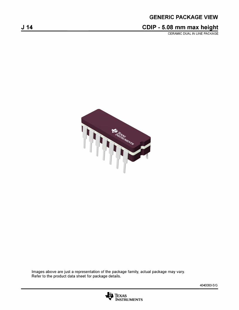
CDIP (14) 21.30 mm × 7.60 mmAll Parameters Are Tested Unless OtherwiseLM139x LCCC (20) 8.90 mm × 8.90 mmNoted. On All Other Products, Production
CFP (14) 9.20 mm × 6.29 mmProcessing Does Not Necessarily Include Testingof All Parameters. LM139x,
LM239x, SOIC (14) 8.70 mm × 3.90 mmLM339x,2 Applications LM2901x• Industrial LM239, LM339x, PDIP (14) 19.30 mm × 6.40 mmLM2901• Automotive
LM239, LM2901 TSSOP (14) 5.00 mm × 4.40 mm– HEV/EV and Power TrainsLM339x, LM2901 SO (14) 10.20 mm × 5.30 mm
– Infotainment and ClustersLM339x SSOP (14) 6.50 mm × 5.30 mm
– Body Control Modules(1) For all available packages, see the orderable addendum at
• Power Supervision the end of the data sheet.• Oscillators• Peak Detectors• Logic Voltage Translation
Simplified Schematic
1
An IMPORTANT NOTICE at the end of this data sheet addresses availability, warranty, changes, use in safety-critical applications,intellectual property matters and other important disclaimers. PRODUCTION DATA.
On products compliant to MIL-PRF-38535, all parameters aretested unless otherwise noted. On all other products, productionprocessing does not necessarily include testing of all parameters.
LM139, LM239, LM339, LM139ALM239A, LM339A, LM2901, LM2901AV, LM2901VSLCS006T –OCTOBER 1979–REVISED JUNE 2015 www.ti.com
Table of Contents1 Features .................................................................. 1 8 Detailed Description ............................................ 10
8.1 Overview ................................................................. 102 Applications ........................................................... 18.2 Functional Block Diagram ....................................... 103 Description ............................................................. 18.3 Feature Description................................................. 104 Revision History..................................................... 28.4 Device Functional Modes........................................ 105 Device Comparison Table ..................................... 3
9 Application and Implementation ........................ 116 Pin Configuration and Functions ......................... 49.1 Application Information............................................ 117 Specifications......................................................... 59.2 Typical Application ................................................. 117.1 Absolute Maximum Ratings ..................................... 5
10 Power Supply Recommendations ..................... 137.2 ESD Ratings.............................................................. 511 Layout................................................................... 137.3 Recommended Operating Conditions....................... 5
11.1 Layout Guidelines ................................................. 137.4 Thermal Information (14-Pin Packages) ................... 511.2 Layout Example .................................................... 137.5 Thermal Information (20-Pin Packages) ................... 5
12 Device and Documentation Support ................. 147.6 Electrical Characteristics for LM139 and LM139A.... 612.1 Related Links ........................................................ 147.7 Electrical Characteristics for LMx39 and LMx39A .... 612.2 Community Resources.......................................... 147.8 Electrical Characteristics for LM2901 ....................... 712.3 Trademarks ........................................................... 147.9 Switching Characteristics for LM2901....................... 812.4 Electrostatic Discharge Caution............................ 147.10 Switching Characteristics for LM139 and LM139A . 812.5 Glossary ................................................................ 147.11 Switching Characteristics for LMx39 and LMx39A . 8
13 Mechanical, Packaging, and Orderable7.12 Typical Characteristics ............................................ 9Information ........................................................... 14
4 Revision HistoryNOTE: Page numbers for previous revisions may differ from page numbers in the current version.
Changes from Revision S (August 2012) to Revision T Page
• Deleted Ordering Information table. ...................................................................................................................................... 1• Added Military Disclaimer to Features list. ............................................................................................................................. 1• Added Applications, Device Information table, Pin Configuration and Functions section, ESD Ratings table, Thermal
Information table, Feature Description section, Device Functional Modes, Application and Implementation section,Power Supply Recommendations section, Layout section, Device and Documentation Support section, andMechanical, Packaging, and Orderable Information section. No specification changes........................................................ 1
2 Submit Documentation Feedback Copyright © 1979–2015, Texas Instruments Incorporated
Product Folder Links: LM139 LM239 LM339 LM139A LM239A LM339A LM2901 LM2901AV LM2901V
LM139, LM239, LM339, LM139ALM239A, LM339A, LM2901, LM2901AV, LM2901V
www.ti.com SLCS006T –OCTOBER 1979–REVISED JUNE 2015
5 Device Comparison Table
PART NUMBER PACKAGE BODY SIZE (NOM)LM139J, LM139AJ CDIP (14) 21.30 mm × 7.60 mmLM139FK, LM139AFK LCCC (20) 8.90 mm × 8.90 mmLM139W, LM139AW CFP (14) 9.20 mm × 6.29 mmLM139D, LM139AD, LM239D, LM293AD, LM339D, SOIC (14) 8.70 mm × 3.90 mmLM339AD, LM2901DLM239N, LM339N, LM339AN, LM2901N PDIP (14) 19.30 mm × 6.40 mmLM239PW, LM2901PW TSSOP (14) 5.00 mm × 4.40 mmLM339NS, LM339ANS, LM2901NS SOP (14) 10.20 mm × 5.30 mmLM339DB, LM339ADB SSOP (14) 6.50 mm × 5.30 mm
Copyright © 1979–2015, Texas Instruments Incorporated Submit Documentation Feedback 3
Product Folder Links: LM139 LM239 LM339 LM139A LM239A LM339A LM2901 LM2901AV LM2901V
3 2 1 20 19
9 10 11 12 13
4
5
6
7
8
18
17
16
15
14
GND
NC
4IN+
NC
4IN−
VCC
NC
2IN−
NC
2IN+
2O
UT
1O
UT
NC
3IN
−
3IN
+
3O
UT
4O
UT
1IN
−
1IN
+
NC
1
2
3
4
5
6
7
14
13
12
11
10
9
8
1OUT
2OUT
VCC
2IN−
2IN+
1IN−
1IN+
OUT3
OUT4
GND
4IN+
4IN−
3IN+
3IN−
LM139, LM239, LM339, LM139ALM239A, LM339A, LM2901, LM2901AV, LM2901VSLCS006T –OCTOBER 1979–REVISED JUNE 2015 www.ti.com
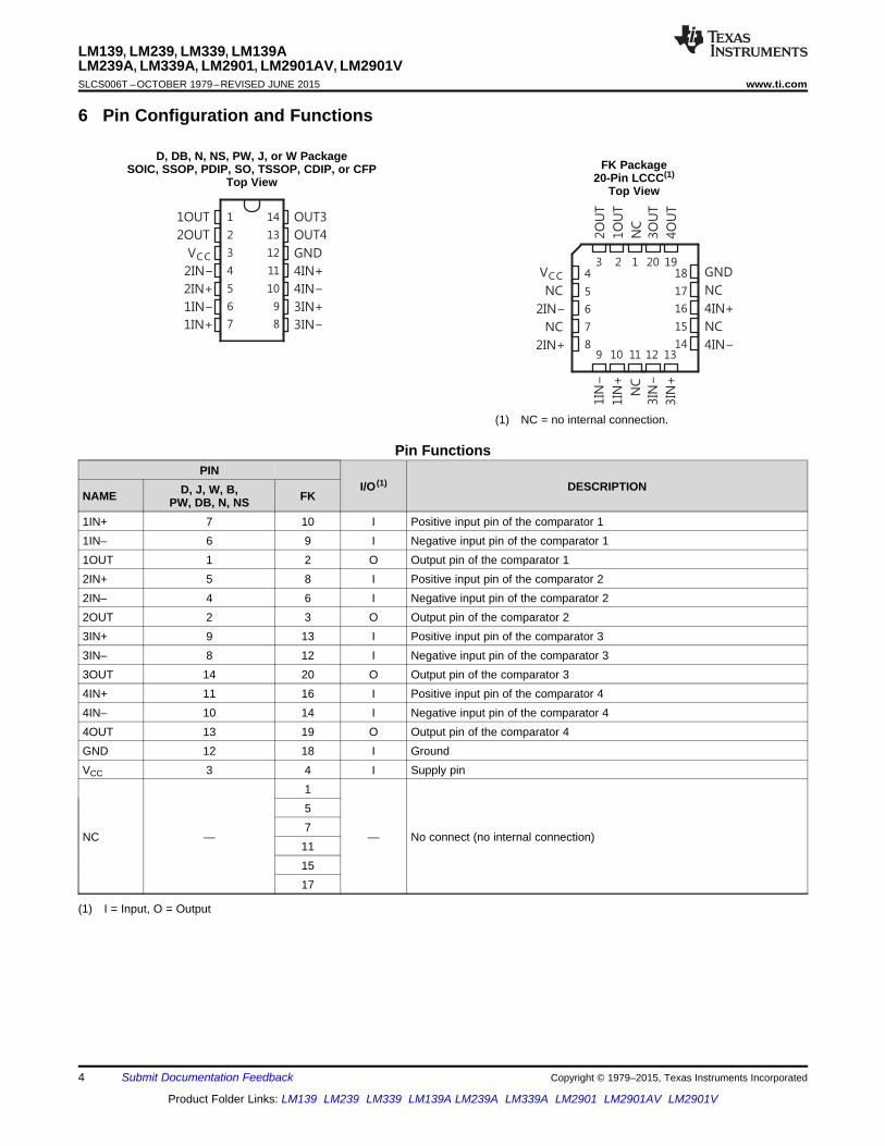
6 Pin Configuration and Functions
D, DB, N, NS, PW, J, or W PackageFK PackageSOIC, SSOP, PDIP, SO, TSSOP, CDIP, or CFP
20-Pin LCCC(1)Top View
Top View
(1) NC = no internal connection.
Pin FunctionsPIN
I/O (1) DESCRIPTIOND, J, W, B,NAME FKPW, DB, N, NS1IN+ 7 10 I Positive input pin of the comparator 11IN– 6 9 I Negative input pin of the comparator 11OUT 1 2 O Output pin of the comparator 12IN+ 5 8 I Positive input pin of the comparator 22IN– 4 6 I Negative input pin of the comparator 22OUT 2 3 O Output pin of the comparator 23IN+ 9 13 I Positive input pin of the comparator 33IN– 8 12 I Negative input pin of the comparator 33OUT 14 20 O Output pin of the comparator 34IN+ 11 16 I Positive input pin of the comparator 44IN– 10 14 I Negative input pin of the comparator 44OUT 13 19 O Output pin of the comparator 4GND 12 18 I GroundVCC 3 4 I Supply pin
157
NC — — No connect (no internal connection)111517
(1) I = Input, O = Output
4 Submit Documentation Feedback Copyright © 1979–2015, Texas Instruments Incorporated
Product Folder Links: LM139 LM239 LM339 LM139A LM239A LM339A LM2901 LM2901AV LM2901V
LM139, LM239, LM339, LM139ALM239A, LM339A, LM2901, LM2901AV, LM2901V
www.ti.com SLCS006T –OCTOBER 1979–REVISED JUNE 2015
7 Specifications
7.1 Absolute Maximum Ratingsover operating free-air temperature range (unless otherwise noted) (1)
MIN MAX UNITVCC Supply voltage (2) 36 VVID Differential input voltage (3) ±36 VVI Input voltage range (either input) –0.3 36 VVO Output voltage 36 VIO Output current 20 mA
Duration of output short circuit to ground (4) UnlimitedTJ Operating virtual-junction temperature 150 °C
Case temperature for 60 s FK package 260 °CLead temperature 1.6 mm (1/16 in) from case for 60 s J package 300 °C
Tstg Storage temperature –65 150 °C
(1) Stresses beyond those listed under Absolute Maximum Ratings may cause permanent damage to the device. These are stress ratingsonly, and functional operation of the device at these or any other conditions beyond those indicated under Recommended OperatingConditions is not implied. Exposure to absolute-maximum-rated conditions for extended periods may affect device reliability.
(2) All voltage values, except differential voltages, are with respect to network ground.(3) Differential voltages are at xIN+ with respect to xIN–.(4) Short circuits from outputs to VCC can cause excessive heating and eventual destruction.
7.2 ESD RatingsVALUE UNIT
Human body model (HBM), per ANSI/ESDA/JEDEC JS-001 (1) ±500V(ESD) Electrostatic discharge VCharged-device model (CDM), per JEDEC specification JESD22- ±750C101 (2)
(1) JEDEC document JEP155 states that 500-V HBM allows safe manufacturing with a standard ESD control process.(2) JEDEC document JEP157 states that 250-V CDM allows safe manufacturing with a standard ESD control process.
7.3 Recommended Operating Conditionsover operating free-air temperature range (unless otherwise noted)
MIN MAX UNITNon-V devices 2 30 V
VCC Supply voltageV devices 2 32 V
TJ Junction temperature –40 125 °C
7.4 Thermal Information (14-Pin Packages)LMx39, LM2901
THERMAL METRIC (1) UNITD DB N NS PW J W(SOIC) (SSOP) (PDIP) (SO) (TSSOP) (CDIP) (CFP)
RθJA Junction-to-ambient thermal resistance 86 96 80 76 113 °C/WRθJC(top) Junction-to-case (top) thermal resistance 15.05 14.65 °C/W
(1) For more information about traditional and new thermal metrics, see the Semiconductor and IC Package Thermal Metrics applicationreport, SPRA953.
7.5 Thermal Information (20-Pin Packages)LMx39, LM2901
THERMAL METRIC (1) UNITFK (LCCC)
RθJC(top) Junction-to-case (top) thermal resistance 5.61 °C/W
(1) For more information about traditional and new thermal metrics, see the Semiconductor and IC Package Thermal Metrics applicationreport, SPRA953.
Copyright © 1979–2015, Texas Instruments Incorporated Submit Documentation Feedback 5
Product Folder Links: LM139 LM239 LM339 LM139A LM239A LM339A LM2901 LM2901AV LM2901V
LM139, LM239, LM339, LM139ALM239A, LM339A, LM2901, LM2901AV, LM2901VSLCS006T –OCTOBER 1979–REVISED JUNE 2015 www.ti.com
7.6 Electrical Characteristics for LM139 and LM139Aat specified free-air temperature, VCC = 5 V (unless otherwise noted)
LM139 LM139APARAMETER TEST CONDITIONS (1) TA
(2) UNITMIN TYP MAX MIN TYP MAX
VCC = 5 V to 30 V, 25°C 2 5 1 2VIO Input offset voltage VIC = VICR min, mV
Full range 9 4VO = 1.4 V25°C 3 25 3 25
IIO Input offset current VO = 1.4 V nAFull range 100 100
25°C –25 –100 –25 –100IIB Input bias current VO = 1.4 V nA
Full range –300 –3000 to 0 to25°C VCC – 1.5 VCC – 1.5Common-mode input-VICR Vvoltage range (3) 0 to 0 toFull range VCC – 2 VCC – 2
Large-signal differential- VCC+ = ±7.5 V,AVD 25°C 200 50 200 V/mVvoltage amplification VO = –5 V to 5 VVOH = 5 V 25°C 0.1 0.1 nA
IOH High-level output current VID = 1 VVOH = 30 V Full range 1 1 μA
25°C 150 400 150 400VOL Low-level output voltage VID = –1 V, IOL = 4 mA mV
Full range 700 700IOL Low-level output current VID = –1 V, VOL = 1.5 V 25°C 6 16 6 16 mA
Supply currentICC VO = 2.5 V, No load 25°C 0.8 2 0.8 2 mA(four comparators)
(1) All characteristics are measured with zero common-mode input voltage, unless otherwise specified.(2) Full range (MIN to MAX) for LM139 and LM139A is –55°C to 125°C. All characteristics are measured with zero common-mode input
voltage, unless otherwise specified.(3) The voltage at either input or common-mode must not be allowed to go negative by more than 0.3 V. The upper end of the common-
mode voltage range is VCC+ – 1.5 V; however, one input can exceed VCC, and the comparator will provide a proper output state as longas the other input remains in the common-mode range. Either or both inputs can go to 30 V without damage.
7.7 Electrical Characteristics for LMx39 and LMx39Aat specified free-air temperature, VCC = 5 V (unless otherwise noted)
LM239 LM239ALM339 LM339APARAMETER TEST CONDITIONS (1) TA
(2) UNITMIN TYP MAX MIN TYP MAX
VCC = 5 V to 30 V, 25°C 2 5 1 3VIO Input offset voltage VIC = VICR min, mV
Full range 9 4VO = 1.4 V25°C 5 50 5 50
IIO Input offset current VO = 1.4 V nAFull range 150 150
25°C –25 –250 –25 –250IIB Input bias current VO = 1.4 V nA
Full range –400 –4000 to 0 to25°C VCC – 1.5 VCC – 1.5Common-mode input-VICR Vvoltage range (3) 0 to 0 toFull range VCC – 2 VCC – 2
VCC = 15 V,Large-signal differential-AVD VO = 1.4 V to 11.4 V, 25°C 50 200 50 200 V/mVvoltage amplification RL ≥ 15 kΩ to VCC
(1) All characteristics are measured with zero common-mode input voltage, unless otherwise specified.(2) Full range (MIN to MAX) for LM239/LM239A is –25°C to 85°C, and for LM339/LM339A is 0°C to 70°C. All characteristics are measured
with zero common-mode input voltage, unless otherwise specified.(3) The voltage at either input or common-mode must not be allowed to go negative by more than 0.3 V. The upper end of the common-
mode voltage range is VCC+ – 1.5 V; however, one input can exceed VCC, and the comparator will provide a proper output state as longas the other input remains in the common-mode range. Either or both inputs can go to 30 V without damage.
6 Submit Documentation Feedback Copyright © 1979–2015, Texas Instruments Incorporated
Product Folder Links: LM139 LM239 LM339 LM139A LM239A LM339A LM2901 LM2901AV LM2901V
LM139, LM239, LM339, LM139ALM239A, LM339A, LM2901, LM2901AV, LM2901V
www.ti.com SLCS006T –OCTOBER 1979–REVISED JUNE 2015
Electrical Characteristics for LMx39 and LMx39A (continued)at specified free-air temperature, VCC = 5 V (unless otherwise noted)
LM239 LM239ALM339 LM339APARAMETER TEST CONDITIONS (1) TA
(2) UNITMIN TYP MAX MIN TYP MAX
VOH = 5 V 25°C 0.1 50 0.1 50 nAIOH High-level output current VID = 1 V
VOH = 30 V Full range 1 1 μA25°C 150 400 150 400
VOL Low-level output voltage VID = –1 V, IOL = 4 mA mVFull range 700 700
IOL Low-level output current VID = –1 V, VOL = 1.5 V 25°C 6 16 6 16 mASupply currentICC VO = 2.5 V, No load 25°C 0.8 2 0.8 2 mA(four comparators)
7.8 Electrical Characteristics for LM2901at specified free-air temperature, VCC = 5 V (unless otherwise noted)
LM2901PARAMETER TEST CONDITIONS (1) TA
(2) UNITMIN TYP MAX
25°C 2 7Non-A devicesVIC = VICR min, Full range 15
VIO Input offset voltage VO = 1.4 V, mV25°C 1 2VCC = 5 V to MAX (3)
A-suffix devicesFull range 4
25°C 5 50IIO Input offset current VO = 1.4 V nA
Full range 20025°C –25 –250
IIB Input bias current VO = 1.4 V nAFull range –500
0 to25°C VCC – 1.5Common-mode input-VICR Vvoltage range (4) 0 toFull range VCC – 2Large-signal differential- VCC = 15 V, VO = 1.4 V to 11.4 V,AVD 25°C 25 100 V/mVvoltage amplification RL ≥ 15 kΩ to VCC
VOH = 5 V 25°C 0.1 50 nAIOH High-level output current VID = 1 V
VOH = VCC MAX (3) Full range 1 μANon-V devices 150 500
25°CVID = –1 V,VOL Low-level output voltage V-suffix devices 150 400 mVIOL = 4 mAAll devices Full range 700
IOL Low-level output current VID = –1 V, VOL = 1.5 V 25°C 6 16 mAVCC = 5 V 0.8 2Supply current VO = 2.5 V,ICC 25°C mA(four comparators) No load VCC = MAX (3) 1 2.5
(1) All characteristics are measured with zero common-mode input voltage, unless otherwise specified.(2) Full range (MIN to MAX) for LM2901 is –40°C to 125°C. All characteristics are measured with zero common-mode input voltage, unless
otherwise specified.(3) VCC MAX = 30 V for non-V devices, and 32 V for V-suffix devices(4) The voltage at either input or common-mode must not be allowed to go negative by more than 0.3 V. The upper end of the common-
mode voltage range is VCC+ – 1.5 V; however, one input can exceed VCC, and the comparator will provide a proper output state as longas the other input remains in the common-mode range. Either or both inputs can go to VCC MAX without damage.
Copyright © 1979–2015, Texas Instruments Incorporated Submit Documentation Feedback 7
Product Folder Links: LM139 LM239 LM339 LM139A LM239A LM339A LM2901 LM2901AV LM2901V

LM139, LM239, LM339, LM139ALM239A, LM339A, LM2901, LM2901AV, LM2901VSLCS006T –OCTOBER 1979–REVISED JUNE 2015 www.ti.com
7.9 Switching Characteristics for LM2901VCC = 5 V, TA = 25°C
LM2901PARAMETER TEST CONDITIONS UNIT
TYP100-mV input step with 5-mV overdrive 1.3RL connected to 5 V through 5.1 kΩ,Response time μsCL = 15 pF (1) (2) TTL-level input step 0.3
(1) CL includes probe and jig capacitance.(2) The response time specified is the interval between the input step function and the instant when the output crosses 1.4 V.
7.10 Switching Characteristics for LM139 and LM139AVCC = 5 V, TA = 25°C
LM139LM139APARAMETER TEST CONDITIONS UNIT
TYP100-mV input step with 5-mV overdrive 1.3RL connected to 5 V through 5.1 kΩ,Response time μsCL = 15 pF (1) (2) TTL-level input step 0.3
(1) CL includes probe and jig capacitance.(2) The response time specified is the interval between the input step function and the instant when the output crosses 1.4 V.
7.11 Switching Characteristics for LMx39 and LMx39AVCC = 5 V, TA = 25°C
LM239LM239ALM339PARAMETER TEST CONDITIONS UNIT
LM339ATYP
100-mV input step with 5-mV overdrive 1.3RL connected to 5 V through 5.1 kΩ,Response time μsCL = 15 pF (1) (2) TTL-level input step 0.3
(1) CL includes probe and jig capacitance.(2) The response time specified is the interval between the input step function and the instant when the output crosses 1.4 V.
8 Submit Documentation Feedback Copyright © 1979–2015, Texas Instruments Incorporated
Product Folder Links: LM139 LM239 LM339 LM139A LM239A LM339A LM2901 LM2901AV LM2901V
-1
0
1
2
3
4
5
6
-0.3 0 0.25 0.5 0.75 1 1.25 1.5 1.75 2 2.25
t – Time – µs
VO
–O
utp
ut
Vo
ltag
e–
V
Overdrive = 5 mV
Overdrive = 100 mV
Overdrive = 20 mV
0.001
0.01
0.1
1
10
0.01 0.1 1 10 100
IO – Output Sink Current – mA
VO
–S
atu
rati
on
Vo
ltag
e–
V
T = –55°CA
T = 25°CA
T = 125°CA
-1
0
1
2
3
4
5
6
-0.3 0 0.25 0.5 0.75 1 1.25 1.5 1.75 2 2.25
t – Time – µs
VO
–O
utp
ut
Vo
ltag
e–
V
Overdrive = 5 mV
Overdrive = 100 mV
Overdrive = 20 mV
0
0.2
0.4
0.6
0.8
1
1.2
1.4
1.6
1.8
0 5 10 15 20 25 30 35
VCC – Supply Voltage – V
I CC
–S
up
ply
Cu
rren
t–
mA
T = –55°CA
T = 0°CA
T = 25°CA
T = 70°CA
T = 125°CA
0
10
20
30
40
50
60
70
80
0 5 10 15 20 25 30 35
VCC – Supply Voltage – V
I IN–
Inp
ut
Bia
sC
urr
en
t–
nA
T = –55°CA
T = 0°CA
T = 25°CA
T = 70°CA
T = 125°CA
LM139, LM239, LM339, LM139ALM239A, LM339A, LM2901, LM2901AV, LM2901V
www.ti.com SLCS006T –OCTOBER 1979–REVISED JUNE 2015
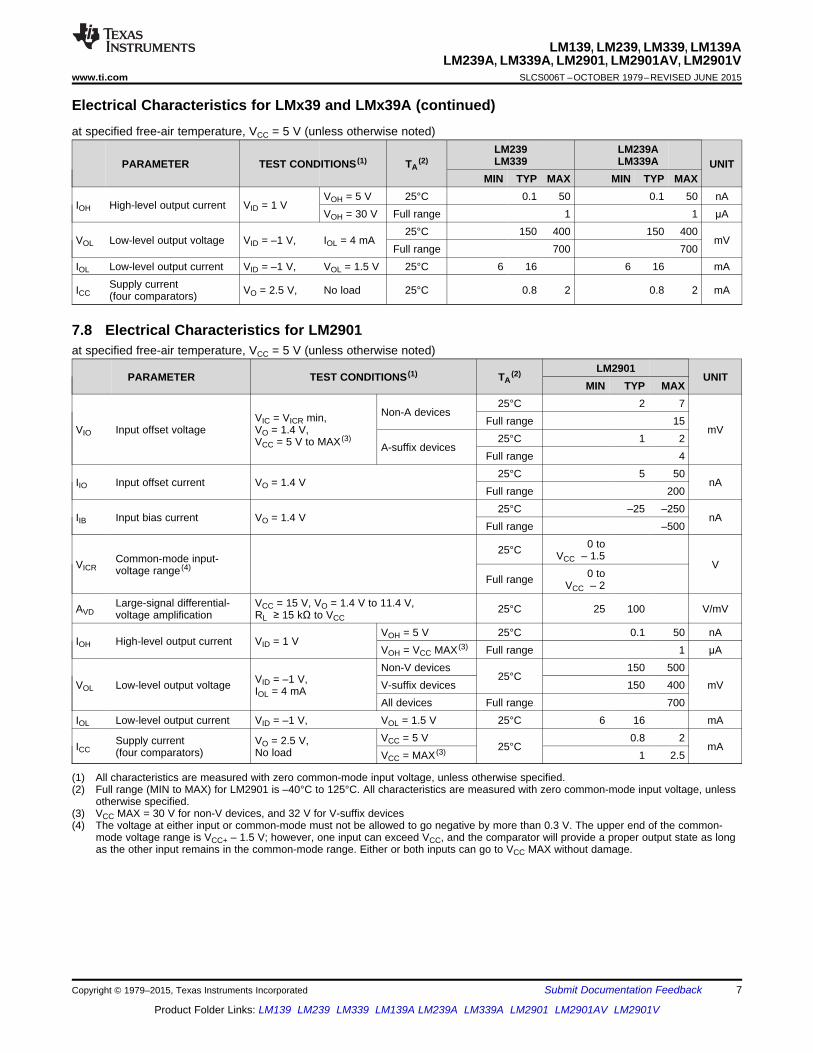
7.12 Typical Characteristics
Figure 1. Supply Current vs Supply Voltage Figure 2. Input Bias Current vs Supply Voltage
Figure 4. Response Time for Various OverdrivesFigure 3. Output Saturation VoltageNegative Transition
Figure 5. Response Time for Various OverdrivesPositive Transition
Copyright © 1979–2015, Texas Instruments Incorporated Submit Documentation Feedback 9
Product Folder Links: LM139 LM239 LM339 LM139A LM239A LM339A LM2901 LM2901AV LM2901V
80- Aµ
Current Regulator
80 µA60 µA 10 µA
VCC
10 µA
OUT
GND
IN+
IN−
Epi-FET
Diodes
Resistors
Transistors
COMPONENT COUNT
1
2
2
30
LM139, LM239, LM339, LM139ALM239A, LM339A, LM2901, LM2901AV, LM2901VSLCS006T –OCTOBER 1979–REVISED JUNE 2015 www.ti.com
8 Detailed Description
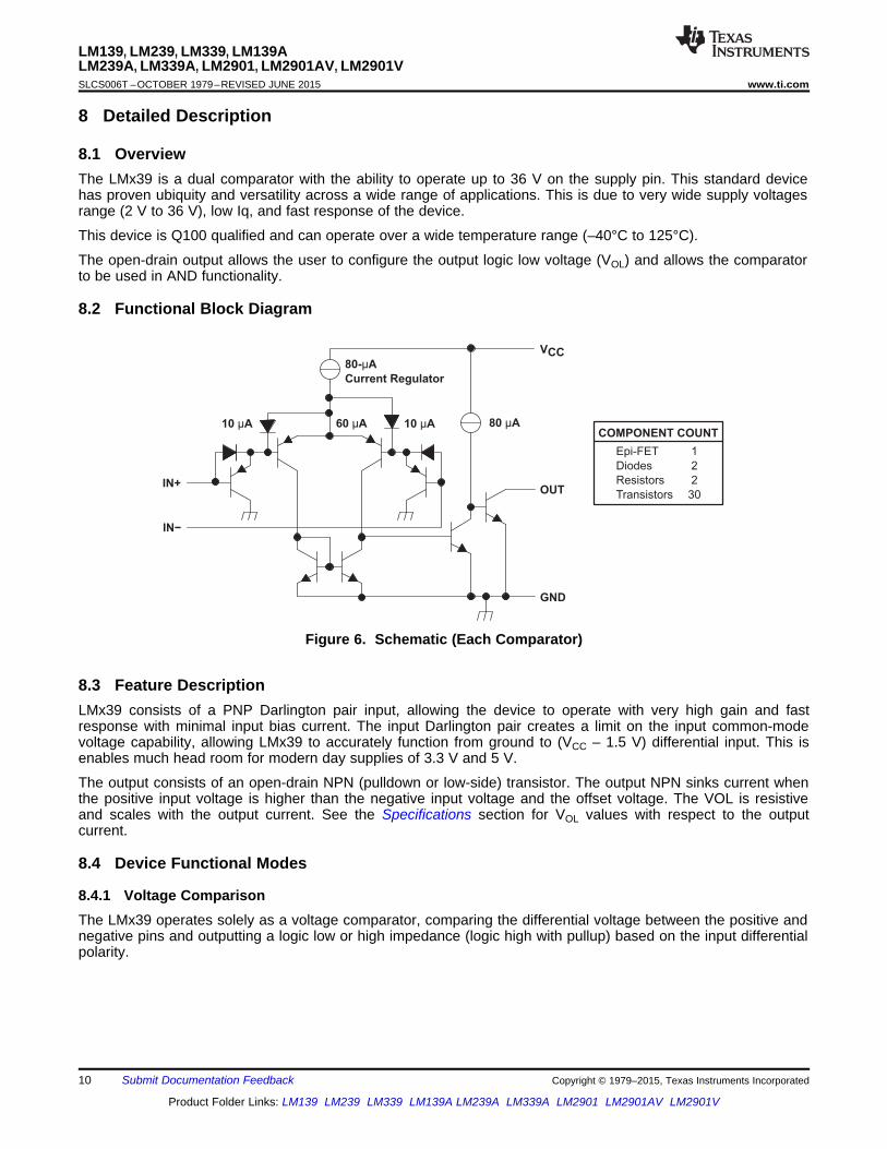
8.1 OverviewThe LMx39 is a dual comparator with the ability to operate up to 36 V on the supply pin. This standard devicehas proven ubiquity and versatility across a wide range of applications. This is due to very wide supply voltagesrange (2 V to 36 V), low Iq, and fast response of the device.
This device is Q100 qualified and can operate over a wide temperature range (–40°C to 125°C).
The open-drain output allows the user to configure the output logic low voltage (VOL) and allows the comparatorto be used in AND functionality.
8.2 Functional Block Diagram
Figure 6. Schematic (Each Comparator)
8.3 Feature DescriptionLMx39 consists of a PNP Darlington pair input, allowing the device to operate with very high gain and fastresponse with minimal input bias current. The input Darlington pair creates a limit on the input common-modevoltage capability, allowing LMx39 to accurately function from ground to (VCC – 1.5 V) differential input. This isenables much head room for modern day supplies of 3.3 V and 5 V.
The output consists of an open-drain NPN (pulldown or low-side) transistor. The output NPN sinks current whenthe positive input voltage is higher than the negative input voltage and the offset voltage. The VOL is resistiveand scales with the output current. See the Specifications section for VOL values with respect to the outputcurrent.
8.4 Device Functional Modes
8.4.1 Voltage ComparisonThe LMx39 operates solely as a voltage comparator, comparing the differential voltage between the positive andnegative pins and outputting a logic low or high impedance (logic high with pullup) based on the input differentialpolarity.
10 Submit Documentation Feedback Copyright © 1979–2015, Texas Instruments Incorporated
Product Folder Links: LM139 LM239 LM339 LM139A LM239A LM339A LM2901 LM2901AV LM2901V

+LM2901
VLOGIC
VSUP
Vref
Vin +LM2901
Vin-
Vin+
RpullupRpullup
VLOGIC
VSUP
CL CL
LM139, LM239, LM339, LM139ALM239A, LM339A, LM2901, LM2901AV, LM2901V
www.ti.com SLCS006T –OCTOBER 1979–REVISED JUNE 2015
9 Application and Implementation
NOTEInformation in the following applications sections is not part of the TI componentspecification, and TI does not warrant its accuracy or completeness. TI’s customers areresponsible for determining suitability of components for their purposes. Validate and testthe design implementation to confirm system functionality.
9.1 Application InformationTypically, the LMx39 compares either a single signal to a reference or two signals. Many users take advantage ofthe open-drain output to drive the comparison logic output to a logic voltage level to an MCU or logic device. Thewide supply range and high voltage capability makes LMx39 optimal for level shifting to a higher or lower voltage.
9.2 Typical Application
Figure 7. Single-ended and Differential Comparator Configurations
9.2.1 Design RequirementsFor this design example, use the parameters listed in Table 1 as the input parameters.
Table 1. Design ParametersDESIGN PARAMETER EXAMPLE VALUE
Input Voltage Range 0 V to Vsup-1.5 VSupply Voltage 2 V to 36 V
Logic Supply Voltage 2 V to 36 VOutput Current (RPULLUP) 1 µA to 20 mAInput Overdrive Voltage 100 mV
Reference Voltage 2.5 VLoad Capacitance (CL) 15 pF
9.2.2 Detailed Design ProcedureWhen using LMx39 in a general comparator application, determine the following:• Input voltage range• Minimum overdrive voltage• Output and drive current• Response time
9.2.2.1 Input Voltage RangeWhen choosing the input voltage range, the input common-mode voltage range (VICR) must be taken in toaccount. If temperature operation is above or below 25°C the VICR can range from 0 V to VCC– 2 V. This limitsthe input voltage range to as high as VCC– 2 V and as low as 0 V. Operation outside of this range can yieldincorrect comparisons.
Copyright © 1979–2015, Texas Instruments Incorporated Submit Documentation Feedback 11
Product Folder Links: LM139 LM239 LM339 LM139A LM239A LM339A LM2901 LM2901AV LM2901V
OLCE
OUT
VR
I=
N CE LR Ct @ ´
P PULLUP LR Ct @ ´
LM139, LM239, LM339, LM139ALM239A, LM339A, LM2901, LM2901AV, LM2901VSLCS006T –OCTOBER 1979–REVISED JUNE 2015 www.ti.com
The following list describes the outcomes of some input voltage situations.
• When both IN– and IN+ are both within the common-mode range:– If IN– is higher than IN+ and the offset voltage, the output is low and the output transistor is sinking
current– If IN– is lower than IN+ and the offset voltage, the output is high impedance and the output transistor is
not conducting• When IN– is higher than common mode and IN+ is within common mode, the output is low and the output
transistor is sinking current• When IN+ is higher than common mode and IN– is within common mode, the output is high impedance and
the output transistor is not conducting• When IN– and IN+ are both higher than common mode, the output is low and the output transistor is sinking
current
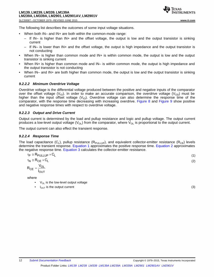
9.2.2.2 Minimum Overdrive VoltageOverdrive voltage is the differential voltage produced between the positive and negative inputs of the comparatorover the offset voltage (VIO). In order to make an accurate comparison, the overdrive voltage (VOD) must behigher than the input offset voltage (VIO). Overdrive voltage can also determine the response time of thecomparator, with the response time decreasing with increasing overdrive. Figure 8 and Figure 9 show positiveand negative response times with respect to overdrive voltage.
9.2.2.3 Output and Drive CurrentOutput current is determined by the load and pullup resistance and logic and pullup voltage. The output currentproduces a low-level output voltage (VOL) from the comparator, where VOL is proportional to the output current.
The output current can also effect the transient response.
9.2.2.4 Response TimeThe load capacitance (CL), pullup resistance (RPULLUP), and equivalent collector-emitter resistance (RCE) levelsdetermine the transient response. Equation 1 approximates the positive response time. Equation 2 approximatesthe negative response time. Equation 3 calculates the collector-emitter resistance.
(1)
(2)
where• VOL is the low-level output voltage• IOUT is the output current (3)
12 Submit Documentation Feedback Copyright © 1979–2015, Texas Instruments Incorporated
Product Folder Links: LM139 LM239 LM339 LM139A LM239A LM339A LM2901 LM2901AV LM2901V
1OUT 1
1INí
2
1IN+
3 GND4
VCC
7
2OUT
6
2INí
5
2IN+
0.1PF
Ground
Bypass
Capacitor
Negative Supply or GroundPositive Supply
0.1PF
Ground
Only needed for dual power
supplies
14
13
12
11
8
9
10
3INí3IN+
4INí4IN+
3OUT4OUT
±1
0
1
2
3
4
5
6
-0.25 0.25 0.75 1.25 1.75 2.25
Out
put V
olta
ge,
Vo(
V)
Time (usec)
5mV OD
20mV OD
100mV OD
C004
±1
0
1
2
3
4
5
6
±0.25 0.00 0.25 0.50 0.75 1.00 1.25 1.50 1.75 2.00
Out
put V
olta
ge (
Vo)
Time (usec)
5mV OD
20mV OD
100mV OD
C006
LM139, LM239, LM339, LM139ALM239A, LM339A, LM2901, LM2901AV, LM2901V
www.ti.com SLCS006T –OCTOBER 1979–REVISED JUNE 2015
9.2.3 Application CurvesFigure 8 and Figure 9 were generated with scope probe parasitic capacitance of 50 pF.
VCC = 5 V VLogic = 5 V RPULLUP = 5.1 kΩ VCC = 5 V VLogic = 5 V RPULLUP = 5.1 kΩ
Figure 8. Response Time vs Output Voltage Figure 9. Response Time vs Output Voltage(Positive Transition) (Negative Transition)
10 Power Supply RecommendationsFor fast response and comparison applications with noisy or AC inputs, use a bypass capacitor on the supply pinto reject any variation on the supply voltage. This variation can affect the common-mode range of the comparatorinput and create an inaccurate comparison.
11 Layout
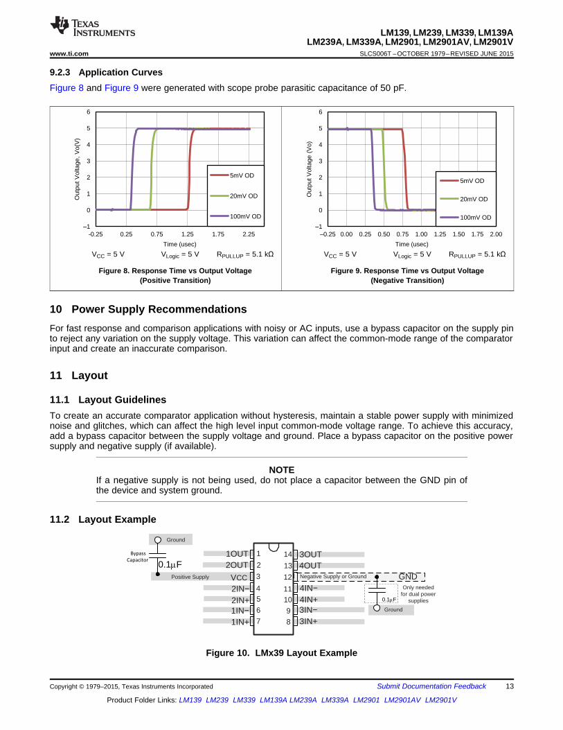
11.1 Layout GuidelinesTo create an accurate comparator application without hysteresis, maintain a stable power supply with minimizednoise and glitches, which can affect the high level input common-mode voltage range. To achieve this accuracy,add a bypass capacitor between the supply voltage and ground. Place a bypass capacitor on the positive powersupply and negative supply (if available).
NOTEIf a negative supply is not being used, do not place a capacitor between the GND pin ofthe device and system ground.
11.2 Layout Example
Figure 10. LMx39 Layout Example
Copyright © 1979–2015, Texas Instruments Incorporated Submit Documentation Feedback 13
Product Folder Links: LM139 LM239 LM339 LM139A LM239A LM339A LM2901 LM2901AV LM2901V
LM139, LM239, LM339, LM139ALM239A, LM339A, LM2901, LM2901AV, LM2901VSLCS006T –OCTOBER 1979–REVISED JUNE 2015 www.ti.com
12 Device and Documentation Support
12.1 Related LinksThe table below lists quick access links. Categories include technical documents, support and communityresources, tools and software, and quick access to sample or buy.
Table 2. Related LinksTECHNICAL TOOLS & SUPPORT &PARTS PRODUCT FOLDER SAMPLE & BUY DOCUMENTS SOFTWARE COMMUNITY
LM139 Click here Click here Click here Click here Click hereLM239 Click here Click here Click here Click here Click hereLM339 Click here Click here Click here Click here Click here
LM139A Click here Click here Click here Click here Click hereLM239A Click here Click here Click here Click here Click hereLM339A Click here Click here Click here Click here Click hereLM2901 Click here Click here Click here Click here Click here
LM2901AV Click here Click here Click here Click here Click hereLM2901V Click here Click here Click here Click here Click here
12.2 Community ResourcesThe following links connect to TI community resources. Linked contents are provided "AS IS" by the respectivecontributors. They do not constitute TI specifications and do not necessarily reflect TI's views; see TI's Terms ofUse.
TI E2E™ Online Community TI's Engineer-to-Engineer (E2E) Community. Created to foster collaborationamong engineers. At e2e.ti.com, you can ask questions, share knowledge, explore ideas and helpsolve problems with fellow engineers.
Design Support TI's Design Support Quickly find helpful E2E forums along with design support tools andcontact information for technical support.
12.3 TrademarksE2E is a trademark of Texas Instruments.All other trademarks are the property of their respective owners.
12.4 Electrostatic Discharge CautionThese devices have limited built-in ESD protection. The leads should be shorted together or the device placed in conductive foamduring storage or handling to prevent electrostatic damage to the MOS gates.
12.5 GlossarySLYZ022 — TI Glossary.
This glossary lists and explains terms, acronyms, and definitions.
13 Mechanical, Packaging, and Orderable InformationThe following pages include mechanical packaging and orderable information. This information is the mostcurrent data available for the designated devices. This data is subject to change without notice and revision ofthis document. For browser based versions of this data sheet, refer to the left hand navigation.
14 Submit Documentation Feedback Copyright © 1979–2015, Texas Instruments Incorporated
Product Folder Links: LM139 LM239 LM339 LM139A LM239A LM339A LM2901 LM2901AV LM2901V
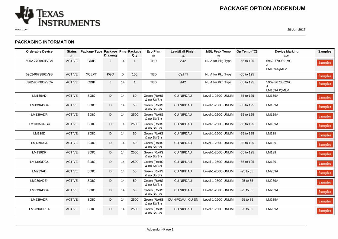
PACKAGE OPTION ADDENDUM
www.ti.com 29-Jun-2017
Addendum-Page 1
PACKAGING INFORMATION
Orderable Device Status(1)
Package Type PackageDrawing
Pins PackageQty
Eco Plan(2)
Lead/Ball Finish(6)
MSL Peak Temp(3)
Op Temp (°C) Device Marking(4/5)
Samples
5962-7700801VCA ACTIVE CDIP J 14 1 TBD A42 N / A for Pkg Type -55 to 125 5962-7700801VCALM139JQMLV
5962-9673802V9B ACTIVE XCEPT KGD 0 100 TBD Call TI N / A for Pkg Type -55 to 125
5962-9673802VCA ACTIVE CDIP J 14 1 TBD A42 N / A for Pkg Type -55 to 125 5962-9673802VCALM139AJQMLV
LM139AD ACTIVE SOIC D 14 50 Green (RoHS& no Sb/Br)
CU NIPDAU Level-1-260C-UNLIM -55 to 125 LM139A
LM139ADG4 ACTIVE SOIC D 14 50 Green (RoHS& no Sb/Br)
CU NIPDAU Level-1-260C-UNLIM -55 to 125 LM139A
LM139ADR ACTIVE SOIC D 14 2500 Green (RoHS& no Sb/Br)
CU NIPDAU Level-1-260C-UNLIM -55 to 125 LM139A
LM139ADRG4 ACTIVE SOIC D 14 2500 Green (RoHS& no Sb/Br)
CU NIPDAU Level-1-260C-UNLIM -55 to 125 LM139A
LM139D ACTIVE SOIC D 14 50 Green (RoHS& no Sb/Br)
CU NIPDAU Level-1-260C-UNLIM -55 to 125 LM139
LM139DG4 ACTIVE SOIC D 14 50 Green (RoHS& no Sb/Br)
CU NIPDAU Level-1-260C-UNLIM -55 to 125 LM139
LM139DR ACTIVE SOIC D 14 2500 Green (RoHS& no Sb/Br)
CU NIPDAU Level-1-260C-UNLIM -55 to 125 LM139
LM139DRG4 ACTIVE SOIC D 14 2500 Green (RoHS& no Sb/Br)
CU NIPDAU Level-1-260C-UNLIM -55 to 125 LM139
LM239AD ACTIVE SOIC D 14 50 Green (RoHS& no Sb/Br)
CU NIPDAU Level-1-260C-UNLIM -25 to 85 LM239A
LM239ADE4 ACTIVE SOIC D 14 50 Green (RoHS& no Sb/Br)
CU NIPDAU Level-1-260C-UNLIM -25 to 85 LM239A
LM239ADG4 ACTIVE SOIC D 14 50 Green (RoHS& no Sb/Br)
CU NIPDAU Level-1-260C-UNLIM -25 to 85 LM239A
LM239ADR ACTIVE SOIC D 14 2500 Green (RoHS& no Sb/Br)
CU NIPDAU | CU SN Level-1-260C-UNLIM -25 to 85 LM239A
LM239ADRE4 ACTIVE SOIC D 14 2500 Green (RoHS& no Sb/Br)
CU NIPDAU Level-1-260C-UNLIM -25 to 85 LM239A

PACKAGE OPTION ADDENDUM
www.ti.com 29-Jun-2017
Addendum-Page 2
Orderable Device Status(1)
Package Type PackageDrawing
Pins PackageQty
Eco Plan(2)
Lead/Ball Finish(6)
MSL Peak Temp(3)
Op Temp (°C) Device Marking(4/5)
Samples
LM239ADRG4 ACTIVE SOIC D 14 2500 Green (RoHS& no Sb/Br)
CU NIPDAU Level-1-260C-UNLIM -25 to 85 LM239A
LM239D ACTIVE SOIC D 14 50 Green (RoHS& no Sb/Br)
CU NIPDAU Level-1-260C-UNLIM -25 to 85 LM239
LM239DE4 ACTIVE SOIC D 14 50 Green (RoHS& no Sb/Br)
CU NIPDAU Level-1-260C-UNLIM -25 to 85 LM239
LM239DG4 ACTIVE SOIC D 14 50 Green (RoHS& no Sb/Br)
CU NIPDAU Level-1-260C-UNLIM -25 to 85 LM239
LM239DR ACTIVE SOIC D 14 2500 Green (RoHS& no Sb/Br)
CU NIPDAU | CU SN Level-1-260C-UNLIM -25 to 85 LM239
LM239DRG3 ACTIVE SOIC D 14 2500 Green (RoHS& no Sb/Br)
CU SN Level-1-260C-UNLIM -25 to 85 LM239
LM239DRG4 ACTIVE SOIC D 14 2500 Green (RoHS& no Sb/Br)
CU NIPDAU Level-1-260C-UNLIM -25 to 85 LM239
LM239N ACTIVE PDIP N 14 25 Pb-Free(RoHS)
CU NIPDAU | CU SN N / A for Pkg Type -25 to 85 LM239N
LM239NE4 ACTIVE PDIP N 14 25 Pb-Free(RoHS)
CU NIPDAU N / A for Pkg Type -25 to 85 LM239N
LM239PW ACTIVE TSSOP PW 14 90 Green (RoHS& no Sb/Br)
CU NIPDAU Level-1-260C-UNLIM -25 to 85 L239
LM239PWG4 ACTIVE TSSOP PW 14 90 Green (RoHS& no Sb/Br)
CU NIPDAU Level-1-260C-UNLIM -25 to 85 L239
LM239PWR ACTIVE TSSOP PW 14 2000 Green (RoHS& no Sb/Br)
CU NIPDAU | CU SN Level-1-260C-UNLIM -25 to 85 L239
LM239PWRE4 ACTIVE TSSOP PW 14 2000 Green (RoHS& no Sb/Br)
CU NIPDAU Level-1-260C-UNLIM -25 to 85 L239
LM239PWRG4 ACTIVE TSSOP PW 14 2000 Green (RoHS& no Sb/Br)
CU NIPDAU Level-1-260C-UNLIM -25 to 85 L239
LM2901AVQDR ACTIVE SOIC D 14 2500 Green (RoHS& no Sb/Br)
CU NIPDAU Level-1-260C-UNLIM -40 to 125 L2901AV
LM2901AVQDRG4 ACTIVE SOIC D 14 2500 Green (RoHS& no Sb/Br)
CU NIPDAU Level-1-260C-UNLIM -40 to 125 L2901AV
LM2901AVQPWR ACTIVE TSSOP PW 14 2000 Green (RoHS& no Sb/Br)
CU NIPDAU Level-1-260C-UNLIM -40 to 125 L2901AV
LM2901AVQPWRG4 ACTIVE TSSOP PW 14 2000 Green (RoHS& no Sb/Br)
CU NIPDAU Level-1-260C-UNLIM -40 to 125 L2901AV

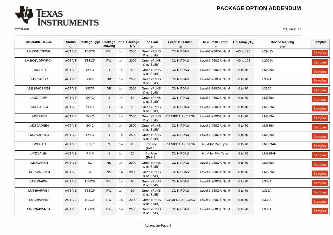
PACKAGE OPTION ADDENDUM
www.ti.com 29-Jun-2017
Addendum-Page 3
Orderable Device Status(1)
Package Type PackageDrawing
Pins PackageQty
Eco Plan(2)
Lead/Ball Finish(6)
MSL Peak Temp(3)
Op Temp (°C) Device Marking(4/5)
Samples
LM2901D ACTIVE SOIC D 14 50 Green (RoHS& no Sb/Br)
CU NIPDAU Level-1-260C-UNLIM -40 to 125 LM2901
LM2901DE4 ACTIVE SOIC D 14 50 Green (RoHS& no Sb/Br)
CU NIPDAU Level-1-260C-UNLIM -40 to 125 LM2901
LM2901DG4 ACTIVE SOIC D 14 50 Green (RoHS& no Sb/Br)
CU NIPDAU Level-1-260C-UNLIM -40 to 125 LM2901
LM2901DR ACTIVE SOIC D 14 2500 Green (RoHS& no Sb/Br)
CU NIPDAU | CU SN Level-1-260C-UNLIM -40 to 125 LM2901
LM2901DRE4 ACTIVE SOIC D 14 2500 Green (RoHS& no Sb/Br)
CU NIPDAU Level-1-260C-UNLIM -40 to 125 LM2901
LM2901DRG3 ACTIVE SOIC D 14 2500 Green (RoHS& no Sb/Br)
CU SN Level-1-260C-UNLIM -40 to 125 LM2901
LM2901DRG4 ACTIVE SOIC D 14 2500 Green (RoHS& no Sb/Br)
CU NIPDAU Level-1-260C-UNLIM -40 to 125 LM2901
LM2901N ACTIVE PDIP N 14 25 Pb-Free(RoHS)
CU NIPDAU N / A for Pkg Type -40 to 125 LM2901N
LM2901NE4 ACTIVE PDIP N 14 25 Pb-Free(RoHS)
CU NIPDAU N / A for Pkg Type -40 to 125 LM2901N
LM2901NSR ACTIVE SO NS 14 2000 Green (RoHS& no Sb/Br)
CU NIPDAU Level-1-260C-UNLIM -40 to 125 LM2901
LM2901NSRG4 ACTIVE SO NS 14 2000 Green (RoHS& no Sb/Br)
CU NIPDAU Level-1-260C-UNLIM -40 to 125 LM2901
LM2901PW ACTIVE TSSOP PW 14 90 Green (RoHS& no Sb/Br)
CU NIPDAU Level-1-260C-UNLIM -40 to 125 L2901
LM2901PWG4 ACTIVE TSSOP PW 14 90 Green (RoHS& no Sb/Br)
CU NIPDAU Level-1-260C-UNLIM -40 to 125 L2901
LM2901PWR ACTIVE TSSOP PW 14 2000 Green (RoHS& no Sb/Br)
CU NIPDAU | CU SN Level-1-260C-UNLIM -40 to 125 L2901
LM2901PWRG3 ACTIVE TSSOP PW 14 2000 Green (RoHS& no Sb/Br)
CU SN Level-1-260C-UNLIM -40 to 125 L2901
LM2901PWRG4 ACTIVE TSSOP PW 14 2000 Green (RoHS& no Sb/Br)
CU NIPDAU Level-1-260C-UNLIM -40 to 125 L2901
LM2901VQDR ACTIVE SOIC D 14 2500 Green (RoHS& no Sb/Br)
CU NIPDAU Level-1-260C-UNLIM -40 to 125 L2901V
LM2901VQDRG4 ACTIVE SOIC D 14 2500 Green (RoHS& no Sb/Br)
CU NIPDAU Level-1-260C-UNLIM -40 to 125 L2901V
PACKAGE OPTION ADDENDUM
www.ti.com 29-Jun-2017
Addendum-Page 4
Orderable Device Status(1)
Package Type PackageDrawing
Pins PackageQty
Eco Plan(2)
Lead/Ball Finish(6)
MSL Peak Temp(3)
Op Temp (°C) Device Marking(4/5)
Samples
LM2901VQPWR ACTIVE TSSOP PW 14 2000 Green (RoHS& no Sb/Br)
CU NIPDAU Level-1-260C-UNLIM -40 to 125 L2901V
LM2901VQPWRG4 ACTIVE TSSOP PW 14 2000 Green (RoHS& no Sb/Br)
CU NIPDAU Level-1-260C-UNLIM -40 to 125 L2901V
LM339AD ACTIVE SOIC D 14 50 Green (RoHS& no Sb/Br)
CU NIPDAU Level-1-260C-UNLIM 0 to 70 LM339A
LM339ADBR ACTIVE SSOP DB 14 2000 Green (RoHS& no Sb/Br)
CU NIPDAU Level-1-260C-UNLIM 0 to 70 L339A
LM339ADBRG4 ACTIVE SSOP DB 14 2000 Green (RoHS& no Sb/Br)
CU NIPDAU Level-1-260C-UNLIM 0 to 70 L339A
LM339ADE4 ACTIVE SOIC D 14 50 Green (RoHS& no Sb/Br)
CU NIPDAU Level-1-260C-UNLIM 0 to 70 LM339A
LM339ADG4 ACTIVE SOIC D 14 50 Green (RoHS& no Sb/Br)
CU NIPDAU Level-1-260C-UNLIM 0 to 70 LM339A
LM339ADR ACTIVE SOIC D 14 2500 Green (RoHS& no Sb/Br)
CU NIPDAU | CU SN Level-1-260C-UNLIM 0 to 70 LM339A
LM339ADRE4 ACTIVE SOIC D 14 2500 Green (RoHS& no Sb/Br)
CU NIPDAU Level-1-260C-UNLIM 0 to 70 LM339A
LM339ADRG4 ACTIVE SOIC D 14 2500 Green (RoHS& no Sb/Br)
CU NIPDAU Level-1-260C-UNLIM 0 to 70 LM339A
LM339AN ACTIVE PDIP N 14 25 Pb-Free(RoHS)
CU NIPDAU | CU SN N / A for Pkg Type 0 to 70 LM339AN
LM339ANE4 ACTIVE PDIP N 14 25 Pb-Free(RoHS)
CU NIPDAU N / A for Pkg Type 0 to 70 LM339AN
LM339ANSR ACTIVE SO NS 14 2000 Green (RoHS& no Sb/Br)
CU NIPDAU Level-1-260C-UNLIM 0 to 70 LM339A
LM339ANSRG4 ACTIVE SO NS 14 2000 Green (RoHS& no Sb/Br)
CU NIPDAU Level-1-260C-UNLIM 0 to 70 LM339A
LM339APW ACTIVE TSSOP PW 14 90 Green (RoHS& no Sb/Br)
CU NIPDAU Level-1-260C-UNLIM 0 to 70 L339A
LM339APWG4 ACTIVE TSSOP PW 14 90 Green (RoHS& no Sb/Br)
CU NIPDAU Level-1-260C-UNLIM 0 to 70 L339A
LM339APWR ACTIVE TSSOP PW 14 2000 Green (RoHS& no Sb/Br)
CU NIPDAU | CU SN Level-1-260C-UNLIM 0 to 70 L339A
LM339APWRE4 ACTIVE TSSOP PW 14 2000 Green (RoHS& no Sb/Br)
CU NIPDAU Level-1-260C-UNLIM 0 to 70 L339A

PACKAGE OPTION ADDENDUM
www.ti.com 29-Jun-2017
Addendum-Page 5
Orderable Device Status(1)
Package Type PackageDrawing
Pins PackageQty
Eco Plan(2)
Lead/Ball Finish(6)
MSL Peak Temp(3)
Op Temp (°C) Device Marking(4/5)
Samples
LM339APWRG4 ACTIVE TSSOP PW 14 2000 Green (RoHS& no Sb/Br)
CU NIPDAU Level-1-260C-UNLIM 0 to 70 L339A
LM339D ACTIVE SOIC D 14 50 Green (RoHS& no Sb/Br)
CU NIPDAU Level-1-260C-UNLIM 0 to 70 LM339
LM339DBR ACTIVE SSOP DB 14 2000 Green (RoHS& no Sb/Br)
CU NIPDAU Level-1-260C-UNLIM 0 to 70 LM339
LM339DBRE4 ACTIVE SSOP DB 14 2000 Green (RoHS& no Sb/Br)
CU NIPDAU Level-1-260C-UNLIM 0 to 70 LM339
LM339DE4 ACTIVE SOIC D 14 50 Green (RoHS& no Sb/Br)
CU NIPDAU Level-1-260C-UNLIM 0 to 70 LM339
LM339DG4 ACTIVE SOIC D 14 50 Green (RoHS& no Sb/Br)
CU NIPDAU Level-1-260C-UNLIM 0 to 70 LM339
LM339DR ACTIVE SOIC D 14 2500 Green (RoHS& no Sb/Br)
CU NIPDAU | CU SN Level-1-260C-UNLIM 0 to 70 LM339
LM339DRE4 ACTIVE SOIC D 14 2500 Green (RoHS& no Sb/Br)
CU NIPDAU Level-1-260C-UNLIM 0 to 70 LM339
LM339DRG3 ACTIVE SOIC D 14 2500 Green (RoHS& no Sb/Br)
CU SN Level-1-260C-UNLIM 0 to 70 LM339
LM339DRG4 ACTIVE SOIC D 14 2500 Green (RoHS& no Sb/Br)
CU NIPDAU Level-1-260C-UNLIM 0 to 70 LM339
LM339N ACTIVE PDIP N 14 25 Pb-Free(RoHS)
CU NIPDAU | CU SN N / A for Pkg Type 0 to 70 LM339N
LM339NE3 ACTIVE PDIP N 14 25 Pb-Free(RoHS)
CU SN N / A for Pkg Type 0 to 70 LM339N
LM339NE4 ACTIVE PDIP N 14 25 Pb-Free(RoHS)
CU NIPDAU N / A for Pkg Type 0 to 70 LM339N
LM339NSR ACTIVE SO NS 14 2000 Green (RoHS& no Sb/Br)
CU NIPDAU Level-1-260C-UNLIM 0 to 70 LM339
LM339NSRG4 ACTIVE SO NS 14 2000 Green (RoHS& no Sb/Br)
CU NIPDAU Level-1-260C-UNLIM 0 to 70 LM339
LM339PW ACTIVE TSSOP PW 14 90 Green (RoHS& no Sb/Br)
CU NIPDAU Level-1-260C-UNLIM 0 to 70 L339
LM339PWG4 ACTIVE TSSOP PW 14 90 Green (RoHS& no Sb/Br)
CU NIPDAU Level-1-260C-UNLIM 0 to 70 L339
LM339PWR ACTIVE TSSOP PW 14 2000 Green (RoHS& no Sb/Br)
CU NIPDAU | CU SN Level-1-260C-UNLIM 0 to 70 L339

PACKAGE OPTION ADDENDUM
www.ti.com 29-Jun-2017
Addendum-Page 6
Orderable Device Status(1)
Package Type PackageDrawing
Pins PackageQty
Eco Plan(2)
Lead/Ball Finish(6)
MSL Peak Temp(3)
Op Temp (°C) Device Marking(4/5)
Samples
LM339PWRE4 ACTIVE TSSOP PW 14 2000 Green (RoHS& no Sb/Br)
CU NIPDAU Level-1-260C-UNLIM 0 to 70 L339
LM339PWRG3 ACTIVE TSSOP PW 14 2000 Green (RoHS& no Sb/Br)
CU SN Level-1-260C-UNLIM 0 to 70 L339
LM339PWRG4 ACTIVE TSSOP PW 14 2000 Green (RoHS& no Sb/Br)
CU NIPDAU Level-1-260C-UNLIM 0 to 70 L339
(1) The marketing status values are defined as follows:ACTIVE: Product device recommended for new designs.LIFEBUY: TI has announced that the device will be discontinued, and a lifetime-buy period is in effect.NRND: Not recommended for new designs. Device is in production to support existing customers, but TI does not recommend using this part in a new design.PREVIEW: Device has been announced but is not in production. Samples may or may not be available.OBSOLETE: TI has discontinued the production of the device.
(2) RoHS: TI defines "RoHS" to mean semiconductor products that are compliant with the current EU RoHS requirements for all 10 RoHS substances, including the requirement that RoHS substancedo not exceed 0.1% by weight in homogeneous materials. Where designed to be soldered at high temperatures, "RoHS" products are suitable for use in specified lead-free processes. TI mayreference these types of products as "Pb-Free".RoHS Exempt: TI defines "RoHS Exempt" to mean products that contain lead but are compliant with EU RoHS pursuant to a specific EU RoHS exemption.Green: TI defines "Green" to mean the content of Chlorine (Cl) and Bromine (Br) based flame retardants meet JS709B low halogen requirements of <=1000ppm threshold. Antimony trioxide basedflame retardants must also meet the <=1000ppm threshold requirement.
(3) MSL, Peak Temp. - The Moisture Sensitivity Level rating according to the JEDEC industry standard classifications, and peak solder temperature.
(4) There may be additional marking, which relates to the logo, the lot trace code information, or the environmental category on the device.
(5) Multiple Device Markings will be inside parentheses. Only one Device Marking contained in parentheses and separated by a "~" will appear on a device. If a line is indented then it is a continuationof the previous line and the two combined represent the entire Device Marking for that device.
(6) Lead/Ball Finish - Orderable Devices may have multiple material finish options. Finish options are separated by a vertical ruled line. Lead/Ball Finish values may wrap to two lines if the finishvalue exceeds the maximum column width.
Important Information and Disclaimer:The information provided on this page represents TI's knowledge and belief as of the date that it is provided. TI bases its knowledge and belief on informationprovided by third parties, and makes no representation or warranty as to the accuracy of such information. Efforts are underway to better integrate information from third parties. TI has taken andcontinues to take reasonable steps to provide representative and accurate information but may not have conducted destructive testing or chemical analysis on incoming materials and chemicals.TI and TI suppliers consider certain information to be proprietary, and thus CAS numbers and other limited information may not be available for release.
In no event shall TI's liability arising out of such information exceed the total purchase price of the TI part(s) at issue in this document sold by TI to Customer on an annual basis.
PACKAGE OPTION ADDENDUM
www.ti.com 29-Jun-2017
Addendum-Page 7
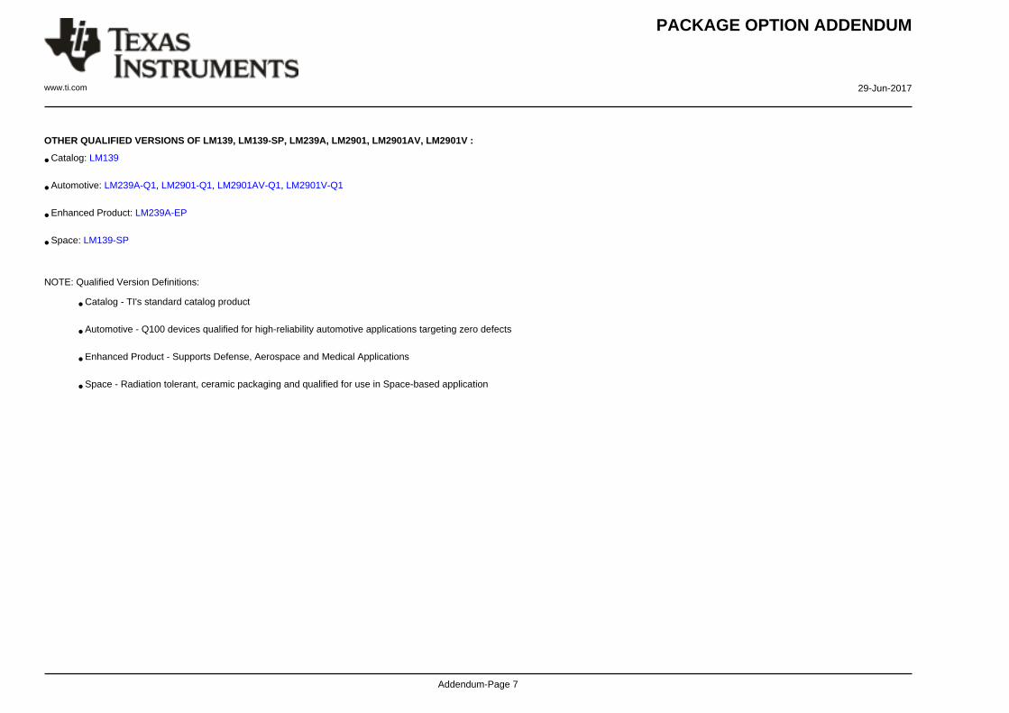
OTHER QUALIFIED VERSIONS OF LM139, LM139-SP, LM239A, LM2901, LM2901AV, LM2901V :
• Catalog: LM139
• Automotive: LM239A-Q1, LM2901-Q1, LM2901AV-Q1, LM2901V-Q1
• Enhanced Product: LM239A-EP
• Space: LM139-SP
NOTE: Qualified Version Definitions:
• Catalog - TI's standard catalog product
• Automotive - Q100 devices qualified for high-reliability automotive applications targeting zero defects
• Enhanced Product - Supports Defense, Aerospace and Medical Applications
• Space - Radiation tolerant, ceramic packaging and qualified for use in Space-based application
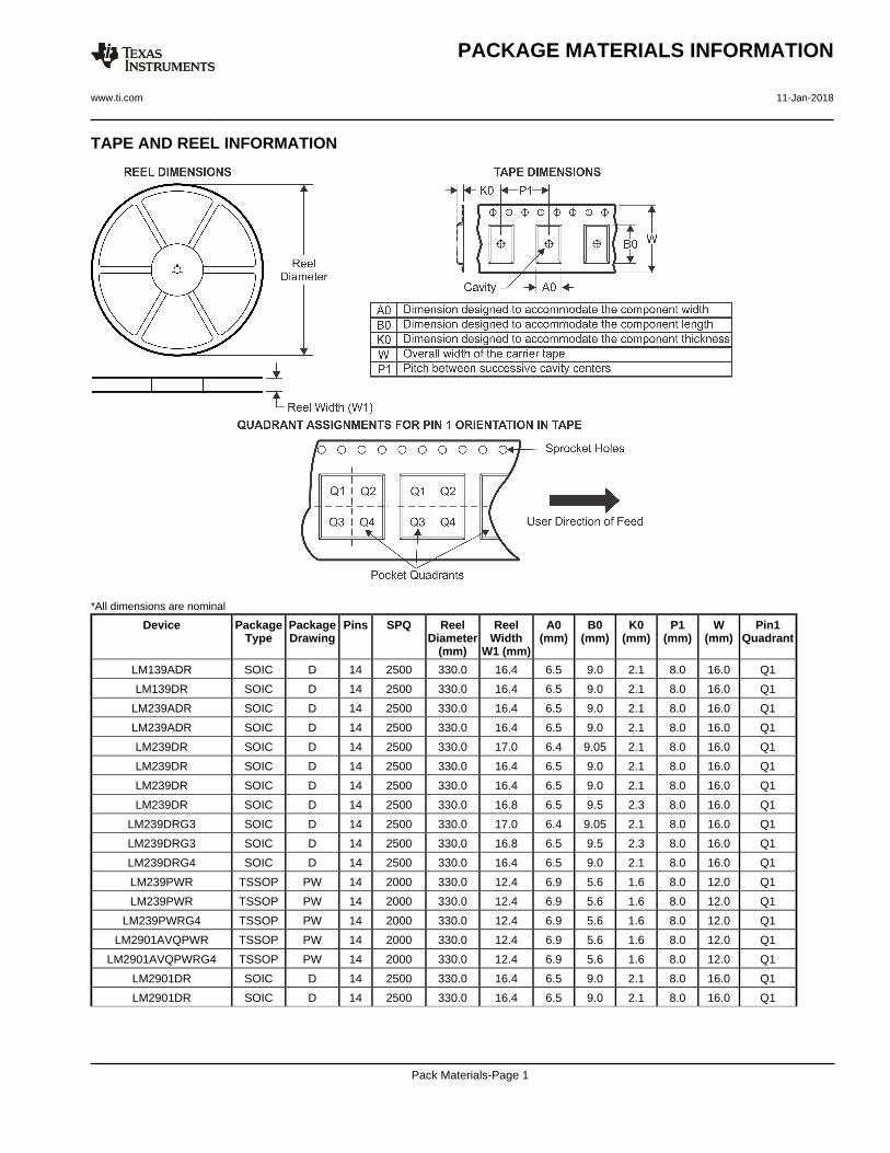
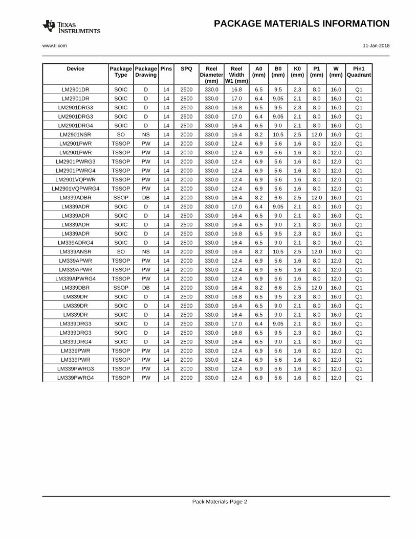
TAPE AND REEL INFORMATION
*All dimensions are nominal
Device PackageType
PackageDrawing
Pins SPQ ReelDiameter
(mm)
ReelWidth
W1 (mm)
A0(mm)
B0(mm)
K0(mm)
P1(mm)
W(mm)
Pin1Quadrant
LM139ADR SOIC D 14 2500 330.0 16.4 6.5 9.0 2.1 8.0 16.0 Q1
LM139DR SOIC D 14 2500 330.0 16.4 6.5 9.0 2.1 8.0 16.0 Q1
LM239ADR SOIC D 14 2500 330.0 16.4 6.5 9.0 2.1 8.0 16.0 Q1
LM239ADR SOIC D 14 2500 330.0 16.4 6.5 9.0 2.1 8.0 16.0 Q1
LM239DR SOIC D 14 2500 330.0 17.0 6.4 9.05 2.1 8.0 16.0 Q1
LM239DR SOIC D 14 2500 330.0 16.4 6.5 9.0 2.1 8.0 16.0 Q1
LM239DR SOIC D 14 2500 330.0 16.4 6.5 9.0 2.1 8.0 16.0 Q1
LM239DR SOIC D 14 2500 330.0 16.8 6.5 9.5 2.3 8.0 16.0 Q1
LM239DRG3 SOIC D 14 2500 330.0 17.0 6.4 9.05 2.1 8.0 16.0 Q1
LM239DRG3 SOIC D 14 2500 330.0 16.8 6.5 9.5 2.3 8.0 16.0 Q1
LM239DRG4 SOIC D 14 2500 330.0 16.4 6.5 9.0 2.1 8.0 16.0 Q1
LM239PWR TSSOP PW 14 2000 330.0 12.4 6.9 5.6 1.6 8.0 12.0 Q1
LM239PWR TSSOP PW 14 2000 330.0 12.4 6.9 5.6 1.6 8.0 12.0 Q1
LM239PWRG4 TSSOP PW 14 2000 330.0 12.4 6.9 5.6 1.6 8.0 12.0 Q1
LM2901AVQPWR TSSOP PW 14 2000 330.0 12.4 6.9 5.6 1.6 8.0 12.0 Q1
LM2901AVQPWRG4 TSSOP PW 14 2000 330.0 12.4 6.9 5.6 1.6 8.0 12.0 Q1
LM2901DR SOIC D 14 2500 330.0 16.4 6.5 9.0 2.1 8.0 16.0 Q1
LM2901DR SOIC D 14 2500 330.0 16.4 6.5 9.0 2.1 8.0 16.0 Q1
PACKAGE MATERIALS INFORMATION
www.ti.com 11-Jan-2018
Pack Materials-Page 1
Device PackageType
PackageDrawing
Pins SPQ ReelDiameter
(mm)
ReelWidth
W1 (mm)
A0(mm)
B0(mm)
K0(mm)
P1(mm)
W(mm)
Pin1Quadrant
LM2901DR SOIC D 14 2500 330.0 16.8 6.5 9.5 2.3 8.0 16.0 Q1
LM2901DR SOIC D 14 2500 330.0 17.0 6.4 9.05 2.1 8.0 16.0 Q1
LM2901DRG3 SOIC D 14 2500 330.0 16.8 6.5 9.5 2.3 8.0 16.0 Q1
LM2901DRG3 SOIC D 14 2500 330.0 17.0 6.4 9.05 2.1 8.0 16.0 Q1
LM2901DRG4 SOIC D 14 2500 330.0 16.4 6.5 9.0 2.1 8.0 16.0 Q1
LM2901NSR SO NS 14 2000 330.0 16.4 8.2 10.5 2.5 12.0 16.0 Q1
LM2901PWR TSSOP PW 14 2000 330.0 12.4 6.9 5.6 1.6 8.0 12.0 Q1
LM2901PWR TSSOP PW 14 2000 330.0 12.4 6.9 5.6 1.6 8.0 12.0 Q1
LM2901PWRG3 TSSOP PW 14 2000 330.0 12.4 6.9 5.6 1.6 8.0 12.0 Q1
LM2901PWRG4 TSSOP PW 14 2000 330.0 12.4 6.9 5.6 1.6 8.0 12.0 Q1
LM2901VQPWR TSSOP PW 14 2000 330.0 12.4 6.9 5.6 1.6 8.0 12.0 Q1
LM2901VQPWRG4 TSSOP PW 14 2000 330.0 12.4 6.9 5.6 1.6 8.0 12.0 Q1
LM339ADBR SSOP DB 14 2000 330.0 16.4 8.2 6.6 2.5 12.0 16.0 Q1
LM339ADR SOIC D 14 2500 330.0 17.0 6.4 9.05 2.1 8.0 16.0 Q1
LM339ADR SOIC D 14 2500 330.0 16.4 6.5 9.0 2.1 8.0 16.0 Q1
LM339ADR SOIC D 14 2500 330.0 16.4 6.5 9.0 2.1 8.0 16.0 Q1
LM339ADR SOIC D 14 2500 330.0 16.8 6.5 9.5 2.3 8.0 16.0 Q1
LM339ADRG4 SOIC D 14 2500 330.0 16.4 6.5 9.0 2.1 8.0 16.0 Q1
LM339ANSR SO NS 14 2000 330.0 16.4 8.2 10.5 2.5 12.0 16.0 Q1
LM339APWR TSSOP PW 14 2000 330.0 12.4 6.9 5.6 1.6 8.0 12.0 Q1
LM339APWR TSSOP PW 14 2000 330.0 12.4 6.9 5.6 1.6 8.0 12.0 Q1
LM339APWRG4 TSSOP PW 14 2000 330.0 12.4 6.9 5.6 1.6 8.0 12.0 Q1
LM339DBR SSOP DB 14 2000 330.0 16.4 8.2 6.6 2.5 12.0 16.0 Q1
LM339DR SOIC D 14 2500 330.0 16.8 6.5 9.5 2.3 8.0 16.0 Q1
LM339DR SOIC D 14 2500 330.0 16.4 6.5 9.0 2.1 8.0 16.0 Q1
LM339DR SOIC D 14 2500 330.0 16.4 6.5 9.0 2.1 8.0 16.0 Q1
LM339DRG3 SOIC D 14 2500 330.0 17.0 6.4 9.05 2.1 8.0 16.0 Q1
LM339DRG3 SOIC D 14 2500 330.0 16.8 6.5 9.5 2.3 8.0 16.0 Q1
LM339DRG4 SOIC D 14 2500 330.0 16.4 6.5 9.0 2.1 8.0 16.0 Q1
LM339PWR TSSOP PW 14 2000 330.0 12.4 6.9 5.6 1.6 8.0 12.0 Q1
LM339PWR TSSOP PW 14 2000 330.0 12.4 6.9 5.6 1.6 8.0 12.0 Q1
LM339PWRG3 TSSOP PW 14 2000 330.0 12.4 6.9 5.6 1.6 8.0 12.0 Q1
LM339PWRG4 TSSOP PW 14 2000 330.0 12.4 6.9 5.6 1.6 8.0 12.0 Q1
PACKAGE MATERIALS INFORMATION
www.ti.com 11-Jan-2018
Pack Materials-Page 2
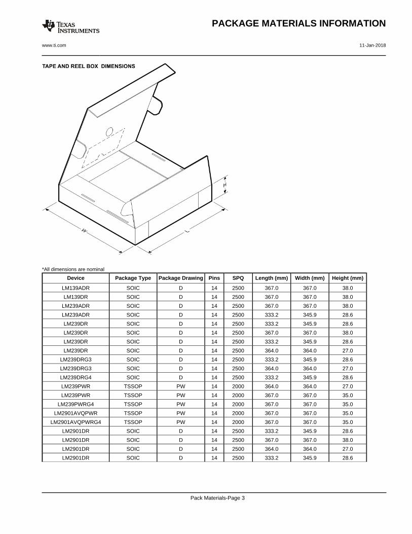
*All dimensions are nominal
Device Package Type Package Drawing Pins SPQ Length (mm) Width (mm) Height (mm)
LM139ADR SOIC D 14 2500 367.0 367.0 38.0
LM139DR SOIC D 14 2500 367.0 367.0 38.0
LM239ADR SOIC D 14 2500 367.0 367.0 38.0
LM239ADR SOIC D 14 2500 333.2 345.9 28.6
LM239DR SOIC D 14 2500 333.2 345.9 28.6
LM239DR SOIC D 14 2500 367.0 367.0 38.0
LM239DR SOIC D 14 2500 333.2 345.9 28.6
LM239DR SOIC D 14 2500 364.0 364.0 27.0
LM239DRG3 SOIC D 14 2500 333.2 345.9 28.6
LM239DRG3 SOIC D 14 2500 364.0 364.0 27.0
LM239DRG4 SOIC D 14 2500 333.2 345.9 28.6
LM239PWR TSSOP PW 14 2000 364.0 364.0 27.0
LM239PWR TSSOP PW 14 2000 367.0 367.0 35.0
LM239PWRG4 TSSOP PW 14 2000 367.0 367.0 35.0
LM2901AVQPWR TSSOP PW 14 2000 367.0 367.0 35.0
LM2901AVQPWRG4 TSSOP PW 14 2000 367.0 367.0 35.0
LM2901DR SOIC D 14 2500 333.2 345.9 28.6
LM2901DR SOIC D 14 2500 367.0 367.0 38.0
LM2901DR SOIC D 14 2500 364.0 364.0 27.0
LM2901DR SOIC D 14 2500 333.2 345.9 28.6
PACKAGE MATERIALS INFORMATION
www.ti.com 11-Jan-2018
Pack Materials-Page 3
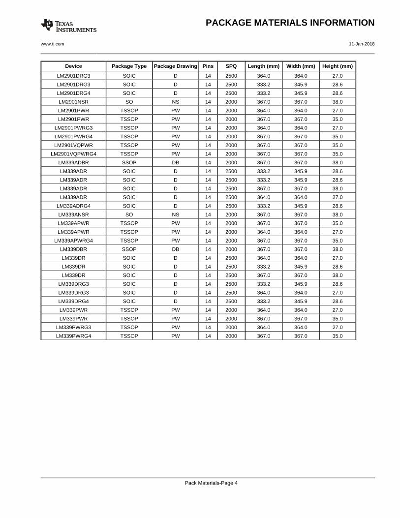
Device Package Type Package Drawing Pins SPQ Length (mm) Width (mm) Height (mm)
LM2901DRG3 SOIC D 14 2500 364.0 364.0 27.0
LM2901DRG3 SOIC D 14 2500 333.2 345.9 28.6
LM2901DRG4 SOIC D 14 2500 333.2 345.9 28.6
LM2901NSR SO NS 14 2000 367.0 367.0 38.0
LM2901PWR TSSOP PW 14 2000 364.0 364.0 27.0
LM2901PWR TSSOP PW 14 2000 367.0 367.0 35.0
LM2901PWRG3 TSSOP PW 14 2000 364.0 364.0 27.0
LM2901PWRG4 TSSOP PW 14 2000 367.0 367.0 35.0
LM2901VQPWR TSSOP PW 14 2000 367.0 367.0 35.0
LM2901VQPWRG4 TSSOP PW 14 2000 367.0 367.0 35.0
LM339ADBR SSOP DB 14 2000 367.0 367.0 38.0
LM339ADR SOIC D 14 2500 333.2 345.9 28.6
LM339ADR SOIC D 14 2500 333.2 345.9 28.6
LM339ADR SOIC D 14 2500 367.0 367.0 38.0
LM339ADR SOIC D 14 2500 364.0 364.0 27.0
LM339ADRG4 SOIC D 14 2500 333.2 345.9 28.6
LM339ANSR SO NS 14 2000 367.0 367.0 38.0
LM339APWR TSSOP PW 14 2000 367.0 367.0 35.0
LM339APWR TSSOP PW 14 2000 364.0 364.0 27.0
LM339APWRG4 TSSOP PW 14 2000 367.0 367.0 35.0
LM339DBR SSOP DB 14 2000 367.0 367.0 38.0
LM339DR SOIC D 14 2500 364.0 364.0 27.0
LM339DR SOIC D 14 2500 333.2 345.9 28.6
LM339DR SOIC D 14 2500 367.0 367.0 38.0
LM339DRG3 SOIC D 14 2500 333.2 345.9 28.6
LM339DRG3 SOIC D 14 2500 364.0 364.0 27.0
LM339DRG4 SOIC D 14 2500 333.2 345.9 28.6
LM339PWR TSSOP PW 14 2000 364.0 364.0 27.0
LM339PWR TSSOP PW 14 2000 367.0 367.0 35.0
LM339PWRG3 TSSOP PW 14 2000 364.0 364.0 27.0
LM339PWRG4 TSSOP PW 14 2000 367.0 367.0 35.0
PACKAGE MATERIALS INFORMATION
www.ti.com 11-Jan-2018
Pack Materials-Page 4
www.ti.com
PACKAGE OUTLINE
C
14X .008-.014 [0.2-0.36]TYP
-150
AT GAGE PLANE
-.314.308-7.977.83[ ]
14X -.026.014-0.660.36[ ]14X -.065.045
-1.651.15[ ]
.2 MAX TYP[5.08]
.13 MIN TYP[3.3]
TYP-.060.015-1.520.38[ ]
4X .005 MIN[0.13]
12X .100[2.54]
.015 GAGE PLANE[0.38]
A
-.785.754-19.9419.15[ ]
B -.283.245-7.196.22[ ]
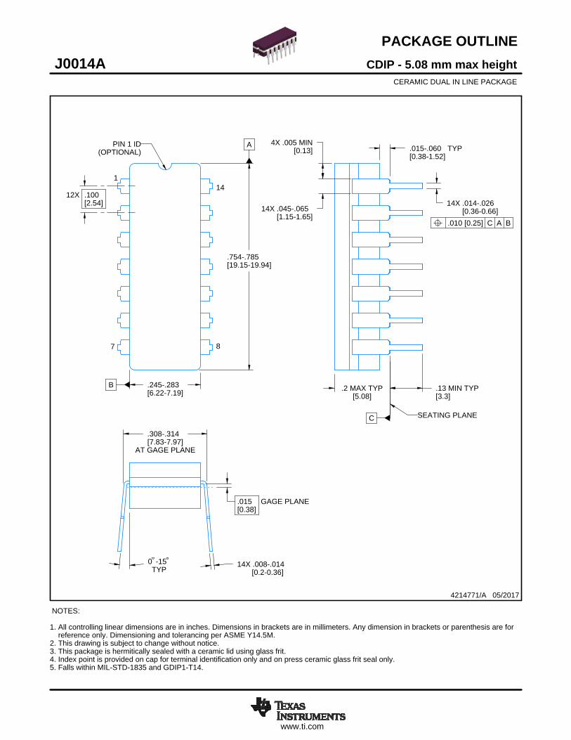
CDIP - 5.08 mm max heightJ0014ACERAMIC DUAL IN LINE PACKAGE
4214771/A 05/2017
NOTES: 1. All controlling linear dimensions are in inches. Dimensions in brackets are in millimeters. Any dimension in brackets or parenthesis are for reference only. Dimensioning and tolerancing per ASME Y14.5M.2. This drawing is subject to change without notice. 3. This package is hermitically sealed with a ceramic lid using glass frit.4. Index point is provided on cap for terminal identification only and on press ceramic glass frit seal only.5. Falls within MIL-STD-1835 and GDIP1-T14.
7 8
141
PIN 1 ID(OPTIONAL)
SCALE 0.900
SEATING PLANE
.010 [0.25] C A B
www.ti.com
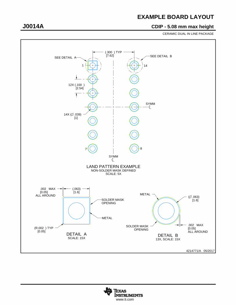
EXAMPLE BOARD LAYOUT
ALL AROUND[0.05]
MAX.002
.002 MAX[0.05]ALL AROUND
SOLDER MASKOPENING
METAL
(.063)[1.6]
(R.002 ) TYP[0.05]
14X ( .039)[1]
( .063)[1.6]
12X (.100 )[2.54]
(.300 ) TYP[7.62]
CDIP - 5.08 mm max heightJ0014ACERAMIC DUAL IN LINE PACKAGE
4214771/A 05/2017
LAND PATTERN EXAMPLENON-SOLDER MASK DEFINED
SCALE: 5X
SEE DETAIL A SEE DETAIL B
SYMM
SYMM
1
7 8
14
DETAIL ASCALE: 15X
SOLDER MASKOPENING
METAL
DETAIL B13X, SCALE: 15X
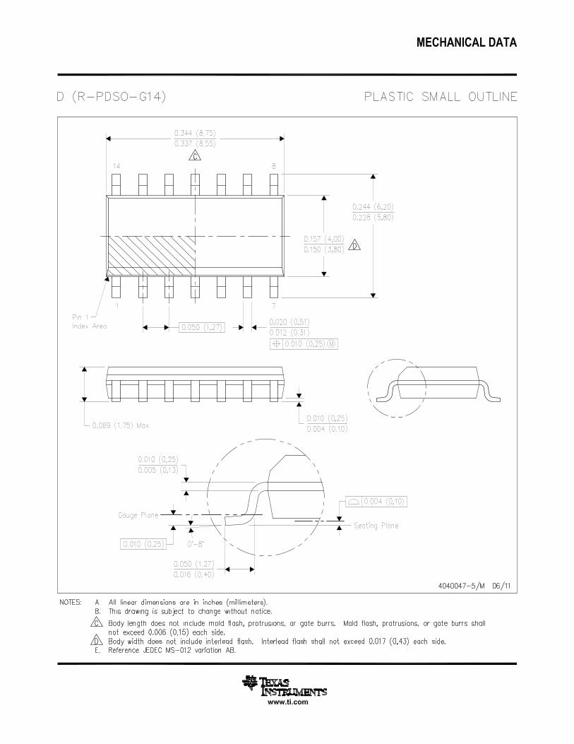

MECHANICAL DATA
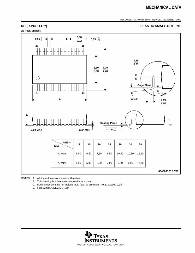
MSSO002E – JANUARY 1995 – REVISED DECEMBER 2001
POST OFFICE BOX 655303 • DALLAS, TEXAS 75265
DB (R-PDSO-G**) PLASTIC SMALL-OUTLINE
4040065 /E 12/01
28 PINS SHOWN
Gage Plane
8,207,40
0,550,95
0,25
38
12,90
12,30
28
10,50
24
8,50
Seating Plane
9,907,90
30
10,50
9,90
0,38
5,605,00
15
0,22
14
A
28
1
2016
6,506,50
14
0,05 MIN
5,905,90
DIM
A MAX
A MIN
PINS **
2,00 MAX
6,90
7,50
0,65 M0,15
0°–8°
0,10
0,090,25
NOTES: A. All linear dimensions are in millimeters.B. This drawing is subject to change without notice.C. Body dimensions do not include mold flash or protrusion not to exceed 0,15.D. Falls within JEDEC MO-150
IMPORTANT NOTICE
Texas Instruments Incorporated (TI) reserves the right to make corrections, enhancements, improvements and other changes to itssemiconductor products and services per JESD46, latest issue, and to discontinue any product or service per JESD48, latest issue. Buyersshould obtain the latest relevant information before placing orders and should verify that such information is current and complete.TI’s published terms of sale for semiconductor products (http://www.ti.com/sc/docs/stdterms.htm) apply to the sale of packaged integratedcircuit products that TI has qualified and released to market. Additional terms may apply to the use or sale of other types of TI products andservices.Reproduction of significant portions of TI information in TI data sheets is permissible only if reproduction is without alteration and isaccompanied by all associated warranties, conditions, limitations, and notices. TI is not responsible or liable for such reproduceddocumentation. Information of third parties may be subject to additional restrictions. Resale of TI products or services with statementsdifferent from or beyond the parameters stated by TI for that product or service voids all express and any implied warranties for theassociated TI product or service and is an unfair and deceptive business practice. TI is not responsible or liable for any such statements.Buyers and others who are developing systems that incorporate TI products (collectively, “Designers”) understand and agree that Designersremain responsible for using their independent analysis, evaluation and judgment in designing their applications and that Designers havefull and exclusive responsibility to assure the safety of Designers' applications and compliance of their applications (and of all TI productsused in or for Designers’ applications) with all applicable regulations, laws and other applicable requirements. Designer represents that, withrespect to their applications, Designer has all the necessary expertise to create and implement safeguards that (1) anticipate dangerousconsequences of failures, (2) monitor failures and their consequences, and (3) lessen the likelihood of failures that might cause harm andtake appropriate actions. Designer agrees that prior to using or distributing any applications that include TI products, Designer willthoroughly test such applications and the functionality of such TI products as used in such applications.TI’s provision of technical, application or other design advice, quality characterization, reliability data or other services or information,including, but not limited to, reference designs and materials relating to evaluation modules, (collectively, “TI Resources”) are intended toassist designers who are developing applications that incorporate TI products; by downloading, accessing or using TI Resources in anyway, Designer (individually or, if Designer is acting on behalf of a company, Designer’s company) agrees to use any particular TI Resourcesolely for this purpose and subject to the terms of this Notice.TI’s provision of TI Resources does not expand or otherwise alter TI’s applicable published warranties or warranty disclaimers for TIproducts, and no additional obligations or liabilities arise from TI providing such TI Resources. TI reserves the right to make corrections,enhancements, improvements and other changes to its TI Resources. TI has not conducted any testing other than that specificallydescribed in the published documentation for a particular TI Resource.Designer is authorized to use, copy and modify any individual TI Resource only in connection with the development of applications thatinclude the TI product(s) identified in such TI Resource. NO OTHER LICENSE, EXPRESS OR IMPLIED, BY ESTOPPEL OR OTHERWISETO ANY OTHER TI INTELLECTUAL PROPERTY RIGHT, AND NO LICENSE TO ANY TECHNOLOGY OR INTELLECTUAL PROPERTYRIGHT OF TI OR ANY THIRD PARTY IS GRANTED HEREIN, including but not limited to any patent right, copyright, mask work right, orother intellectual property right relating to any combination, machine, or process in which TI products or services are used. Informationregarding or referencing third-party products or services does not constitute a license to use such products or services, or a warranty orendorsement thereof. Use of TI Resources may require a license from a third party under the patents or other intellectual property of thethird party, or a license from TI under the patents or other intellectual property of TI.TI RESOURCES ARE PROVIDED “AS IS” AND WITH ALL FAULTS. TI DISCLAIMS ALL OTHER WARRANTIES ORREPRESENTATIONS, EXPRESS OR IMPLIED, REGARDING RESOURCES OR USE THEREOF, INCLUDING BUT NOT LIMITED TOACCURACY OR COMPLETENESS, TITLE, ANY EPIDEMIC FAILURE WARRANTY AND ANY IMPLIED WARRANTIES OFMERCHANTABILITY, FITNESS FOR A PARTICULAR PURPOSE, AND NON-INFRINGEMENT OF ANY THIRD PARTY INTELLECTUALPROPERTY RIGHTS. TI SHALL NOT BE LIABLE FOR AND SHALL NOT DEFEND OR INDEMNIFY DESIGNER AGAINST ANY CLAIM,INCLUDING BUT NOT LIMITED TO ANY INFRINGEMENT CLAIM THAT RELATES TO OR IS BASED ON ANY COMBINATION OFPRODUCTS EVEN IF DESCRIBED IN TI RESOURCES OR OTHERWISE. IN NO EVENT SHALL TI BE LIABLE FOR ANY ACTUAL,DIRECT, SPECIAL, COLLATERAL, INDIRECT, PUNITIVE, INCIDENTAL, CONSEQUENTIAL OR EXEMPLARY DAMAGES INCONNECTION WITH OR ARISING OUT OF TI RESOURCES OR USE THEREOF, AND REGARDLESS OF WHETHER TI HAS BEENADVISED OF THE POSSIBILITY OF SUCH DAMAGES.Unless TI has explicitly designated an individual product as meeting the requirements of a particular industry standard (e.g., ISO/TS 16949and ISO 26262), TI is not responsible for any failure to meet such industry standard requirements.Where TI specifically promotes products as facilitating functional safety or as compliant with industry functional safety standards, suchproducts are intended to help enable customers to design and create their own applications that meet applicable functional safety standardsand requirements. Using products in an application does not by itself establish any safety features in the application. Designers mustensure compliance with safety-related requirements and standards applicable to their applications. Designer may not use any TI products inlife-critical medical equipment unless authorized officers of the parties have executed a special contract specifically governing such use.Life-critical medical equipment is medical equipment where failure of such equipment would cause serious bodily injury or death (e.g., lifesupport, pacemakers, defibrillators, heart pumps, neurostimulators, and implantables). Such equipment includes, without limitation, allmedical devices identified by the U.S. Food and Drug Administration as Class III devices and equivalent classifications outside the U.S.TI may expressly designate certain products as completing a particular qualification (e.g., Q100, Military Grade, or Enhanced Product).Designers agree that it has the necessary expertise to select the product with the appropriate qualification designation for their applicationsand that proper product selection is at Designers’ own risk. Designers are solely responsible for compliance with all legal and regulatoryrequirements in connection with such selection.Designer will fully indemnify TI and its representatives against any damages, costs, losses, and/or liabilities arising out of Designer’s non-compliance with the terms and provisions of this Notice.
Mailing Address: Texas Instruments, Post Office Box 655303, Dallas, Texas 75265Copyright © 2018, Texas Instruments Incorporated


![Finale 2005 - [CAVALGADA] · PDF fileroberto carlos arr. manoel ferreira & & & & & & & & & & & & & &?????](https://img.pdfslide.net/doc/110x75/5a72754e7f8b9a9d538d9075/finale-2005-cavalgadawww2secultcegovbrrecursospublicwebbancopdf.jpg)