Embed Size (px)
Citation preview
8/6/2019 Lnct Letter
http://slidepdf.com/reader/full/lnct-letter 1/6
Abstract — This paper describes on how to formulate a spacevector modulator for the two-level inverter topology typicallyused for Low power induction motor drives. Space vector Pulse
Width Modulation variable speed drives are increasingly appliedin Many new industrial applications that require superiorperformance. In this Scheme V/Hz (Scalar control) ratiomaintain constant in order to get constant Torque over the entireoperating range. In such scheme A constant voltage andfrequency (V/Hz) supply to a.c drives is invariably obtained froma three-phase two level voltage source inverter. There is an
increasing trend of using space vector PWM (SVPWM) because
of their easier digital realization and better dc bus utilization.
The model of a three-phase voltage source inverter is discussedbased on space vector theory. Simulation results are obtainedusing PSIM Software with a 45-KW (60 Hp) motor drive. Testresult are given for effectiveness of the study .
Index Terms — Two Level Inverter, space vector modulation(SVM), Scalar control (Constant V/Hz)
I. INTRODUCTION
HE TWO-Level inverter topology has attracted attention in
high power medium voltage drive applications. Fig. 1
shows Main circuit of Three phase voltage source
inverter.Single-phase VSI cover low-range power applications
and three-phase VSI cover the medium- to high-power
applications[1]. The Main purpose of these topologies is to
provide a three-phase voltage source, where the amplitude,
phase, and frequency of the voltages should always be
controllable. Although most of the applications require
sinusoidal voltage waveforms (e.g., ASDs, UPSs, FACTS,
VAR compensators), arbitrary voltages are also required insome emerging applications (e.g., active filters, voltage
compensators)[2]. The standard three-phase VSI topology is
shown in Fig. 1 it has = 8 eight switching states and aregiven in Table 1[3]. The switches of any leg of the inverter
(S1 and S4, S3 and S6, or S5 and S2) cannot be switched on
simultaneously because this would result in a short circuitacross the dc link voltage supply. Similarly, in order to avoid
undefined states in the VSI, and thus undefined ac output
line voltages, the switches of any leg of the inverter cannot be
switched off simultaneously as this will result in voltages that
will depend upon the respective line current polarity. Out of
the eight switching states, two of them (7 and 8 in Table 1)produce zero ac line voltages[2].
TABLE 1
SWITCHING VECTORS, PHASE VOLTAGES AND LINE VOLTAGES
In this case, the ac line currents freewheel through either theupper or lower components[9]. The remaining states (1 to 6 in
Table 1) produce non-zero ac output voltages. In order to
generate a given voltage waveform, the inverter moves from
one state to another. Thus the resulting ac output line voltages
consist of discrete values of voltages that are Vi , 0, and -Vifor the topology shown in Fig. 1. The selection of the states inorder to generate the given waveform is done by the
modulating technique that should ensure the use of only the
valid states[2]
II. TWO - LEVEL INVERTER SCHEME FOR AN
INDUCTION MOTOR DRIVE
The circuit model of a typical three-phase voltage source
PWM inverter is shown in Fig. 1 There are the six power
switches(IGBT) that shape the output, which are controlled bythe switching variables a, a‟, b, b‟, c and c‟[4]. When an upper
IGBT is switched on, i.e., when a, b or c is 1,the
corresponding lower IGBT is switched off, i.e .,thecorresponding a‟, b‟ or c‟ is 0.Therefore, the on and off states
of the upper IGBT S1, S3 and S5 can be used to determine theoutput voltage[5].The relationship between the switching
variable vector [a, b, c]t and the line-to-line voltage Vector[Vab Vbc Vca]t is given by (2.1) in the following:[5][6]
Simulation Of SVPWM Method For Two Level
Inverter Fed Induction Motor Drive
Manish G Prajapati1,Rohit D Prajapati
2and Prof. Pinkal J Patel
3
E-Mail Id :- [email protected], [email protected] and [email protected]
3Assis. Professor, Dept of Electrical Engineering, S.P.C.E,Visnagar, Gujarat, India
1 & 2 Student,Dept. of Electrical Engineering, S.P.C.E, Visnagar, Gujarat, India
Voltage
Vector
Switching
Vector
Line to Neutral
Voltage
Line to Line
Voltage
a b c Van Vbn Vcn Vab Vbc Vca
V0 0 0 0 0 0 0 0 0 0
V1 1 0 0 2/3 -1/3 -1/3 1 0 -1
V2 1 1 0 1/3 1/3 -2/3 0 1 -1
V3 0 1 0 -1/3 2/3 -1/3 -1 1 0
V4 0 1 1 -2/3 1/3 1/3 -1 0 1
V5 0 0 1 -1/3 -1/3 2/3 0 -1 1
V6 1 0 1 1/3 -2/3 1/3 1 -1 0
V7 1 1 1 0 0 0 0 0 0
8/6/2019 Lnct Letter
http://slidepdf.com/reader/full/lnct-letter 2/6
Fig. 1. Three-phase voltage source PWM Inverter
= Vdc (2.1)
Also, the relationship between the switching variable vector
[a, b, c]t and the phase voltage Vector [Va Vb Vc]t can be
expressed below[5][6].
=3
Vdc(2.2)
As illustrated in Fig. 1, there are eight possible
combinations of on and off patterns for the three upper power
switches[6]. The on and off states of the lower power devices
are opposite to the upper one and so are easily determined
once the states of the upper IGBT are determined[2].
According to equations (2.1) and (2.2), the eight switching
vectors, output line to neutral voltage (phase voltage), andoutput line-to-line voltages in terms of DC-link Vdc, are
given in Table 1 [5]. Space Vector PWM (SVPWM) refers to
a special switching sequence of the upper three power igbt of a three-phase inverter [6]. It has been shown to generate
less harmonic distortion in the output voltages and orcurrents applied to the phases of an AC motor and to provide
more efficient use of supply voltage compared with sinusoidal
modulation technique [4]. Fig 2 Show the basic Switching
Vector of SVPWM Technique. In this schemes there are eightvalid switching state out of six active switching space vector
are evenly distributed 60° interval with 2 Vdc/3 length and
form a hexagon also two zero space vector are located at the
center of hexagon in the complex plane as shown in fig 2.[7]For a given Magnitude (length) and position, Vref can be
synthesized by three near by stationary vectors, based on
which the switching states of the inverter can be selected and
gate signals for the active switches can be generated [8]. WhenVref passes through sectors one by one, different sets of
switches will be turned on or off. As a result, when Vref
rotates one revolution in space, the inverter output voltagevaries one cycle over time. The inverter output frequency
corresponds to the rotating speed of Vref, while its output
Fig 2 Basic switching vectors and sectors
voltage can be adjusted by the Magnitude of Vref. „The Vref
(called the reference vector) vector rotates counter clockwise
with the angle θ varying between 0 and 360 degrees.[9]
III. PRINCIPLE OF CONSTANT V/HZ CONTROL
FOR INDUCTION MOTORS
In this type of control, the motor is fed with variable
frequency supply generated by the PWM control of an
inverter[10]. At steady state the machine terminal voltage isgiven by
V = jώA (3.1)
where V and A are the phasors of stator voltage and stator flux,
2ππ
1VVA (3.2)
It follows that if the ratio V/f remains constant with the change
of f , then A also remains constant and the torque is
independent of the supply frequency[3]. So in order to get
constant torque over the entire operating range The V/f ratio is
maintain constant. Since only magnitudes of the input
variables frequency and voltage are controlled, this isknown as “scalar control”[10] In actual implementation the
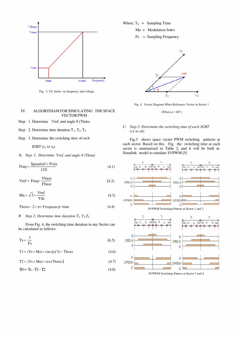
ratio between the Magnitude and frequency of the statorvoltage is usually based on the rated values of these variables,also known as motor ratings.[6] The realistic control limits
that are placed on the applied voltage and frequency are
illustrated in Fig. 3 [4]
A disadvantage of such a control is that the torque
developed is load dependent as it is not controlled directly.
Also, the transient response of such a control is not fast due to
the predefined switching pattern of the Inverter[10].
8/6/2019 Lnct Letter
http://slidepdf.com/reader/full/lnct-letter 3/6
Fig. 3. V/f limits on frequency and voltage.
IV. ALGORITHAM FOR SIMULATING THE SPACE
VECTOR PWM
Step 1. Determine Vref, and angle θ (Theta)
Step 2. Determine time duration T1, T2, T0
Step 3. Determine the switching time of each
IGBT (s1 to s6)
A. Step 1. Determine Vref , and angle θ (Theta)
120
Poleref SpeedFreq (4.1)
Fbase
VbaseFreqVref (4.2)
Vdc
Vref 3Ma (4.3)
timeFrequencyπ2Theta (4.4)
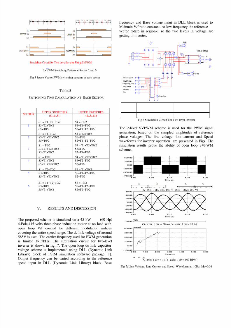
B. Step 2. Determine time duration T 1 , T 2 ,T 0
From Fig. 4, the switching time duration in any Sector can
be calculated as follows:
Fs
1Ts (4.5)
Theta)3pi(sinMa)(TsT1 (4.6)
(Theta)si nMa)(TsT2 ) (4.7)
T2-T1-TsT0 (4.8)
Where, TS = Sampling Time
Ma = Modulation Index
Fs = Sampling Frequency
Fig. 4. Vector Diagram When Reference Vector in Sector 1
(Where α = 60°)
C. Step 3: Determine the switching time of each IGBT
(s1 to s6)
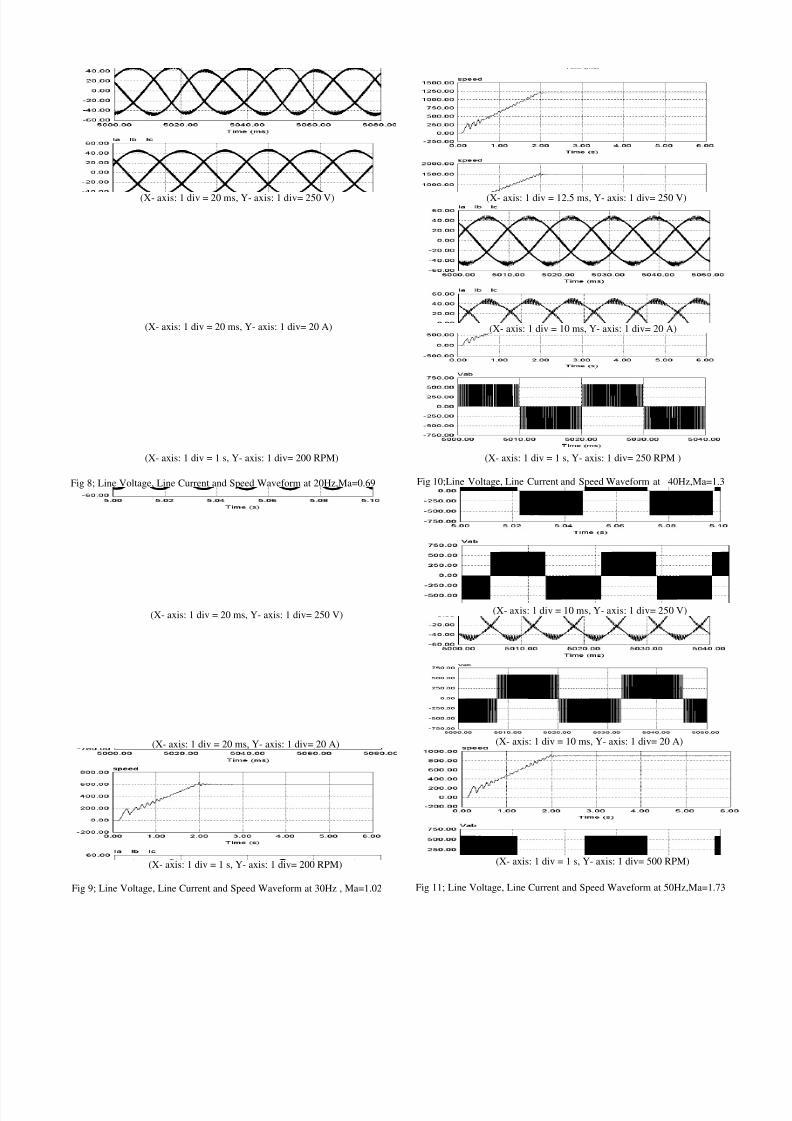
Fig.5 shows space vector PWM switching patterns at
each sector. Based on this Fig. the switching time at each
sector is summarized in Table 2, and it will be built in
Simulink model to simulate SVPWM [5]
SVPWM Switching Pattern at Sector 1 and 2
SVPWM Switching Pattern at Sector 3 and 4
8/6/2019 Lnct Letter
http://slidepdf.com/reader/full/lnct-letter 4/6
SVPWM Switching Pattern at Sector 5 and 6
Fig 5 Space Vector PWM switching patterns at each sector
Table.5
SWITCHING TIME CALCULATION AT EACH SECTOR
SECTOR
UPPER SWITCHES
(S1,S2,S3)
UPPER SWITCHES
(S4,S6,S2)
1
S1 = T1+T2+T0/2
S3=T2+T0/2
S5=T0/2
S4 = T0/2
S6=T1+T0/2
S2=T1+T2+T0/2
2
S1 = T1+T0/2
S3=T1+T2+T0/2
S5=T0/2
S4 = T2+T0/2
S6=T0/2
S2=T1+T2+T0/2
3
S1 = T0/2
S3=T1+T2+T0/2
S5=T2+T0/2
S4 = T1+T2+T0/2
S6=T0/2
S2=T1+T0/2
4
S1 = T0/2
S3=T1+T0/2
S5=T1+T2+T0/2
S4 = T1+T2+T0/2
S6=T2+T0/2
S2=T0/2
5
S1 = T2+T0/2
S3=T0/2S5=T1+T2+T0/2
S4 = T1+T0/2
S6=T1+T2+T0/2S2=T0/2
6
S1 = T1+T2+T0/2
S3=T0/2
S5=T1+T0/2
S4 = T0/2
S6=T1+T2+T0/2
S2=T2+T0/2
V. RESULTS AND DISCUSSION
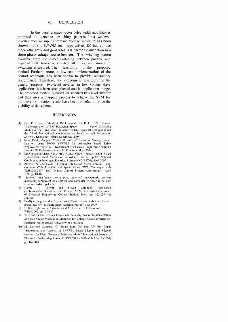
The proposed scheme is simulated on a 45 kW (60 Hp)
4-Pole,415 volts three-phase induction motor at no load with
open loop V/f control for different modulation indicescovering the entire speed range. The dc link voltage of around
585V is used. The carrier frequency used for PWM generationis limited to 5kHz. The simulation circuit for two-level
inverter is shown in fig. 7. The open loop dc link capacitor
voltage scheme is implemented using DLL (Dynamic Link
Library) block of PSIM simulation software package [1].
Output frequency can be varied according to the reference
speed input in DLL (Dynamic Link Library) block. Base
frequency and Base voltage input in DLL block is used to
Maintain V/f ratio constant. At low frequency the reference
vector rotate in region-1 so the two levels in voltage are
getting in inverter.
Fig 6 Simulation Circuit For Two level Inverter
The 2-level SVPWM scheme is used for the PWM signal
generation, based on the sampled amplitudes of reference
phase voltages. The line voltage, line current and Speed
waveforms for inverter operation are presented in Figs. Thesimulation results prove the ability of open loop SVPWM
scheme.
(X- axis: 1 div = 50 ms, Y- axis: 1 div= 250 V)
(X- axis: 1 div = 50 ms, Y- axis: 1 div= 20 A)
(X- axis: 1 div = 1s, Y- axis: 1 div= 100 RPM)
Fig 7; Line Voltage, Line Current and Speed Waveform at 10Hz, Ma=0.34
8/6/2019 Lnct Letter
http://slidepdf.com/reader/full/lnct-letter 5/6
(X- axis: 1 div = 20 ms, Y- axis: 1 div= 250 V)
(X- axis: 1 div = 20 ms, Y- axis: 1 div= 20 A)
(X- axis: 1 div = 1 s, Y- axis: 1 div= 200 RPM)
Fig 8; Line Voltage, Line Current and Speed Waveform at 20Hz,Ma=0.69
(X- axis: 1 div = 20 ms, Y- axis: 1 div= 250 V)
(X- axis: 1 div = 20 ms, Y- axis: 1 div= 20 A)
(X- axis: 1 div = 1 s, Y- axis: 1 div= 200 RPM)
Fig 9; Line Voltage, Line Current and Speed Waveform at 30Hz , Ma=1.02
(X- axis: 1 div = 12.5 ms, Y- axis: 1 div= 250 V)
(X- axis: 1 div = 10 ms, Y- axis: 1 div= 20 A)
(X- axis: 1 div = 1 s, Y- axis: 1 div= 250 RPM )
Fig 10;Line Voltage, Line Current and Speed Waveform at 40Hz,Ma=1.3
(X- axis: 1 div = 10 ms, Y- axis: 1 div= 250 V)
(X- axis: 1 div = 10 ms, Y- axis: 1 div= 20 A)
(X- axis: 1 div = 1 s, Y- axis: 1 div= 500 RPM)
Fig 11; Line Voltage, Line Current and Speed Waveform at 50Hz,Ma=1.73
8/6/2019 Lnct Letter
http://slidepdf.com/reader/full/lnct-letter 6/6
VI. CONCLUSION
In this paper a space vector pulse width modulator is
proposed to generate switching patterns for a two-level
inverter from an input command voltage vector. It has been
shown that the SVPWM technique utilizes DC bus voltage
more efficiently and generates less harmonic distortion in a
three-phase voltage-source inverter. The switching patternavailable from the direct switching between positive andnegative half buses is violated all times and minimum
switching is assured. The feasibility of the proposed
method Further more, a low-cost implementation of thecontrol technique has been shown to provide satisfactory
performance. Therefore, the economical feasibility of thegeneral purpose two-level inverter in low voltage drive
applications has been strengthened and its application range.
The proposed method is based on standard two level inverter
and then uses a mapping process to achieve the SVM for
multilevel. Simulation results have been provided to prove the
viability of the scheme.
REFERENCES
[1] Prof P J Patel, Rakesh A Patel, Vinod Patel,Prof. P. N. Tekwani
“Implementation of Self Balancing Space Vector Switching
Modulator for Three-Level Inverter”, IEEE Region 10 Colloquium and
the Third International Conference on Industrial and Information
Systems, Kharagpur, INDIA December, 2008
[2] Sunil Panda, Anupam Mishra, B Srinivas“Control of Voltage Source
Inverters using PWM/ SVPWM for Adjustable Speed Drive
Applications” thesis of Department of Electrical Engineering National
Institute Of Technology Rourkela, Rourkela ,May- 2009
[3] Mr.Venkatara Mana Naik, Mrs. K.Sree Gowri “Space Vector Based
Hybrid Pulse Width Modulation for reduced Current Ripple” National
Conference on Intelligent Electrical Systems (NCIES‟09), April 2009
[4] Zhenyu Yu and David FigoliAC “Induction Motor Control UsingConstant V/Hz Principle and Space Vector PWM Technique with
TMS320C240” DSP Digital Control System Applications, April
1998,pp 10-18.
[5] jin-woo jung “space vector pwm inverter” mechatronic systems
laboratory department of electrical and computer engineering he ohio
state university, pp 4 - 14.
[6] Hamid A. Toliyat and Steven Campbell “dsp-based
electromechanical motion control”Texas A&M University Department
of Electrical Engineering College Station, Texas, pp 223,224 (v/f
control)
[7] Do-Hyun jang and duck yong yoon “Space vector technique for two
phase inverter fed single phase induction Motor “IEEE 1999
[8] B. Wu, High-Power Converters and AC Drives, IEEE Press and
Wiley,2006, pp 101-117.
[9] Krisztina Leban, Cristian Lascu, and Alin Argeseanu “Implementation
of Space Vector Modulation Strategies for Voltage Source Inverters for
Induction Motor Drives” University of Timisoara
[10] M. Lakshmi Swarupa, G. Tulasi Ram Das and P.V Raj Gopal
“Simulation and Analysis of SVPWM Based 2-Level and 3-Level
Inverters for Direct Torque of Induction Motor” International Journal of
Electronic Engineering Research ISSN 0975 - 6450 Vol- 1 No.3 (2009)
pp. 169 – 184


![FHYY]¸.e]hk ]NYP;[]¸-lNCt ¸;[D;¸FHYYH¸5PiPkH¸H¸ Pkk;FHYY;€¦ · 0YkPZH¸[Hri 5PFH]-;x;HYH¸.eHh;[w][¸O;¸P[D][kh;k]¸;YDl[P¸;ZPDP¸eHh NYP¸;lNlhP ¸ - ¸ ]NYP;[]¸-lNCt](https://img.pdfslide.net/doc/110x75/60dd65242c0b615a0667b045/fhyyehk-nyp-lnct-dfhyyh5pipkhh-pkkfhyy-0ykpzhhri-5pfh-xhyhehhwopdkhkydlpzpdpehh.jpg)


![Macroeconomic Theory - Princeton Universityassets.press.princeton.edu/releases/wickens_questions.pdf2 where the objective is to maximize Vt= s=0 βs[lnct+s+ϕlnlt+s] and where yt is](https://img.pdfslide.net/doc/110x75/5f83f298de01b711432dbbd1/macroeconomic-theory-princeton-2-where-the-objective-is-to-maximize-vt-s0-slnctslnlts.jpg)