Embed Size (px)
Citation preview
http://dx.doi.org/10.5573/JSTS.2014.14.3.300 JOURNAL OF SEMICONDUCTOR TECHNOLOGY AND SCIENCE, VOL.14, NO.3, JUNE, 2014
Manuscript received Nov. 25, 2013; accepted Apr. 5, 2014
Department of Electrical Engineering, KAIST, Daejeon, Korea
E-mail : [email protected]
Load-Balance-Independent High Efficiency Single-
Inductor Multiple-Output (SIMO) DC-DC Converters
Younghun Ko, Yeongshin Jang, Sok-Kyun Han, and Sang-Gug Lee
Abstract—A single-inductor multiple-output (SIMO)
DC-DC converter providing buck and boost outputs
with a new switching sequence is presented. In the
proposed switching sequence, which does not require
any additional blocks, input energy is delivered to
outputs continuously by flowing current through the
inductor, which leads to high conversion efficiency
regardless of the balance between the buck and boost
output loads. Furthermore, instead of multiple output
loop compensation, only the freewheeling current
feedback loop is compensated, which minimizes the
number of off-chip components and nullifies the need
for the equivalent series resistance (ESR) of the
output capacitor for loop compensation. Therefore,
power conversion efficiency and output voltage
ripples can be improved and minimized, respectively.
Implemented in a 0.35- m CMOS, the proposed
SIMO DC-DC converter achieves high conversion
efficiency regardless of the load balance between the
two outputs with maximum efficiency reaching up to
82% under heavy loads.
Index Terms—Single-inductor multiple-output
(SIMO) DC-DC converter, switching sequence, DC-
DC converter, PMIC
I. INTRODUCTION
Along with the growth of the battery-powered portable
device market, the development of efficient power
management integrated circuits (PMIC) is a popular and
active research area. A DC-DC converter, which is a core
block in PMIC, provides a regulated output voltage from
a linearly discharging battery voltage in portable devices.
In many portable devices which require multiple
regulated output voltages from a single battery,
implementing separate DC-DC converters can be a viable
means of generating multiple output voltages. However,
the separate DC-DC converter approaches lead to
increase in cost and size due to the required multiple off-
chip inductors, which is not desirable in portable devices.
To circumvent this issue, single-inductor multiple-output
(SIMO) DC-DC converters have been proposed, which
require only one inductor in regulating multiple output
voltages [1-6]. With all DC-DC converters, achieving
high conversion efficiency is critically important and
SIMO DC-DC converters are no exception; furthermore,
there are several design issues such as cross regulation,
system stability, etc. Addressing these issues, various
SIMO DC-DC converters [1-6] have been reported,
which can be categorized based on the energizing
methods. The works reported in [1] and [2], which adopt
multiple energizing cycles per switching period,
introduced time-multiplexing control and freewheel
switching in discontinuous conduction mode (DCM) and
pseudo-continuous conduction mode (PCCM),
respectively. They have shown good cross-regulation
performances by the adoption of decoupling time among
multiple outputs. On the other hand, [3-6] reported SIMO
DC-DC converters that adopt single energizing cycle per
switching period, respectively. The former shows greater
accuracy characterized by the smaller output voltage
ripples and faster control loops than the latter. [3-5] have
proposed control schemes, each with its own advantages,
However, the applications of the proposed control
JOURNAL OF SEMICONDUCTOR TECHNOLOGY AND SCIENCE, VOL.14, NO.3, JUNE, 2014 301
schemes are limited due to the difficulties in
implementing buck and boost outputs simultaneously. In
[6], the converter provides both buck and boost outputs
simultaneously with smaller number of power switches
while adopting hysteresis mode, overcoming the stability
problem that arises during unbalanced output loads.
However, implementing the hysteresis mode in [6] not
only requires additional blocks such as a power
comparator and a delta-voltage generator circuits, but it
also degrades the power conversion efficiency. This
paper proposes a new switching sequence to generate
multiple buck and boost outputs without requiring
additional blocks while achieving high conversion
efficiency.
This paper is organized as follows. Section II and III
introduce the newly proposed switching sequence and
peak-current control scheme, respectively. Then, the
design details of a DC-DC converter that adopts the
proposed control sequence are described in Section IV
and the measurement results are given in Section V. The
conclusions are given in Section VI.
II. PRINCIPLE OF THE PROPOSED CONTROL
TOPOLOGY
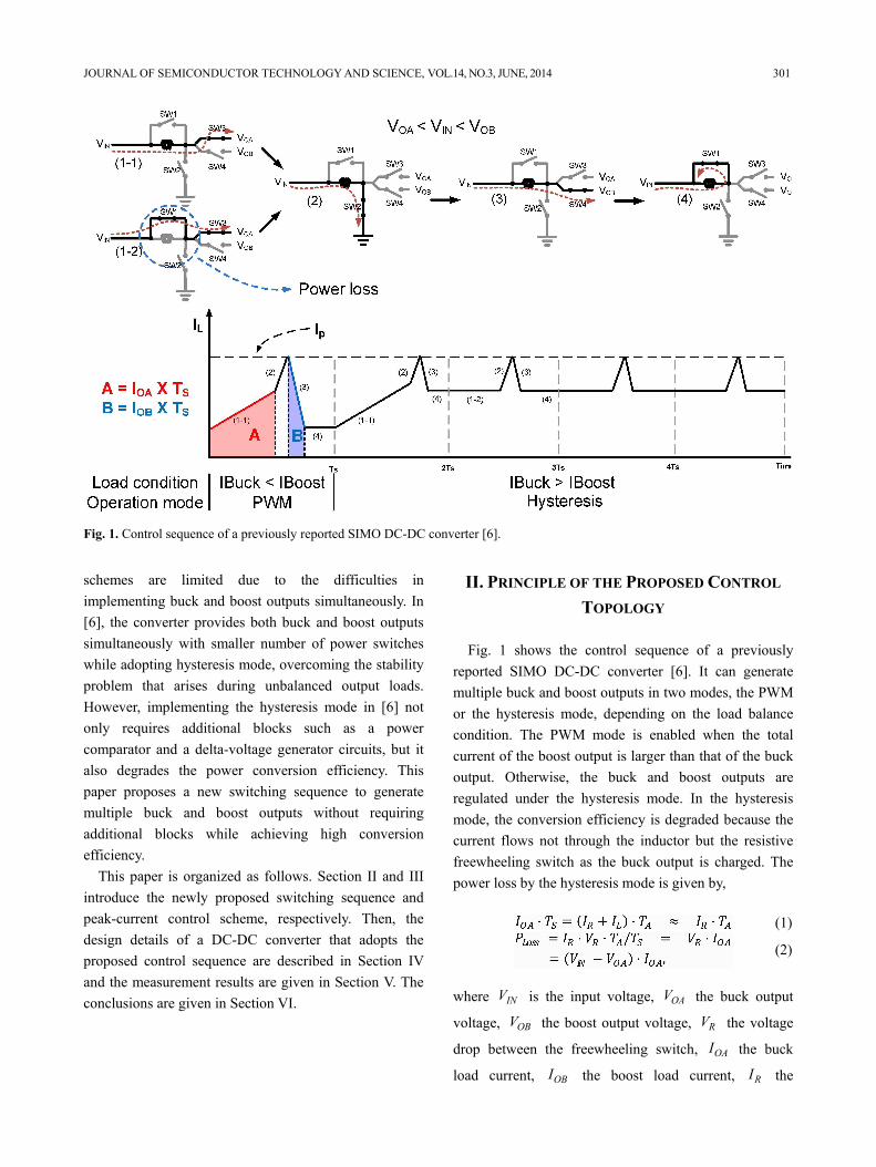
Fig. 1 shows the control sequence of a previously
reported SIMO DC-DC converter [6]. It can generate
multiple buck and boost outputs in two modes, the PWM
or the hysteresis mode, depending on the load balance
condition. The PWM mode is enabled when the total
current of the boost output is larger than that of the buck
output. Otherwise, the buck and boost outputs are
regulated under the hysteresis mode. In the hysteresis
mode, the conversion efficiency is degraded because the
current flows not through the inductor but the resistive
freewheeling switch as the buck output is charged. The
power loss by the hysteresis mode is given by,
(1)
(2)
where INV is the input voltage, OAV the buck output
voltage, OBV the boost output voltage, RV the voltage
drop between the freewheeling switch, OAI the buck
load current, OBI the boost load current, RI the
Fig. 1. Control sequence of a previously reported SIMO DC-DC converter [6].
302 YOUNGHUN KO et al : LOAD-BALANCE-INDEPENDENT HIGH EFFICIENCY SINGLE-INDUCTOR MULTIPLE-OUTPUT (SIMO) …
current through the resistive freewheeling switch, ST
the switching period, AT the time of phase-(1-2) and
LOSSP the power loss during the hysteresis mode. The
conduction loss in the hysteresis mode leads to the drops
in conversion efficiency at the load balance boundary.
Furthermore, to determine the mode of proper operation,
a power comparator and a delta-voltage generator are
required.
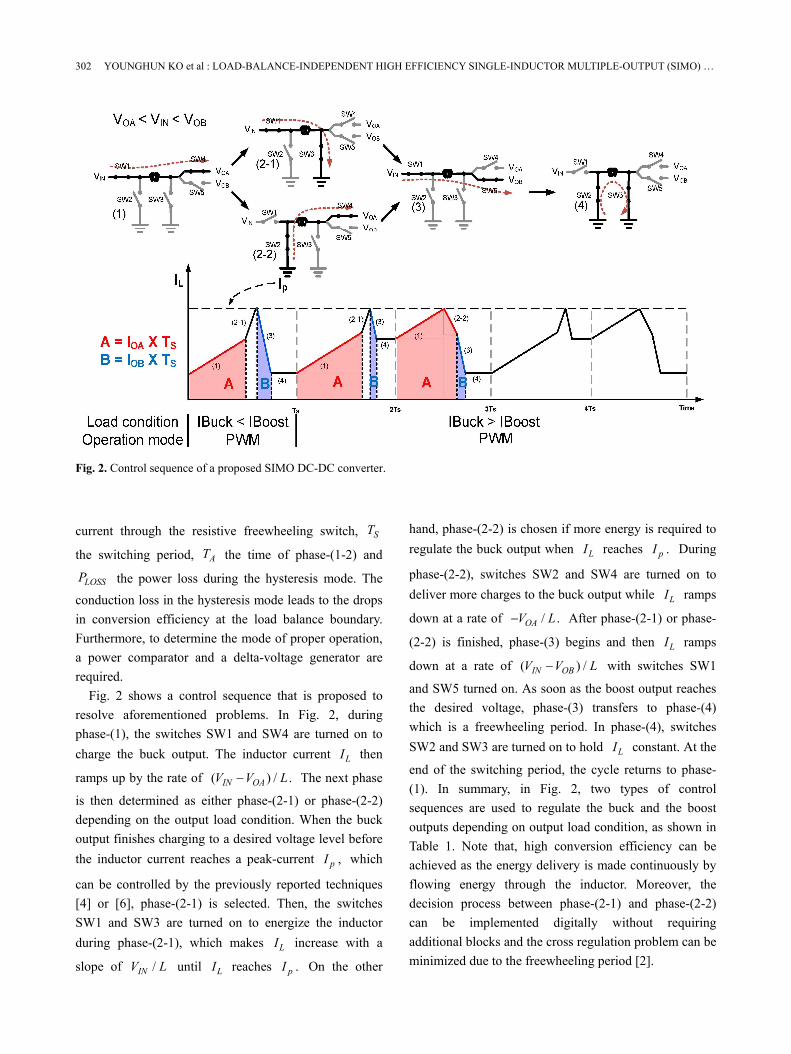
Fig. 2 shows a control sequence that is proposed to
resolve aforementioned problems. In Fig. 2, during
phase-(1), the switches SW1 and SW4 are turned on to
charge the buck output. The inductor current LI then
ramps up by the rate of ( ) / .IN OAV V L− The next phase
is then determined as either phase-(2-1) or phase-(2-2)
depending on the output load condition. When the buck
output finishes charging to a desired voltage level before
the inductor current reaches a peak-current ,pI which
can be controlled by the previously reported techniques
[4] or [6], phase-(2-1) is selected. Then, the switches
SW1 and SW3 are turned on to energize the inductor
during phase-(2-1), which makes LI increase with a
slope of /INV L until LI reaches .pI On the other
hand, phase-(2-2) is chosen if more energy is required to
regulate the buck output when LI reaches .pI During
phase-(2-2), switches SW2 and SW4 are turned on to
deliver more charges to the buck output while LI ramps
down at a rate of / .OAV L− After phase-(2-1) or phase-
(2-2) is finished, phase-(3) begins and then LI ramps
down at a rate of ( ) /IN OBV V L− with switches SW1
and SW5 turned on. As soon as the boost output reaches
the desired voltage, phase-(3) transfers to phase-(4)
which is a freewheeling period. In phase-(4), switches
SW2 and SW3 are turned on to hold LI constant. At the
end of the switching period, the cycle returns to phase-
(1). In summary, in Fig. 2, two types of control
sequences are used to regulate the buck and the boost
outputs depending on output load condition, as shown in
Table 1. Note that, high conversion efficiency can be
achieved as the energy delivery is made continuously by
flowing energy through the inductor. Moreover, the
decision process between phase-(2-1) and phase-(2-2)
can be implemented digitally without requiring
additional blocks and the cross regulation problem can be
minimized due to the freewheeling period [2].
Fig. 2. Control sequence of a proposed SIMO DC-DC converter.
JOURNAL OF SEMICONDUCTOR TECHNOLOGY AND SCIENCE, VOL.14, NO.3, JUNE, 2014 303
III. PEAK-CURRENT CONTROL SCHEME
The peak-current ,pI which is one of the factors that
determines the duty-cycle for each phase, can be
controlled by various schemes such as the load-
dependent peak-current control [6], the freewheeling
current feedback control [4], etc. In order to adopt the
load-dependent peak-current control scheme, all output
voltages including both the buck and boost output should
be sensed by error amplifiers. The error signals between
the output voltages and their reference voltages are used
to control the peak current level. Generally, this scheme
requires off-chip components for a feedback loop
compensation of each output because the required
capacitor values are too large to be integrated. The
number of off-chip components is proportional to the
number of outputs of the SIMO DC-DC converter, which
debases the usefulness of the SIMO DC-DC converter.
On the other hand, in the freewheeling current feedback
control scheme, the output voltages are regulated directly
by comparators. A single compensation is sufficient for a
freewheeling feedback loop. Thus, both cost and chip
area can be reduced simultaneously. Furthermore, the
equivalent series resistance (ESR) of the output capacitor,
which makes a negative zero for loop compensation, is
unnecessary. Therefore, by adopting a capacitor with a
small ESR (ESR of a ceramic capacitor is smaller than
that of a tantal capacitor), not only the output voltage
ripples can be reduced but also the power conversion
efficiency can be improved. Considering aforementioned
advantages, the freewheeling current feedback control
scheme [4] is adopted to implement the SIMO DC-DC
converter with the proposed control sequence. The
concept of the freewheeling current feedback control
scheme is to control the peak current by comparing the
average of the freewheeling current with a reference
current. Due to the differences in control sequence, the
DC and AC characteristics of the proposed SIMO DC-
DC converter are different from those of [4] even though
the same concept of the freewheeling current feedback
control is used. Depending of the load condition, there
are two cases of operational DC and AC characteristics.
Each case is analyzed in the following.
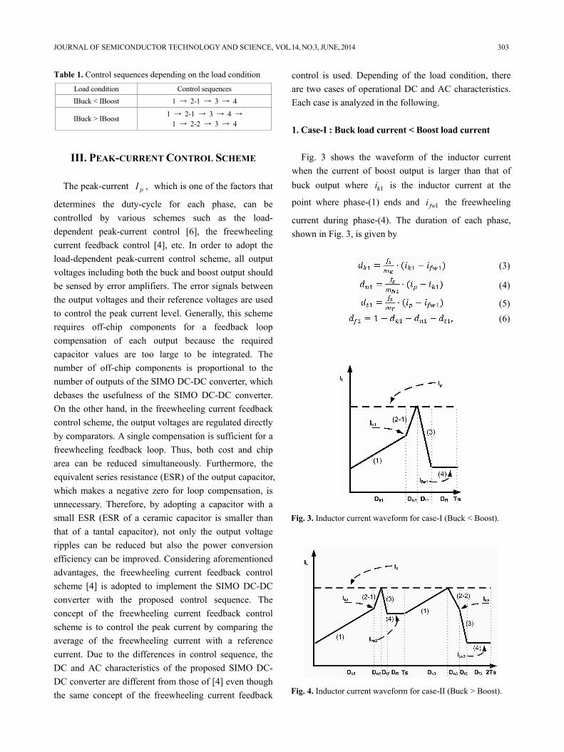
1. Case-I : Buck load current < Boost load current
Fig. 3 shows the waveform of the inductor current
when the current of boost output is larger than that of
buck output where 1ki is the inductor current at the
point where phase-(1) ends and 1fwi the freewheeling
current during phase-(4). The duration of each phase,
shown in Fig. 3, is given by
(3)
(4)
(5)
(6)
Table 1. Control sequences depending on the load condition
Load condition Control sequences
IBuck < IBoost 1 → 2-1 → 3 → 4
IBuck > IBoost 1 → 2-1 → 3 → 4 →
1 → 2-2 → 3 → 4
Fig. 3. Inductor current waveform for case-I (Buck < Boost).
Fig. 4. Inductor current waveform for case-II (Buck > Boost).
304 YOUNGHUN KO et al : LOAD-BALANCE-INDEPENDENT HIGH EFFICIENCY SINGLE-INDUCTOR MULTIPLE-OUTPUT (SIMO) …
where 1, , ,s K Nf m m and Tm are the switching
frequency, ( ) / ,IN OAV V L− / ,INV L and ( ) / ,IN OBV V L− −
respectively. The average value of the freewheeling
current, which should be regulated to the reference
current ( ) ,refI is given by
(7)
(7)
The average value of currents supplied to the buck and
boost outputs are given by
(8)
(9)
From (3)-(9), the DC operating point is determined. At
the given DC operating point, the small signal gain
1( ( ))G s from the perturbation of the peak current ˆ( )pi
to the perturbation of the averaged freewheeling current
1ˆ( )fi can be calculated by constructing perturbation
variable matrices as shown in Table 2. The calculated
1( )G s is used for determining the loop gain of the
freewheeling feedback loop as described in Section IV.
2. Case-II : Buck load current > Boost load current
The inductor current waveform when the current of
boost output is smaller than that of buck output is shown
in Fig. 4 where 2ki is the inductor current at the end of
phase-(1), 3ki the inductor current at the end of phase-
(2-2), 2fwi the freewheeling current during 2 ,fd and
3fwi the freewheeling current during 3 .fd The
duration of each phase is given by
(10)
(11)
(12)
(13)
(14)
(15)
(16)
(17)
where 2Nm is / .OAV L The average freewheeling
current, which should be equal to ,refI is given by
(18)
The average currents supplied to the buck and boost
outputs are given by
(19)
(20)
(21)
(22)
Eqs. (12)-(24) determine the DC operating point. At
the given DC operating point, the small signal gain
2( ( ))G s from ˆpi to the perturbation of the averaged
freewheeling current 2ˆ( )fi can be obtained using
perturbation variable matrices shown in Table 2. The
calculated 2 ( )G s is used for determining the loop gain
of the freewheeling feedback loop as described in
Section IV.
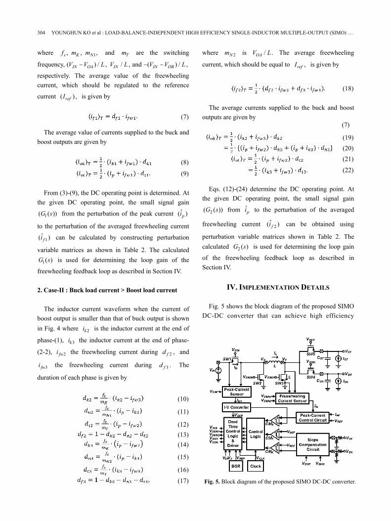
IV. IMPLEMENTATION DETAILS
Fig. 5 shows the block diagram of the proposed SIMO
DC-DC converter that can achieve high efficiency
Fig. 5. Block diagram of the proposed SIMO DC-DC converter.

JOURNAL OF SEMICONDUCTOR TECHNOLOGY AND SCIENCE, VOL.14, NO.3, JUNE, 2014 305
Table 2. Perturbation variable matrices
Case-I : Buck load current < Boost load current
(23)
Case-II : Buck load current > Boost load current
(24)
306 YOUNGHUN KO et al : LOAD-BALANCE-INDEPENDENT HIGH EFFICIENCY SINGLE-INDUCTOR MULTIPLE-OUTPUT (SIMO) …
independent of the load balance. The design parameters
are chosen as 10 H,L µ= 3.7 V,INV = 1.8 V ,OKV =
5 V,OTV = 1 MHz,sf = and 30 mA.refI = The
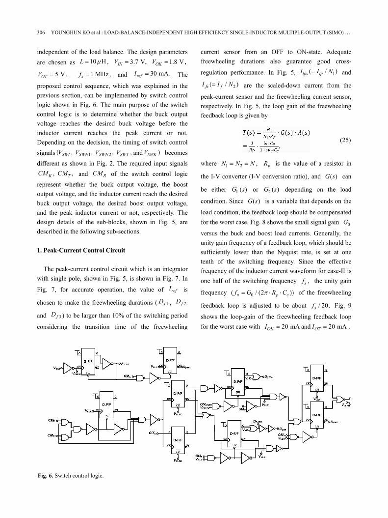
proposed control sequence, which was explained in the
previous section, can be implemented by switch control
logic shown in Fig. 6. The main purpose of the switch
control logic is to determine whether the buck output
voltage reaches the desired buck voltage before the
inductor current reaches the peak current or not.
Depending on the decision, the timing of switch control
signals 1 2( , , , ,SWI SWN SWN SWTV V V V and )SWKV becomes
different as shown in Fig. 2. The required input signals
, ,K TCM CM and RCM of the switch control logic
represent whether the buck output voltage, the boost
output voltage, and the inductor current reach the desired
buck output voltage, the desired boost output voltage,
and the peak inductor current or not, respectively. The
design details of the sub-blocks, shown in Fig. 5, are
described in the following sub-sections.
1. Peak-Current Control Circuit
The peak-current control circuit which is an integrator
with single pole, shown in Fig. 5, is shown in Fig. 7. In
Fig. 7, for accurate operation, the value of refI is
chosen to make the freewheeling durations ( 1fD , 2fD
and 3fD ) to be larger than 10% of the switching period
considering the transition time of the freewheeling
current sensor from an OFF to ON-state. Adequate
freewheeling durations also guarantee good cross-
regulation performance. In Fig. 5, 1( / )lps lpI I N= and
2( / )fs fI I N= are the scaled-down current from the
peak-current sensor and the freewheeling current sensor,
respectively. In Fig. 5, the loop gain of the freewheeling
feedback loop is given by
(25)
where 1 2 ,N N N= = pR is the value of a resistor in
the I-V converter (I-V conversion ratio), and ( )G s can
be either 1 ( )G s or 2 ( )G s depending on the load
condition. Since ( )G s is a variable that depends on the
load condition, the feedback loop should be compensated
for the worst case. Fig. 8 shows the small signal gain 0G
versus the buck and boost load currents. Generally, the
unity gain frequency of a feedback loop, which should be
sufficiently lower than the Nyquist rate, is set at one
tenth of the switching frequency. Since the effective
frequency of the inductor current waveform for case-II is
one half of the switching frequency ,sf the unity gain
frequency 0( / (2 ))u p cf G R Cπ= ⋅ ⋅ of the freewheeling
feedback loop is adjusted to be about / 20.sf Fig. 9
shows the loop-gain of the freewheeling feedback loop
for the worst case with 20 mAOKI = and 20 mAOTI = .
Fig. 6. Switch control logic.
JOURNAL OF SEMICONDUCTOR TECHNOLOGY AND SCIENCE, VOL.14, NO.3, JUNE, 2014 307
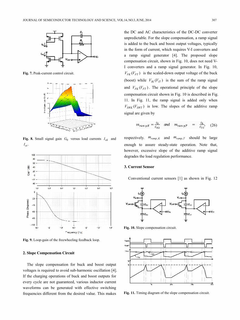
2. Slope Compensation Circuit
The slope compensation for buck and boost output
voltages is required to avoid sub-harmonic oscillation [4].
If the charging operations of buck and boost outputs for
every cycle are not guaranteed, various inductor current
waveforms can be generated with effective switching
frequencies different from the desired value. This makes
the DC and AC characteristics of the DC-DC converter
unpredictable. For the slope compensation, a ramp signal
is added to the buck and boost output voltages, typically
in the form of current, which requires V-I converters and
a ramp signal generator [4]. The proposed slope
compensation circuit, shown in Fig. 10, does not need V-
I converters and a ramp signal generator. In Fig. 10,
( )FK FTV V is the scaled-down output voltage of the buck
(boost) while ( )IK ITV V is the sum of the ramp signal
and ( )FK FTV V . The operational principle of the slope
compensation circuit shown in Fig. 10 is described in Fig.
11. In Fig. 11, the ramp signal is added only when
( )SWK SWTV V is low. The slopes of the additive ramp
signal are given by
(26)
respectively. ,ramp Km and ,ramp Tm should be large
enough to assure steady-state operation. Note that,
however, excessive slope of the additive ramp signal
degrades the load regulation performance.
3. Current Sensor
Conventional current sensors [1] as shown in Fig. 12
Fig. 7. Peak-current control circuit.
Fig. 8. Small signal gain 0G versus load currents okI and
.otI
Fig. 9. Loop-gain of the freewheeling feedback loop.
Fig. 10. Slope compensation circuit.
Fig. 11. Timing diagram of the slope compensation circuit.

308 YOUNGHUN KO et al : LOAD-BALANCE-INDEPENDENT HIGH EFFICIENCY SINGLE-INDUCTOR MULTIPLE-OUTPUT (SIMO) …
are adopted for the peak-current (Fig. 12(a)) and
freewheeling current (Fig. 12(b)) sensors. In Fig. 12, the
current sensors copy the voltage drop across a power
switch into a scale-downed transistor with a scaling ratio
of N. Then, the sensed currents ( lpsI and fsI ), which
has been scale-downed, flow through the scale-downed
transistor.
4. Dead Time Control Logic
In Fig. 5, when more than two power switches are
simultaneously turned on at a given node, a large shoot-
through current can flow, which degrades the conversion
efficiency. Thus, a dead time control logic, which secures
the definite turn - OFF of all other switches when one of
the switches is ON, is designed as the way shown in Fig.
13. In Fig. 13, over and reverse current protection
circuits are also included to protect the DC-DC converter
system and to prevent undesirable power loss. When the
inductor current exceeds the maximum allowed current,
SW1 and SW2 immediately turns OFF and ON,
respectively, for the reduction of the inductor current.
The maximum allowed inductor current is given by
(27)
where N is the current scaling ratio in the current sensor,
OCPR the value of a resistor in the I-V converter (I-V
conversion ratio), and / .OCP L OCPV I R N= ⋅ There are
two reverse current protection cases that can occur,
which can be detected by monitoring the sign of the
voltage drop across SW1 ( )IN XV V− or SW2
( ).XV GND− During the buck operation of case-II
(buck > boost), LI ramps down with SW2 turned ON.
If the charging operation of buck output is not finished
even if LI is reduced to zero, a sign change in the
voltage drop across SW2 promptly turns OFF SW2 to
stop the current loss from the buck output. The current
protection mechanism is similar during the boost
operation as well.
V. MEASUREMENT RESULTS
The proposed SIMO DC-DC converter is implemented
in a 0.35- mµ single poly 4 metal CMOS technology. Fig.
14 shows the chip micrograph of the proposed SIMO DC-
DC converter with a size of 1460 mµ x 1250 mµ
including pads. The proposed SIMO DC-DC converter is
implemented with the following design parameters :
22 F,OK OTC C µ= = 10 H,L µ= 3.7 VINV = ,
1.8 VOKV = , 5 VOTV = , and 1 MHz.sf = Fig. 15
shows the measured output voltage waveforms for the
maximum output load currents showing both buck and
boost output voltages simultaneously. Fig. 16 shows the
measured output voltages and inductor current
waveforms. Fig. 16(a) shows the waveform of the
(a)
(b)
Fig. 12. Schematic of (a) peak-current, (b) freewheeling current
sensors.
Fig. 13. Dead time control logic.

JOURNAL OF SEMICONDUCTOR TECHNOLOGY AND SCIENCE, VOL.14, NO.3, JUNE, 2014 309
inductor current when the boost load current is larger
than the buck load current, while Fig. 16(b) shows for the
other case. The operational mode change, shown in Fig.
16, depending on the output load condition proves that
the output voltages can be regulated without inductor
current accumulation by adopting the proposed control
sequences regardless of the output load conditions. Note
that, the inductor current stays constant ideally during the
freewheeling phase. However, the measured inductor
current decreases considerably during the freewheeling
phase in Fig. 16 due to non-idealities such as the direct
current resistance (DCR) of the inductor and the switch
resistance. This conduction loss could degrade the power
conversion efficiency. Fig. 17 shows the maximum
output ripples for the maximum output load currents. In
Fig. 17, the maximum peak-to-peak output ripples of the
buck and boost outputs are 5.6 and 4.8 mV without spike,
(a)
(b)
Fig. 16. Output voltages and inductor current waveforms for (a)
case-I ( OKI =10 mA and OTI =80 mA), (b) case-II ( OKI =80
mA and OTI =10 mA).
Fig. 17. Maximum output ripples for OKI =80 mA and
OTI =80 mA.
Fig. 14. Micrograph of the proposed SIMO DC-DC converter.
Fig. 15. Output voltage settings.
310 YOUNGHUN KO et al : LOAD-BALANCE-INDEPENDENT HIGH EFFICIENCY SINGLE-INDUCTOR MULTIPLE-OUTPUT (SIMO) …
respectively.
Since the operation of the proposed scheme is stable
even for a small value of ESR, the output voltage ripples
could be minimized. Fig. 18 shows the measured load
transient response for the change in the pulse loads of 10
to 80 mA. The load regulations of the buck and boost
outputs over the load current variations are 10 and 32 mV,
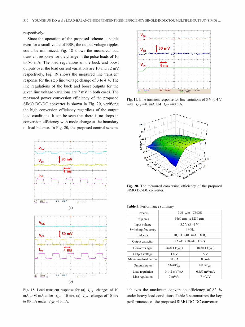
respectively. Fig. 19 shows the measured line transient
response for the step line voltage change of 3 to 4 V. The
line regulations of the buck and boost outputs for the
given line voltage variations are 7 mV in both cases. The
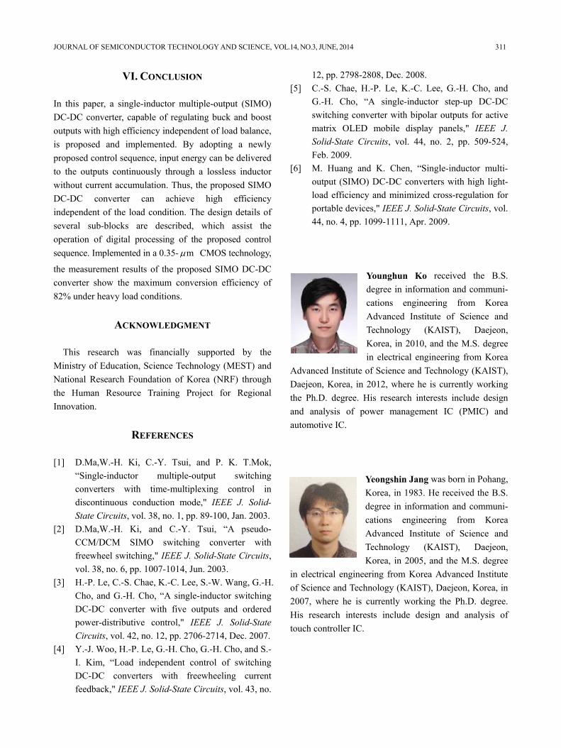
measured power conversion efficiency of the proposed
SIMO DC-DC converter is shown in Fig. 20, verifying
the high conversion efficiency regardless of the output
load conditions. It can be seen that there is no drops in
conversion efficiency with mode change at the boundary
of load balance. In Fig. 20, the proposed control scheme
achieves the maximum conversion efficiency of 82 %
under heavy load conditions. Table 3 summarizes the key
performances of the proposed SIMO DC-DC converter.
Fig. 19. Line transient response for line variations of 3 V to 4 V
with OKI =40 mA and OTI =40 mA.
Fig. 20. The measured conversion efficiency of the proposed
SIMO DC-DC converter.
Table 3. Performance summary
Process 0.35- mµ CMOS
Chip area 1460 mµ x 1250 mµ
Input voltage 3.7 V (3 - 4 V)
Switching frequency 1 MHz
Inductor 10 Hµ (400mΩ DCR)
Output capacitor 22 Fµ (10mΩ ESR)
Converter type Buck ( OKV ) Boost ( OTV )
Output voltage 1.8 V 5 V
Maximum load current 80 mA 80 mA
Output ripples 5.6 ppmV 4.8 ppmV
Load regulation 0.142 mV/mA 0.457 mV/mA
Line regulation 7 mV/V 7 mV/V
(a)
(b)
Fig. 18. Load transient response for (a) OKI changes of 10
mA to 80 mA under OTI =10 mA, (a) OTI changes of 10 mA
to 80 mA under OKI =10 mA.
JOURNAL OF SEMICONDUCTOR TECHNOLOGY AND SCIENCE, VOL.14, NO.3, JUNE, 2014 311
VI. CONCLUSION
In this paper, a single-inductor multiple-output (SIMO)
DC-DC converter, capable of regulating buck and boost
outputs with high efficiency independent of load balance,
is proposed and implemented. By adopting a newly
proposed control sequence, input energy can be delivered
to the outputs continuously through a lossless inductor
without current accumulation. Thus, the proposed SIMO
DC-DC converter can achieve high efficiency
independent of the load condition. The design details of
several sub-blocks are described, which assist the
operation of digital processing of the proposed control
sequence. Implemented in a 0.35- mµ CMOS technology,
the measurement results of the proposed SIMO DC-DC
converter show the maximum conversion efficiency of
82% under heavy load conditions.
ACKNOWLEDGMENT
This research was financially supported by the
Ministry of Education, Science Technology (MEST) and
National Research Foundation of Korea (NRF) through
the Human Resource Training Project for Regional
Innovation.
REFERENCES
[1] D.Ma,W.-H. Ki, C.-Y. Tsui, and P. K. T.Mok,
“Single-inductor multiple-output switching
converters with time-multiplexing control in
discontinuous conduction mode," IEEE J. Solid-
State Circuits, vol. 38, no. 1, pp. 89-100, Jan. 2003.
[2] D.Ma,W.-H. Ki, and C.-Y. Tsui, “A pseudo-
CCM/DCM SIMO switching converter with
freewheel switching," IEEE J. Solid-State Circuits,
vol. 38, no. 6, pp. 1007-1014, Jun. 2003.
[3] H.-P. Le, C.-S. Chae, K.-C. Lee, S.-W. Wang, G.-H.
Cho, and G.-H. Cho, “A single-inductor switching
DC-DC converter with five outputs and ordered
power-distributive control," IEEE J. Solid-State
Circuits, vol. 42, no. 12, pp. 2706-2714, Dec. 2007.
[4] Y.-J. Woo, H.-P. Le, G.-H. Cho, G.-H. Cho, and S.-
I. Kim, “Load independent control of switching
DC-DC converters with freewheeling current
feedback," IEEE J. Solid-State Circuits, vol. 43, no.
12, pp. 2798-2808, Dec. 2008.
[5] C.-S. Chae, H.-P. Le, K.-C. Lee, G.-H. Cho, and
G.-H. Cho, “A single-inductor step-up DC-DC
switching converter with bipolar outputs for active
matrix OLED mobile display panels," IEEE J.
Solid-State Circuits, vol. 44, no. 2, pp. 509-524,
Feb. 2009.
[6] M. Huang and K. Chen, “Single-inductor multi-
output (SIMO) DC-DC converters with high light-
load efficiency and minimized cross-regulation for
portable devices," IEEE J. Solid-State Circuits, vol.
44, no. 4, pp. 1099-1111, Apr. 2009.
Younghun Ko received the B.S.
degree in information and communi-
cations engineering from Korea
Advanced Institute of Science and
Technology (KAIST), Daejeon,
Korea, in 2010, and the M.S. degree
in electrical engineering from Korea
Advanced Institute of Science and Technology (KAIST),
Daejeon, Korea, in 2012, where he is currently working
the Ph.D. degree. His research interests include design
and analysis of power management IC (PMIC) and
automotive IC.
Yeongshin Jang was born in Pohang,
Korea, in 1983. He received the B.S.
degree in information and communi-
cations engineering from Korea
Advanced Institute of Science and
Technology (KAIST), Daejeon,
Korea, in 2005, and the M.S. degree
in electrical engineering from Korea Advanced Institute
of Science and Technology (KAIST), Daejeon, Korea, in
2007, where he is currently working the Ph.D. degree.
His research interests include design and analysis of
touch controller IC.

312 YOUNGHUN KO et al : LOAD-BALANCE-INDEPENDENT HIGH EFFICIENCY SINGLE-INDUCTOR MULTIPLE-OUTPUT (SIMO) …
Sok-Kyun Han received the B.S.
degree in electronics engineering
from Kwangju University, Korea, in
1995, and the M.S. and Ph.D.
degrees in electrical engineering
from Mokpo University and Mokpo
Maritime University, Korea, in 1998
and 2004, respectively. From 1995 to 1998, he was with
Information and Communications University, Daejeon,
Korea, as a research assistant professor. Since 2010, he
has been with the Korea Advanced Institute of Science
and Technology (KAIST), Daejeon, Korea, in the
Department of Electrical Engineering as a Research
Associate Professor. His research interests are the
CMOS-based RFIC and Microwave circuit designs.
Lately, his research interests extend to extreme high-
frequency (THz) circuit designs.
Sang-Gug Lee was born in
Gyungnam, Korea in 1958. He
received the B.S. degree in electronic
engineering from the Gyungbook
National University, Daegue, Korea,
in 1981, and the M.S. and Ph.D.
degrees in electrical engineering
from University of Florida, Gainesville, Florida, in 1989
and 1992, respectively. In 1992, he joined Harris
Semiconductor, Melbourne, Florida, USA, where he was
engaged in silicon-based RF IC designs. From 1995 to
1998, he was with Handong University, Pohang, Korea,
as an assistant professor in the school of computer and
electrical engineering. From 1998 to 2009, he was with
Information and Communications University, Daejeon,
Korea as an assistant, associate, and professor in the
school of engineering. Since March 2009, he is with
KAIST, Daejeon, Korea, as a professor in the department
of electrical engineering. His research interest is the
silicon technology-based (especially in CMOS) radio
transceiver designs, lately focusing on ultra-low power
and extreme high frequencies (that is, Tera Hertz)
implementations. In the past few years, his research
interests also include other analog integrated circuit
designs such as display semiconductors, power
management ICs, and automotive ICs. From 2005 to
2009, he served as a technical committee member of
IEEE ISSCC in the wireless communication technology
committee. From 2005 to 2010, he served as a research
director of Auto-ID Lab Korea. In 2007, his laboratory
was selected as a National Research Laboratory. Since
2012, he is serving as a director of Future Promising
Fusion Technology Pioneer Center, leading a research
group in the area of silicon technology based THz IC
design.