Embed Size (px)
Citation preview
103Journal of Integrated Circuits and Systems 2014; v.9 / n.2:103-109
Local Laser Annealing of Contacts Between MWCNTs and Metallic Electrodes
Jose V. Silveira1, Raluca Savu2, Jacobus W. Swart3, Josue Mendes Filho1, Antonio G. Souza Filho1 and Stanislav A. Moshkalev2
1Departamento de Física, Universidade Federal do Ceará, Fortaleza, 60455-900, Brasil.2Centro de Componentes Semicondutores, Universidade Estadual de Campinas,
Campinas, 13083-870, Brasil.3Faculdade de Engenharia Elétrica e de Computação, Universidade Estadual de Campinas,
Campinas, 13083-852, Brasil, e-mail: [email protected]; [email protected]; [email protected]
ABSTRACT
A new approach to improve the electrical and thermal contacts between multi-walled carbon nanotubes and me-tallic electrodes was developed by using spatially localized laser heating coupled with a micro Raman equipment. After the deposition by dielectrophoresis, the nanotubes were heated in ambient atmosphere by a focused laser beam in order to improve the electrical contacts of the nanostructures with different electrodes (W, Ti and Au) and also to excite the Raman signal of the nanotubes. The changes in the vibrational frequencies of the Raman bands of the nanotubes provides a real time feedback of the treatment conditions allowing to estimate the local tempera-ture, which is used for adjusting the parameters of treatment. Laser treatment tests were performed in a single step (single exposition of the sample to laser) or gradually (successive expositions of the sample to laser, with gradual increase of the used laser power density) and better results were obtained for the gradual treatment tests. Laser treatment of contacts carried out after the calibration of the treatment parameters, showed a reduction of up to three orders of magnitude in the electrical resistance of the devices. The main advantage of this method, when compared with traditional and rapid thermal annealing, is that the thermal treatment is localized in a small region, thus allowing the processing of circuits composed of different materials, whereby each process can be individually controlled.
Index Terms: Nano Devices. Electrical Contact. Local Annealing. Laser Treatment.
I. INTRODUCTION
The use of carbon nanotubes (CNTs) in elec-tronic devices very often requires their integration into electrical circuits. This integration brings a real chal-lenge: the formation of reliable, low-resistance and sta-ble electrical and thermal contacts of the CNTs with metallic electrodes that, due to the very small contact areas, are extremely difficult to achieve [1-4]. A fre-quently used approach to connect nanotubes to pat-terned metal electrodes is based on a controlled deposi-tion by ac dielectrophoresis (DEP) process from liquid dispersions [5-7]. However, the electrical and thermal contacts formed between CNTs deposited by DEP and metallic films are usually poor [7-9] and further pro-cessing is required in order to improve these contacts. For this, conventional (global) thermal treatment or localized annealing is usually employed [10-12].
Low-resistance and stable electrical and ther-mal contacts between CNTs and metallic electrodes are obtained by using conventional high-temperature
annealing in vacuum (875-1175K) [7, 10]. However, if high-temperature processing of samples is not com-patible with other fabrication steps, it is desirable to perform annealing by locally heating the nanotubes and the contact areas without substantial heating of the whole body of the device. Therefore, localized heat treatment of electrical contacts through the use of the Joule effect has also been utilized [11,12].
On the other hand, for local processing of var-ious nanostructures, including carbon nanotubes, laser treatment has been successfully used [13-17]. Experiments regarding nanotubes exposure to laser ra-diation have shown that the high incident laser power density (PD) may cause damages and, consequently, destruction of nanotubes walls. It has been reported that the PD threshold that causes irreversible damage (destruction) of bundles of single wall carbon nano-tubes (SWCNTs) exposed to laser with photon energy of 1.96 eV (wavelength of 632.8 nm) in air is relatively low (10 kW/cm2 for exposures at about 3 minutes and 6 kW/cm2 for exposures at about 3 hours) [13,16].
Local Laser Annealing of Contacts Between MWCNTs and Metallic Electrodes Silveira, Savu, Swart, Mendes Filho, Souza Filho & Moshkalev
104 Journal of Integrated Circuits and Systems 2014; v.9 / n.2:103-109
Laser processing of nanotubes for contacts improvement has been limited to the use of lasers to activation of the field emission effect for metallic or oxide arrays containing immersed nanotubes [18-22]. Lee et al. [18] made use of the laser for obtaining a SWCNTs/silver ink for field emission devices. By laser heating, they exposed the ends of CNTs embedded in a silver ink in order to obtain the field emission effect. After laser exposure, the field threshold required for generating a given current density emission decreased from 4.0 V to 0.6 V. This was attributed to improve-ment of the electrical contact between CNTs and the electrodes.
This work presents a method of treating the electrical and thermal nano-contacts by localized laser heating, applicable to both individual and bundle of nanotubes. The method uses the same laser for local heating treatment and confocal Raman spectroscopy, allowing in situ determination and control (indirectly) of the local temperatures reached by the nanotubes. These temperature measurements were performed by monitoring the frequency shift of the Raman G band for multi-wall carbon nanotubes (MWCNTs) [22] and adjusting the incident laser power density on the sample.
The method presented here has as the main feature the fast local processing of previously selected areas, with high spatial resolution (determined by the spot size of the laser) and laser scanning which can be used to treat larger areas. The main advantage lies in the selection of the areas to be treated. The process can be performed on previously selected small regions (being the smallest side length limited to the spot size diameter of the laser) and allows the processing of complex circuits, each individual contact area can be controlled individually. Therefore, it is possible to treat different areas using different experimental parameters (power density, exposure time, etc.) chosen according to the characteristics of each contact area to be treated and/or of the each device configuration.
II. EXPERIMENTAL PROCEDURE
Metallic electrodes were obtained by depositing 150 nm thick Ti, W or Au thin films by sputtering over thermally oxidized silicon wafers (SiO2 thickness - 500 nm). The p atterning of the electrodes was made by photolithography followed by wet chemical etching. The electrode pairs were fabricated by a focused ion beam (FIB - NOVA 200 Nanolab - FEI Co.), as de-scribed elsewhere [23]. I x V curves were measured in order to confirm the absence of leakage between the so prepared electrodes.
The multi-walled carbon nanotubes (length of 2-5 mm, diameter of 20-30 nm) used in this research
were purchased from CNT Co Ltd., being synthesized by chemical vapor deposition (CVD). Deposition of the nanotubes on metal electrodes was made by ac di-electrophoresis (DEP). Prior to deposition, the nano-structures were suspended in ethanol (concentration of 3 µg/ml) at room temperature using ultrasound. For the DEP deposition, a droplet of suspension of about 3 ml was placed on the central part of the electrode pair. By using an 8116A HP/Agilent wave function gener-ator, a peak-to-peak bias potential from 3 to 10 V, a frequency of 100 kHz were applied to the electrodes for 60 s. This procedure leads to alignment and depo-sition of MWCNTs over electrodes, with their central parts suspended over the gap (5 mm deep) and their ends supported over the metal electrodes [Inset Fig. 1]. After deposition, the samples were washed with de-ionized water and dried with N2.
Laser treatment of the MWCNTs over the elec-trodes was performed in ambient atmosphere, with simultaneous Raman spectra collection (NTEGRA Spectra system, NT-MDT Co.). The system is equipped with an Olympus objective lens (x100) with a numerical aperture of 0.95 (laser spot ~ 600 nm) and with a 473 nm wavelength laser operating in a backscattering geometry. Under laser heating, the temperature of the nanotubes were estimated from the downshift of the G band, using a conversion fac-tor of ∂ω/∂T = -0.028 cm-1/K. This value is the same as the one measured for MWCNTs grown by arc dis-charge method, which was observed to be indepen-dent of the laser energy [22].
Three treatment routes (R#) were tested:a) for the first route (R#1), the laser treat-
ment was performed in a single step, within the single Raman mapping (for each sample) made in continuum
Figure 1. Raman spectra collected on an array of suspended MWCNTs. The inset shows the schematic drawing of the device, with the nanotube sus-pended over the electrodes.
Local Laser Annealing of Contacts Between MWCNTs and Metallic Electrodes Silveira, Savu, Swart, Mendes Filho, Souza Filho & Moshkalev
105Journal of Integrated Circuits and Systems 2014; v.9 / n.2:103-109
scanning mode at preselected regions at a constant val-ue of the laser power density (PD) of 900 kW/cm2 (or 2.7 mW on the sample).
b) during the second route (R#2), gradually increasing laser power density was tested, with the laser spot fixed at the same position during all treat-ment (i.e., not in scanning mode) and the laser PD was gradually increased. For each value of PD used, the corresponding Raman spectrum of the MWCNTs was collected during 40 s. Three series of tests were performed: in the first series (s1u), the measurements of the Raman spectra were made with successive in-creases of the incident laser PD, step by step, from 60 kW/cm2 to 1700 kW/cm2 (laser power on the sample from 0.17 mW to 5.1 mW). In the second one (s1d), measurements of the Raman spectra were made with successive reductions of the incident power density, and, finally, in the third series (s2u) the Raman spec-tra were collected during successive increases of the laser PD.
c) the third route (R#3) consists of a combina-tion of the first (R#1) and second (R#2) routes, i.e. the laser treatment was performed in stages throughout the area of interest. For this proceeding, the selected area for laser treatment of the contacts undergone four laser scans (Raman mapping, as for R#1 route), with gradual increase of the laser PD (as for R#2 route) used for each scan. The laser treatment was applied starting with a DP of 200 kW/cm2 and increasing to 500 kW/cm2, 900 kW/cm2 and 1200 kW/cm2 in sub-sequent scans (Raman intensity maps). After each la-ser scan, high-resolution scanning electron microscopy (HR-SEM - 200 Nanolab of FEI Co.) was used for the structural and morphological analysis of samples. For observing possible changes in the electrical resistance of the samples, I x V curves were also performed using a 2636A source-meter (Keithley Instruments, Inc.), with the applied bias usually varying between -0.5V and 0.5V.
Raman maps (R#1 and R#3 routes) were made in continuum scanning at preselected regions, with the laser focused on the surface of the electrodes. The scanning direction was always chosen along the gap (crossing electrodes), and the step between the scanning lines was 1 mm.
Figure 1 show the Raman spectrum (frequen-cies from 850 cm-1 and 1790 cm-1), measured using a 60 kW/cm2 laser power density (~ 170 µW on the sample) over the suspended part (Inset Fig. 1) of the nanotubes bridging a pair of W electrodes. The D and G Raman bands of the MWCNTs are observed at 1586 cm-1 and 1359 cm-1, respectively. The second order (Si’’) Raman band of silicon, located around 950 cm-1, was also observed due to exposure of the silicon sub-strate by the laser focused over the gap between the electrodes.
III.RESULTS AND DISCUSSION
A. Laser treatment using the R#1 route
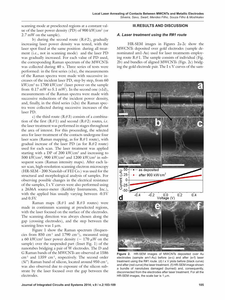
HR-SEM images in Figures 2a-2c show the MWCNTs deposited over gold electrodes (sample de-nominated am1-Au) used for laser treatments employ-ing route R#1. The sample consists of individual (Fig. 2b) and bundles of aligned MWCNTs (Figs. 2c) bridg-ing the gold electrode pair. The I x V curves of the sam-
Figure 2. HR-SEM images of MWCNTs deposited over Au electrodes (sample am1-Au) before (a-c) and after (e-f) laser treatment using the R#1 route. (d) I x V plots before (black curve) and after (red curve) the laser treatment. (f) HR-SEM image shown a bundle of nanotubes damaged (burned) and, consequently, disconnected from the electrodes after laser treatment. For all the HR-SEM images, the scale bar is 1 mm.
Local Laser Annealing of Contacts Between MWCNTs and Metallic Electrodes Silveira, Savu, Swart, Mendes Filho, Souza Filho & Moshkalev
106 Journal of Integrated Circuits and Systems 2014; v.9 / n.2:103-109
ples before (Fig. 2d - black curve) and after (Fig. 2d - red curve) laser treatment show that the electrical resistance of the sample has increased after the treatment process.
HR-SEM images taken after laser processing (Figs. 2e and 2f) show some nanotubes damaged and disconnected from the electrodes. It was also noted that, for some nanotubes (Fig. 2e) the breaking is not complete, meaning that the time needed for forming a good thermal contact with the Au electrodes is com-parable to the time needed to break the nanotubes. For the nanotubes deposited on W electrodes (sam-ple am1-W, results not shown here) and subjected to the same laser treatment route, all the nanotubes were damaged after laser exposure, indicating that the ther-mal contacts treatment is faster for the gold electrode when compared with the W ones. The HR-SEM im-ages presented in Figures 2e and 2f indicate that the nanotubes have suffered overheating and rupture of the graphitic layers. In fact, estimates for the laser treatment initial phase show that overheating of the nanotubes followed by break-up in air at T~1000 K it is possible. Due to the nanoscale roughness of the met-al thin film electrodes, the real contact area between the as deposited nanotubes and the metal is smaller than the nominal contact area (e.g., < 0.1 nominal contact area). Therefore, the purpose of the laser annealing is to increase the area of real contact, by flattening the met-al surface and promoting stronger adhesion between carbon nanostructures and metal surfaces. Low con-tact area implies low adherence between the contacting surfaces (i.e. carbon-metal) with possible deterioration or complete loss of the contact through cycling time
B. Laser treatment using R#2 route
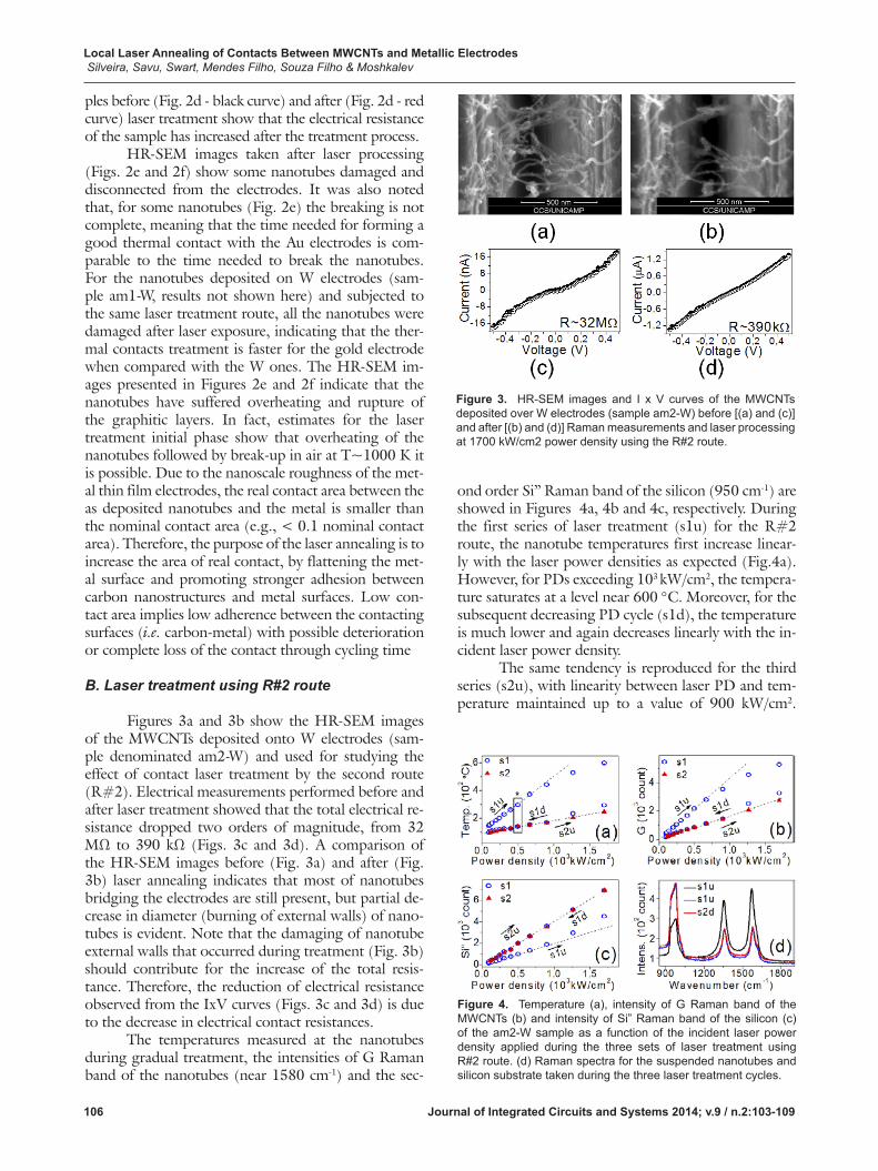
Figures 3a and 3b show the HR-SEM images of the MWCNTs deposited onto W electrodes (sam-ple denominated am2-W) and used for studying the effect of contact laser treatment by the second route (R#2). Electrical measurements performed before and after laser treatment showed that the total electrical re-sistance dropped two orders of magnitude, from 32 MΩ to 390 kΩ (Figs. 3c and 3d). A comparison of the HR-SEM images before (Fig. 3a) and after (Fig. 3b) laser annealing indicates that most of nanotubes bridging the electrodes are still present, but partial de-crease in diameter (burning of external walls) of nano-tubes is evident. Note that the damaging of nanotube external walls that occurred during treatment (Fig. 3b) should contribute for the increase of the total resis-tance. Therefore, the reduction of electrical resistance observed from the IxV curves (Figs. 3c and 3d) is due to the decrease in electrical contact resistances.
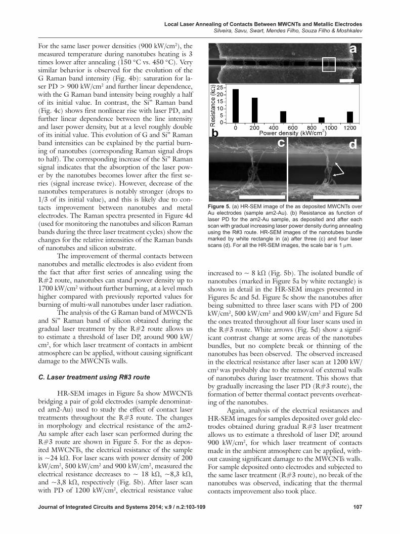
The temperatures measured at the nanotubes during gradual treatment, the intensities of G Raman band of the nanotubes (near 1580 cm-1) and the sec-
ond order Si” Raman band of the silicon (950 cm-1) are showed in Figures 4a, 4b and 4c, respectively. During the first series of laser treatment (s1u) for the R#2 route, the nanotube temperatures first increase linear-ly with the laser power densities as expected (Fig.4a). However, for PDs exceeding 103 kW/cm2, the tempera-ture saturates at a level near 600 °C. Moreover, for the subsequent decreasing PD cycle (s1d), the temperature is much lower and again decreases linearly with the in-cident laser power density.
The same tendency is reproduced for the third series (s2u), with linearity between laser PD and tem-perature maintained up to a value of 900 kW/cm2.
Figure 3. HR-SEM images and I x V curves of the MWCNTs deposited over W electrodes (sample am2-W) before [(a) and (c)] and after [(b) and (d)] Raman measurements and laser processing at 1700 kW/cm2 power density using the R#2 route.
Figure 4. Temperature (a), intensity of G Raman band of the MWCNTs (b) and intensity of Si” Raman band of the silicon (c) of the am2-W sample as a function of the incident laser power density applied during the three sets of laser treatment using R#2 route. (d) Raman spectra for the suspended nanotubes and silicon substrate taken during the three laser treatment cycles.
Local Laser Annealing of Contacts Between MWCNTs and Metallic Electrodes Silveira, Savu, Swart, Mendes Filho, Souza Filho & Moshkalev
107Journal of Integrated Circuits and Systems 2014; v.9 / n.2:103-109
For the same laser power densities (900 kW/cm2), the measured temperature during nanotubes heating is 3 times lower after annealing (150 °C vs. 450 °C). Very similar behavior is observed for the evolution of the G Raman band intensity (Fig. 4b): saturation for la-ser PD > 900 kW/cm2 and further linear dependence, with the G Raman band intensity being roughly a half of its initial value. In contrast, the Si’’ Raman band (Fig. 4c) shows first nonlinear rise with laser PD, and further linear dependence between the line intensity and laser power density, but at a level roughly double of its initial value. This evolution of G and Si” Raman band intensities can be explained by the partial burn-ing of nanotubes (corresponding Raman signal drops to half). The corresponding increase of the Si” Raman signal indicates that the absorption of the laser pow-er by the nanotubes becomes lower after the first se-ries (signal increase twice). However, decrease of the nanotubes temperatures is notably stronger (drops to 1/3 of its initial value), and this is likely due to con-tacts improvement between nanotubes and metal electrodes. The Raman spectra presented in Figure 4d (used for monitoring the nanotubes and silicon Raman bands during the three laser treatment cycles) show the changes for the relative intensities of the Raman bands of nanotubes and silicon substrate.
The improvement of thermal contacts between nanotubes and metallic electrodes is also evident from the fact that after first series of annealing using the R#2 route, nanotubes can stand power density up to 1700 kW/cm2 without further burning, at a level much higher compared with previously reported values for burning of multi-wall nanotubes under laser radiation.
The analysis of the G Raman band of MWCNTs and Si’’ Raman band of silicon obtained during the gradual laser treatment by the R#2 route allows us to estimate a threshold of laser DP, around 900 kW/cm2, for which laser treatment of contacts in ambient atmosphere can be applied, without causing significant damage to the MWCNTs walls.
C. Laser treatment using R#3 route
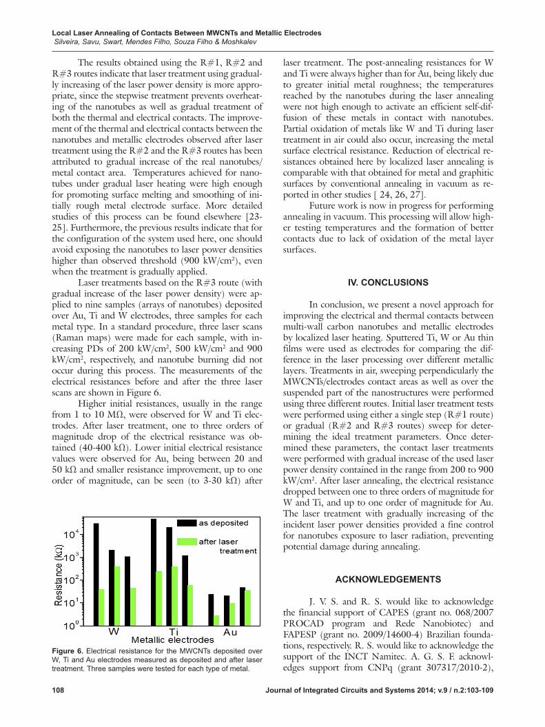
HR-SEM images in Figure 5a show MWCNTs bridging a pair of gold electrodes (sample denominat-ed am2-Au) used to study the effect of contact laser treatments throughout the R#3 route. The changes in morphology and electrical resistance of the am2-Au sample after each laser scan performed during the R#3 route are shown in Figure 5. For the as depos-ited MWCNTs, the electrical resistance of the sample is ~24 kΩ. For laser scans with power density of 200 kW/cm2, 500 kW/cm2 and 900 kW/cm2, measured the electrical resistance decreases to ~ 18 kΩ, ~8,3 kΩ, and ~3,8 kΩ, respectively (Fig. 5b). After laser scan with PD of 1200 kW/cm2, electrical resistance value
increased to ~ 8 kΩ (Fig. 5b). The isolated bundle of nanotubes (marked in Figure 5a by white rectangle) is shown in detail in the HR-SEM images presented in Figures 5c and 5d. Figure 5c show the nanotubes after being submitted to three laser scans with PD of 200 kW/cm2, 500 kW/cm2 and 900 kW/cm2 and Figure 5d the ones treated throughout all four laser scans used in the R#3 route. White arrows (Fig. 5d) show a signif-icant contrast change at some areas of the nanotubes bundles, but no complete break or thinning of the nanotubes has been observed. The observed increased in the electrical resistance after laser scan at 1200 kW/cm2 was probably due to the removal of external walls of nanotubes during laser treatment. This shows that by gradually increasing the laser PD (R#3 route), the formation of better thermal contact prevents overheat-ing of the nanotubes.
Again, analysis of the electrical resistances and HR-SEM images for samples deposited over gold elec-trodes obtained during gradual R#3 laser treatment allows us to estimate a threshold of laser DP, around 900 kW/cm2, for which laser treatment of contacts made in the ambient atmosphere can be applied, with-out causing significant damage to the MWCNTs walls. For sample deposited onto electrodes and subjected to the same laser treatment (R#3 route), no break of the nanotubes was observed, indicating that the thermal contacts improvement also took place.
Figure 5. (a) HR-SEM image of the as deposited MWCNTs over Au electrodes (sample am2-Au). (b) Resistance as function of laser PD for the am2-Au sample, as deposited and after each scan with gradual increasing laser power density during annealing using the R#3 route. HR-SEM images of the nanotubes bundle marked by white rectangle in (a) after three (c) and four laser scans (d). For all the HR-SEM images, the scale bar is 1 mm.
Local Laser Annealing of Contacts Between MWCNTs and Metallic Electrodes Silveira, Savu, Swart, Mendes Filho, Souza Filho & Moshkalev
108 Journal of Integrated Circuits and Systems 2014; v.9 / n.2:103-109
laser treatment. The post-annealing resistances for W and Ti were always higher than for Au, being likely due to greater initial metal roughness; the temperatures reached by the nanotubes during the laser annealing were not high enough to activate an efficient self-dif-fusion of these metals in contact with nanotubes. Partial oxidation of metals like W and Ti during laser treatment in air could also occur, increasing the metal surface electrical resistance. Reduction of electrical re-sistances obtained here by localized laser annealing is comparable with that obtained for metal and graphitic surfaces by conventional annealing in vacuum as re-ported in other studies [ 24, 26, 27].
Future work is now in progress for performing annealing in vacuum. This processing will allow high-er testing temperatures and the formation of better contacts due to lack of oxidation of the metal layer surfaces.
IV. CONCLUSIONS
In conclusion, we present a novel approach for improving the electrical and thermal contacts between multi-wall carbon nanotubes and metallic electrodes by localized laser heating. Sputtered Ti, W or Au thin films were used as electrodes for comparing the dif-ference in the laser processing over different metallic layers. Treatments in air, sweeping perpendicularly the MWCNTs/electrodes contact areas as well as over the suspended part of the nanostructures were performed using three different routes. Initial laser treatment tests were performed using either a single step (R#1 route) or gradual (R#2 and R#3 routes) sweep for deter-mining the ideal treatment parameters. Once deter-mined these parameters, the contact laser treatments were performed with gradual increase of the used laser power density contained in the range from 200 to 900 kW/cm2. After laser annealing, the electrical resistance dropped between one to three orders of magnitude for W and Ti, and up to one order of magnitude for Au. The laser treatment with gradually increasing of the incident laser power densities provided a fine control for nanotubes exposure to laser radiation, preventing potential damage during annealing.
ACKNOWLEDGEMENTS
J. V. S. and R. S. would like to acknowledge the financial support of CAPES (grant no. 068/2007 PROCAD program and Rede Nanobiotec) and FAPESP (grant no. 2009/14600-4) Brazilian founda-tions, respectively. R. S. would like to acknowledge the support of the INCT Namitec. A. G. S. F. acknowl-edges support from CNPq (grant 307317/2010-2),
The results obtained using the R#1, R#2 and R#3 routes indicate that laser treatment using gradual-ly increasing of the laser power density is more appro-priate, since the stepwise treatment prevents overheat-ing of the nanotubes as well as gradual treatment of both the thermal and electrical contacts. The improve-ment of the thermal and electrical contacts between the nanotubes and metallic electrodes observed after laser treatment using the R#2 and the R#3 routes has been attributed to gradual increase of the real nanotubes/metal contact area. Temperatures achieved for nano-tubes under gradual laser heating were high enough for promoting surface melting and smoothing of ini-tially rough metal electrode surface. More detailed studies of this process can be found elsewhere [23-25]. Furthermore, the previous results indicate that for the configuration of the system used here, one should avoid exposing the nanotubes to laser power densities higher than observed threshold (900 kW/cm2), even when the treatment is gradually applied.
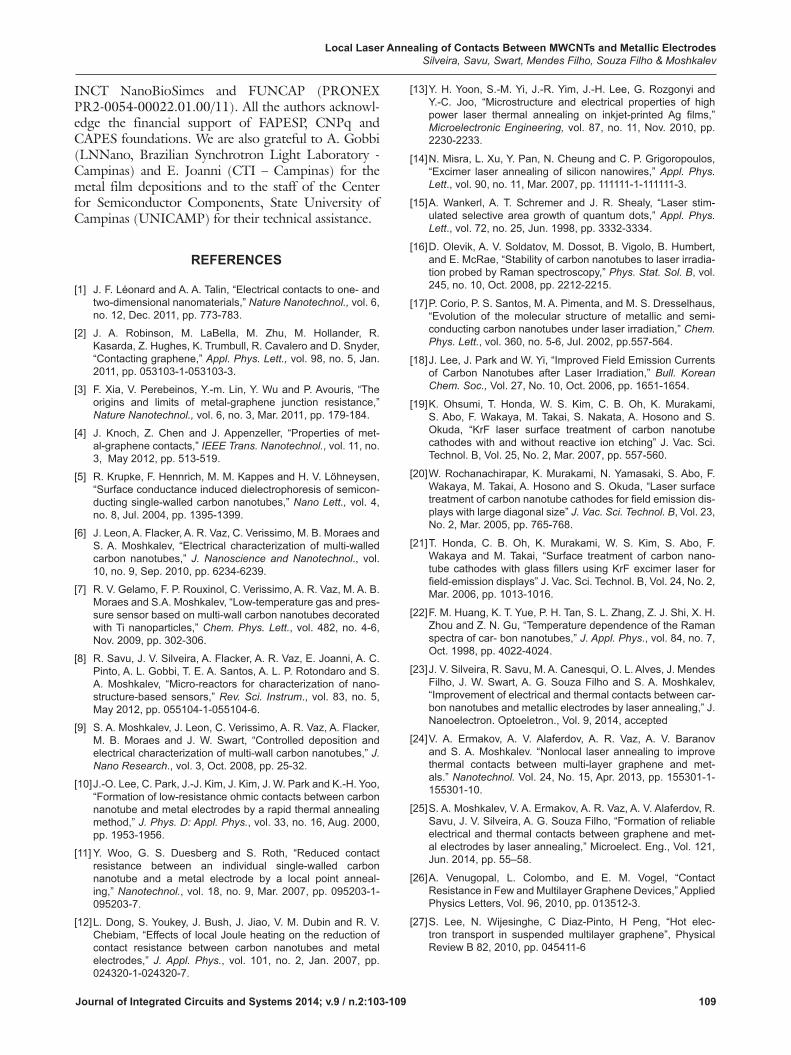
Laser treatments based on the R#3 route (with gradual increase of the laser power density) were ap-plied to nine samples (arrays of nanotubes) deposited over Au, Ti and W electrodes, three samples for each metal type. In a standard procedure, three laser scans (Raman maps) were made for each sample, with in-creasing PDs of 200 kW/cm2, 500 kW/cm2 and 900 kW/cm2, respectively, and nanotube burning did not occur during this process. The measurements of the electrical resistances before and after the three laser scans are shown in Figure 6.
Higher initial resistances, usually in the range from 1 to 10 MΩ, were observed for W and Ti elec-trodes. After laser treatment, one to three orders of magnitude drop of the electrical resistance was ob-tained (40-400 kΩ). Lower initial electrical resistance values were observed for Au, being between 20 and 50 kΩ and smaller resistance improvement, up to one order of magnitude, can be seen (to 3-30 kΩ) after
Figure 6. Electrical resistance for the MWCNTs deposited over W, Ti and Au electrodes measured as deposited and after laser treatment. Three samples were tested for each type of metal.
Local Laser Annealing of Contacts Between MWCNTs and Metallic Electrodes Silveira, Savu, Swart, Mendes Filho, Souza Filho & Moshkalev
109Journal of Integrated Circuits and Systems 2014; v.9 / n.2:103-109
INCT NanoBioSimes and FUNCAP (PRONEX PR2-0054-00022.01.00/11). All the authors acknowl-edge the financial support of FAPESP, CNPq and CAPES foundations. We are also grateful to A. Gobbi (LNNano, Brazilian Synchrotron Light Laboratory - Campinas) and E. Joanni (CTI – Campinas) for the metal film depositions and to the staff of the Center for Semiconductor Components, State University of Campinas (UNICAMP) for their technical assistance.
REFERENCES
[1] J. F. Léonard and A. A. Talin, “Electrical contacts to one- and two-dimensional nanomaterials,” Nature Nanotechnol., vol. 6, no. 12, Dec. 2011, pp. 773-783.
[2] J. A. Robinson, M. LaBella, M. Zhu, M. Hollander, R. Kasarda, Z. Hughes, K. Trumbull, R. Cavalero and D. Snyder, “Contacting graphene,” Appl. Phys. Lett., vol. 98, no. 5, Jan. 2011, pp. 053103-1-053103-3.
[3] F. Xia, V. Perebeinos, Y.-m. Lin, Y. Wu and P. Avouris, “The origins and limits of metal-graphene junction resistance,” Nature Nanotechnol., vol. 6, no. 3, Mar. 2011, pp. 179-184.
[4] J. Knoch, Z. Chen and J. Appenzeller, “Properties of met-al-graphene contacts,” IEEE Trans. Nanotechnol., vol. 11, no. 3, May 2012, pp. 513-519.
[5] R. Krupke, F. Hennrich, M. M. Kappes and H. V. Löhneysen, “Surface conductance induced dielectrophoresis of semicon-ducting single-walled carbon nanotubes,” Nano Lett., vol. 4, no. 8, Jul. 2004, pp. 1395-1399.
[6] J. Leon, A. Flacker, A. R. Vaz, C. Verissimo, M. B. Moraes and S. A. Moshkalev, “Electrical characterization of multi-walled carbon nanotubes,” J. Nanoscience and Nanotechnol., vol. 10, no. 9, Sep. 2010, pp. 6234-6239.
[7] R. V. Gelamo, F. P. Rouxinol, C. Verissimo, A. R. Vaz, M. A. B. Moraes and S.A. Moshkalev, “Low-temperature gas and pres-sure sensor based on multi-wall carbon nanotubes decorated with Ti nanoparticles,” Chem. Phys. Lett., vol. 482, no. 4-6, Nov. 2009, pp. 302-306.
[8] R. Savu, J. V. Silveira, A. Flacker, A. R. Vaz, E. Joanni, A. C. Pinto, A. L. Gobbi, T. E. A. Santos, A. L. P. Rotondaro and S. A. Moshkalev, “Micro-reactors for characterization of nano-structure-based sensors,” Rev. Sci. Instrum., vol. 83, no. 5, May 2012, pp. 055104-1-055104-6.
[9] S. A. Moshkalev, J. Leon, C. Verissimo, A. R. Vaz, A. Flacker, M. B. Moraes and J. W. Swart, “Controlled deposition and electrical characterization of multi-wall carbon nanotubes,” J. Nano Research., vol. 3, Oct. 2008, pp. 25-32.
[10] J.-O. Lee, C. Park, J.-J. Kim, J. Kim, J. W. Park and K.-H. Yoo, “Formation of low-resistance ohmic contacts between carbon nanotube and metal electrodes by a rapid thermal annealing method,” J. Phys. D: Appl. Phys., vol. 33, no. 16, Aug. 2000, pp. 1953-1956.
[11] Y. Woo, G. S. Duesberg and S. Roth, “Reduced contact resistance between an individual single-walled carbon nanotube and a metal electrode by a local point anneal-ing,” Nanotechnol., vol. 18, no. 9, Mar. 2007, pp. 095203-1-095203-7.
[12] L. Dong, S. Youkey, J. Bush, J. Jiao, V. M. Dubin and R. V. Chebiam, “Effects of local Joule heating on the reduction of contact resistance between carbon nanotubes and metal electrodes,” J. Appl. Phys., vol. 101, no. 2, Jan. 2007, pp. 024320-1-024320-7.
[13] Y. H. Yoon, S.-M. Yi, J.-R. Yim, J.-H. Lee, G. Rozgonyi and Y.-C. Joo, “Microstructure and electrical properties of high power laser thermal annealing on inkjet-printed Ag films,” Microelectronic Engineering, vol. 87, no. 11, Nov. 2010, pp. 2230-2233.
[14] N. Misra, L. Xu, Y. Pan, N. Cheung and C. P. Grigoropoulos, “Excimer laser annealing of silicon nanowires,” Appl. Phys. Lett., vol. 90, no. 11, Mar. 2007, pp. 111111-1-111111-3.
[15] A. Wankerl, A. T. Schremer and J. R. Shealy, “Laser stim-ulated selective area growth of quantum dots,” Appl. Phys. Lett., vol. 72, no. 25, Jun. 1998, pp. 3332-3334.
[16] D. Olevik, A. V. Soldatov, M. Dossot, B. Vigolo, B. Humbert, and E. McRae, “Stability of carbon nanotubes to laser irradia-tion probed by Raman spectroscopy,” Phys. Stat. Sol. B, vol. 245, no. 10, Oct. 2008, pp. 2212-2215.
[17] P. Corio, P. S. Santos, M. A. Pimenta, and M. S. Dresselhaus, “Evolution of the molecular structure of metallic and semi-conducting carbon nanotubes under laser irradiation,” Chem. Phys. Lett., vol. 360, no. 5-6, Jul. 2002, pp.557-564.
[18] J. Lee, J. Park and W. Yi, “Improved Field Emission Currents of Carbon Nanotubes after Laser Irradiation,” Bull. Korean Chem. Soc., Vol. 27, No. 10, Oct. 2006, pp. 1651-1654.
[19] K. Ohsumi, T. Honda, W. S. Kim, C. B. Oh, K. Murakami, S. Abo, F. Wakaya, M. Takai, S. Nakata, A. Hosono and S. Okuda, “KrF laser surface treatment of carbon nanotube cathodes with and without reactive ion etching” J. Vac. Sci. Technol. B, Vol. 25, No. 2, Mar. 2007, pp. 557-560.
[20] W. Rochanachirapar, K. Murakami, N. Yamasaki, S. Abo, F. Wakaya, M. Takai, A. Hosono and S. Okuda, “Laser surface treatment of carbon nanotube cathodes for field emission dis-plays with large diagonal size” J. Vac. Sci. Technol. B, Vol. 23, No. 2, Mar. 2005, pp. 765-768.
[21] T. Honda, C. B. Oh, K. Murakami, W. S. Kim, S. Abo, F. Wakaya and M. Takai, “Surface treatment of carbon nano-tube cathodes with glass fillers using KrF excimer laser for field-emission displays” J. Vac. Sci. Technol. B, Vol. 24, No. 2, Mar. 2006, pp. 1013-1016.
[22] F. M. Huang, K. T. Yue, P. H. Tan, S. L. Zhang, Z. J. Shi, X. H. Zhou and Z. N. Gu, “Temperature dependence of the Raman spectra of car- bon nanotubes,” J. Appl. Phys., vol. 84, no. 7, Oct. 1998, pp. 4022-4024.
[23] J. V. Silveira, R. Savu, M. A. Canesqui, O. L. Alves, J. Mendes Filho, J. W. Swart, A. G. Souza Filho and S. A. Moshkalev, “Improvement of electrical and thermal contacts between car-bon nanotubes and metallic electrodes by laser annealing,” J. Nanoelectron. Optoeletron., Vol. 9, 2014, accepted
[24] V. A. Ermakov, A. V. Alaferdov, A. R. Vaz, A. V. Baranov and S. A. Moshkalev. “Nonlocal laser annealing to improve thermal contacts between multi-layer graphene and met-als.” Nanotechnol. Vol. 24, No. 15, Apr. 2013, pp. 155301-1-155301-10.
[25] S. A. Moshkalev, V. A. Ermakov, A. R. Vaz, A. V. Alaferdov, R. Savu, J. V. Silveira, A. G. Souza Filho, “Formation of reliable electrical and thermal contacts between graphene and met-al electrodes by laser annealing,” Microelect. Eng., Vol. 121, Jun. 2014, pp. 55–58.
[26] A. Venugopal, L. Colombo, and E. M. Vogel, “Contact Resistance in Few and Multilayer Graphene Devices,” Applied Physics Letters, Vol. 96, 2010, pp. 013512-3.
[27] S. Lee, N. Wijesinghe, C Diaz-Pinto, H Peng, “Hot elec-tron transport in suspended multilayer graphene”, Physical Review B 82, 2010, pp. 045411-6


![NANO EXPRESS Open Access Flow-induced voltage ......liquid [1]. Similar experiments were conducted with multi-walled carbon nanotubes (MWCNTs) [3]. The aligned MWCNTs were found to](https://img.pdfslide.net/doc/110x75/60cc1ccfc265ec2fa524fd51/nano-express-open-access-flow-induced-voltage-liquid-1-similar-experiments.jpg)