Embed Size (px)
Citation preview
1
Synchronous Sequential Logic
Logic and Digital System Design - CS 303Erkay Savaş
Sabanci University
2
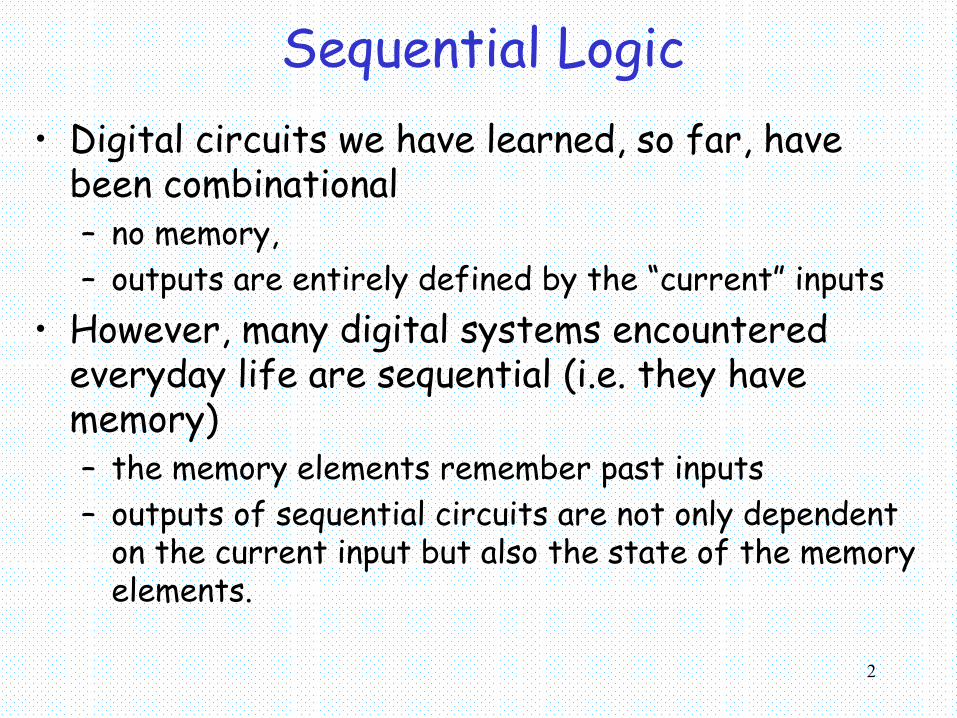
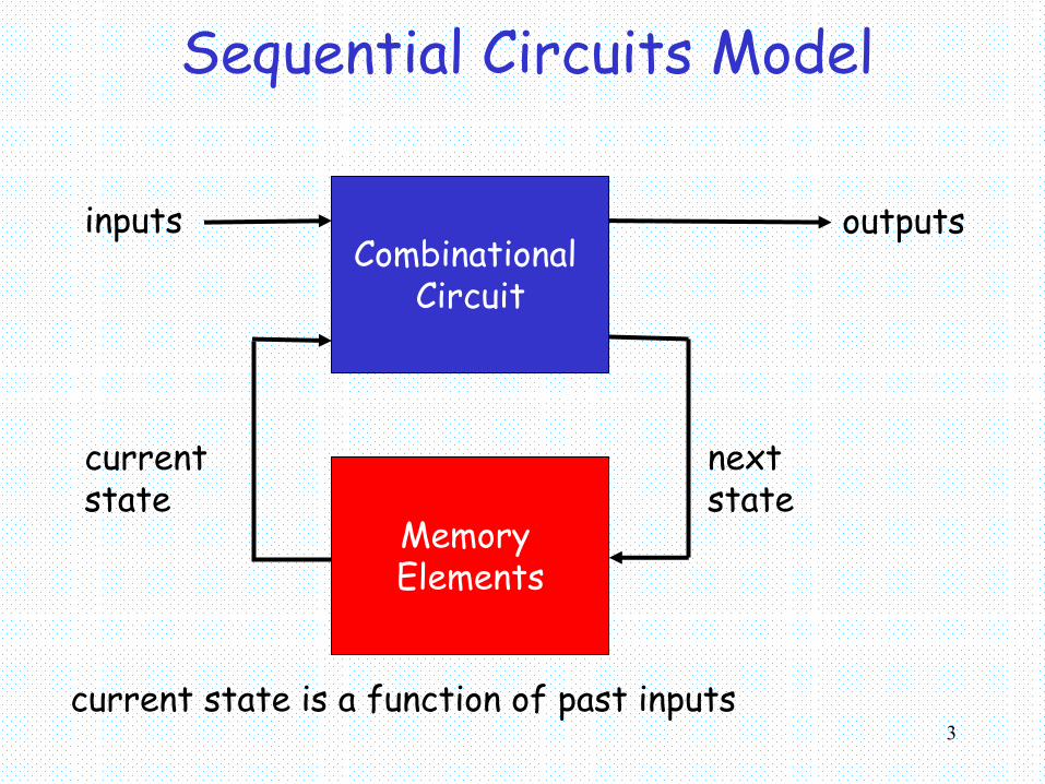
Sequential Logic• Digital circuits we have learned, so far, have
been combinational– no memory,– outputs are entirely defined by the “current” inputs
• However, many digital systems encountered everyday life are sequential (i.e. they have memory)– the memory elements remember past inputs– outputs of sequential circuits are not only dependent
on the current input but also the state of the memory elements.
3
Sequential Circuits Model
Combinational Circuit
inputs outputs
Memory Elements
currentstate
nextstate
current state is a function of past inputs
4
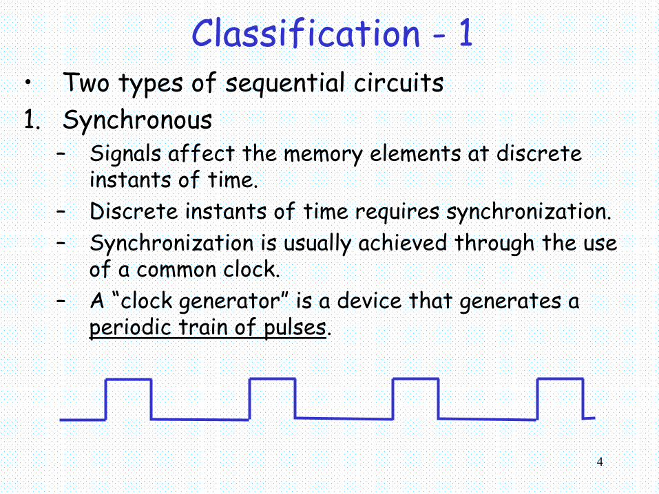
Classification - 1• Two types of sequential circuits1. Synchronous
– Signals affect the memory elements at discrete instants of time.
– Discrete instants of time requires synchronization.– Synchronization is usually achieved through the use
of a common clock.– A “clock generator” is a device that generates a
periodic train of pulses.
5
Classification - 21. Synchronous
• The state of the memory elements are updated with the arrival of each pulse
• This type of logical circuit is also known as clocked sequential circuits.
2. Asynchronous• No clock• behavior of an asynchronous sequential circuits
depends upon the input signals at any instant of time and the order in which the inputs change.
• Memory elements in asynchronous circuits are regarded as time-delay elements
6
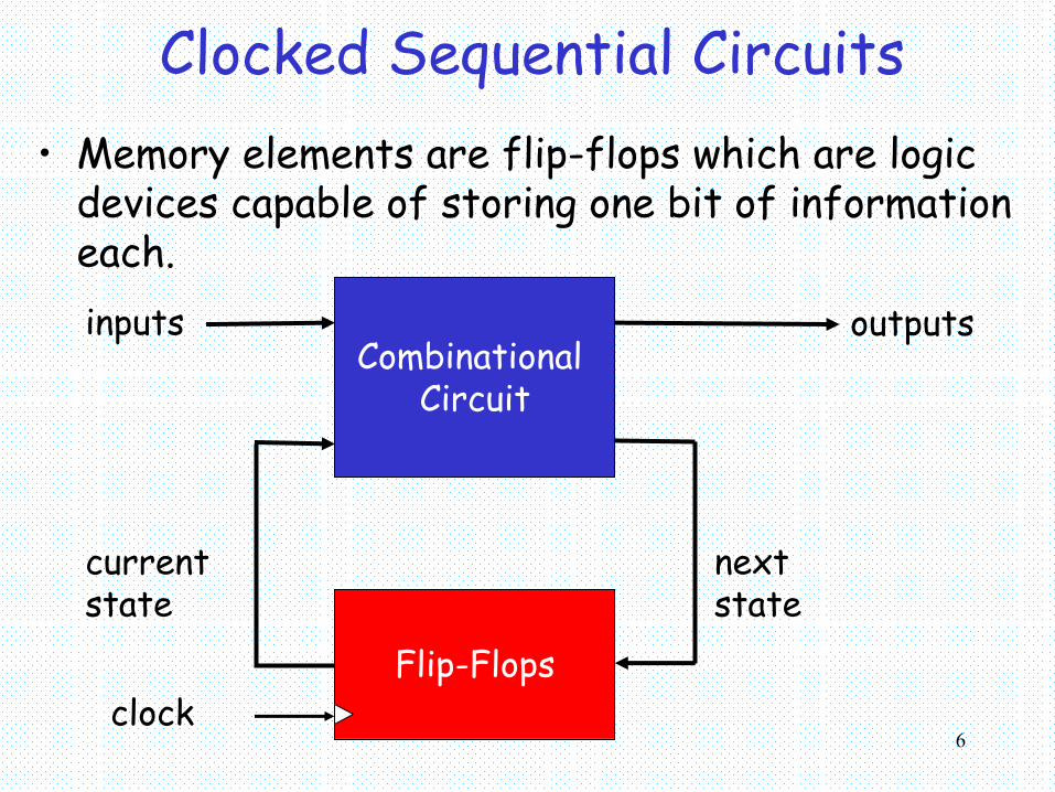
Clocked Sequential Circuits• Memory elements are flip-flops which are logic
devices capable of storing one bit of information each.
Combinational Circuit
Flip-Flops
inputs outputs
currentstate
nextstate
clock
7
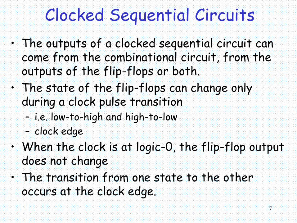
Clocked Sequential Circuits• The outputs of a clocked sequential circuit can
come from the combinational circuit, from the outputs of the flip-flops or both.
• The state of the flip-flops can change only during a clock pulse transition – i.e. low-to-high and high-to-low– clock edge
• When the clock is at logic-0, the flip-flop output does not change
• The transition from one state to the other occurs at the clock edge.
8
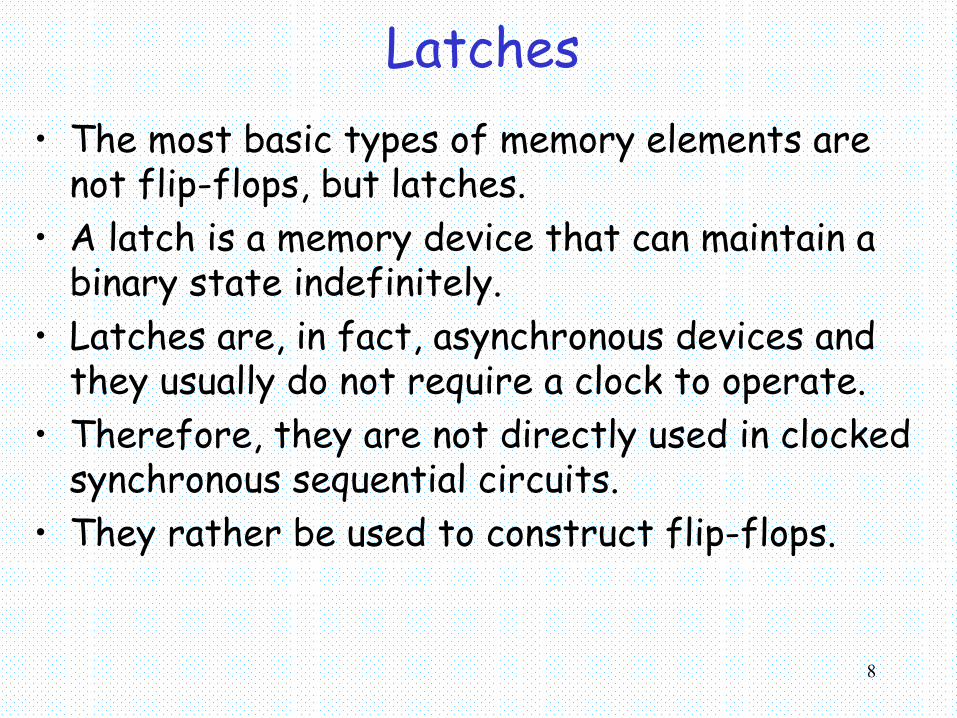
Latches• The most basic types of memory elements are
not flip-flops, but latches.• A latch is a memory device that can maintain a
binary state indefinitely.• Latches are, in fact, asynchronous devices and
they usually do not require a clock to operate.• Therefore, they are not directly used in clocked
synchronous sequential circuits.• They rather be used to construct flip-flops.
9
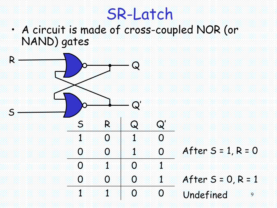
SR-Latch• A circuit is made of cross-coupled NOR (or
NAND) gatesR Q
SQ’
00111000101001000101Q’QRS
After S = 1, R = 0
After S = 0, R = 1Undefined
10
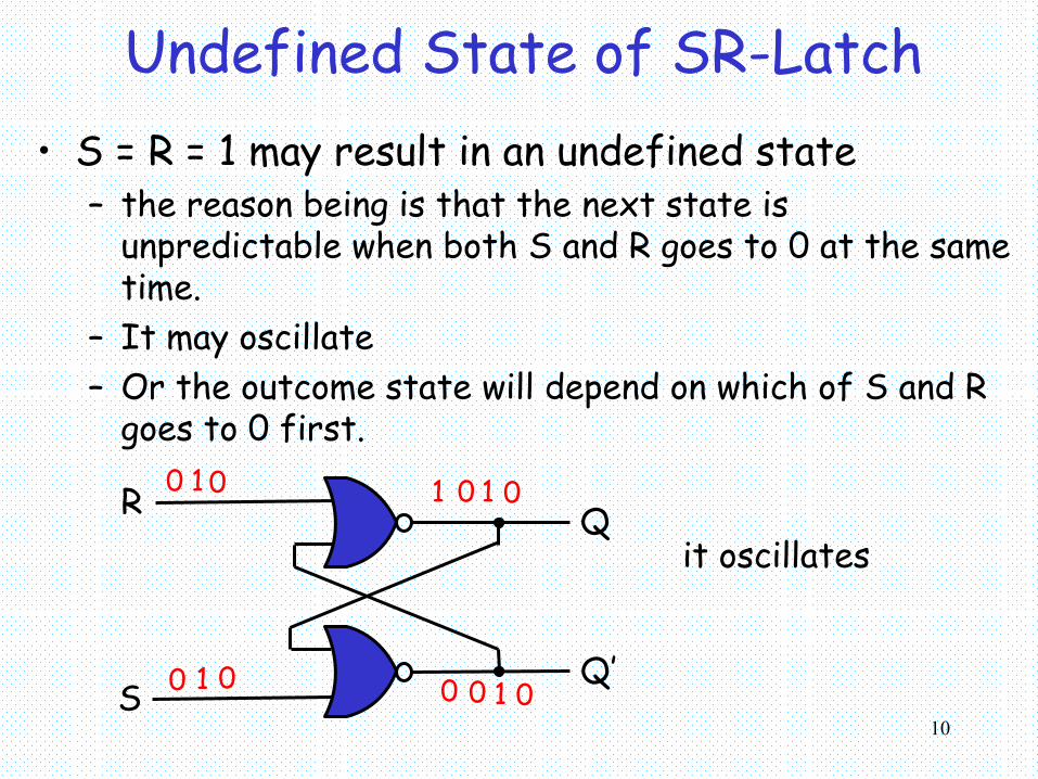
Undefined State of SR-Latch• S = R = 1 may result in an undefined state
– the reason being is that the next state is unpredictable when both S and R goes to 0 at the same time.
– It may oscillate– Or the outcome state will depend on which of S and R
goes to 0 first.
R Q
SQ’
0
0
1
0
1
1
0
0
0
0
1
1
0
0
it oscillates
11
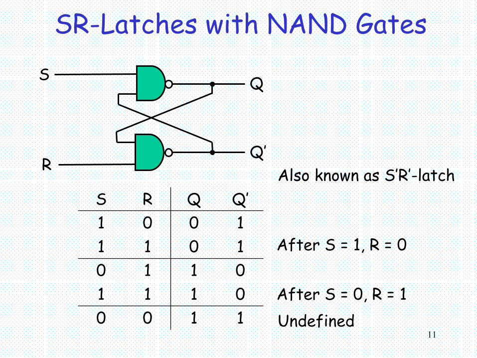
SR-Latches with NAND GatesS Q
RQ’
11000111011010111001
Q’QRS
After S = 1, R = 0
After S = 0, R = 1Undefined
Also known as S’R’-latch
12
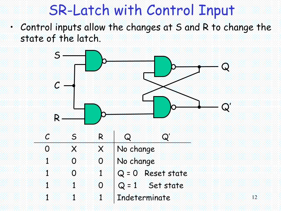
SR-Latch with Control Input• Control inputs allow the changes at S and R to change the
state of the latch.
Q
Q’R
S
C
Indeterminate111Set stateQ = 1011
Reset stateQ = 0101No change001No changeXX0
Q’QRSC
13
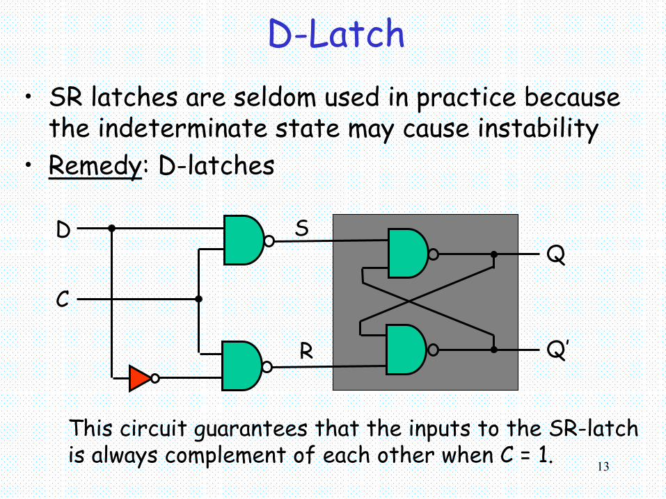
D-Latch• SR latches are seldom used in practice because
the indeterminate state may cause instability• Remedy: D-latches
R
QS
Q’
This circuit guarantees that the inputs to the SR-latchis always complement of each other when C = 1.
C
D
14
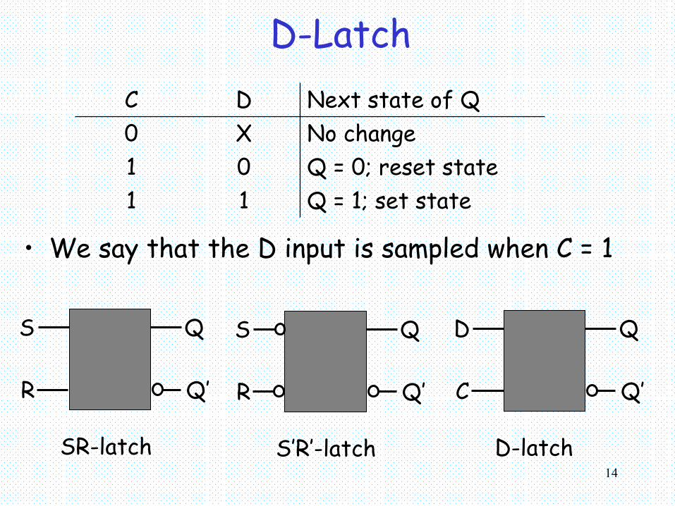
D-Latch
• We say that the D input is sampled when C = 1
Q = 1; set state11Q = 0; reset state01No changeX0Next state of QDC
S
R
Q
Q’
SR-latch
S
R
Q
Q’
S’R’-latch
D
C
Q
Q’
D-latch
15
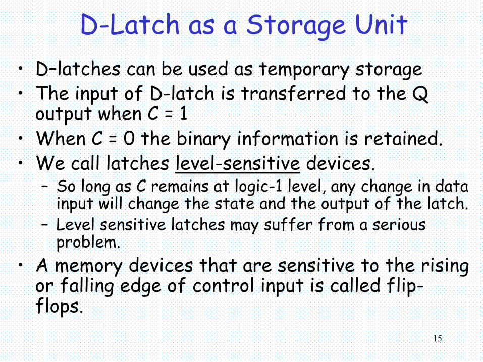
D-Latch as a Storage Unit• D–latches can be used as temporary storage• The input of D-latch is transferred to the Q
output when C = 1 • When C = 0 the binary information is retained.• We call latches level-sensitive devices.
– So long as C remains at logic-1 level, any change in data input will change the state and the output of the latch.
– Level sensitive latches may suffer from a serious problem.
• A memory devices that are sensitive to the rising or falling edge of control input is called flip-flops.
16
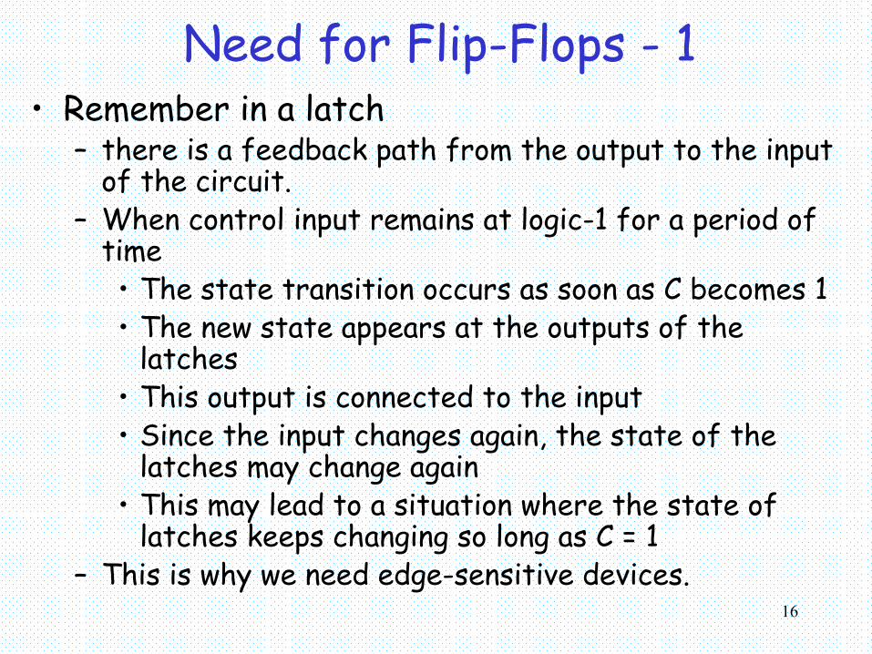
Need for Flip-Flops - 1• Remember in a latch
– there is a feedback path from the output to the input of the circuit.
– When control input remains at logic-1 for a period of time• The state transition occurs as soon as C becomes 1• The new state appears at the outputs of the
latches • This output is connected to the input• Since the input changes again, the state of the
latches may change again• This may lead to a situation where the state of
latches keeps changing so long as C = 1– This is why we need edge-sensitive devices.
17
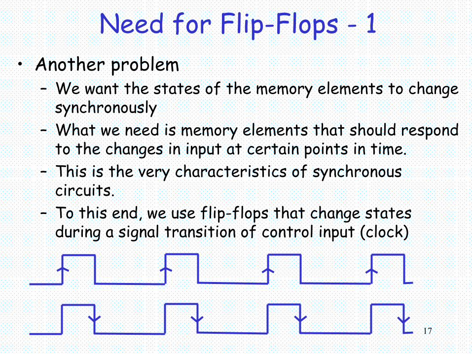
Need for Flip-Flops - 1• Another problem
– We want the states of the memory elements to change synchronously
– What we need is memory elements that should respond to the changes in input at certain points in time.
– This is the very characteristics of synchronous circuits.
– To this end, we use flip-flops that change states during a signal transition of control input (clock)
18
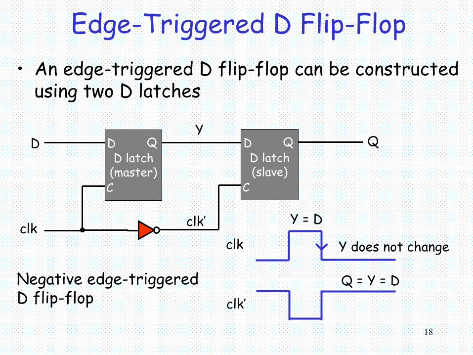
Edge-Triggered D Flip-Flop• An edge-triggered D flip-flop can be constructed
using two D latches
D latch(master)
D
C
QD latch(slave)
D
C
Q
clk
D QY
clk’
Q = Y = D
Y = D
clk Y does not change
Negative edge-triggered D flip-flop
clk’
19
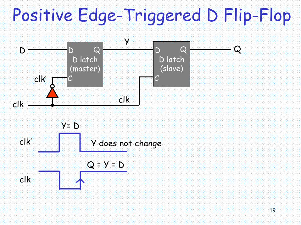
Positive Edge-Triggered D Flip-Flop
D latch(master)
D
C
QD latch(slave)
D
C
QD
clk
QY
clk
clk’
Y= D
clk’ Y does not change
clk
Q = Y = D
20
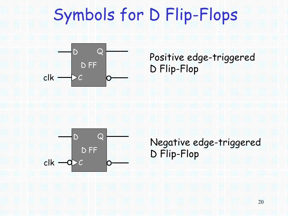
Symbols for D Flip-Flops
D FF
D Q
clk C
Positive edge-triggeredD Flip-Flop
D FF
D Q
clk C
Negative edge-triggeredD Flip-Flop
21
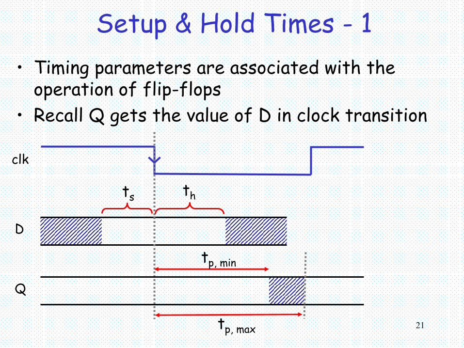
Setup & Hold Times - 1• Timing parameters are associated with the
operation of flip-flops• Recall Q gets the value of D in clock transition
clk
D
Q
ts th
tp, min
tp, max
22
Setup & Hold Times - 2• Setup time, ts
– The change in the input D must be made before the clock transition.
– Input D must maintain this new value for a certain minimum amount time.
– If a change occurs at D less than ts second before the clock transition, then the output may not acquire this new value.
– It may even demonstrate unstable behavior.• Hold time, th,
– Similarly the value at D must be maintained for a minimum amount of time (i.e. th) after the clock transition.
23
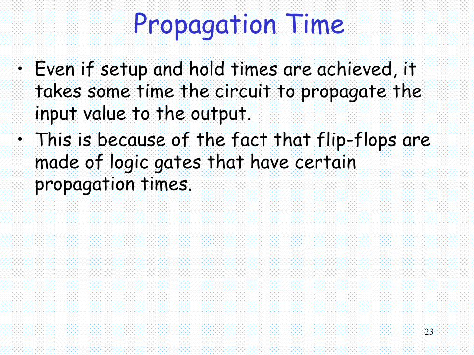
Propagation Time• Even if setup and hold times are achieved, it
takes some time the circuit to propagate the input value to the output.
• This is because of the fact that flip-flops are made of logic gates that have certain propagation times.
24
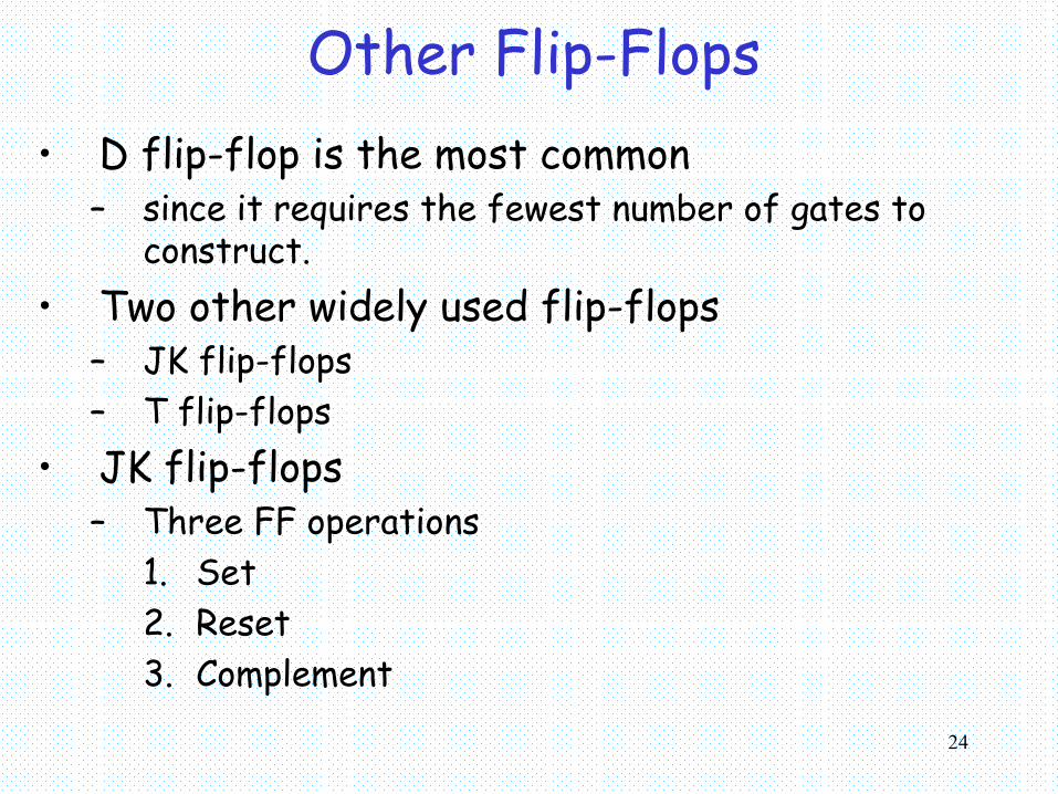
Other Flip-Flops• D flip-flop is the most common
– since it requires the fewest number of gates to construct.
• Two other widely used flip-flops– JK flip-flops – T flip-flops
• JK flip-flops– Three FF operations
1. Set2. Reset 3. Complement
25
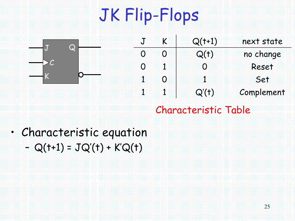
JK Flip-Flops
• Characteristic equation– Q(t+1) = JQ’(t) + K’Q(t)
J Q
C
K
ComplementQ’(t)11Set101
Reset010no changeQ(t)00next stateQ(t+1)KJ
Characteristic Table
26
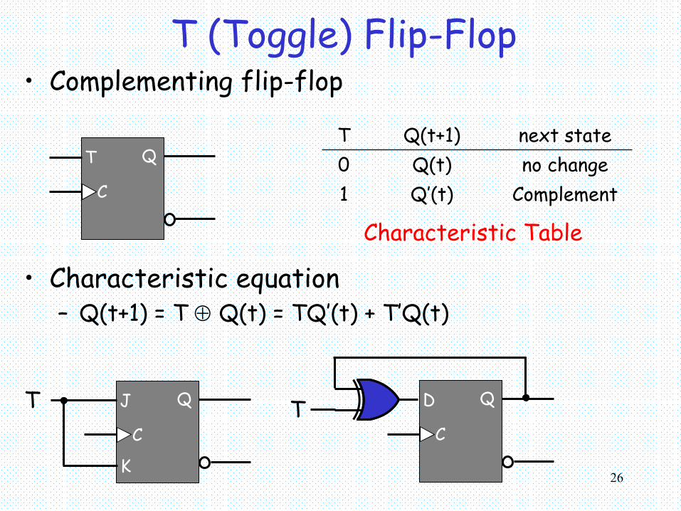
T (Toggle) Flip-Flop• Complementing flip-flop
T Q
C ComplementQ’(t)1no changeQ(t)0next stateQ(t+1)T
Characteristic Table
• Characteristic equation– Q(t+1) = T ⊕ Q(t) = TQ’(t) + T’Q(t)
J Q
C
K
T D Q
CT
27
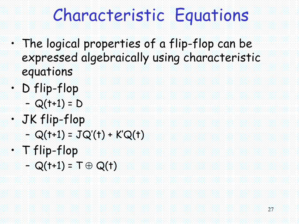
Characteristic Equations• The logical properties of a flip-flop can be
expressed algebraically using characteristic equations
• D flip-flop– Q(t+1) = D
• JK flip-flop– Q(t+1) = JQ’(t) + K’Q(t)
• T flip-flop– Q(t+1) = T ⊕ Q(t)
28
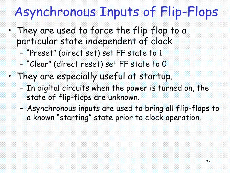
Asynchronous Inputs of Flip-Flops• They are used to force the flip-flop to a
particular state independent of clock– “Preset” (direct set) set FF state to 1– “Clear” (direct reset) set FF state to 0
• They are especially useful at startup.– In digital circuits when the power is turned on, the
state of flip-flops are unknown.– Asynchronous inputs are used to bring all flip-flops to
a known “starting” state prior to clock operation.
29
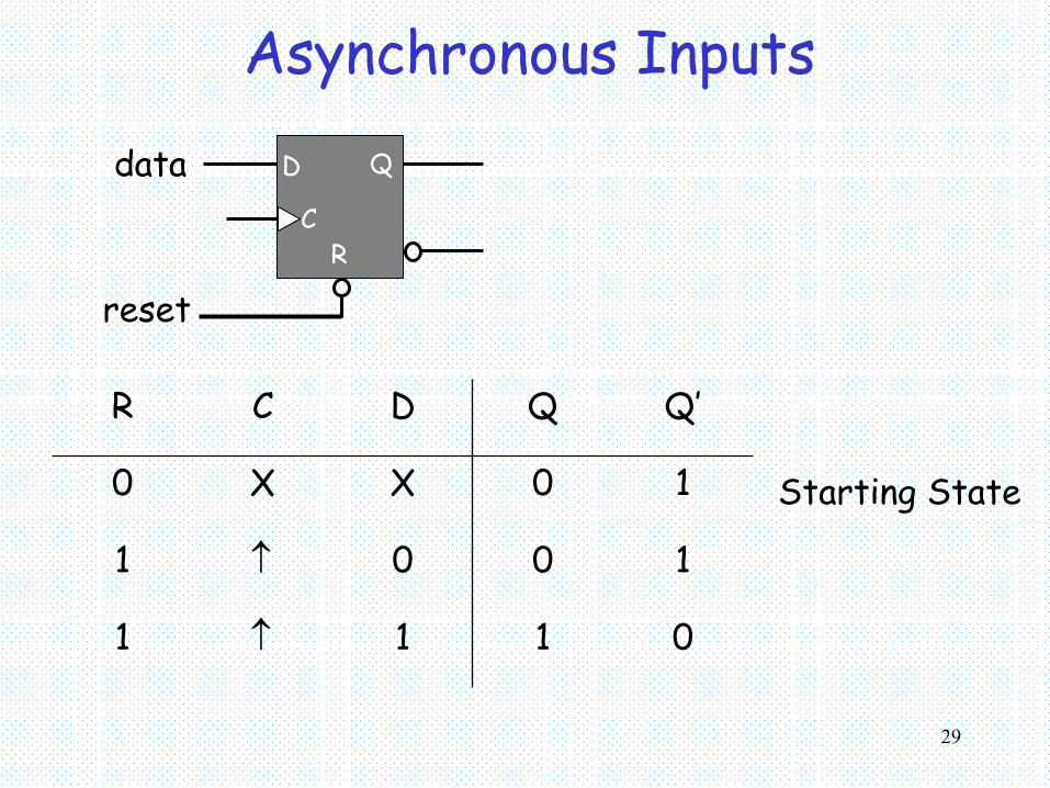
Asynchronous Inputs
011↑1
100↑1
10XX0
Q’QDCR
Starting State
D Q
C
data
resetR
30
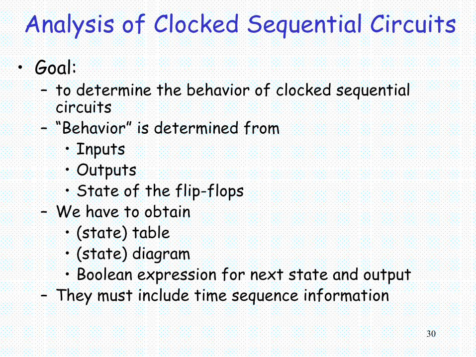
Analysis of Clocked Sequential Circuits• Goal:
– to determine the behavior of clocked sequential circuits
– “Behavior” is determined from• Inputs• Outputs • State of the flip-flops
– We have to obtain• (state) table• (state) diagram• Boolean expression for next state and output
– They must include time sequence information
31
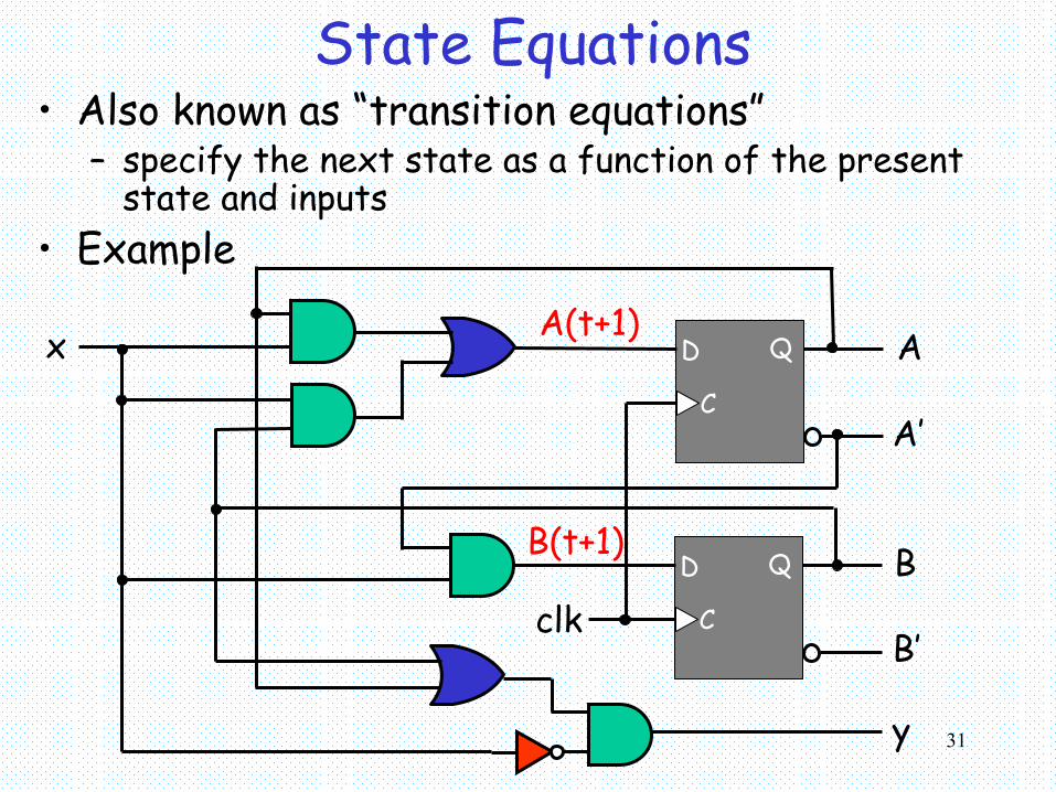
State Equations• Also known as “transition equations”
– specify the next state as a function of the present state and inputs
• ExampleA(t+1)
B(t+1)
D Q
C
D Q
C
A
A’
B
B’
x
y
clk
32
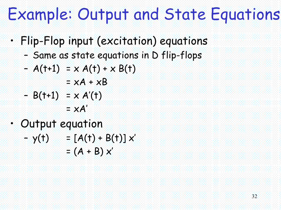
Example: Output and State Equations• Flip-Flop input (excitation) equations
– Same as state equations in D flip-flops– A(t+1) = x A(t) + x B(t)
= xA + xB– B(t+1) = x A’(t)
= xA’ • Output equation
– y(t) = [A(t) + B(t)] x’= (A + B) x’
33
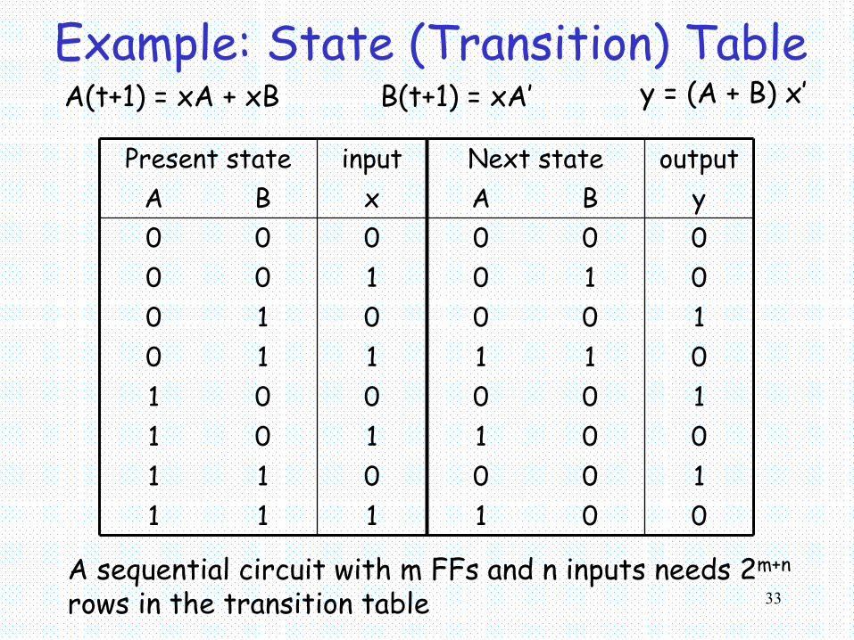
Example: State (Transition) Table
001100001100011100
111011101001110010
010100000000yBAxBA
outputNext stateinputPresent state
A sequential circuit with m FFs and n inputs needs 2m+n
rows in the transition table
A(t+1) = xA + xB B(t+1) = xA’ y = (A + B) x’
34
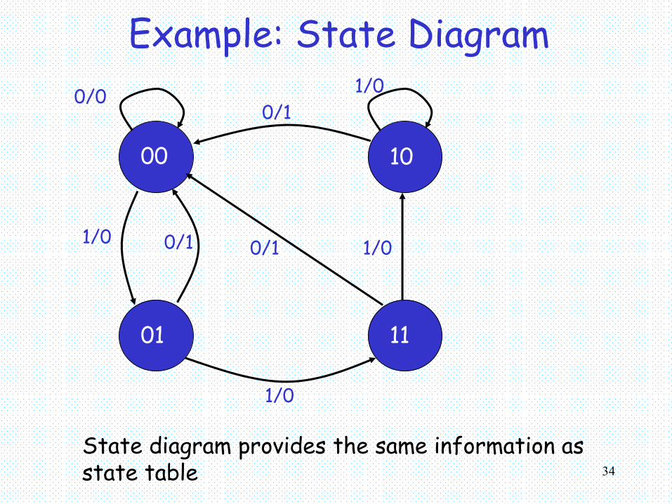
Example: State Diagram
00
01 11
10
0/0
1/0 0/1
1/0
1/00/1
0/1 1/0
State diagram provides the same information as state table
35
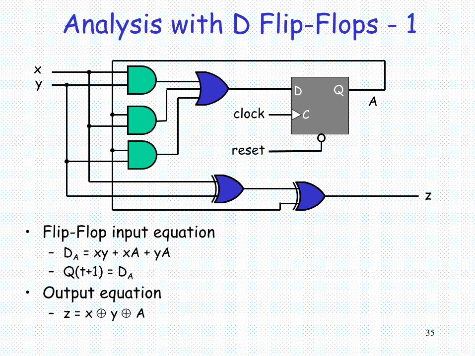
Analysis with D Flip-Flops - 1
D Q
C
xy
z
clock
reset
A
• Flip-Flop input equation– DA = xy + xA + yA– Q(t+1) = DA
• Output equation– z = x ⊕ y ⊕ A
36
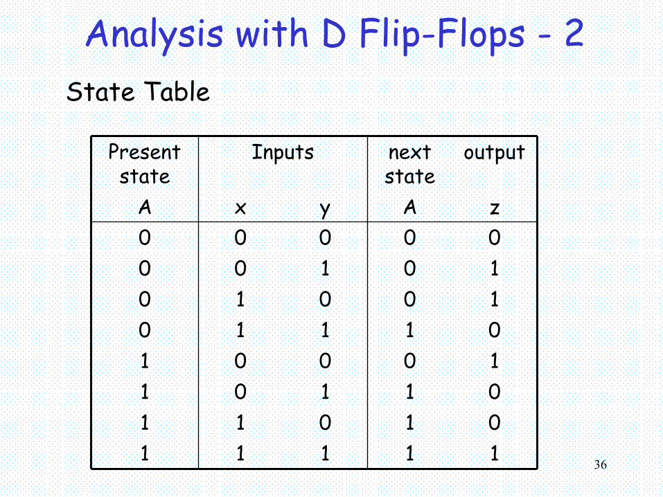
Analysis with D Flip-Flops - 2
outputnext state
InputsPresent state
1111101011011011000101110100101010000000zAyxA
State Table
37
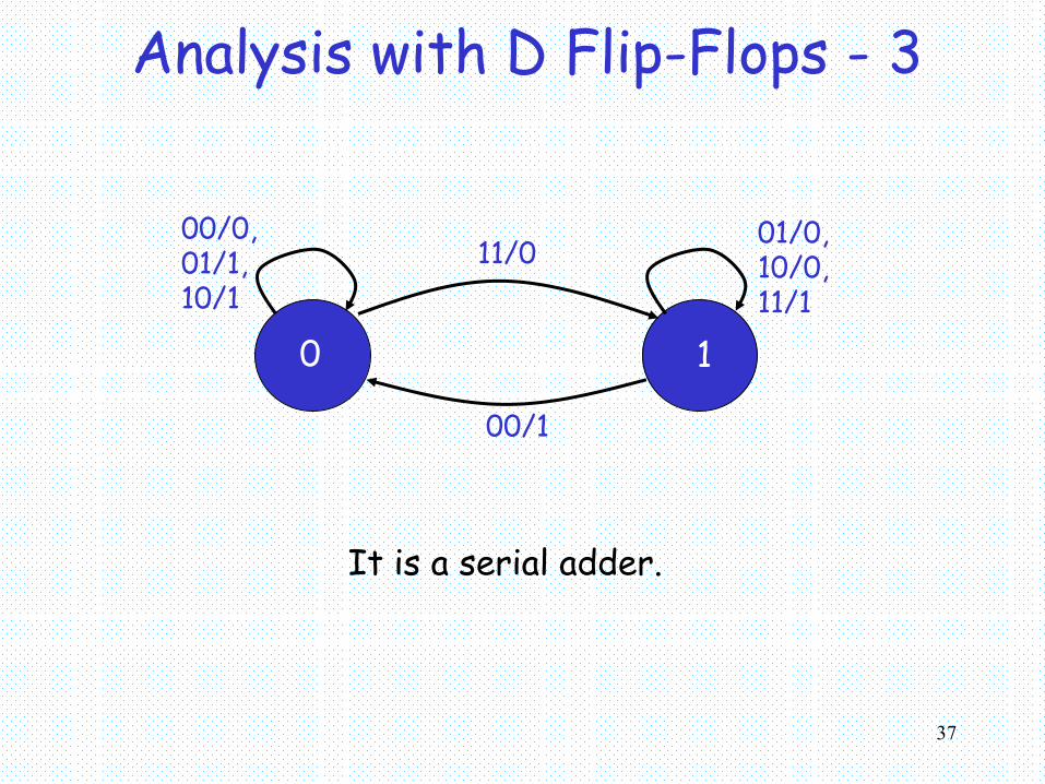
Analysis with D Flip-Flops - 3
0 1
00/0,01/1,10/1
11/0 01/0,10/0,11/1
00/1
It is a serial adder.
38
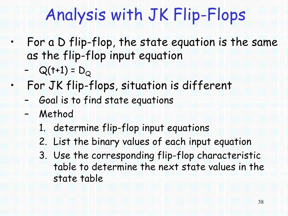
Analysis with JK Flip-Flops• For a D flip-flop, the state equation is the same
as the flip-flop input equation– Q(t+1) = DQ
• For JK flip-flops, situation is different– Goal is to find state equations– Method
1. determine flip-flop input equations2. List the binary values of each input equation3. Use the corresponding flip-flop characteristic
table to determine the next state values in the state table
39
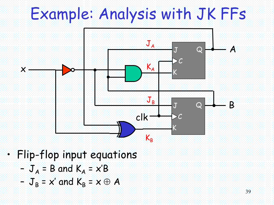
Example: Analysis with JK FFs
• Flip-flop input equations– JA = B and KA = x’B– JB = x’ and KB = x ⊕ A
JA
KA
JB
KB
J QC
D Q
C
A
B
x
clk
K
J QC
K
40
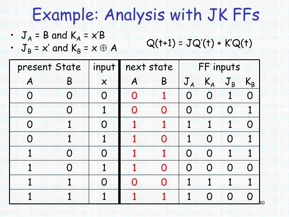
Example: Analysis with JK FFs• JA = B and KA = x’B• JB = x’ and KB = x ⊕ A
1011110
100101010
000111000110100011100010
11001100
111011101001110010100000
KBJBKAJABAxBAFF inputsnext stateinputpresent State
Q(t+1) = JQ’(t) + K’Q(t)
41
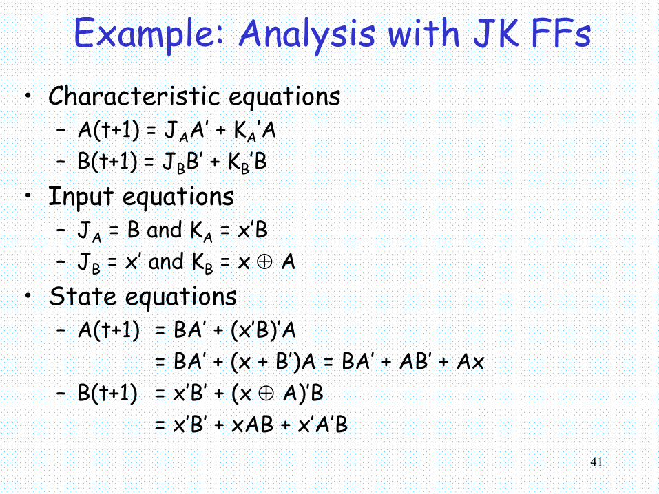
Example: Analysis with JK FFs• Characteristic equations
– A(t+1) = JAA’ + KA’A– B(t+1) = JBB’ + KB’B
• Input equations– JA = B and KA = x’B– JB = x’ and KB = x ⊕ A
• State equations– A(t+1) = BA’ + (x’B)’A
= BA’ + (x + B’)A = BA’ + AB’ + Ax – B(t+1) = x’B’ + (x ⊕ A)’B
= x’B’ + xAB + x’A’B
42
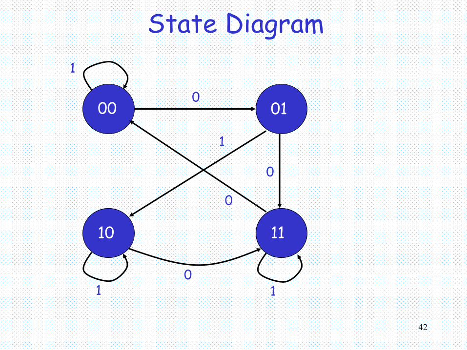
State Diagram
00
10 11
01
1
10
1
0
0
1
0
43
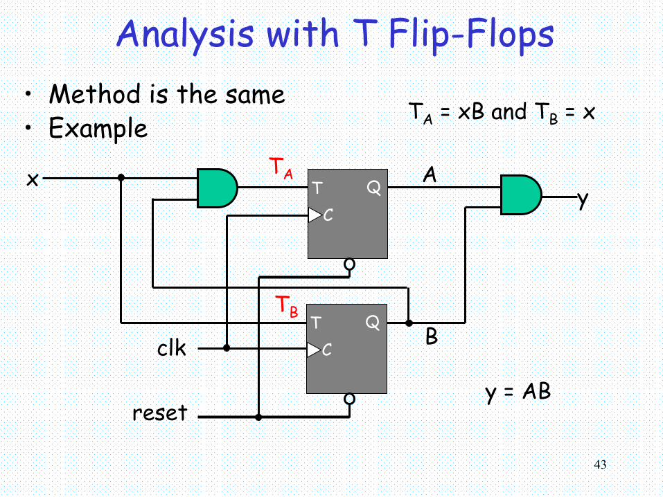
Analysis with T Flip-Flops• Method is the same• Example
TA
TB
TA = xB and TB = x
T QC
D Q
C
A
B
x
clkT Q
C
reset
y
y = AB
44
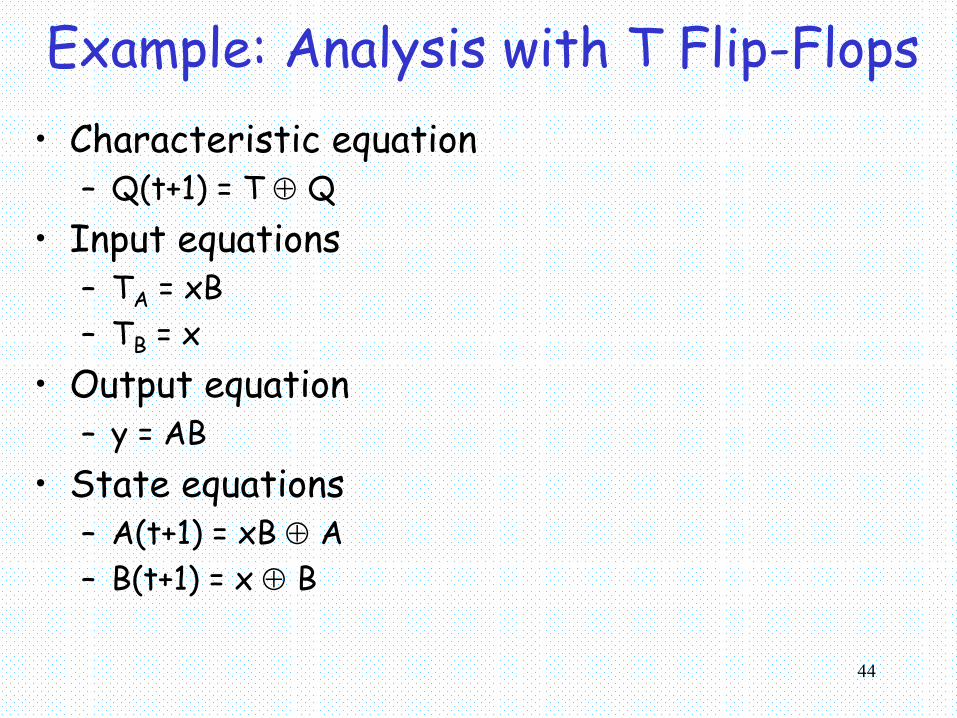
Example: Analysis with T Flip-Flops• Characteristic equation
– Q(t+1) = T ⊕ Q• Input equations
– TA = xB– TB = x
• Output equation– y = AB
• State equations– A(t+1) = xB ⊕ A– B(t+1) = x ⊕ B
45
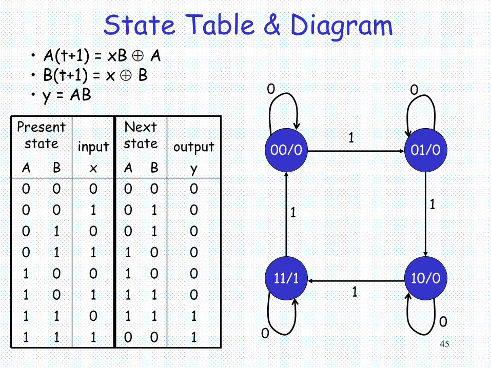
State Table & Diagram
100111111011011101001001001110010010010100000000yBAxBA
outputNext stateinput
Present state
• A(t+1) = xB ⊕ A• B(t+1) = x ⊕ B• y = AB
00/0
0 0
00
01/01
10/0
1
11/11
1
46
Mealy and Moore Models• There are two models for sequential circuits
– Mealy – Moore
• They differ in the way the outputs are generated– Mealy:
• output is a function of both present states and inputs
– Moore• output is a function of present state only
47
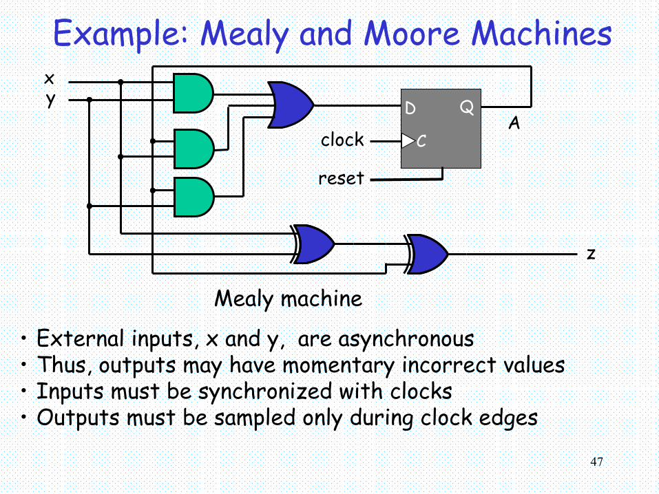
Example: Mealy and Moore Machines
D Q
C
xy
z
clock
reset
A
Mealy machine
• External inputs, x and y, are asynchronous • Thus, outputs may have momentary incorrect values• Inputs must be synchronized with clocks• Outputs must be sampled only during clock edges
48
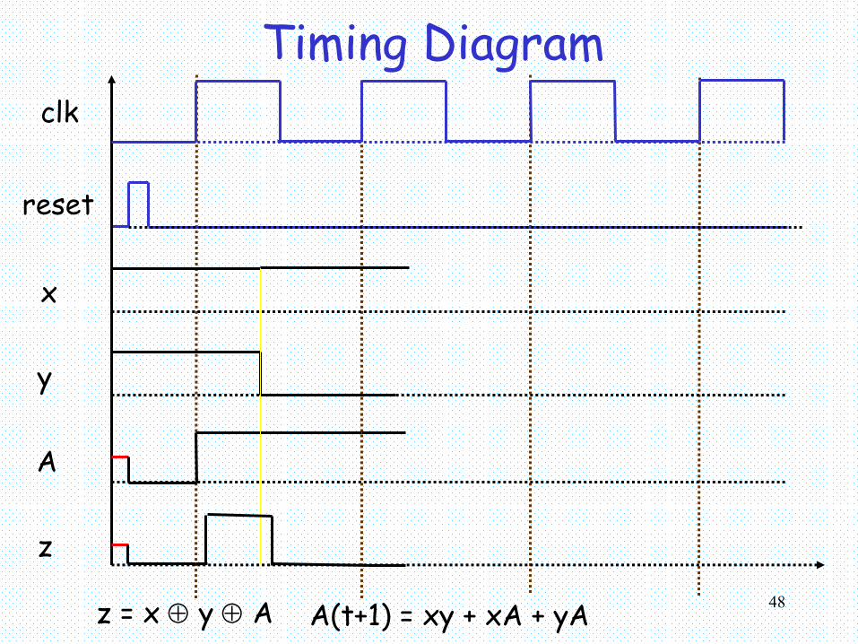
Timing Diagramclk
x
A
y
z
reset
z = x ⊕ y ⊕ A A(t+1) = xy + xA + yA
49
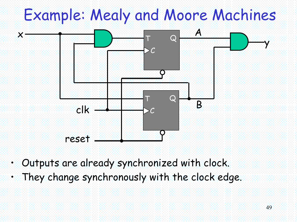
Example: Mealy and Moore Machines
• Outputs are already synchronized with clock.• They change synchronously with the clock edge.
T QC
D Q
C
A
B
x
clkT Q
C
reset
y
50
State Reduction and Assignment• In the design process of sequential circuits
certain techniques are useful in reducing the circuit complexity– state reduction– state assignment
• State reduction– Fewer states fewer number of flip-flops– m flip-flops 2m states– Example: m = 5 2m = 32
• If we reduce the number of states to 21 do we reduce the number of flip-flops?
51
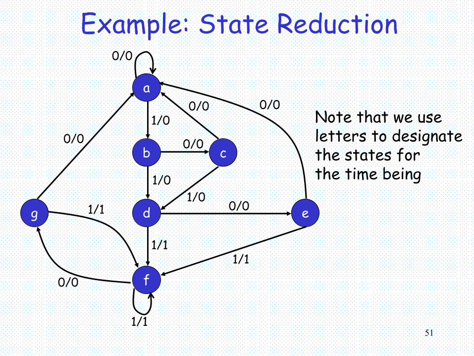
Example: State Reduction
a
b
d
f
c
eg
0/0
1/1
1/0
1/0
1/1
0/0
1/0
0/0
0/0
0/0
0/0
1/1
0/0
1/1
Note that we useletters to designate the states forthe time being
52
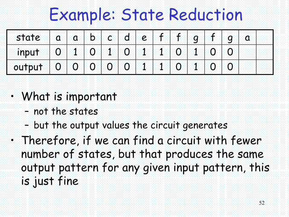
Example: State Reduction
• What is important– not the states– but the output values the circuit generates
• Therefore, if we can find a circuit with fewer number of states, but that produces the same output pattern for any given input pattern, this is just fine
00101100000output00101101010input
agfgffedcbaastate
53
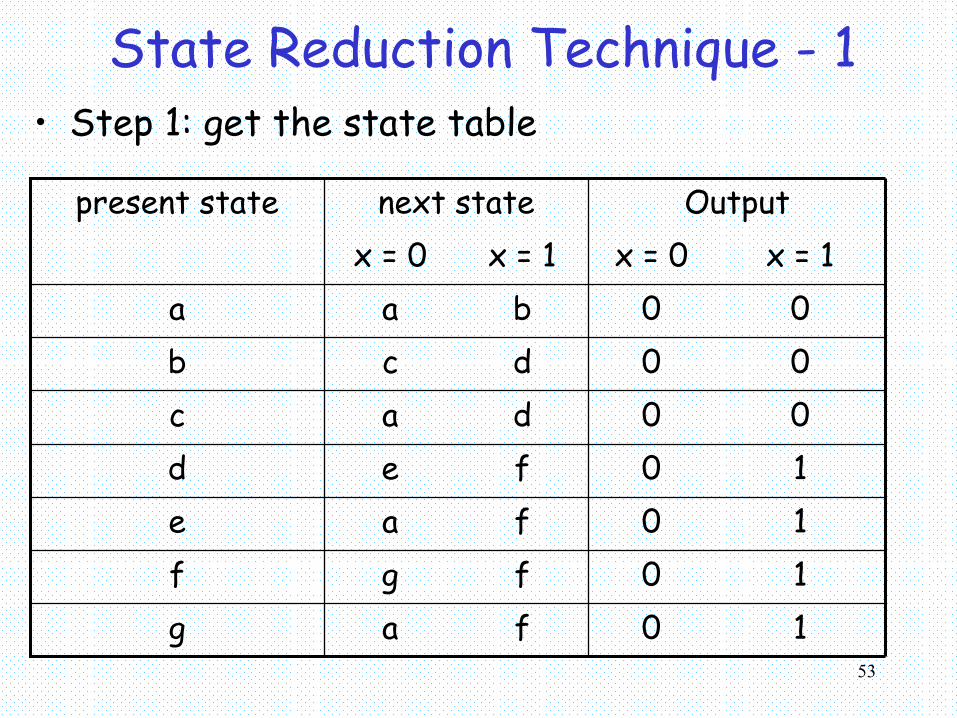
State Reduction Technique - 1 • Step 1: get the state table
10fgf10fag
10fae10fed00dac00dcb00baa
x = 1x = 0x = 1x = 0Outputnext statepresent state
54
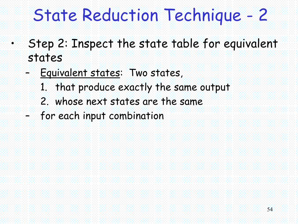
State Reduction Technique - 2• Step 2: Inspect the state table for equivalent
states– Equivalent states: Two states,
1. that produce exactly the same output2. whose next states are the same
– for each input combination
55
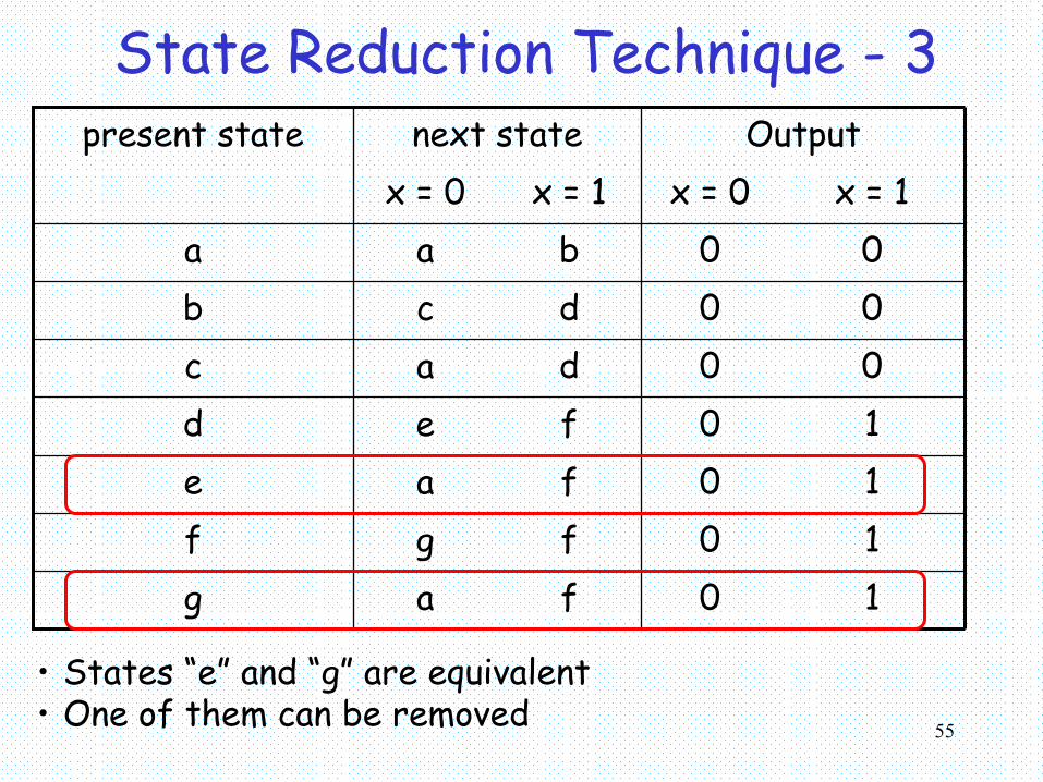
State Reduction Technique - 3
10fgf10fag
10fae10fed00dac00dcb00baa
x = 1x = 0x = 1x = 0Outputnext statepresent state
• States “e” and “g” are equivalent• One of them can be removed
56
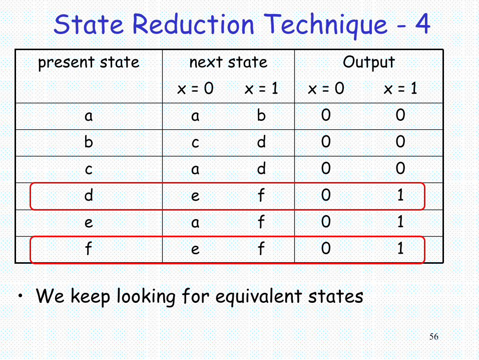
State Reduction Technique - 4
• We keep looking for equivalent states
10fef10fae10fed00dac00dcb00baa
x = 1x = 0x = 1x = 0Outputnext statepresent state
57
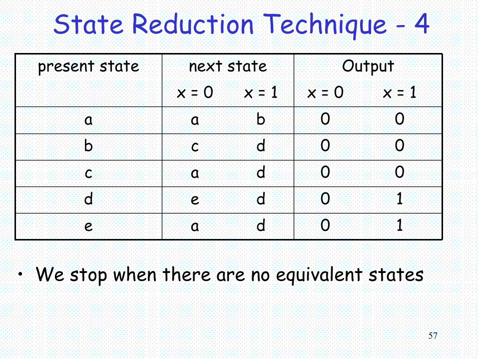
State Reduction Technique - 4
• We stop when there are no equivalent states
10dae10ded00dac00dcb00baa
x = 1x = 0x = 1x = 0Outputnext statepresent state
58
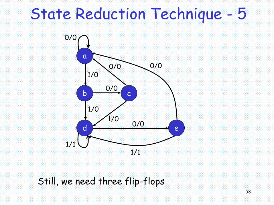
State Reduction Technique - 5
a
b
d
c
e
0/0
1/0
1/0
1/1
0/0
1/0
0/0
0/0
0/0
1/1
Still, we need three flip-flops
59
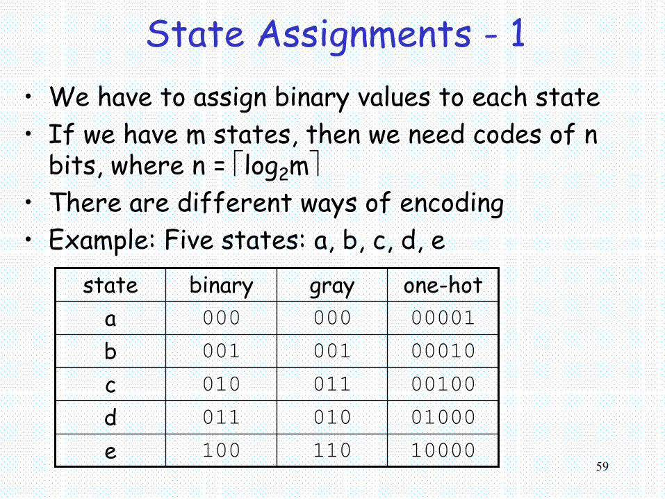
State Assignments - 1• We have to assign binary values to each state• If we have m states, then we need codes of n
bits, where n = log2m• There are different ways of encoding• Example: Five states: a, b, c, d, e
10000110100e01000010011d00100011010c00010001001b00001000000aone-hotgraybinarystate
60
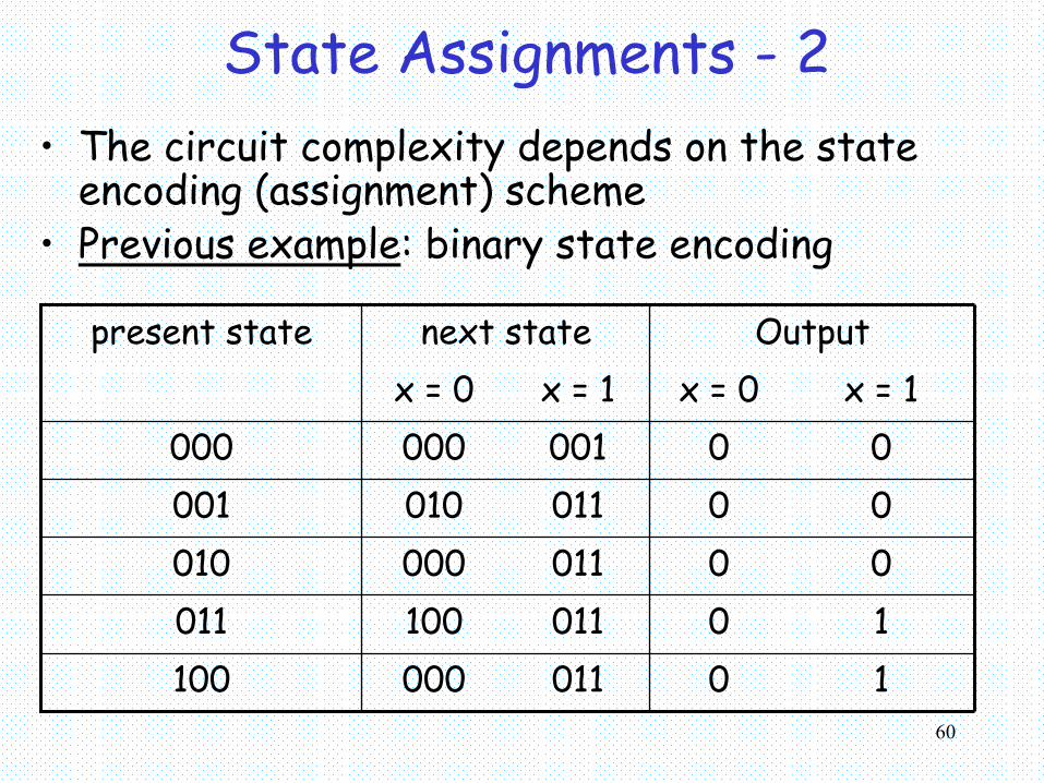
State Assignments - 2• The circuit complexity depends on the state
encoding (assignment) scheme• Previous example: binary state encoding
1001100010010011100011000110000100001101000100001000000
x = 1x = 0x = 1x = 0Outputnext statepresent state
61
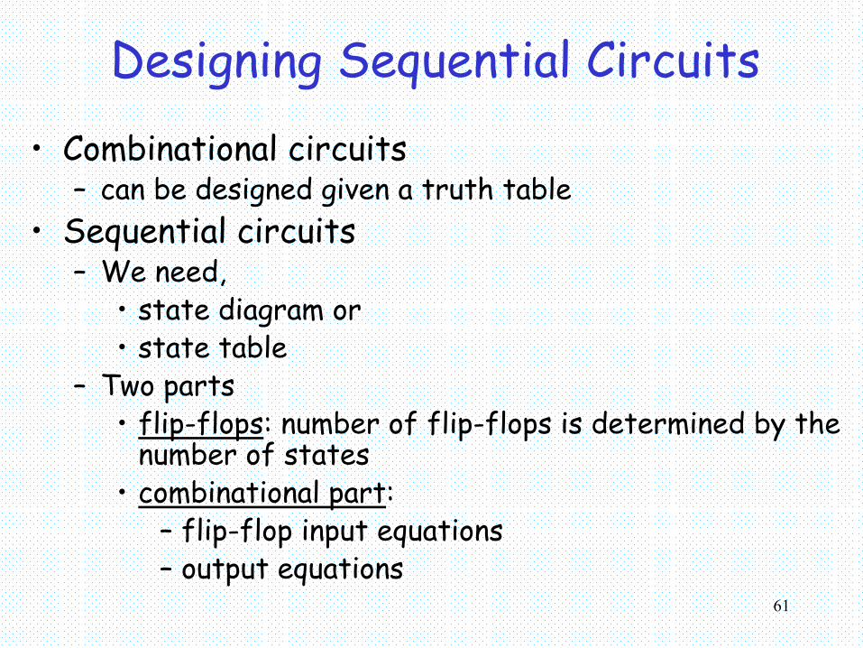
Designing Sequential Circuits• Combinational circuits
– can be designed given a truth table• Sequential circuits
– We need,• state diagram or• state table
– Two parts• flip-flops: number of flip-flops is determined by the
number of states• combinational part:
– flip-flop input equations– output equations
62
Design Process• Once we know the types and number of flip-
flops, design process is reduced to design process of combinational circuits
• Therefore, we can apply the techniques of combinational circuit design
• The design steps1. Given a verbal description of desired operation,
derive state diagram2. Reduce the number of states if necessary and
possible3. State assignment
63
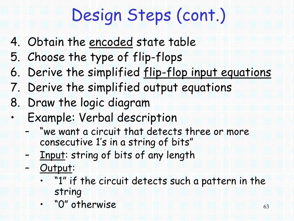
Design Steps (cont.)4. Obtain the encoded state table5. Choose the type of flip-flops6. Derive the simplified flip-flop input equations7. Derive the simplified output equations8. Draw the logic diagram• Example: Verbal description
– “we want a circuit that detects three or more consecutive 1’s in a string of bits”
– Input: string of bits of any length– Output:
• “1” if the circuit detects such a pattern in the string
• “0” otherwise
64
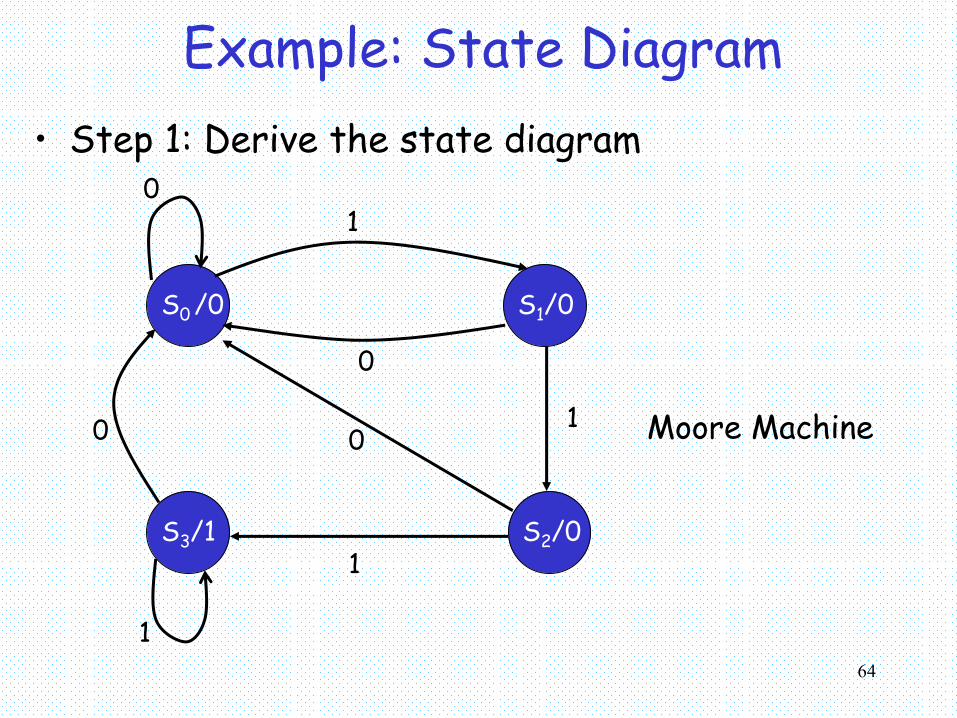
Example: State Diagram• Step 1: Derive the state diagram
S0 /0 S1/0
S2/0S3/1
01
0
10
1
1
0 Moore Machine
65
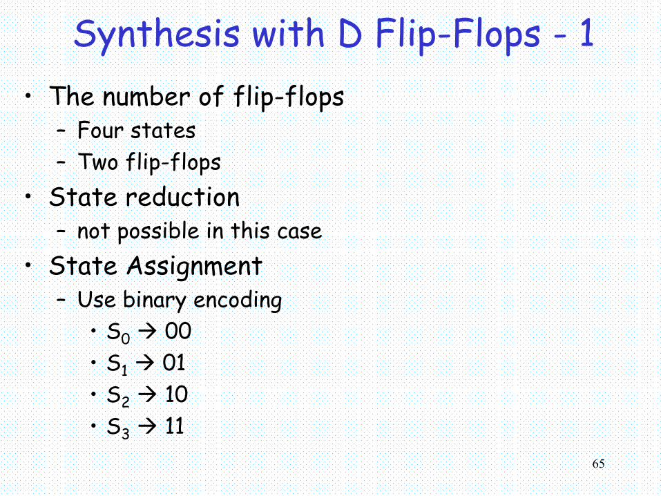
Synthesis with D Flip-Flops - 1• The number of flip-flops
– Four states– Two flip-flops
• State reduction– not possible in this case
• State Assignment– Use binary encoding
• S0 00• S1 01• S2 10• S3 11
66
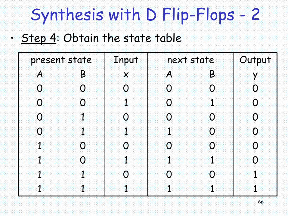
Synthesis with D Flip-Flops - 2• Step 4: Obtain the state table
111100011000001000010000
111011101001110010100000
yBAxBAOutputnext stateInputpresent state
67
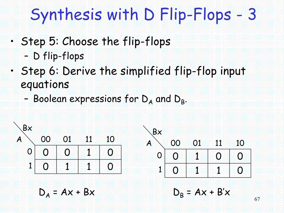
Synthesis with D Flip-Flops - 3• Step 5: Choose the flip-flops
– D flip-flops• Step 6: Derive the simplified flip-flop input
equations– Boolean expressions for DA and DB.
011010100010110100
BxA
DA = Ax + Bx
011010010010110100
BxA
DB = Ax + B’x
68
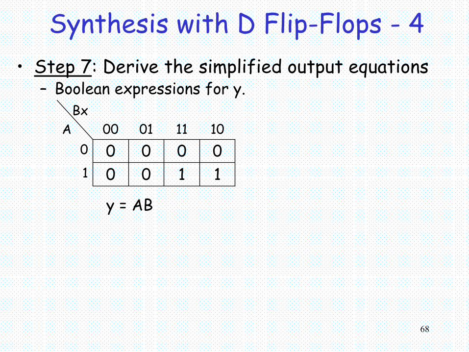
Synthesis with D Flip-Flops - 4• Step 7: Derive the simplified output equations
– Boolean expressions for y.
110010000010110100
BxA
y = AB
69
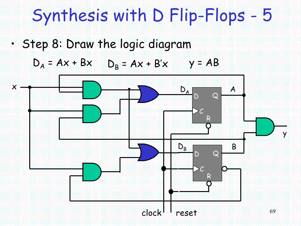
Synthesis with D Flip-Flops - 5• Step 8: Draw the logic diagram
DA = Ax + Bx DB = Ax + B’x y = AB
D Q
CR
D Q
CR
A
B
y
DA
DB
x
clock reset
70
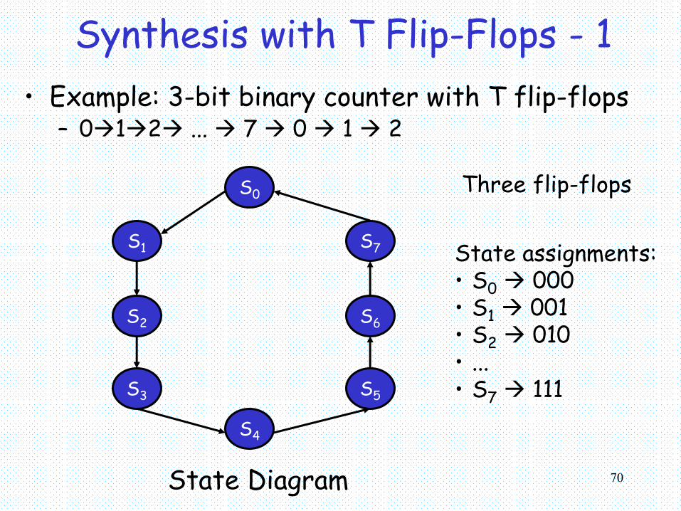
Synthesis with T Flip-Flops - 1• Example: 3-bit binary counter with T flip-flops
– 0 1 2 ... 7 0 1 2
S0
S1 S7
S2 S6
S3 S5
S4
Three flip-flops
State assignments:• S0 000• S1 001• S2 010• ...• S7 111
State Diagram
71
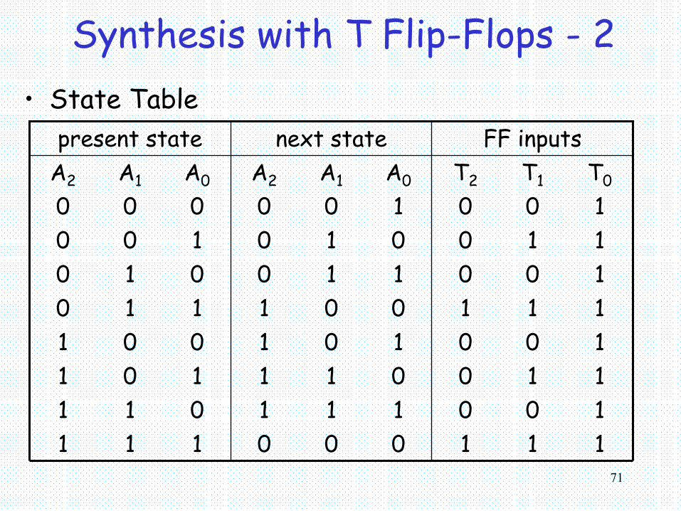
Synthesis with T Flip-Flops - 2• State Table
1000100
000111011101001110010
11111111
101010100100
111011101001110010100000
T0T1T2A0A1A2A0A1A2
FF inputsnext statepresent state
72
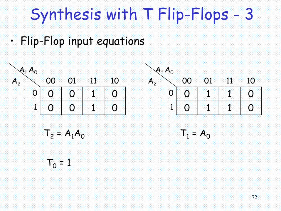
Synthesis with T Flip-Flops - 3• Flip-Flop input equations
010010100010110100
A1 A0
A2
T2 = A1A0
011010110010110100
A1 A0
A2
T1 = A0
T0 = 1
73
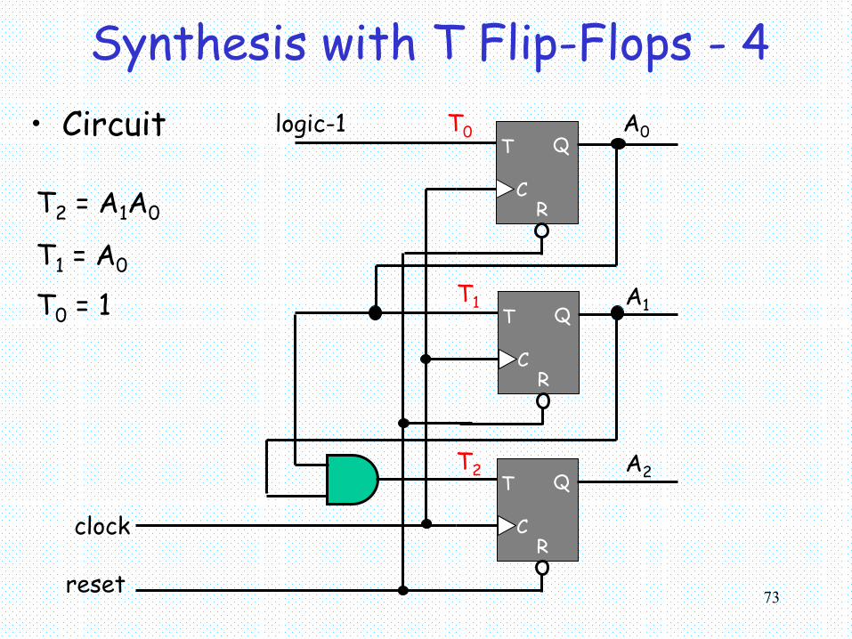
Synthesis with T Flip-Flops - 4• Circuit
T2 = A1A0
T1 = A0
T0 = 1
A0T Q
CR
T Q
CR
T Q
CR
A1
A2
logic-1 T0
T1
T2
clock
reset
74
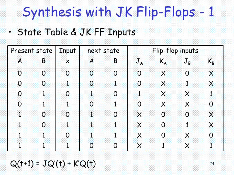
Synthesis with JK Flip-Flops - 1• State Table & JK FF Inputs
1X0X0X0XX0X1X0
1X0XX1X00X1XX1X0X0
0011111011111010100110110010101010000000
KBJBKAJABAxBAFlip-flop inputsnext stateInputPresent state
Q(t+1) = JQ’(t) + K’Q(t)
75
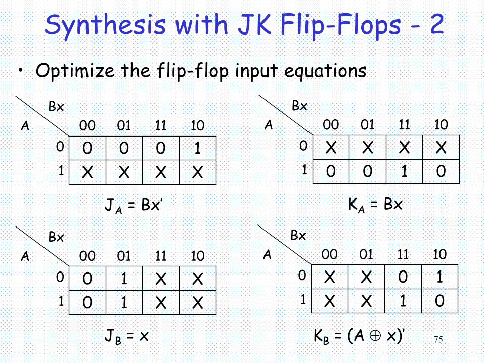
Synthesis with JK Flip-Flops - 2• Optimize the flip-flop input equations
XXXX11000010110100
BxA
JA = Bx’
01001XXXX010110100
BxA
KA = Bx
XX101XX10010110100
BxA
JB = x
01XX110XX010110100
BxA
KB = (A ⊕ x)’
76
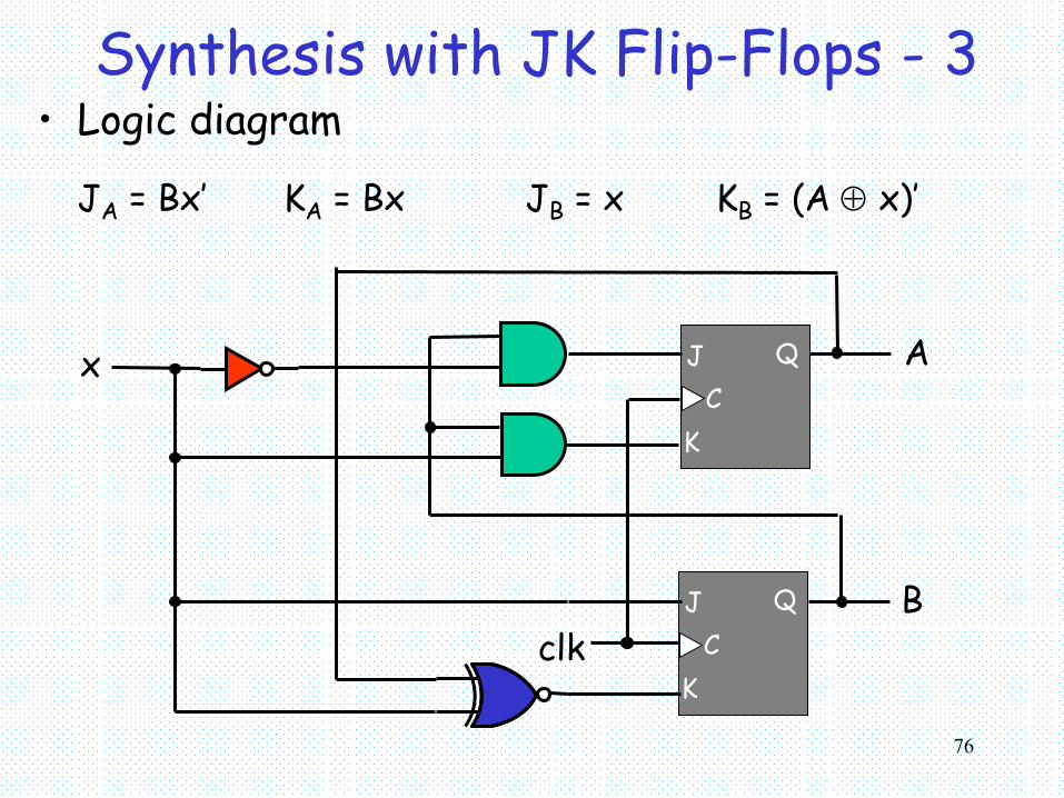
Synthesis with JK Flip-Flops - 3• Logic diagram
JA = Bx’ KA = Bx JB = x KB = (A ⊕ x)’
D Q
x
C
J QC
A
B
K
J QC
Kclk
77
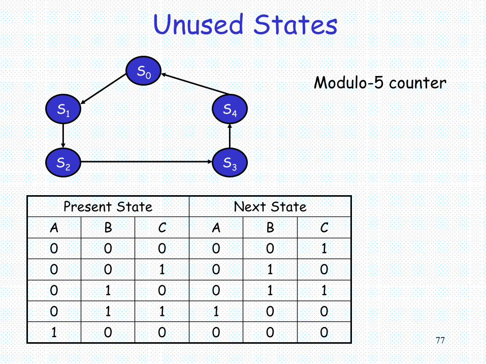
Unused StatesS0
S1
S2 S3
S4
Modulo-5 counter
001110000001
110010010100100000CBACBA
Next StatePresent State
78
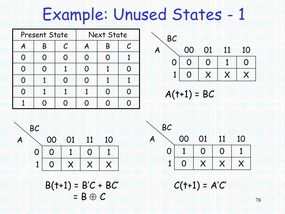
Example: Unused States - 1
001110000001
110010010100100000CBACBA
Next StatePresent State
XXX010100010110100
BCA
A(t+1) = BC
XXX0110100
10110100BC
A
B(t+1) = B’C + BC’= B ⊕ C
XXX0110010
10110100BC
A
C(t+1) = A’C’
79
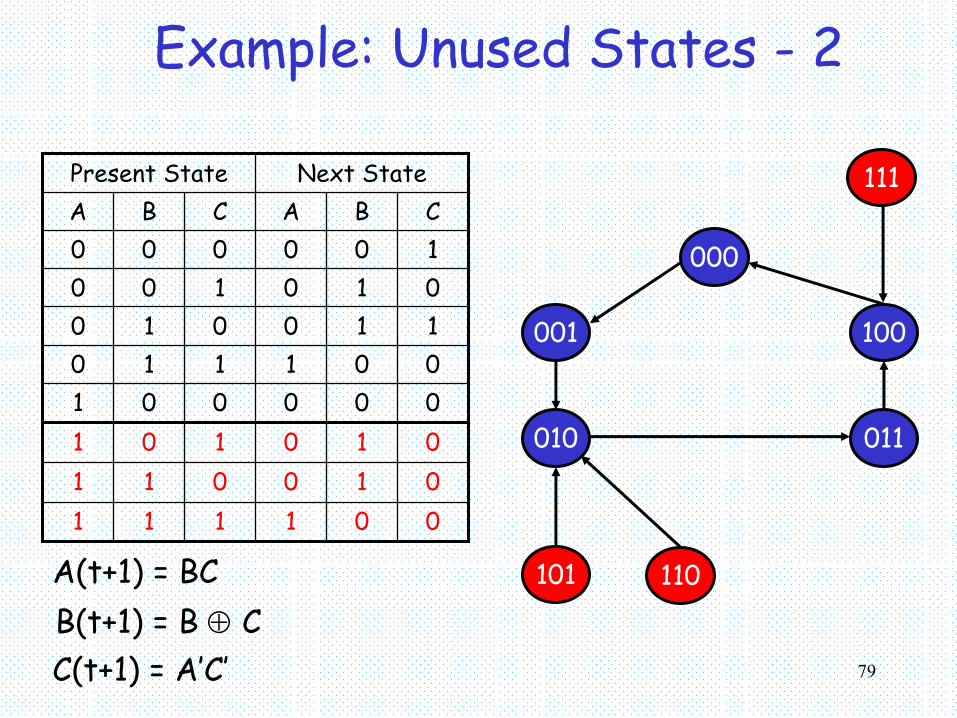
Example: Unused States - 2
010011010101000001001110
001111
110010010100100000CBACBA
Next StatePresent State
A(t+1) = BCB(t+1) = B ⊕ CC(t+1) = A’C’
000
001
010 011
100
101 110
111
80
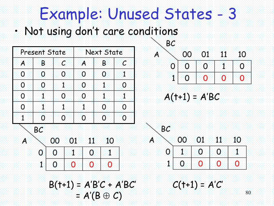
Example: Unused States - 3• Not using don’t care conditions
001110000001
110010010100100000CBACBA
Next StatePresent State
000010100010110100
BCA
A(t+1) = A’BC
0000110100
10110100BC
A
B(t+1) = A’B’C + A’BC’= A’(B ⊕ C)
0000110010
10110100BC
A
C(t+1) = A’C’
81
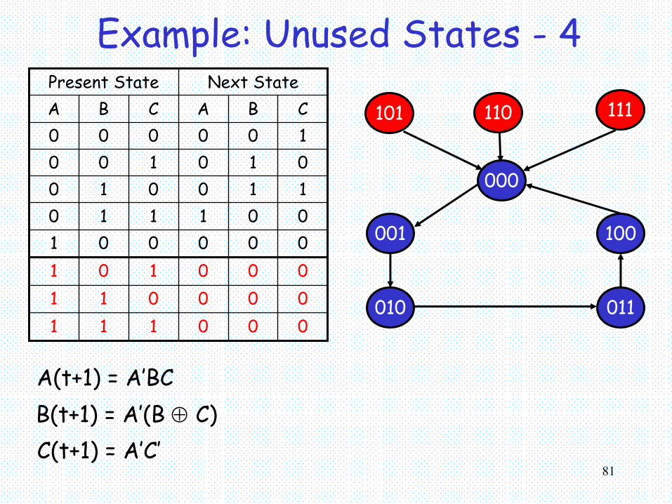
Example: Unused States - 4
000011000101000001001110
000111
110010010100100000CBACBA
Next StatePresent State
A(t+1) = A’BCB(t+1) = A’(B ⊕ C)C(t+1) = A’C’
000
001
010 011
100
101 110 111
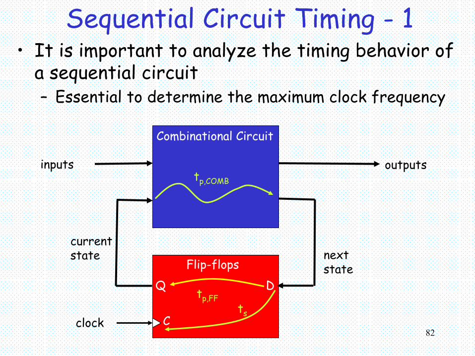
82clock
inputs outputs
currentstate next
state
Combinational Circuit
Flip-flopsDQ
C
Sequential Circuit Timing - 1• It is important to analyze the timing behavior of
a sequential circuit– Essential to determine the maximum clock frequency
ts
tp,COMB
tp,FF
83
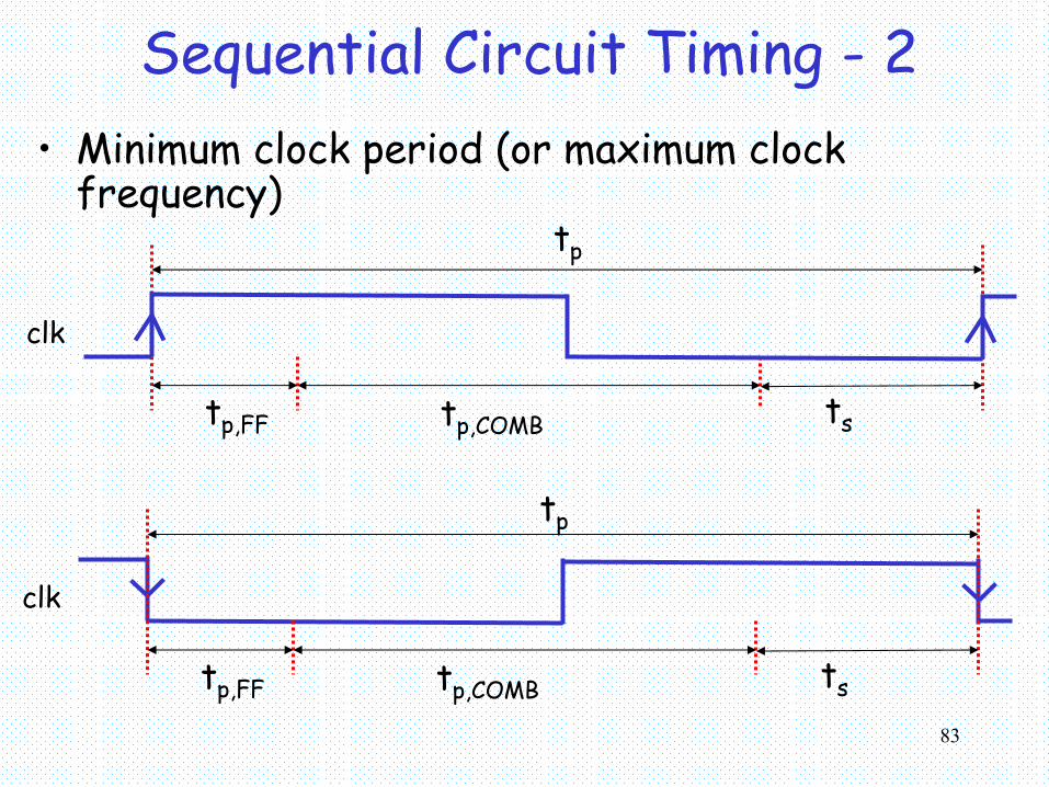
Sequential Circuit Timing - 2• Minimum clock period (or maximum clock
frequency)tp
tp,FF tp,COMB ts
clk
tp,FF tp,COMB ts
tp
clk
84
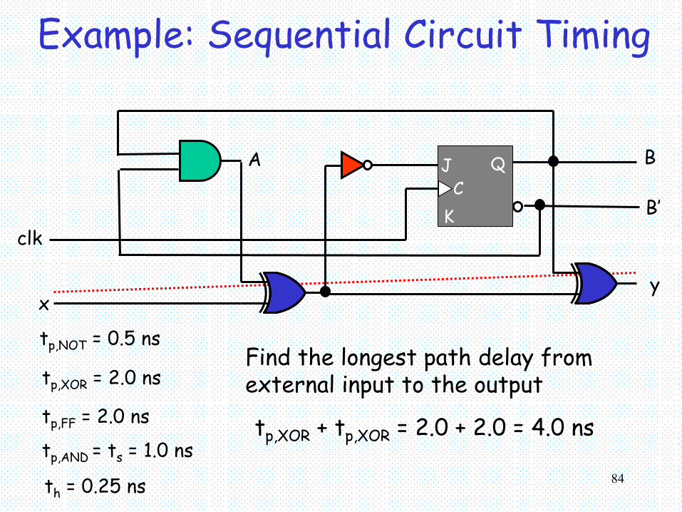
Example: Sequential Circuit Timing
Find the longest path delay fromexternal input to the output
tp,XOR + tp,XOR = 2.0 + 2.0 = 4.0 ns
tp,NOT = 0.5 ns
tp,XOR = 2.0 ns
tp,AND = ts = 1.0 ns
th = 0.25 ns
tp,FF = 2.0 ns
J QC
K
B
xy
A
B’clk
85
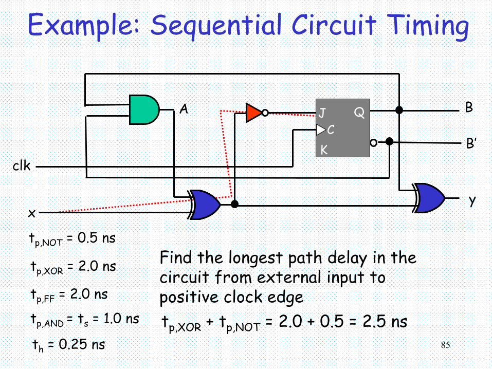
Example: Sequential Circuit Timing
Find the longest path delay in the circuit from external input to positive clock edgetp,XOR + tp,NOT = 2.0 + 0.5 = 2.5 ns
tp,NOT = 0.5 ns
tp,XOR = 2.0 ns
tp,AND = ts = 1.0 ns
th = 0.25 ns
tp,FF = 2.0 ns
J QC
K
B
xy
A
B’clk
86
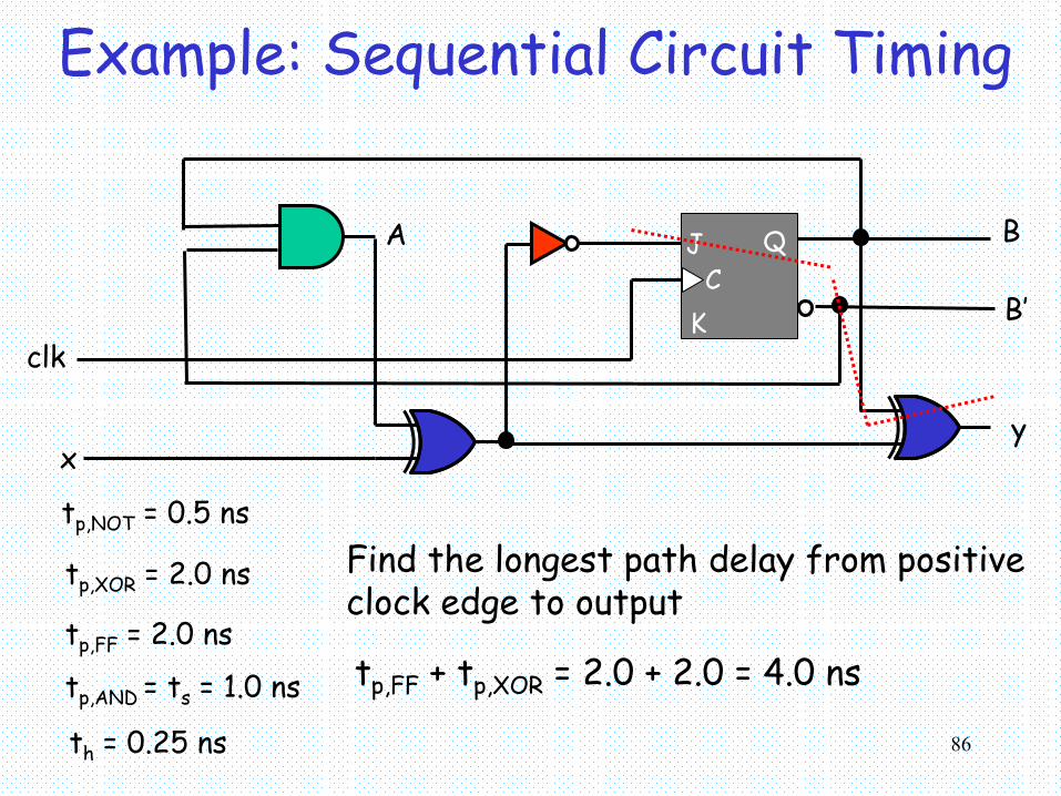
Example: Sequential Circuit Timing
Find the longest path delay from positive clock edge to output
tp,FF + tp,XOR = 2.0 + 2.0 = 4.0 ns
tp,NOT = 0.5 ns
tp,XOR = 2.0 ns
tp,AND = ts = 1.0 ns
th = 0.25 ns
tp,FF = 2.0 ns
J QC
K
B
xy
A
B’clk
87
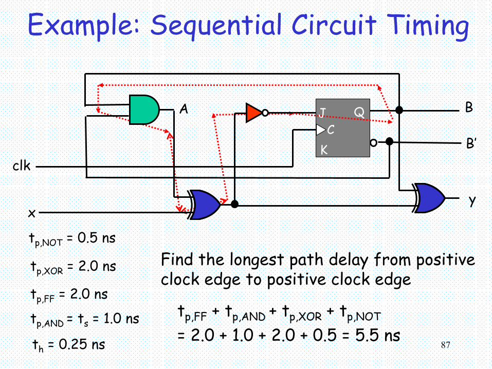
Example: Sequential Circuit Timing
Find the longest path delay from positive clock edge to positive clock edge
tp,FF + tp,AND + tp,XOR + tp,NOT
= 2.0 + 1.0 + 2.0 + 0.5 = 5.5 ns
tp,NOT = 0.5 ns
tp,XOR = 2.0 ns
tp,AND = ts = 1.0 ns
th = 0.25 ns
tp,FF = 2.0 ns
J QC
K
B
xy
A
B’clk
88
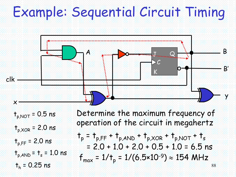
Example: Sequential Circuit Timing
Determine the maximum frequency of operation of the circuit in megahertztp = tp,FF + tp,AND + tp,XOR + tp,NOT + ts
= 2.0 + 1.0 + 2.0 + 0.5 + 1.0 = 6.5 nsfmax = 1/tp = 1/(6.5×10-9) ≈ 154 MHz
tp,NOT = 0.5 ns
tp,XOR = 2.0 ns
tp,AND = ts = 1.0 ns
th = 0.25 ns
tp,FF = 2.0 ns
J QC
K
B
xy
A
B’clk