Embed Size (px)
Citation preview
1
Low-cost direct writing lithography system for the sub-micron range
Holger Becker, Reinhard Caspary, Christian Toepfer, Manfred v. Schickfus, Siegfried
Hunklinger
Institut für Angewandte Physik, Universität Heidelberg, Albert Überle Str. 3-5, D-69120 Hei-
delberg, Germany
Abstract: We have developed a fixed beam direct writing laser lithography system with a
resolution of 400 nm at 457 nm wavelength and a writing speed of 4.2 mm/s with total
system costs of less than 100 000 US$.
Keyword: Laser lithography system
1. Introduction
Although research into lithographic systems in the past few years has mainly been carried out
in semiconductor industry due to its enormous economic potential, the possibilites of
structuring surfaces or producing photolithographic masks at micron or sub-micron range is
highly sought after in many fields of physics or chemical physics. The high costs of
commercially available lithography systems nevertheless restricts the access to this research
instrument. Therefore, we have realized a lithography system for such research activities
which is affordable even for small university budgets. It is designed for high flexibility and
frequent changes in mask design. Preference was given to a fast process from CAD mask
design to the finished photomask instead of high throughput of one specific mask pattern. The
maximum resolution of the system reaches 400 nm at a laser wavelength of 457 nm.
Optionally, the system can be equipped with a second-harmonic-generating extra cavity
BBO-crystal to provide a cw-DUV beam at 257 nm. The writing speed is limited to 4.2 mm/s
by the mechanical properties of the x-y-stage carrying the substrate, the exposure time for a
15×15 mm pattern is of the order of 13 hours.
2. Experimental setup
The experimental setup is shown in Fig. 1. The laser source is a Coherent Innova Argon ion
laser with a maximum power of 3 W at 514 nm and 300 mW at 457 nm. This high power
output can be used for a second harmonic generation, while typical beam power required for
the exposure of color-center masks [1] is of the order 100 mW. An electro-optical modulator
is used for switching the beam according to the pixel information. Typical pixel rates are
50 kHz. A prism deflects the beam via a dielectric mirror through a microscope lens (Leitz

2
100/0.95 for direct writing in photoresist, Planapo 25/0.65 for the exposure of color-center
masks) onto the substrate. If a BBO-crystal is installed, the prism discriminates the fun-
damental beam from its second harmonic. This fixed beam setup was chosen in order to
maximize optical resolution. We can illuminate the full numerical aperture of the microscope
lens in contrast to lithographic systems which sweep the beam across the aperture [2]. The
lithographic pattern is generated by moving the substrate on an x-y-stage (Jakob TLC 4S)
with DC servo motors. Areas which are to be exposed are scanned line by line in a
bidirectional manner, different areas can be successively processed in a pseudo vector mode,
where the starting coordinates of the pattern can be directly adressed. The position
information is obtained by a laser interferometer (Hewlett Packard 5501 A). The maximum
scan area is 90×90 mm. The pixel size is currently set to 80×40 nm in x- and y-direction, but
can easily be changed in steps of factor two. The y-distance of two successive lines of
exposure is set to 400 nm.
2.1 Electronics
A diagram of the electronic setup is shown in Fig. 2. The position information is delivered
from the interferometer in form of 180 ns pulses every 79.1 nm (= λ/8 of the interferometer
wavelength) in x-direction or 39.6 nm in y-direction (= λ/16). These pulses are collected in
two 32 bit (8 times 4 bit) up/down counters, which are read out by a 486DX2 personal
computer. The counter readings are used to direct the x-y stage to any desired position. While
exposing a pattern, the x-pulses of the interferometer enter the central element of the
exposure electronics, the "turning-counter". This counter has two modes of operation. The
first mode, the exposure mode, is used while exposing a line of the pattern. The computer
delivers the pixel data 8 bit asynchronously to a parallel-serial converter (PSC), which drives
the electro-optical modulator. The turning counter provides a data shift clock signal to the
PSC, which is synchronised to the interferometer pulses. Therefore the pixel data reach the
correct position on the substrate independent from the actual velocity of the x-y-stage. The
turning-counter also compensates position error induced by rocking or vibration of the stage
in x-direction. After the last bit of a particular line has been sent to the modulator, an end-of-
line signal is delivered to the turning-counter. This signal starts the second mode, the turning
mode. In this mode, the output to the modulator is blocked. All incoming position pulses in x-
direction are counted internally with a 20 bit up/down counter, starting with a reading of 0 at
the end-of-line signal. This counter records the position of the stage while decelerating,
moving into the next pattern line and accelerating into the reverse direction. If the counter has
reached a reading of 0 again, it switches automatically back into the exposure mode. The
displacement in y-direction from one line to the next is governed by a closed loop control,
which compares the actual position with the target position and stops the y-motor on arriving.
3
2.2 The y-direction correction stage
Even with a high precision x-y-stage there is some deviation in y-direction while moving the
stage in x-direction. This so-called "run-out", caused by imperfections of the guiding rails and
typically of the order of micrometer, has to be compensated in order to achieve straight lines
in the submicron range. We have realized a compensation with an additional stage on top of
the x-y-stage. This correction stage is shown in Fig. 3. At the beginning of each line the y-
count is used as reference value of an open loop circuit. During the scan of a line, any
deviation from this value is detected by the interferometer and counted in a seperate unit. The
counter reading is then AD-converted into a correction signal, which drives a linear piezo
element (Physik Instrumente P244-20) with range of ±10 µm to compensate the measured
deviation. The piezo element is equipped with an internal position sensor to eliminate
hysteresis effects.
2.3 Autofocus system
In order to maintain a constant distance between substrate and microscope lens, the lithograph
is equipped with an autofocus system. It is taken as a whole from a Phillips CD-player. The
beam of an IR-laser diode is coupled into the light path of the exposing beam. It is reflected
from the substrate and detected in a sectored diode. As its focal shape changes with the z-
position of the microscope lens, a distance dependent voltage is returned from the diode. This
signal is then used as input value to a closed loop circuit which adjusts the position of the
microscope lens by driving a piezo translator (Physik Instrumente PIFOC 720). Typical
resolution in z-direction is of the order of 100 nm. For a coarse adjustment the complete lens
unit is mounted on a stage which can be moved by stepper motors in steps of 10 µm.
2.4 Software
In order to have a high degree of flexibility in mask design and easy handling, the input data are
obtained from a commercially available CAD program (EASYCAD by EVOLUTION). Sup-
ported patterns are arbitrary polygons and text. Alternatively, files in Autocad DXF and TIFF
format can be exposed. These design data are then compressed in a three step process, as
complex designs can easily reach several megabyte of data. Pure pixel data would even reach
the gigabyte range and are therefore impossible to process or transport. The first compression
step is a run-length encoding, these length codes are then Huffman compressed [3] and finally
packed with a modified Lempel-Ziv-Welch compressor [4]. Typical size ratios between the
pure pixel data, the CAD data and the packed data are 2500:10:1. The pixel data for one scan
line are retrieved from the packed format during the turning of the x-y stage at the end of each
line within some ten milliseconds on a 486DX2 personal computer. The complete control
program is written in Turbo Pascal 6.0 and contains 5200 lines of code.

4
3. Experimental results
For most practical applications which do not require maximum resolution, patterns were
exposed into color center photomask blanks from Canyon Materials [1]. The mask blank
contains a 3 µm thick layer of color centers in a crown-glass matrix which absorbs light from
the UV to the IR region and hence appears black. By locally heating this layer to temperatures
above 300°C, the color centers are bleached, the mask becomes transparent. For a writing
speed between 7 and 9 mm/s a laser output of 90 mW is necessary to induce this process. This
corresponds to an energy density of 900 J/cm2 with a focal diameter of 1.4 µm. In Fig. 4, a
section of mask used for the production of surface acoustic wave devices is shown. The size
of the electrode fingers is 4 µm, the complete pattern is 10 mm×15 mm. As no more process
steps like developing, etching etc. are necessary with these masks, they can be used directly
after exposure in the lithographic system.
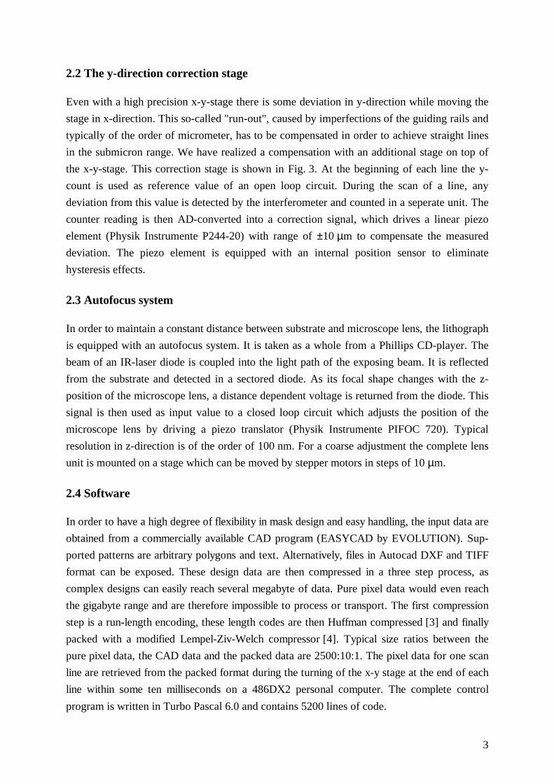
In Fig. 5, a test pattern written in 500 nm AZ 1350 resist is shown. These patterns were
obtained by widening the laser beam with a telescope to the full aperture of the microscope
lens in order to obtain maximum optical resolution.
Figure 6 shows a grating for STM calibration measurements. It consists of 1 µm lines and
spaces in x and y direction. The effect of two different sizes of the resist islands results from
the selected step size of 400 nm in y-direction, which leads to islands which are either two or
three pixels wide (800 or 1200 nm).
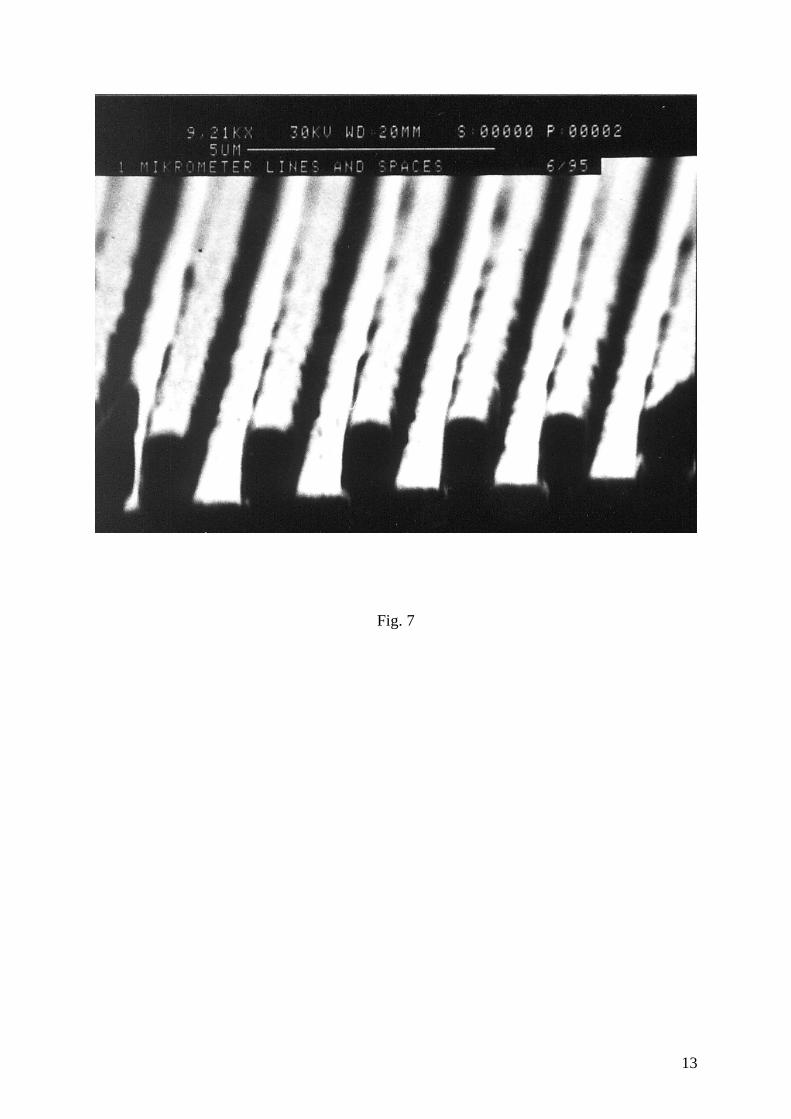
Figure 7 shows 1 µm lines and spaces in x direction. The edge roughness indicates the limits
of the mechanical compensation stage, which is well below 100 nm.
4. System costs
In Table 1, an overview on the different components of the system and their approximate
price is given. A considerable reduction in cost can be archieved in dispensing with the UV-
option. In this case, a much less powerful laser is needed and air-cooled HeCd-lasers can be
used.

5
Table 1. The costs of the system components used.
Component approx. price in US$
Ar Ion Laser 40 000
Interferometer 30 000
x-y stage, motors and electronics 10 000
y correction stage with electronics 4 000
electo-optical modulator, prism, lenses and
mirrors
6 000
autofocus system and z-piezo 2 500
Computer and interface cards 3 000
optional: BBO-crystal
UV microscope lens
6 000
15 000
5. Summary
We have presented a low-cost direct writing laser lithography system. Its main feature is a
fixed optical beam, the exposure pattern is generated by scanning the substrate on an x-y-
stage. The position error during exposure is compensated with a piezo-driven y-correction
stage. The system is designed for short cycle times from mask design with a CAD program to
the finished lithographic mask. Test patterns reveal an optical resolution of 400 nm in 500 nm
thick AZ-1350 photoresist. With this system all masks necessary for the production of surface
acoustic wave devices [5] have been produced.
6. References
1. Canyon Materials, San Diego, California: Product information on CM 200 photomask
blanks.
2. R.W.Wijnaendts-van-Resandt, C. Buchner: "Super Resolution Lithography using a Direct
Write Laser Pattern Gernerator", in Nanofabrication Technologies and Device Integration,
W.Karte, ed. (Proc. SPIE 2213, 1984), pp. 18-23.
3. R. Sedgewick, Algorithms (Addison-Wesley, Reading, MA, 1984), chap. 22, pp. 283-293.
4. T.A.Welch: "A Technique for High Performance Data Compression", IEEE Computer, vol
17, no. 6 (1984).
5. H.Becker, M.v.Schickfus, S.Hunklinger: "A New Sensor Principle Based on the Reflection
of Surface Acoustic Waves", in Sensors and Actuators (Proceedings Transducers ´95,
Eurosensors IX, to be published).

6
Figure Captions
Fig. 1: Experimental setup of the laser scanner. The laser beam remains fixed, the pattern is
generated by moving the x-y stage.
Fig. 2: Block diagram of the electronic system. The turning counter obtains the position
information from the interferometer and controls the data output to the modulator.
Fig. 3: Concept of the y-correction stage. The position error of the substrate is compensated
by a controlled piezo translator.
Fig. 4: Section of a colorcenter mask for the production of surface acoustic wave devices. The
white areas are bleached by locally heating the mask with the laser to 300°C. The electrode
width is 4 µm.
Fig. 5: Test pattern written into 500 nm AZ 1350 photoresist. The smallest features are
400 nm.
Fig. 6: Test structure for STM measurements. For details see text.
Fig. 7: 1 µm lines and spaces in 500 nm AZ 1350. The edge roughness shows the limits of the
y-compensation stage.

7
Fig. 1

8
Fig. 2

9
Fig. 3

10
Fig. 4
11
Fig. 5

12
Fig. 6
13
Fig. 7