Embed Size (px)
Citation preview
Low Cost Fiber Optic Links for Digital Applications up to 155 MBd
Application Bulletin 78
* Run length limited means a limit on the number of consecutive symbols in the same state.
** ST is a trademark of AT&T Technologies.
The HFBR-2406/16 High Performance Component
The HFBR-2406 and HFBR-2416 are high-speed, low-cost, linear, light-to-voltage converters with typical band-widths of 125 MHz. These components can be used to make fiber optic links for both analog and digital applica-tions. Since the range of possible uses is so varied, this application bulletin concentrates on a specific digital application. The application is one of the most prevalent for the HFBR-24X6: the transmission of encoded digital signals, otherwise known as run-length limited* data.
The HFBR-0400 component family’s inexpensive, one-piece plastic package allows engineers to construct low-cost high-performance fiber optic links. All devices in the HFBR-0400 product family, including the HFBR-24X6, are available with optical ports that are compat-ible with the industry standard SMA and ST** fiber optic connectors. Components that are compatible with the SMA connector are denoted by a “zero” in the third digit of their part numbers. If the ST connector is to be used, the component part number should contain a “one” in the third digit. For example, the equivalent of the high-performance HFBR-2406 SMA-compatible receiver with the ST connector option is the HFBR-2416.
The addition of the HFBR-24X6 receiver to the low-cost 0400 component family opens new avenues for designers. They can now develop fiber optic links that meet tough cost and performance objectives. The wide bandwidth of the HFBR-24X6 allows high-speed, fiber optic links to be built at lower prices than was formerly possible. Engi-neers can exploit the high performance of the HFBR-24X6 in other ways as well. For instance, the wide bandwidth of the linear light-to-voltage converter can be reduced by a low-pass filter to improve the sensitivity of the fiber optic receiver in lower-speed applications. The HFBR-24X6 accommodates a larger optical signal than other HFBR-0400 fiber optic receivers before it begins to over-load. This improvement in the overload characteristics of the 24X6 was achieved with no significant reduction in the ultimate sensitivity when compared to the existing HFBR-24X4 receiver. The increased optical input power
tolerated by the HFBR-24X6 allows it to function at short fiber lengths with large values of launched optical power. When the receiver can tolerate higher optical power, a longer cable is possible before attenuation reduces the light to the sensitivity limit of the receiver. The increased dynamic range of the HFBR-24X6 will thus permit greater optical link length for any given fiber attenuation.
Applications For 820 nm LED Based Fiber Optic Links
The 820-nm LED technology used in the HFBR-0400 family of components can be used in conjunction with the HFBR-24X6 receiver to construct digital fiber optic links that transmit data at speeds up to 155 MBd. The length of the fiber cable that can be used with the HFBR-24X6 is restricted by the receiver sensitivity at low data rates. As the data rate is increased a phenomenon known as chromatic dispersion begins to limit the maximum dis-tance. Chromatic dispersion results from the interaction of the 60 nm-wide spectrum emitted by the LED and the propagation velocities of light in silica. Since the velocities of light at various wavelengths near 820 nm are different, the optical pulses sent by the LED are dispersed or spread out in time as they travel down the light guide. A chromatic dispersion null exists at a wave-length of 1300 nm in silica glass. If an LED were operated at the chromatic dispersion null the pulses would experi-ence the minimum broadening as they traveled through the fiber. This is due to the nearly equal propagation velocity for all the wavelengths transmitted through the silica light guide by the long-wavelength emitter. Figure 1 illustrates the effect of the LED center wavelength and spectral width on the chromatic dispersion. An 820 nm LED with a 60 nm emission spectrum is shown to pro-duce a larger change in the arrival time of the light pulses than a 1300 nm LED with a 100 nm spectral width. When selecting a fiber the designer should be aware of how the bandwidth-length product, expressed in MHz/km, was determined. The bandwidth of a fiber measured us-ing a narrow spectrum emitter, such as a laser diode, is
2
Figure 1. Group Delay vs. Wavelength.
related to the various possible modes of light propa-gation that can exist in a fiber. This is referred to as the fiber’s modal bandwidth. The modal bandwidth will be greater than the chromatic bandwidth which dominates when an LED is used. To determine the overall optical bandwidth of a fiber, the modal and chromatic band-widths must be combined as an rms sum as shown in Equation 1. In LED-based systems the wavelength, spec-tral width and response time of the emitter used as the fiber optic transmitter will affect the final system band-width. Thus, to understand how a fiber will work with an LED, one must know the type of optical source used to measure the manufacturer’s stated bandwidth. Avago HFBR-AWSyyy 100/140 µm fiber optic cable has a typi-cal optical bandwidth-length product of 40 MHz/km. This value represents the performance of the Avago fiber with an 820 nm LED emitter that has a 60 nm spectral width. The 40 MHz/km typical bandwidth-length product of
Avago fiber results from the combination of the modal and chromatic bandwidths.
The typical distances and data rates possible with 820 nm LED emitters and the HFBR-2406/2416 receiver are shown in Figure 2. Note that the data rate versus distance for 100/140 and 62.5/125 µm graded-index fibers are both shown in the figure.[1, 2, 3, 4]
If greater distances or higher speeds are required, other options such as 1300 nm LEDs or laser diodes can meet these objectives. If the system requirements fall to the left of the curves shown in Figure 2 the design goals can be achieved using an 820 nm LED and the HFBR-24X6 for a substantially lower cost than pos-sible with these other technologies. The inexpensive 820 nm LED technology offers the designer a cost- effective solution sufficient for many short-distance applications at data rates in excess of 100 megabaud.
1.48
1.47
1.46
GR
OU
P R
EF
RA
CT
IVE
IND
EX
500 1000 1500 2000λ - WAVELENGTH - nm
820 nm
1300 nm
5357-1
B.W. modal
1( )2
B.W. chromatic
1( )2
+
1
B.W. =
1/2
N = The number of 74ACT gatesconnected in parallel.B = Is an empirically determinedconstant which establishes an optimum relationship between prebias and LED forward current.
(Vcc – VF) (1 + B)
IF ON
Ry =
Rx1 = 2B
Ry
Rx2 = –
( )
2B
Ry ( ) 3
N( )C =
2.5 ns
Rx1
N = Number of gates connected in parallel.B = Empirically determined constant for optimum relationship between prebias and LED forward current.
(Vcc – VF) (1 + B)
IF ON
R10 =
R8 =2B
R10
R9 = –2B
R10 3
N
C4 =2.5 × 10⁻⁹
R8
Recommend B = 3.97
Equation 1.
3
Figure 2. Typical Data Rate and Distance Possible with HFBR-2406/2416.
Applications for 820 nm LED Based Systems Using HFBR-2406/2416 Include:
• CPU to disc interface.
• CPU to monitor interface
• CPU to peripheral interface
• Optical data bus applications.
• Graphics workstation to host computer interface.
• Wide dynamic range, long distance, medium speed LAN applications.
• High-speed, point-to-point data links.
• Security, voltage isolation.
Advantages of Run Limited Code
Data is coded to prevent the digital information from remaining in one of the two possible logic states for an indefinite period of time. The coded data allows the fiber optic receiver to be AC coupled. Without encoding, the fiber optic receiver would have to detect DC levels to determine the proper logic state during long periods of inactivity, as when there is no change in the transmitted data. AC-coupled fiber optic receivers tend to be lower in cost, are much easier to design, and contain fewer com-ponents than their dc-coupled counterparts.
Direct coupling decreases the sensitivity of a fiber optic receiver since it allows the low-frequency flicker noise from the transistor amplifiers to be presented to the
comparator input. Any undesired signals coupled to the comparator will reduce the signal-to-noise ratio at this critical point in the circuit, and reduce sensitivity of the fiber optic receiver.
Another problem associated with direct-coupled receiv-ers is minimizing the accumulation of DC offset. With direct coupling, the gain stages multiply the effects of undesirable amplifier offsets and voltage drifts due to temperature changes, and apply them to the compara-tor. Increases in the DC offset applied to the comparator result in reduced sensitivity of the fiber optic receiver. The DC offset at the comparator can be referred to the optical input of the receiver by dividing by the receiver gain. This division refers the DC offset at the compara-tor to the receiver input where it appears as a change in optical power that must be exceeded before the receiver will switch states.
Another advantage of run-limited coding is related to timing recovery. If NRZ data were transmitted over a serial fiber optic link the data could be in the logic “1” or logic “0” state for an indefinite period of time. When NRZ data remains in a particular state no transitions occur and the fundamental frequency of the data is DC. This lack of power at the fundamental frequency of the data elimi-nates the reference signal needed by the timing recovery circuits required to clock the received information. If an optical link is to transmit NRZ data, a clock signal must be sent on a separate fiber optic link to synchronously detect the incoming serial data.
DATA RATE POSSIBLE WITHSELECTED HFBR-24X6
DATA RATE POSSIBLE WITH STANDARD HFBR-24X6
62.5/125 µm FIBEROPTIC LIGHTGUIDE
ADDED DISTANCEPOSSIBLE WITH LOW
PASS FILTERING
100/140 µmFIBER OPTICLIGHTGUIDE
1,000
100
10
DA
TA
RA
TE
- S
YM
BO
LS
/sec
- M
Bd
0.1 1.0 10l - LENGTH - km
5357-2
DATA RATE POSSIBLE WITHSELECTED HFBR-24X6
DATA RATE POSSIBLE WITH STANDARD HFBR-24X6
62.5/125 µm FIBEROPTIC LIGHTGUIDE
ADDED DISTANCEPOSSIBLE WITH LOW
PASS FILTERING
100/140 µmFIBER OPTICLIGHTGUIDE
1,000
100
10
DA
TA
RA
TE
- S
YM
BO
LS
/sec
- M
Bd
0.1 1.0 10
l - LENGTH - km
4
The particular run-length-limited code chosen must be considered carefully since it will affect the bandwidth re-quired by the serial communication channel. A complete discussion of all run-limited codes is beyond the scope of this publication. If you desire additional information regarding various coding schemes, there are numerous technical papers devoted to this specific topic.[5] Without becoming too involved in the complexity of encoding selection, a quick comparison will now be made between two commonly recognized approaches to this problem.
One of the most familiar run-limited codes is Manchester. Manchester is very popular since it can be encoded and decoded with relatively simple circuits. Manchester works well in ac-coupled systems since it has a 50% duty factor and two pulses or symbols for each bit transmitted. This simplifies the design and implementation of the timing recovery function since Manchester code has only two consecutive symbols without a transition, or a run limit of two. A drawback of Manchester is that two symbols must be sent for each data bit encoded, thus doubling the fundamental frequency that must pass through the information channel. Substitution codes have recently been made available in very large scale integrated (VLSI) circuits. These VLSI circuits function as a general purpose interface between the parallel architecture found in com-puter-based systems and the serial format required by fiber optic communication links. The two different sub-stitution codes available in the AMD TAXIchip™ parallel- to-serial encoder are 4B5B and 5B6B. These two codes have an efficiency of 4/5 and 5/6 respectively which compares to an efficiency of 1/2 for Manchester code. The significance of coding efficiency can be illustrated by an example. If an application calls for the transmission of 100 M bits/second, Manchester code requires that the information channel must pass 200 M symbols/second or 200 MBd. If the more efficient 4B5B code were used, 100 M bits/second could be sent at a speed of (5/4)(100 M bit/sec) = 125 MBd. Similarly, use of 5B6B would allow trans-mission of this data at a speed of (6/5)(100 M bit/sec) = 120 MBd.
Regardless of the particular coding scheme used there will always be two symbols per cycle. This is true because each half cycle of the maximum fundamental frequency that the communications channel must pass is equiva-lent to a symbol in a binary transmission system.
Designing With Fiber Optic Components
Transmitter Design
Now that the basic issues related to fiber optic link design have been covered, some specifics related to the design of the optical transmitters and receivers will be discussed in greater detail. To achieve the wide bandwidth perfor-mance potential of the fiber optic medium requires a fast LED and current modulator. The transmitter’s pulse-width distortion and optical rise and fall times can be heavily influenced by the driver selected. Readily avail-able off-the-shelf integrated circuit current drivers can be configured with the HFBR-14XX 820 nm LEDs to build high-performance fiber optic transmitters with a typical pulse-width distortion of 800 psec.
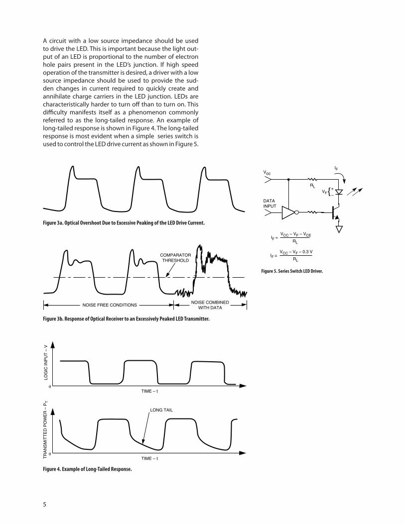
To obtain the best performance from any LED and driver combination, two simple techniques known as prebias and drive current peaking should be employed. Prebias, as its name implies, is a small forward current applied to the LED in the “off ” or “low” light state. The prebias cur-rent prevents the junction and parasitic capacitances from discharging completely when the LED is in the “off ” state, thus reducing the amount of charge that the driver must transfer to turn the emitter back on. Peaking is a momentary increase in LED forward current that is pro-vided by the driver during the rising and falling edges of the current pulses that are used to modulate the emitter. If the time constant of the peaking circuit is approxi-mately equal to the minority carrier lifetime of the emit-ter, the momentary increase in LED current will transfer charge at a rate that improves the rise or fall time of the light output without causing excessive overshoot of the optical pulses. Problems that can result when excessive peaking is applied to the LED are illustrated in Figure 3. The narrow optical overshoot due to excessive peaking of the transmitter causes a narrow electrical output pulse from the fiber optic receiver that must now be damped. Even if the receiver amplifiers were critically damped the electrical undershoot resulting from excessive peaking of the emitter can reduce the sensitivity of the fiber optic link. This electrical undershoot can combine with noise from the amplifiers so that the sum of these two voltages exceeds the decision threshold of the comparator, which converts the low-level analog output of the fiber optic receiver back to logic-compatible digital signals. Exces-sive peaking during the turn-off of the emitter can cause additional problems. Too much reverse current during the turn-off transition will reverse-bias the LED, seriously degrading the turn-on time.
5
A circuit with a low source impedance should be used to drive the LED. This is important because the light out-put of an LED is proportional to the number of electron hole pairs present in the LED’s junction. If high speed operation of the transmitter is desired, a driver with a low source impedance should be used to provide the sud-den changes in current required to quickly create and annihilate charge carriers in the LED junction. LEDs are characteristically harder to turn off than to turn on. This difficulty manifests itself as a phenomenon commonly referred to as the long-tailed response. An example of long-tailed response is shown in Figure 4. The long-tailed response is most evident when a simple series switch is used to control the LED drive current as shown in Figure 5.
Figure 4. Example of Long-Tailed Response.
Figure 5. Series Switch LED Driver.
Figure 3a. Optical Overshoot Due to Excessive Peaking of the LED Drive Current.
Figure 3b. Response of Optical Receiver to an Excessively Peaked LED Transmitter.
NOISE FREE CONDITIONSNOISE COMBINED
WITH DATA
COMPARATORTHRESHOLD
Figure 3a. Optical Overshoot Due to Excessive Peaking of the LED Drive Current.
Figure 3b. Response of Optical Receiver to an Excessively Peaked LEDTransmitter.
5357-3ab
NOISE FREE CONDITIONSNOISE COMBINED
WITH DATA
COMPARATORTHRESHOLD
Figure 3a. Optical Overshoot Due to Excessive Peaking of the LED Drive Current.
Figure 3b. Response of Optical Receiver to an Excessively Peaked LEDTransmitter.
5357-3ab
VccIF
VF
RL +
–DATAINPUT
VCC – VF – VCE
RLIF =
VCC – VF – 0.3 V
RLIF ≅
5357-5
TIME – t
TIME – t
LOG
IC IN
PU
T –
V
φ
TR
AN
SM
ITT
ED
PO
WE
R –
PT
φ
LONG TAIL
5357-4
6
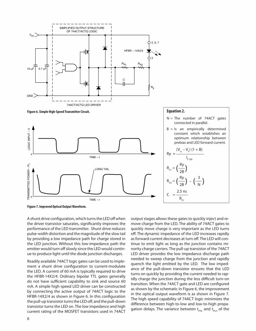
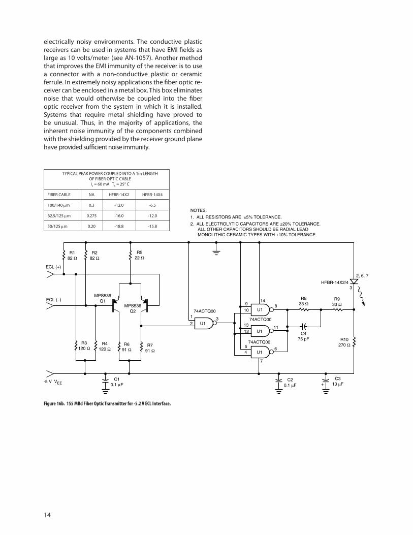
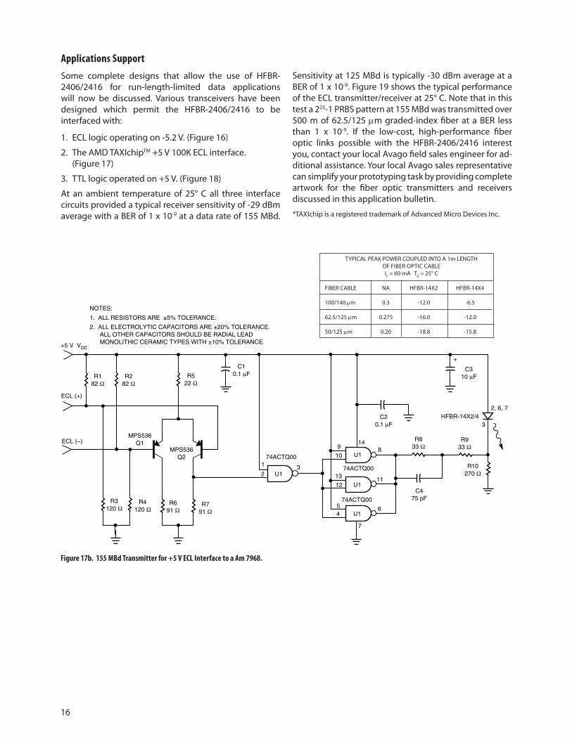
A shunt drive configuration, which turns the LED off when the driver transistor saturates, significantly improves the performance of the LED transmitter. Shunt drive reduces pulse-width distortion and the magnitude of the slow tail by providing a low impedance path for charge stored in the LED junction. Without this low-impedance path the emitter would turn off slowly since the LED would contin-ue to produce light until the diode junction discharges.
Readily available 74ACT logic gates can be used to imple-ment a shunt drive configuration to current-modulate the LED. A current of 60 mA is typically required to drive the HFBR-14X2/4. Ordinary bipolar TTL gates generally do not have sufficient capability to sink and source 60 mA. A simple high-speed LED driver can be constructed by connecting the active output of 74ACT logic to the HFBR-14X2/4 as shown in Figure 6. In this configuration the pull-up transistor turns the LED off, and the pull-down transistor turns the LED on. The low impedance and high current rating of the MOSFET transistors used in 74ACT
output stages allows these gates to quickly inject and re-move charge from the LED. The ability of 74ACT gates to quickly move charge is very important as the LED turns off. The dynamic impedance of the LED increases rapidly as forward current decreases at turn off. The LED will con-tinue to emit light as long as the junction contains mi-nority charge carriers. The pull-up transistor of the 74ACT LED driver provides the low impedance discharge path needed to sweep charge from the junction and rapidly quench the light emitted by the LED. The low imped-ance of the pull-down transistor ensures that the LED turns on quickly by providing the current needed to rap-idly charge the junction during the less difficult turn-on transition. When the 74ACT gate and LED are configured as shown by the schematic in Figure 6, the improvement in the optical output waveform is as shown in Figure 7. The high speed capability of 74ACT logic minimizes the difference between high-to-low and low-to-high propa-gation delays. The variance between t
PHL and t
PLH of the
Figure 6. Simple High-Speed Transmitter Circuit.
Figure 7. Improved Optical Output Waveform.
Equation 2.
N = The number of 74ACT gates connected in parallel.
B = Is an empirically determined constant which establishes an optimum relationship between prebias and LED forward current.
(Vcc
– VF) (1 + B)
Ry = I
F ON
RyR
X1 = ( )
2B
Ry 3R
X2 = ( ) – ( )
2B N
2.5 nsC =
R
X1
TIME – t
TIME – t
LOG
IC IN
PU
T –
V
φ
TR
AN
SM
ITT
ED
PO
WE
R –
PT
φ
LONG TAIL
5357-7
2, 6, 7
3
C
Rx1 Rx20.1 µF10 µF
HFBR – 14X2/4
Ry
Vcc
GND
SIMPLIFIED OUTPUT STRUCTUREOF 74ACT/ACTQ LOGIC
74ACT/ACTQ LED DRIVER
5357-6
7
Figure 9. Optical Output of the TTL Transmitter.
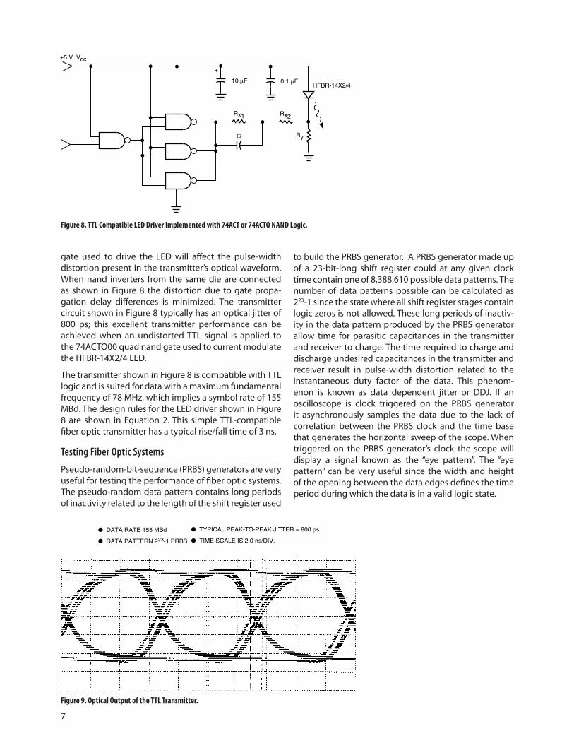
gate used to drive the LED will affect the pulse-width distortion present in the transmitter’s optical waveform. When nand inverters from the same die are connected as shown in Figure 8 the distortion due to gate propa-gation delay differences is minimized. The transmitter circuit shown in Figure 8 typically has an optical jitter of 800 ps; this excellent transmitter performance can be achieved when an undistorted TTL signal is applied to the 74ACTQ00 quad nand gate used to current modulate the HFBR-14X2/4 LED.
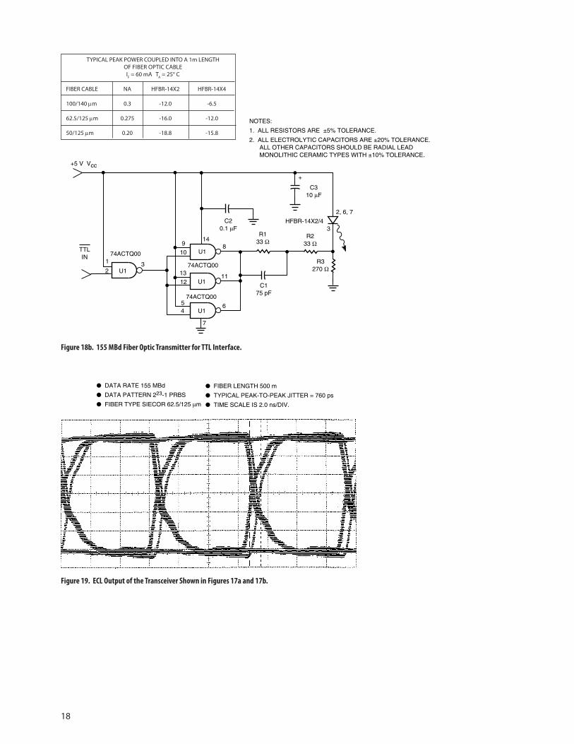
The transmitter shown in Figure 8 is compatible with TTL logic and is suited for data with a maximum fundamental frequency of 78 MHz, which implies a symbol rate of 155 MBd. The design rules for the LED driver shown in Figure 8 are shown in Equation 2. This simple TTL-compatible fiber optic transmitter has a typical rise/fall time of 3 ns.
Testing Fiber Optic Systems
Pseudo-random-bit-sequence (PRBS) generators are very useful for testing the performance of fiber optic systems. The pseudo-random data pattern contains long periods of inactivity related to the length of the shift register used
to build the PRBS generator. A PRBS generator made up of a 23-bit-long shift register could at any given clock time contain one of 8,388,610 possible data patterns. The number of data patterns possible can be calculated as 223-1 since the state where all shift register stages contain logic zeros is not allowed. These long periods of inactiv-ity in the data pattern produced by the PRBS generator allow time for parasitic capacitances in the transmitter and receiver to charge. The time required to charge and discharge undesired capacitances in the transmitter and receiver result in pulse-width distortion related to the instantaneous duty factor of the data. This phenom-enon is known as data dependent jitter or DDJ. If an oscilloscope is clock triggered on the PRBS generator it asynchronously samples the data due to the lack of correlation between the PRBS clock and the time base that generates the horizontal sweep of the scope. When triggered on the PRBS generator’s clock the scope will display a signal known as the “eye pattern”. The “eye pattern” can be very useful since the width and height of the opening between the data edges defines the time period during which the data is in a valid logic state.
Figure 8. TTL Compatible LED Driver Implemented with 74ACT or 74ACTQ nAnD Logic.
+5 V Vcc
C
Rx1
0.1 µFHFBR-14X2/4
5357-8
10 µF
Rx2
Ry
+
5357-9
TYPICAL PEAK-TO-PEAK JITTER = 800 ps
TIME SCALE IS 2.0 ns/DIV.
DATA RATE 155 MBd
DATA PATTERN 223-1 PRBS
8
Figure 11. Optical Output of the +5V ECL Transmitter.
Figure 10. Transmitter with +5V ECL Interface.
TTL Transmitter Performance
The performance of the circuit shown in Figure 8 was tested using a 223-1 PRBS data pattern to demonstrate the typical performance of this TTL transmitter. Jitter in the data edges results due to the DDJ induced by the pseudo random bit sequence. The eye pattern shown in Figure 9 reveals that the HFBR-14X2/14X4 LED trans-mitter had a total data-dependent edge jitter of 800 ps when driven by the 74ACTQ00 gate at a rate of 155 MBd. This data was taken at an ambient temperature of 25° C and represents the typical performance possible with this simple fiber optic transmitter. The total pulse-width distortion can be further reduced by using a limited-range potentiometer in place of fixed values of R
y for system applications that are extremely intolerant
of symbol-width variations. But for most data commu-nications applications, this transmitter performs ade-quately at speeds up to 155 MBd using fixed component values.
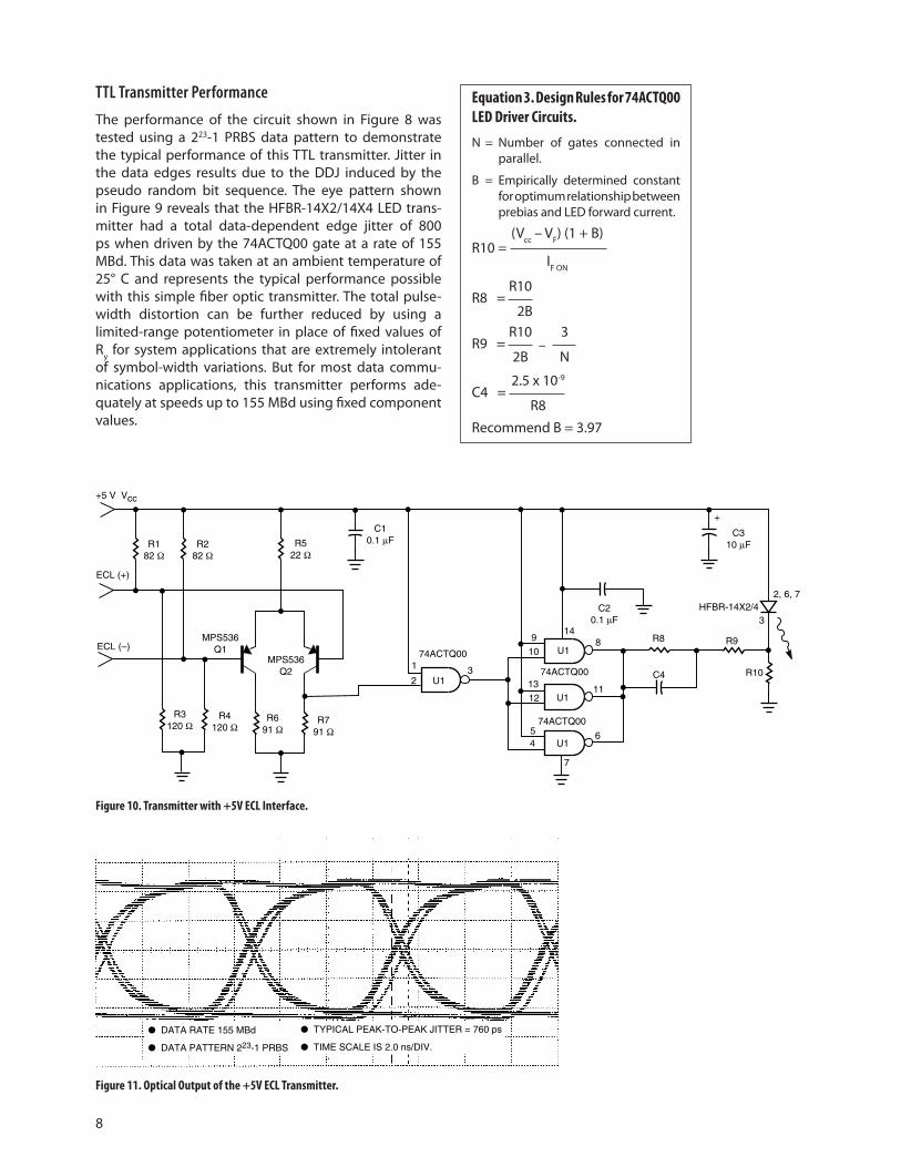
Equation 3. Design Rules for 74ACTQ00 LED Driver Circuits.
N = Number of gates connected in parallel.
B = Empirically determined constant for optimum relationship between prebias and LED forward current.
(Vcc
– VF) (1 + B)
R10 = I
F ON
R10R8 =
2B
R10 3R9 = –
2B N
2.5 x 10⁻⁹
C4 =
R8
Recommend B = 3.97
5357-11
TYPICAL PEAK-TO-PEAK JITTER = 760 ps
TIME SCALE IS 2.0 ns/DIV.
DATA RATE 155 MBd
DATA PATTERN 223-1 PRBS
R182 Ω
R282 Ω
R522 Ω
R3120 Ω
R4120 Ω
R691 Ω
R791 Ω
+5 V Vcc
ECL (+)
ECL (–)MPS536
Q1MPS536
Q2
C10.1 µF
74ACTQ001
23 74ACTQ00
74ACTQ00
U1
U1
U1
9
10
13
12
54
6
11
814
7
C4
R8 R9
R10
C20.1 µF
C310 µF
2, 6, 7
3
5357-10
U1
+
HFBR-14X2/4
9
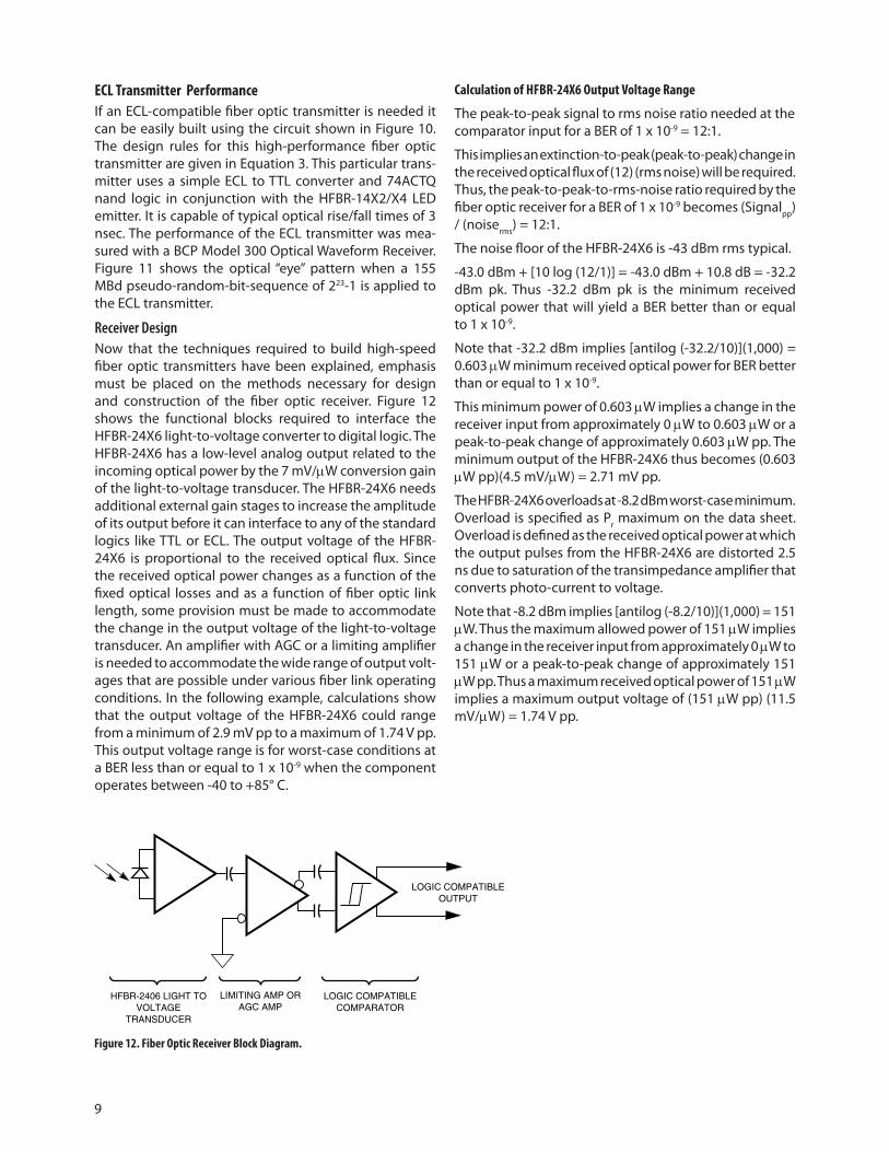
Figure 12. Fiber Optic Receiver Block Diagram.
Calculation of HFBR-24X6 Output Voltage Range
The peak-to-peak signal to rms noise ratio needed at the comparator input for a BER of 1 x 10-9 = 12:1.
This implies an extinction-to-peak (peak-to-peak) change in the received optical flux of (12) (rms noise) will be required. Thus, the peak-to-peak-to-rms-noise ratio required by the fiber optic receiver for a BER of 1 x 10⁻⁹ becomes (Signal
pp)
/ (noiserms
) = 12:1.
The noise floor of the HFBR-24X6 is -43 dBm rms typical.
-43.0 dBm + [10 log (12/1)] = -43.0 dBm + 10.8 dB = -32.2 dBm pk. Thus -32.2 dBm pk is the minimum received optical power that will yield a BER better than or equal to 1 x 10⁻⁹.
Note that -32.2 dBm implies [antilog (-32.2/10)](1,000) = 0.603 µW minimum received optical power for BER better than or equal to 1 x 10⁻⁹.
This minimum power of 0.603 µW implies a change in the receiver input from approximately 0 µW to 0.603 µW or a peak-to-peak change of approximately 0.603 µW pp. The minimum output of the HFBR-24X6 thus becomes (0.603 µW pp)(4.5 mV/µW) = 2.71 mV pp.
The HFBR-24X6 overloads at -8.2 dBm worst-case minimum. Overload is specified as P
r maximum on the data sheet.
Overload is defined as the received optical power at which the output pulses from the HFBR-24X6 are distorted 2.5 ns due to saturation of the transimpedance amplifier that converts photo-current to voltage.
Note that -8.2 dBm implies [antilog (-8.2/10)](1,000) = 151 µW. Thus the maximum allowed power of 151 µW implies a change in the receiver input from approximately 0 µW to 151 µW or a peak-to-peak change of approximately 151 µW pp. Thus a maximum received optical power of 151 µW implies a maximum output voltage of (151 µW pp) (11.5 mV/µW) = 1.74 V pp.
ECL Transmitter PerformanceIf an ECL-compatible fiber optic transmitter is needed it can be easily built using the circuit shown in Figure 10. The design rules for this high-performance fiber optic transmitter are given in Equation 3. This particular trans-mitter uses a simple ECL to TTL converter and 74ACTQ nand logic in conjunction with the HFBR-14X2/X4 LED emitter. It is capable of typical optical rise/fall times of 3 nsec. The performance of the ECL transmitter was mea-sured with a BCP Model 300 Optical Waveform Receiver. Figure 11 shows the optical “eye” pattern when a 155 MBd pseudo-random-bit-sequence of 223-1 is applied to the ECL transmitter.
Receiver DesignNow that the techniques required to build high-speed fiber optic transmitters have been explained, emphasis must be placed on the methods necessary for design and construction of the fiber optic receiver. Figure 12 shows the functional blocks required to interface the HFBR-24X6 light-to-voltage converter to digital logic. The HFBR-24X6 has a low-level analog output related to the incoming optical power by the 7 mV/µW conversion gain of the light-to-voltage transducer. The HFBR-24X6 needs additional external gain stages to increase the amplitude of its output before it can interface to any of the standard logics like TTL or ECL. The output voltage of the HFBR-24X6 is proportional to the received optical flux. Since the received optical power changes as a function of the fixed optical losses and as a function of fiber optic link length, some provision must be made to accommodate the change in the output voltage of the light-to-voltage transducer. An amplifier with AGC or a limiting amplifier is needed to accommodate the wide range of output volt-ages that are possible under various fiber link operating conditions. In the following example, calculations show that the output voltage of the HFBR-24X6 could range from a minimum of 2.9 mV pp to a maximum of 1.74 V pp. This output voltage range is for worst-case conditions at a BER less than or equal to 1 x 10⁻⁹ when the component operates between -40 to +85° C.
LOGIC COMPATIBLEOUTPUT
HFBR-2406 LIGHT TOVOLTAGE
TRANSDUCER
LIMITING AMP ORAGC AMP
LOGIC COMPATIBLECOMPARATOR
5357-12
10
Figure 13. Signal-to-noise Ratio vs. Probability of Error.
Figure 14. Frequency vs. Spectral noise Density of the HFBR-2406/2416.
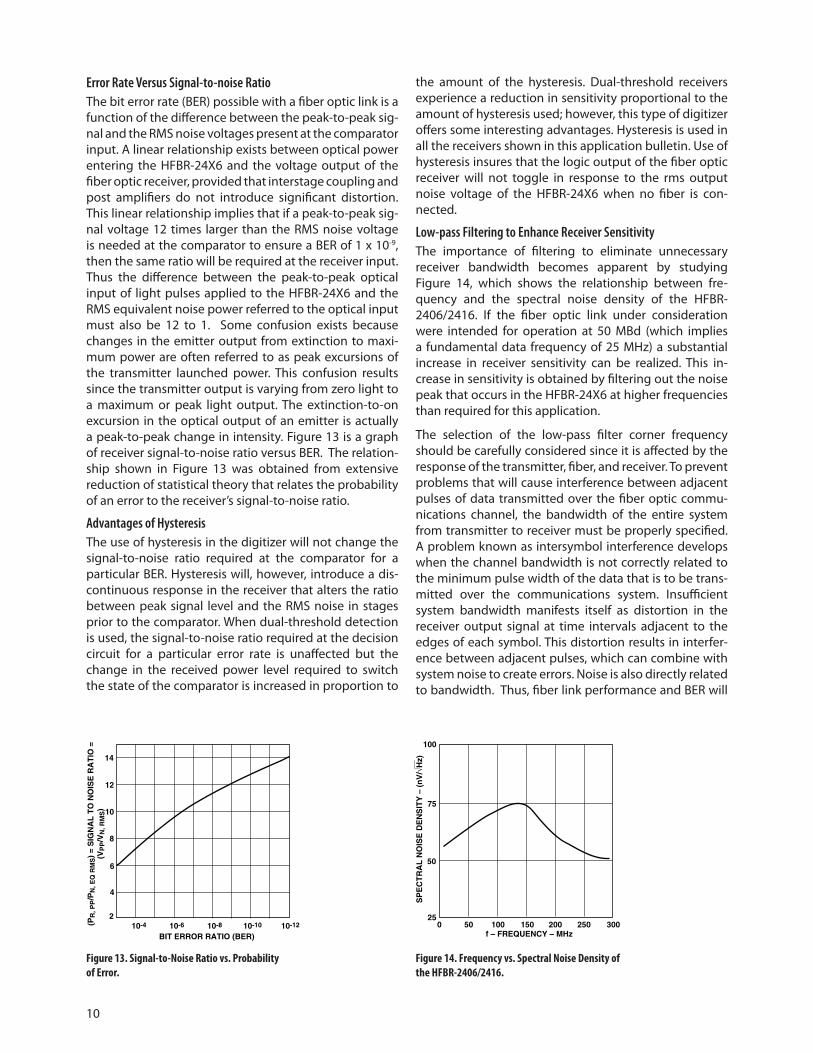
Error Rate Versus Signal-to-noise RatioThe bit error rate (BER) possible with a fiber optic link is a function of the difference between the peak-to-peak sig-nal and the RMS noise voltages present at the comparator input. A linear relationship exists between optical power entering the HFBR-24X6 and the voltage output of the fiber optic receiver, provided that interstage coupling and post amplifiers do not introduce significant distortion. This linear relationship implies that if a peak-to-peak sig-nal voltage 12 times larger than the RMS noise voltage is needed at the comparator to ensure a BER of 1 x 10⁻⁹, then the same ratio will be required at the receiver input. Thus the difference between the peak-to-peak optical input of light pulses applied to the HFBR-24X6 and the RMS equivalent noise power referred to the optical input must also be 12 to 1. Some confusion exists because changes in the emitter output from extinction to maxi-mum power are often referred to as peak excursions of the transmitter launched power. This confusion results since the transmitter output is varying from zero light to a maximum or peak light output. The extinction-to-on excursion in the optical output of an emitter is actually a peak-to-peak change in intensity. Figure 13 is a graph of receiver signal-to-noise ratio versus BER. The relation-ship shown in Figure 13 was obtained from extensive reduction of statistical theory that relates the probability of an error to the receiver’s signal-to-noise ratio.
Advantages of HysteresisThe use of hysteresis in the digitizer will not change the signal-to-noise ratio required at the comparator for a particular BER. Hysteresis will, however, introduce a dis-continuous response in the receiver that alters the ratio between peak signal level and the RMS noise in stages prior to the comparator. When dual-threshold detection is used, the signal-to-noise ratio required at the decision circuit for a particular error rate is unaffected but the change in the received power level required to switch the state of the comparator is increased in proportion to
the amount of the hysteresis. Dual-threshold receivers experience a reduction in sensitivity proportional to the amount of hysteresis used; however, this type of digitizer offers some interesting advantages. Hysteresis is used in all the receivers shown in this application bulletin. Use of hysteresis insures that the logic output of the fiber optic receiver will not toggle in response to the rms output noise voltage of the HFBR-24X6 when no fiber is con-nected.
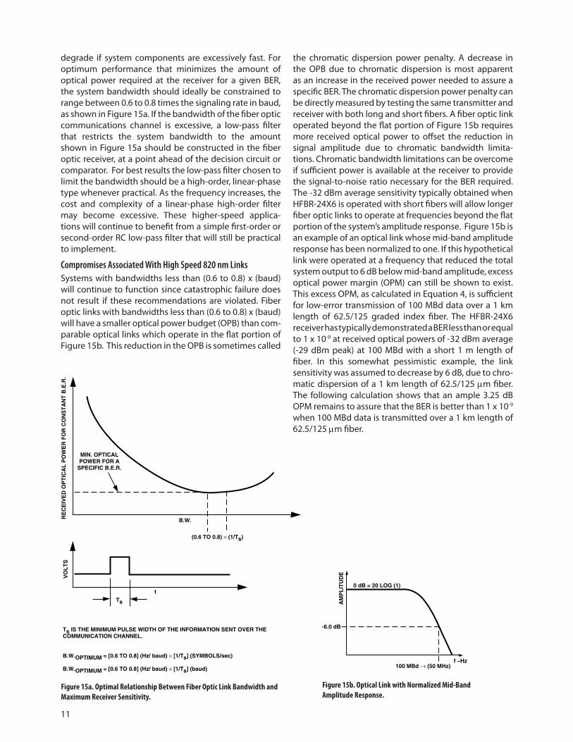
Low-pass Filtering to Enhance Receiver SensitivityThe importance of filtering to eliminate unnecessary receiver bandwidth becomes apparent by studying Figure 14, which shows the relationship between fre-quency and the spectral noise density of the HFBR-2406/2416. If the fiber optic link under consideration were intended for operation at 50 MBd (which implies a fundamental data frequency of 25 MHz) a substantial increase in receiver sensitivity can be realized. This in-crease in sensitivity is obtained by filtering out the noise peak that occurs in the HFBR-24X6 at higher frequencies than required for this application.
The selection of the low-pass filter corner frequency should be carefully considered since it is affected by the response of the transmitter, fiber, and receiver. To prevent problems that will cause interference between adjacent pulses of data transmitted over the fiber optic commu-nications channel, the bandwidth of the entire system from transmitter to receiver must be properly specified. A problem known as intersymbol interference develops when the channel bandwidth is not correctly related to the minimum pulse width of the data that is to be trans-mitted over the communications system. Insufficient system bandwidth manifests itself as distortion in the receiver output signal at time intervals adjacent to the edges of each symbol. This distortion results in interfer-ence between adjacent pulses, which can combine with system noise to create errors. Noise is also directly related to bandwidth. Thus, fiber link performance and BER will
100
75
50
25
SP
EC
TR
AL
NO
ISE
DE
NS
ITY
– (
nV
/√H
z)
0 50 100 150 200 250 300f – FREQUENCY – MHz
5357-14
100
75
50
25
SP
EC
TR
AL
NO
ISE
DE
NS
ITY
– (
nV
/√H
z)
0 50 100 150 200 250 300f – FREQUENCY – MHz
7
6
5
4
3
2
1(P
PR
CV
R/P
EQ
INrm
s) =
SIG
NA
L T
O N
OIS
E R
AT
IO =
(VP/V
rms
NO
ISE
)10-4 10-6 10-8 10-10 10-12
BIT ERROR RATIO (BER)
5357-13
14
12
10
8
6
4
2
(PR
, PP/P
N, E
Q R
MS)
= S
IGN
AL
TO
NO
ISE
RA
TIO
=(V
PP/V
N, R
MS)
10-4 10-6 10-8 10-10 10-12
BIT ERROR RATIO (BER)
14
12
10
8
6
4
2
(PR
, PP/P
N, E
Q R
MS
) =
SIG
NA
L T
O N
OIS
E R
AT
IO =
(VP
P/V
N, R
MS
)
10-4 10-6 10-8 10-10 10-12
BIT ERROR RATIO (BER)
11
Figure 15a. Optimal Relationship Between Fiber Optic Link Bandwidth and Maximum Receiver Sensitivity.
Figure 15b. Optical Link with normalized Mid-Band Amplitude Response.
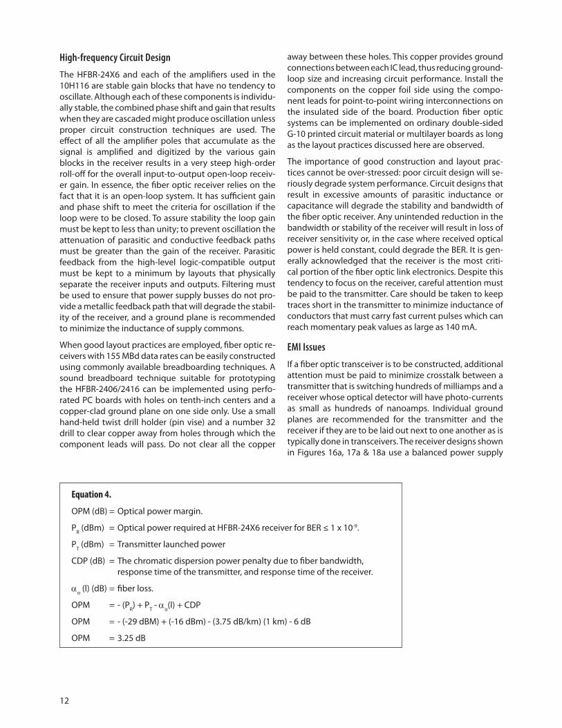
degrade if system components are excessively fast. For optimum performance that minimizes the amount of optical power required at the receiver for a given BER, the system bandwidth should ideally be constrained to range between 0.6 to 0.8 times the signaling rate in baud, as shown in Figure 15a. If the bandwidth of the fiber optic communications channel is excessive, a low-pass filter that restricts the system bandwidth to the amount shown in Figure 15a should be constructed in the fiber optic receiver, at a point ahead of the decision circuit or comparator. For best results the low-pass filter chosen to limit the bandwidth should be a high-order, linear-phase type whenever practical. As the frequency increases, the cost and complexity of a linear-phase high-order filter may become excessive. These higher-speed applica-tions will continue to benefit from a simple first-order or second-order RC low-pass filter that will still be practical to implement.
Compromises Associated With High Speed 820 nm LinksSystems with bandwidths less than (0.6 to 0.8) x (baud) will continue to function since catastrophic failure does not result if these recommendations are violated. Fiber optic links with bandwidths less than (0.6 to 0.8) x (baud) will have a smaller optical power budget (OPB) than com-parable optical links which operate in the flat portion of Figure 15b. This reduction in the OPB is sometimes called
the chromatic dispersion power penalty. A decrease in the OPB due to chromatic dispersion is most apparent as an increase in the received power needed to assure a specific BER. The chromatic dispersion power penalty can be directly measured by testing the same transmitter and receiver with both long and short fibers. A fiber optic link operated beyond the flat portion of Figure 15b requires more received optical power to offset the reduction in signal amplitude due to chromatic bandwidth limita-tions. Chromatic bandwidth limitations can be overcome if sufficient power is available at the receiver to provide the signal-to-noise ratio necessary for the BER required. The -32 dBm average sensitivity typically obtained when HFBR-24X6 is operated with short fibers will allow longer fiber optic links to operate at frequencies beyond the flat portion of the system’s amplitude response. Figure 15b is an example of an optical link whose mid-band amplitude response has been normalized to one. If this hypothetical link were operated at a frequency that reduced the total system output to 6 dB below mid-band amplitude, excess optical power margin (OPM) can still be shown to exist. This excess OPM, as calculated in Equation 4, is sufficient for low-error transmission of 100 MBd data over a 1 km length of 62.5/125 graded index fiber. The HFBR-24X6 receiver has typically demonstrated a BER less than or equal to 1 x 10⁻⁹ at received optical powers of -32 dBm average (-29 dBm peak) at 100 MBd with a short 1 m length of fiber. In this somewhat pessimistic example, the link sensitivity was assumed to decrease by 6 dB, due to chro-matic dispersion of a 1 km length of 62.5/125 µm fiber. The following calculation shows that an ample 3.25 dB OPM remains to assure that the BER is better than 1 x 10⁻⁹ when 100 MBd data is transmitted over a 1 km length of 62.5/125 µm fiber.
-6.0 dB
AM
PL
ITU
DE
0 dB = 20 LOG (1)
f –Hz100 MBd → (50 MHz)
5357−15β
5357-15a
MIN. OPTICALPOWER FOR A
SPECIFIC B.E.R.
RE
CE
IVE
D O
PT
ICA
L P
OW
ER
FO
R C
ON
ST
AN
T B
.E.R
.
B.W.
(0.6 TO 0.8) × (1/Ts)
VO
LT
S
Ts
t
Ts IS THE MINIMUM PULSE WIDTH OF THE INFORMATION SENT OVER THE COMMUNICATION CHANNEL.
B.W.OPTIMUM = [0.6 TO 0.8] (Hz/ baud) × [1/Ts] (SYMBOLS/sec)
B.W.OPTIMUM = [0.6 TO 0.8] (Hz/ baud) × [1/Ts] (baud)
12
High-frequency Circuit Design
The HFBR-24X6 and each of the amplifiers used in the 10H116 are stable gain blocks that have no tendency to oscillate. Although each of these components is individu-ally stable, the combined phase shift and gain that results when they are cascaded might produce oscillation unless proper circuit construction techniques are used. The effect of all the amplifier poles that accumulate as the signal is amplified and digitized by the various gain blocks in the receiver results in a very steep high-order roll-off for the overall input-to-output open-loop receiv-er gain. In essence, the fiber optic receiver relies on the fact that it is an open-loop system. It has sufficient gain and phase shift to meet the criteria for oscillation if the loop were to be closed. To assure stability the loop gain must be kept to less than unity; to prevent oscillation the attenuation of parasitic and conductive feedback paths must be greater than the gain of the receiver. Parasitic feedback from the high-level logic-compatible output must be kept to a minimum by layouts that physically separate the receiver inputs and outputs. Filtering must be used to ensure that power supply busses do not pro-vide a metallic feedback path that will degrade the stabil-ity of the receiver, and a ground plane is recommended to minimize the inductance of supply commons.
When good layout practices are employed, fiber optic re-ceivers with 155 MBd data rates can be easily constructed using commonly available breadboarding techniques. A sound breadboard technique suitable for prototyping the HFBR-2406/2416 can be implemented using perfo-rated PC boards with holes on tenth-inch centers and a copper-clad ground plane on one side only. Use a small hand-held twist drill holder (pin vise) and a number 32 drill to clear copper away from holes through which the component leads will pass. Do not clear all the copper
away between these holes. This copper provides ground connections between each IC lead, thus reducing ground-loop size and increasing circuit performance. Install the components on the copper foil side using the compo-nent leads for point-to-point wiring interconnections on the insulated side of the board. Production fiber optic systems can be implemented on ordinary double-sided G-10 printed circuit material or multilayer boards as long as the layout practices discussed here are observed.
The importance of good construction and layout prac-tices cannot be over-stressed: poor circuit design will se-riously degrade system performance. Circuit designs that result in excessive amounts of parasitic inductance or capacitance will degrade the stability and bandwidth of the fiber optic receiver. Any unintended reduction in the bandwidth or stability of the receiver will result in loss of receiver sensitivity or, in the case where received optical power is held constant, could degrade the BER. It is gen-erally acknowledged that the receiver is the most criti-cal portion of the fiber optic link electronics. Despite this tendency to focus on the receiver, careful attention must be paid to the transmitter. Care should be taken to keep traces short in the transmitter to minimize inductance of conductors that must carry fast current pulses which can reach momentary peak values as large as 140 mA.
EMI Issues
If a fiber optic transceiver is to be constructed, additional attention must be paid to minimize crosstalk between a transmitter that is switching hundreds of milliamps and a receiver whose optical detector will have photo-currents as small as hundreds of nanoamps. Individual ground planes are recommended for the transmitter and the receiver if they are to be laid out next to one another as is typically done in transceivers. The receiver designs shown in Figures 16a, 17a & 18a use a balanced power supply
Equation 4.
OPM (dB) = Optical power margin.
PR (dBm) = Optical power required at HFBR-24X6 receiver for BER ≤ 1 x 10⁻⁹.
PT (dBm) = Transmitter launched power
CDP (dB) = The chromatic dispersion power penalty due to fiber bandwidth, response time of the transmitter, and response time of the receiver.
αo (l) (dB) = fiber loss.
OPM = - (PR) + P
T - α
o(l) + CDP
OPM = - (-29 dBM) + (-16 dBm) - (3.75 dB/km) (1 km) - 6 dB
OPM = 3.25 dB
13
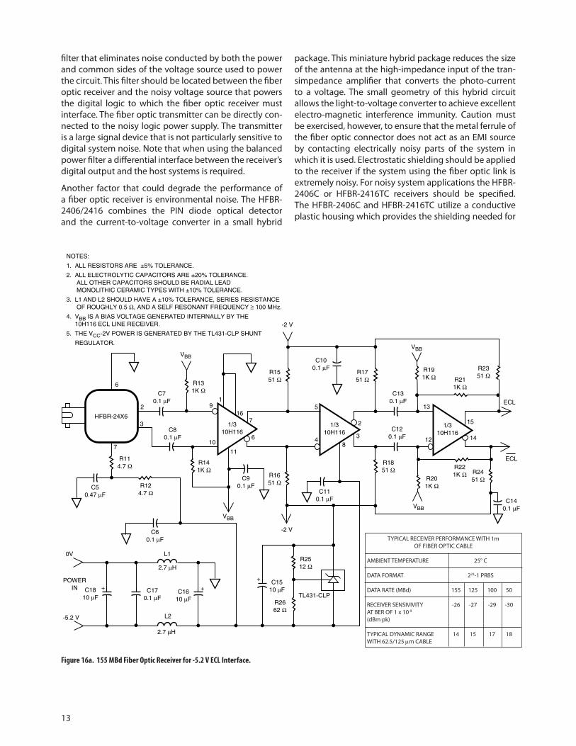
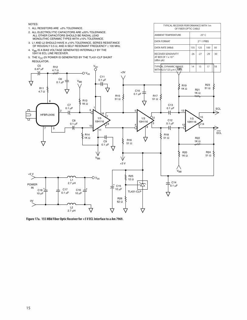
filter that eliminates noise conducted by both the power and common sides of the voltage source used to power the circuit. This filter should be located between the fiber optic receiver and the noisy voltage source that powers the digital logic to which the fiber optic receiver must interface. The fiber optic transmitter can be directly con-nected to the noisy logic power supply. The transmitter is a large signal device that is not particularly sensitive to digital system noise. Note that when using the balanced power filter a differential interface between the receiver’s digital output and the host systems is required.
Another factor that could degrade the performance of a fiber optic receiver is environmental noise. The HFBR-2406/2416 combines the PIN diode optical detector and the current-to-voltage converter in a small hybrid
package. This miniature hybrid package reduces the size of the antenna at the high-impedance input of the tran-simpedance amplifier that converts the photo-current to a voltage. The small geometry of this hybrid circuit allows the light-to-voltage converter to achieve excellent electro-magnetic interference immunity. Caution must be exercised, however, to ensure that the metal ferrule of the fiber optic connector does not act as an EMI source by contacting electrically noisy parts of the system in which it is used. Electrostatic shielding should be applied to the receiver if the system using the fiber optic link is extremely noisy. For noisy system applications the HFBR-2406C or HFBR-2416TC receivers should be specified. The HFBR-2406C and HFBR-2416TC utilize a conductive plastic housing which provides the shielding needed for
Figure 16a. 155 MBd Fiber Optic Receiver for -5.2 V ECL Interface.
TYPICAL RECEIVER PERFORMANCE WITH 1m OF FIBER OPTIC CABLE
AMBIENT TEMPERATURE 25° C
DATA FORMAT 223-1 PRBS
DATA RATE (MBd) 155 125 100 50
RECEIVER SENSIVIVITY -26 -27 -29 -30AT BER OF 1 x 10⁻⁹
(dBm pk)
TYPICAL DYNAMIC RANGE 14 15 17 18WITH 62.5/125 µm CABLE
1/310H116
1/310H116
1/310H116
6
2
3
7
C70.1 µF
R131K Ω
19
10
11
6
7
C80.1 µF
16
R141K Ω
R114.7 Ω
R124.7 Ω
C50.47 µF
C60.1 µF
2.7 µH
C1810 µF
C170.1 µF
C1610 µF
2.7 µH
-5.2 V
0V
VBB
VBB
C90.1 µF
C1510 µF
R2512 Ω
R2662 Ω
TL431-CLP
C140.1 µF
R201K Ω
-2 V
R1651 Ω
C110.1 µF
5
48
3
2
C100.1 µF
R1751 Ω
R1551 Ω
VBB
-2 V
R191K Ω R21
1K Ω
R2351 Ω
C130.1 µF
C120.1 µF
R1851 Ω R22
1K Ω R2451 Ω
VBB
HFBR-24X6
13
12 14
15
ECL
ECL
++
5357-16a
POWERIN
L1
L2
+
NOTES:
1. ALL RESISTORS ARE ±5% TOLERANCE.
2. ALL ELECTROLYTIC CAPACITORS ARE ±20% TOLERANCE.ALL OTHER CAPACITORS SHOULD BE RADIAL LEADMONOLITHIC CERAMIC TYPES WITH ±10% TOLERANCE.
3. L1 AND L2 SHOULD HAVE A ±10% TOLERANCE, SERIES RESISTANCEOF ROUGHLY 0.5 Ω, AND A SELF RESONANT FREQUENCY ≥ 100 MHz.
4. VBB IS A BIAS VOLTAGE GENERATED INTERNALLY BY THE 10H116 ECL LINE RECEIVER.
5. THE VCC-2V POWER IS GENERATED BY THE TL431-CLP SHUNT
REGULATOR.
14
Figure 16b. 155 MBd Fiber Optic Transmitter for -5.2 V ECL Interface.
electrically noisy environments. The conductive plastic receivers can be used in systems that have EMI fields as large as 10 volts/meter (see AN-1057). Another method that improves the EMI immunity of the receiver is to use a connector with a non-conductive plastic or ceramic ferrule. In extremely noisy applications the fiber optic re-ceiver can be enclosed in a metal box. This box eliminates noise that would otherwise be coupled into the fiber optic receiver from the system in which it is installed. Systems that require metal shielding have proved to be unusual. Thus, in the majority of applications, the inherent noise immunity of the components combined with the shielding provided by the receiver ground plane have provided sufficient noise immunity.
TYPICAL PEAK POWER COUPLED INTO A 1m LENGTH OF FIBER OPTIC CABLEIF = 60 mA T
A = 25° C
FIBER CABLE NA HFBR-14X2 HFBR-14X4
100/140 µm 0.3 -12.0 -6.5
62.5/125 µm 0.275 -16.0 -12.0
50/125 µm 0.20 -18.8 -15.8
R182 Ω
R282 Ω
R522 Ω
R3120 Ω
R4120 Ω
R691 Ω
R791 Ω
ECL (+)
ECL (–)MPS536
Q1MPS536
Q2
C10.1 µF
74ACTQ001
23 74ACTQ00
74ACTQ00
U1
U1
U1
9
10
13
12
54
6
11
814
7
C475 pF
2, 6, 7
3
5357-16b
U1
R833 Ω
R933 Ω
R10270 Ω
-5 V VEEC2
0.1 µF
C310 µF+
HFBR-14X2/4
NOTES:
1. ALL RESISTORS ARE ±5% TOLERANCE.
2. ALL ELECTROLYTIC CAPACITORS ARE ±20% TOLERANCE.ALL OTHER CAPACITORS SHOULD BE RADIAL LEADMONOLITHIC CERAMIC TYPES WITH ±10% TOLERANCE.
15
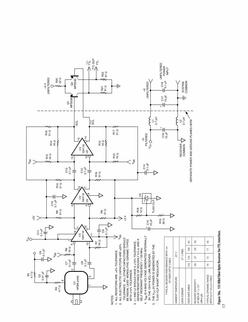
Figure 17a. 155 MBd Fiber Optic Receiver for +5 V ECL Interface to a Am 7969.
TYPICAL RECEIVER PERFORMANCE WITH 1m OF FIBER OPTIC CABLE
AMBIENT TEMPERATURE 25° C
DATA FORMAT 223-1 PRBS
DATA RATE (MBd) 155 125 100 50
RECEIVER SENSIVIVITY -26 -27 -29 -30AT BER OF 1 x 10⁻⁹
(dBm pk)
TYPICAL DYNAMIC RANGE 14 15 17 18WITH 62.5/125 µm CABLE
C110.1 µF
1/310H116
1/310H116
1/310H116
6
2
37
C70.1 µF
R131K Ω
19
10
11
6
7
C80.1 µF
16
R141K Ω
L12.7 µH
C1810 µF
C170.1 µF
C1610 µF
L22.7 µH
+5 V
0V
VBB
VBB
C90.1 µF
C1510 µF
R2512 Ω
R2662 Ω
TL431-CLP
C140.1 µF
R201K Ω
+3 V
R1651 Ω
5
48
3
2
C100.1 µF
R1751 Ω
R1551 Ω
VBB
+3V
R191K Ω R21
1K Ω
R2351 Ω
C130.1 µF
C120.1 µF
R1851 Ω R22
1K Ω
R2451 Ω
VBB
HFBR-24X6
13
12 14
15
ECL
ECL
++
5357-17a
C50.47 µF
C60.1 µF
R114.7 Ω
R124.7 Ω
Vcc
Vcc
Vcc
POWERIN
+
NOTES:
1. ALL RESISTORS ARE ±5% TOLERANCE.
2. ALL ELECTROLYTIC CAPACITORS ARE ±20% TOLERANCE.ALL OTHER CAPACITORS SHOULD BE RADIAL LEADMONOLITHIC CERAMIC TYPES WITH ±10% TOLERANCE.
3. L1 AND L2 SHOULD HAVE A ±10% TOLERANCE, SERIES RESISTANCEOF ROUGHLY 0.5 Ω, AND A SELF RESONANT FREQUENCY ≥ 100 MHz.
4. VBB IS A BIAS VOLTAGE GENERATED INTERNALLY BY THE 10H116 ECL LINE RECEIVER.
5. THE VCC-2V POWER IS GENERATED BY THE TL431-CLP SHUNT
REGULATOR.
16
Figure 17b. 155 MBd Transmitter for +5 V ECL Interface to a Am 7968.
TYPICAL PEAK POWER COUPLED INTO A 1m LENGTH OF FIBER OPTIC CABLEIF = 60 mA T
A = 25° C
FIBER CABLE NA HFBR-14X2 HFBR-14X4
100/140 µm 0.3 -12.0 -6.5
62.5/125 µm 0.275 -16.0 -12.0
50/125 µm 0.20 -18.8 -15.8
Applications Support
Some complete designs that allow the use of HFBR-2406/2416 for run-length-limited data applications will now be discussed. Various transceivers have been designed which permit the HFBR-2406/2416 to be interfaced with:
1. ECL logic operating on -5.2 V. (Figure 16)
2. The AMD TAXIchipTM +5 V 100K ECL interface. (Figure 17)
3. TTL logic operated on +5 V. (Figure 18)
At an ambient temperature of 25° C all three interface circuits provided a typical receiver sensitivity of -29 dBm average with a BER of 1 x 10⁻⁹ at a data rate of 155 MBd.
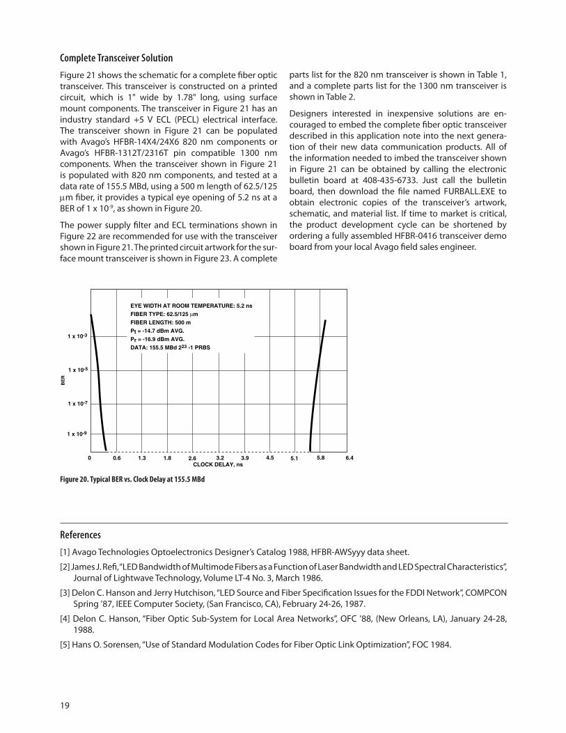
Sensitivity at 125 MBd is typically -30 dBm average at a BER of 1 x 10⁻⁹. Figure 19 shows the typical performance of the ECL transmitter/receiver at 25° C. Note that in this test a 223-1 PRBS pattern at 155 MBd was transmitted over 500 m of 62.5/125 µm graded-index fiber at a BER less than 1 x 10⁻⁹. If the low-cost, high-performance fiber optic links possible with the HFBR-2406/2416 interest you, contact your local Avago field sales engineer for ad-ditional assistance. Your local Avago sales representative can simplify your prototyping task by providing complete artwork for the fiber optic transmitters and receivers discussed in this application bulletin.
*TAXIchip is a registered trademark of Advanced Micro Devices Inc.
R182 Ω
R282 Ω
R522 Ω
R3120 Ω
R4120 Ω
R691 Ω
R791 Ω
+5 V Vcc
ECL (+)
ECL (–)MPS536
Q1MPS536
Q2
C10.1 µF
74ACTQ001
23 74ACTQ00
74ACTQ00
U1
U1
U1
9
10
13
12
54
6
11
814
7
C475 pF
C20.1 µF
C310 µF
2, 6, 7
3
5357-17b
U1
+
R833 Ω
R933 Ω
R10270 Ω
HFBR-14X2/4
NOTES:
1. ALL RESISTORS ARE ±5% TOLERANCE.
2. ALL ELECTROLYTIC CAPACITORS ARE ±20% TOLERANCE.ALL OTHER CAPACITORS SHOULD BE RADIAL LEADMONOLITHIC CERAMIC TYPES WITH ±10% TOLERANCE.
TYPI
CA
L RE
CEI
VER
PERF
ORM
AN
CE
WIT
H 1
m
OF
FIBE
R O
PTIC
CA
BLE
AM
BIEN
T TE
MPE
RATU
RE
25° C
DAT
A F
ORM
AT
223-1
PRB
S
DAT
A R
ATE
(MBd
) 15
5 12
5 10
0 50
REC
EIVE
R SE
NSI
VIVI
TY
-26
-27
-29
-30
AT B
ER O
F 1
x 10
-9
(dBm
pk)
TYPI
CA
L D
YNA
MIC
RA
NG
E 14
15
17
18
WIT
H 6
2.5/
125 µm
CA
BLE
Figu
re 1
8a. 1
55 M
Bd Fi
ber O
ptic
Rece
iver
for T
TL In
terf
ace.
17
1/3
10H
116
1/3
10H
116
1/3
10H
116
6
2
37
C7
0.1 µF
R6
1K Ω
19 10
11
67
C8
0.1 µF
16
R7
1K Ω
L12.
7 µH
C16
10 µ
F
C17
10 µ
FC
180.
1 µF
L22.
7 µH
RE
CE
IVE
RC
OM
MO
N
VB
B
VB
B
C9
0.1 µF
C15
10 µ
F
R18
12 Ω
R19
62 Ω
TL4
31-C
LP
C14
0.1 µF
R13
1K Ω
+3
V
R9
51 Ω
5 48
32
C10
0.1 µF
R10
51 Ω
R8
51 Ω
VB
B
+3V
R12
1K Ω
R14
1K Ω
R16
51 Ω
C13
0.1 µF
C12
0.1 µF
R18
51 Ω
R15
1K Ω
R17
51 Ω
VB
B
U1
HF
BR
-24X
6
13 121415
EC
L
EC
L
+
5357-18a
R4
4.7 Ω
R5
4.7 Ω
Vcc
C11
0.1 µF
Vcc
+
C6
0.1 µF
C5
0.47
µF
R20
22 Ω
R21
91 Ω
R22
91 Ω
Q1
MP
S53
6Q
2M
PS
536
+5
VU
NF
ILT
ER
ED
TT
L
TT
L
TT
L O
UT
+5
FIL
TE
RE
D
+
+5
UN
FIL
TE
RE
D
UN
FIL
TE
RE
DP
OW
ER
INP
UT
SY
ST
EM
CO
MM
ON
SE
PA
RA
TE
PO
WE
R A
ND
GR
OU
ND
PLA
NE
S H
ER
E
U2
U2
U3
NO
TE
S:
1. A
LL R
ES
IST
OR
S A
RE
±5%
TO
LER
AN
CE
.
2. A
LL E
LEC
TR
OLY
TIC
CA
PA
CIT
OR
S A
RE
±20
%
TO
LER
AN
CE
. A
LL O
TH
ER
CA
PA
CIT
OR
S S
HO
ULD
BE
RA
DIA
L LE
AD
MO
NO
LIT
HIC
CE
RA
MIC
TY
PE
S
W
ITH
±10
% T
OLE
RA
NC
E.
3. L
1 A
ND
L2
SH
OU
LD H
AV
E A
±10
% T
OLE
RA
NC
E,
S
ER
IES
RE
SIS
TA
NC
E O
F R
OU
GH
LY 0
.5 Ω
, AN
D A
SE
LF R
ES
ON
AN
T F
RE
QU
EN
CY
≥ 1
00 M
Hz.
4. V
BB
IS A
BIA
S V
OLT
AG
E G
EN
ER
AT
ED
INT
ER
NA
LLY
BY
TH
E 1
0H11
6 E
CL
LIN
E R
EC
EIV
ER
.
5. T
HE
VC
C-2
V P
OW
ER
IS G
EN
ER
AT
ED
BY
TH
E
T
L431
-CLP
SH
UN
T R
EG
ULA
TO
R.
18
5357-19
FIBER LENGTH 500 m
TYPICAL PEAK-TO-PEAK JITTER = 760 ps
TIME SCALE IS 2.0 ns/DIV.
DATA RATE 155 MBd
DATA PATTERN 223-1 PRBS
FIBER TYPE SIECOR 62.5/125 µm
Figure 18b. 155 MBd Fiber Optic Transmitter for TTL Interface.
Figure 19. ECL Output of the Transceiver Shown in Figures 17a and 17b.
TYPICAL PEAK POWER COUPLED INTO A 1m LENGTH OF FIBER OPTIC CABLEIF = 60 mA T
A = 25° C
FIBER CABLE NA HFBR-14X2 HFBR-14X4
100/140 µm 0.3 -12.0 -6.5
62.5/125 µm 0.275 -16.0 -12.0
50/125 µm 0.20 -18.8 -15.8
+5 V Vcc
74ACTQ001
23 74ACTQ00
74ACTQ00
U1
U1
U1
9
10
13
12
54
6
11
814
7
C175 pF
R133 Ω
C20.1 µF
C310 µF
2, 6, 7
3
5357-18b
U1
+
TTLIN
R233 Ω
R3270 Ω
HFBR-14X2/4
NOTES:
1. ALL RESISTORS ARE ±5% TOLERANCE.
2. ALL ELECTROLYTIC CAPACITORS ARE ±20% TOLERANCE.ALL OTHER CAPACITORS SHOULD BE RADIAL LEADMONOLITHIC CERAMIC TYPES WITH ±10% TOLERANCE.
19
Complete Transceiver Solution
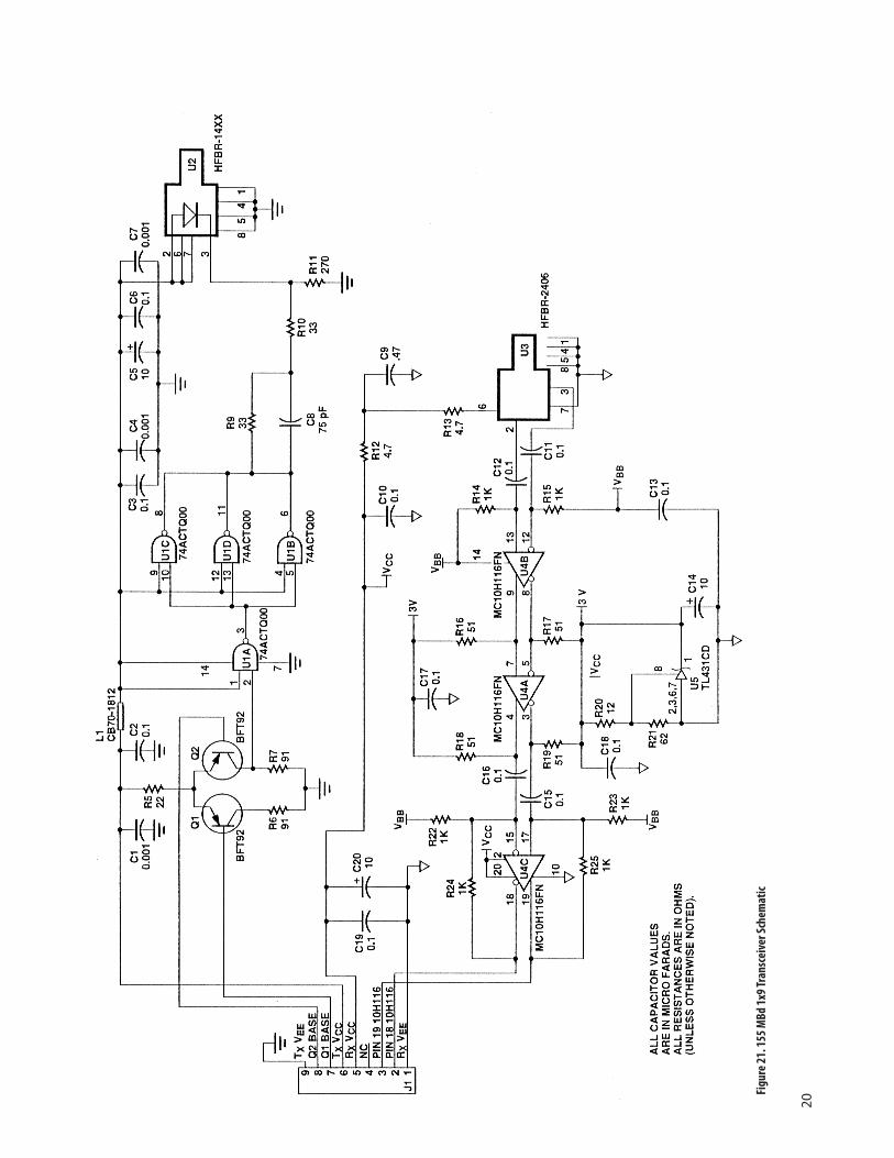
Figure 21 shows the schematic for a complete fiber optic transceiver. This transceiver is constructed on a printed circuit, which is 1" wide by 1.78" long, using surface mount components. The transceiver in Figure 21 has an industry standard +5 V ECL (PECL) electrical interface. The transceiver shown in Figure 21 can be populated with Avago’s HFBR-14X4/24X6 820 nm components or Avago’s HFBR-1312T/2316T pin compatible 1300 nm components. When the transceiver shown in Figure 21 is populated with 820 nm components, and tested at a data rate of 155.5 MBd, using a 500 m length of 62.5/125 µm fiber, it provides a typical eye opening of 5.2 ns at a BER of 1 x 10⁻⁹, as shown in Figure 20.
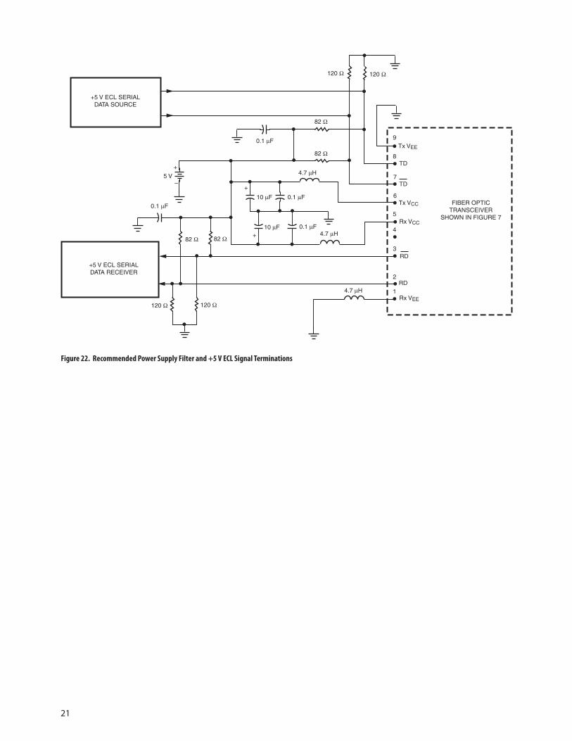
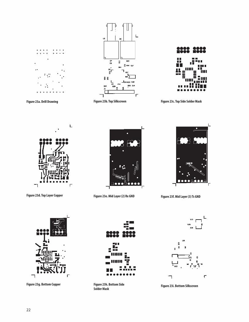
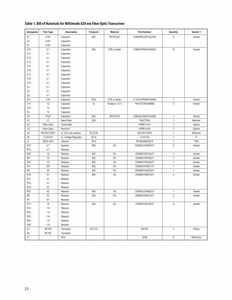
The power supply filter and ECL terminations shown in Figure 22 are recommended for use with the transceiver shown in Figure 21. The printed circuit artwork for the sur-face mount transceiver is shown in Figure 23. A complete
parts list for the 820 nm transceiver is shown in Table 1, and a complete parts list for the 1300 nm transceiver is shown in Table 2.
Designers interested in inexpensive solutions are en-couraged to embed the complete fiber optic transceiver described in this application note into the next genera-tion of their new data communication products. All of the information needed to imbed the transceiver shown in Figure 21 can be obtained by calling the electronic bulletin board at 408-435-6733. Just call the bulletin board, then download the file named FURBALL.EXE to obtain electronic copies of the transceiver’s artwork, schematic, and material list. If time to market is critical, the product development cycle can be shortened by ordering a fully assembled HFBR-0416 transceiver demo board from your local Avago field sales engineer.
1 x 10⁻³
1 x 10⁻⁵
1 x 10⁻⁷
1 x 10⁻⁹
BE
R
0 0.6 1.3 2.61.8 3.2 3.9 4.5 5.1 5.8 6.4CLOCK DELAY, ns
EYE WIDTH AT ROOM TEMPERATURE: 5.2 ns
FIBER TYPE: 62.5/125 µm
FIBER LENGTH: 500 m
Pt = -14.7 dBm AVG.
Pr = -16.9 dBm AVG.
DATA: 155.5 MBd 223 -1 PRBS
5684-21 AB 78
Figure 20. Typical BER vs. Clock Delay at 155.5 MBd
References
[1] Avago Technologies Optoelectronics Designer’s Catalog 1988, HFBR-AWSyyy data sheet.
[2] James J. Refi, “LED Bandwidth of Multimode Fibers as a Function of Laser Bandwidth and LED Spectral Characteristics”, Journal of Lightwave Technology, Volume LT-4 No. 3, March 1986.
[3] Delon C. Hanson and Jerry Hutchison, “LED Source and Fiber Specification Issues for the FDDI Network”, COMPCON Spring ’87, IEEE Computer Society, (San Francisco, CA), February 24-26, 1987.
[4] Delon C. Hanson, “Fiber Optic Sub-System for Local Area Networks”, OFC ’88, (New Orleans, LA), January 24-28, 1988.
[5] Hans O. Sorensen, “Use of Standard Modulation Codes for Fiber Optic Link Optimization”, FOC 1984.
Figu
re 2
1. 1
55 M
Bd 1
x9 Tr
ansc
eive
r Sch
emat
ic
20
21
+5 V ECL SERIALDATA SOURCE
+
+
+
–5 V
82 Ω 82 Ω
120 Ω 120 Ω
0.1 µF
0.1 µF
0.1 µF
0.1 µF4.7 µH
4.7 µH
4.7 µH
10 µF
10 µF
+5 V ECL SERIALDATA RECEIVER
82 Ω
120 Ω 120 Ω
82 Ω
9
8
7
6
5
3
4
2
1
FIBER OPTICTRANSCEIVER
SHOWN IN FIGURE 7
Tx VEE
TD
TD
Tx VCC
Rx VCC
RD
RD
Rx VEE
5684-22 AB 78
Figure 22. Recommended Power Supply Filter and +5 V ECL Signal Terminations
22
Figure 23d. Top Layer Copper Figure 23e. Mid Layer (2) Rx GnD Figure 23f. Mid Layer (3) Ts GnD
Figure 23g. Bottom Copper Figure 23h. Bottom Side Solder Mask
Figure 23i. Bottom Silkscreen
Figure 23a. Drill Drawing Figure 23b. Top Silkscreen Figure 23c. Top Side Solder Mask
23
Table 1. Bill of Materials for Miltimode 820 nm Fiber Optic Transceiver
Deslgnator Part Type Description Footprint Material Part Number Quantity Vendor 1
C1 0.001 Capacitor 805 NPO/COG C0805NPO500102JNE 3 VenkelC4 0.001 CapacitorC7 0.001 CapacitorC10 0.1 Capacitor 805 X7R or better C0805X7R500104KNE 12 VenkelC11 0.1 CapacitorC12 0.1 CapacitorC13 0.1 CapacitorC15 0.1 CapacitorC16 0.1 CapacitorC17 0.1 CapacitorC18 0.1 CapacitorC19 0.1 CapacitorC2 0.1 CapacitorC3 0.1 CapacitorC6 0 1 CapacitorC9 0.47 Capacitor 1812 X7R or better C 1812X7R500474KNE 1 VenkelC14 10 Capacitor B Tantalum, 10 V TA010TCM106MBN 3 VenkelC20 10 CapacitorC5 10 CapacitorC8 75 pF Capacitor 805 NPO/COG C0805COG500750JNE 1 VenkelU1 I.C. Nand Gate S08 74ACTQ00 1 NationalU2 Fiber-Optic Transmitter HFBR-1414 1 AgilentU3 Fiber-Optic Receiver HFBR-2416 1 AgilentU4 MC10H116FN IC, ECL line receiver PLCC20 MC10H116FN 1 MotorolaU5 TL431CD IC, Voltage Regulator SO-8 TL431CD 1 T.l.L1 CB70-1812 Inductor 1812 HF30ACB453215 1 TDKR12 4.7 Resistor 805 5% CR08051OW4R7JT 2 VenkelR13 4.7 ResistorR20 12 Resistor 805 5% CR080510W120JT 1 VenkelR9 33 Resistor 805 5% CR080510W330JT 1 VenkelR10 33 Resistor 805 5% CR080510W330JT 1 VenkelR11 270 Resistor 805 5% CR080510W271JT 1 VenkelR5 22 Resistor 805 5% CR08051OW220JT 1 VenkelR16 51 Resistor 805 5% CR080510W510JT 4 VenkelR17 51 ResistorR18 51 ResistorR19 51 ResistorR21 62 Resistor 805 5% CR08051OW620JT 1 VenkelR6 91 Resistor 805 5% CR080510W91OJT 2 VenkelR7 91 Resistor R14 1K Resistor 805 5% CR080510W102JT 6 VenkelR15 1 K ResistorR22 1 K ResistorR23 1 K ResistorR24 1 K ResistorR25 1 K ResistorQ1 BFT92 Transistor SOT-23 BFT92 2 PhilipsQ2 BFT92 TransistorJ1 Pins 343B 9 McKenzie
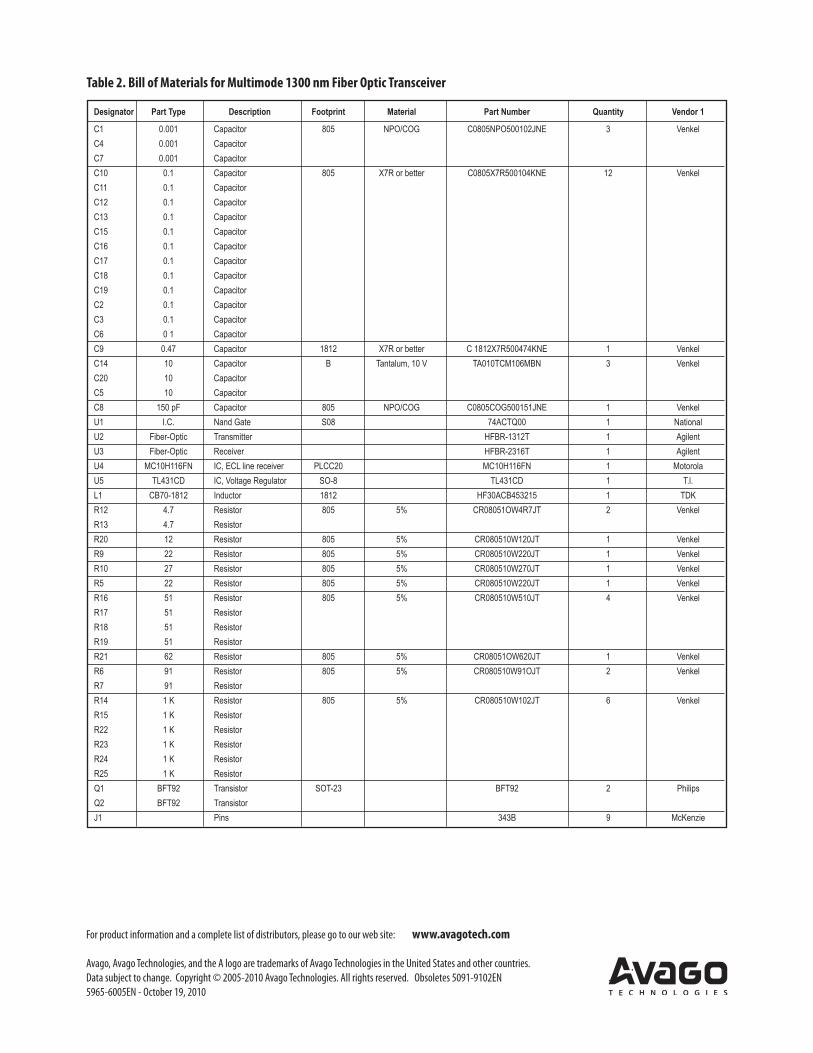
Table 2. Bill of Materials for Multimode 1300 nm Fiber Optic Transceiver
Designator Part Type Description Footprint Material Part Number Quantity Vendor 1
C1 0.001 Capacitor 805 NPO/COG C0805NPO500102JNE 3 VenkelC4 0.001 CapacitorC7 0.001 CapacitorC10 0.1 Capacitor 805 X7R or better C0805X7R500104KNE 12 VenkelC11 0.1 CapacitorC12 0.1 CapacitorC13 0.1 CapacitorC15 0.1 CapacitorC16 0.1 CapacitorC17 0.1 CapacitorC18 0.1 CapacitorC19 0.1 CapacitorC2 0.1 CapacitorC3 0.1 CapacitorC6 0 1 CapacitorC9 0.47 Capacitor 1812 X7R or better C 1812X7R500474KNE 1 VenkelC14 10 Capacitor B Tantalum, 10 V TA010TCM106MBN 3 VenkelC20 10 CapacitorC5 10 CapacitorC8 150 pF Capacitor 805 NPO/COG C0805COG500151JNE 1 VenkelU1 I.C. Nand Gate S08 74ACTQ00 1 NationalU2 Fiber-Optic Transmitter HFBR-1312T 1 AgilentU3 Fiber-Optic Receiver HFBR-2316T 1 AgilentU4 MC10H116FN IC, ECL line receiver PLCC20 MC10H116FN 1 MotorolaU5 TL431CD IC, Voltage Regulator SO-8 TL431CD 1 T.l.L1 CB70-1812 Inductor 1812 HF30ACB453215 1 TDKR12 4.7 Resistor 805 5% CR08051OW4R7JT 2 VenkelR13 4.7 ResistorR20 12 Resistor 805 5% CR080510W120JT 1 VenkelR9 22 Resistor 805 5% CR080510W220JT 1 VenkelR10 27 Resistor 805 5% CR080510W270JT 1 VenkelR5 22 Resistor 805 5% CR080510W220JT 1 VenkelR16 51 Resistor 805 5% CR080510W510JT 4 VenkelR17 51 ResistorR18 51 ResistorR19 51 ResistorR21 62 Resistor 805 5% CR08051OW620JT 1 VenkelR6 91 Resistor 805 5% CR080510W91OJT 2 VenkelR7 91 Resistor R14 1 K Resistor 805 5% CR080510W102JT 6 VenkelR15 1 K ResistorR22 1 K ResistorR23 1 K ResistorR24 1 K ResistorR25 1 K ResistorQ1 BFT92 Transistor SOT-23 BFT92 2 PhilipsQ2 BFT92 TransistorJ1 Pins 343B 9 McKenzie
For product information and a complete list of distributors, please go to our web site: www.avagotech.com
Avago, Avago Technologies, and the A logo are trademarks of Avago Technologies in the United States and other countries.Data subject to change. Copyright © 2005-2010 Avago Technologies. All rights reserved. Obsoletes 5091-9102EN 5965-6005EN - October 19, 2010