Embed Size (px)
Citation preview
energies
Article
Low-Cost I–V Tracer for PV Modules under RealOperating Conditions
Manuel Cáceres 1, Andrés Firman 1 , Jesús Montes-Romero 2,* , Alexis Raúl González Mayans 1,Luis Horacio Vera 1, Eduardo F. Fernández 2 and Juan de la Casa Higueras 2
1 Group of Renewable Energies (GER), Northeastern National University, Corrientes 3400, Argentina;[email protected] (M.C.); [email protected] (A.F.);[email protected] (A.R.G.M.); [email protected] (L.H.V.)
2 IDEA Solar Energy Research Group, Electronics and Automation Engineering Department, University ofJaén, Las Lagunillas Campus, 23071 Jaén, Spain; [email protected] (E.F.F.);[email protected] (J.d.l.C.H.)
* Correspondence: [email protected]; Tel.: +34-953-21-3306
Received: 5 June 2020; Accepted: 14 August 2020; Published: 20 August 2020
Abstract: Solar photovoltaic technologies have undergone significant scientific development. Toensure the transfer of knowledge through the training of qualified personnel, didactic tools that can beacquired or built at a reasonable price are needed. Most training and research centres have restrictionson acquiring specific equipment due to its high cost. With this in mind, this article presents thedevelopment and transfer of a low-cost I–V curve tracer acquisition system. The device is mAde upof embedded systems with all the necessary hardware and software for its operation. The hardwareand software presented are open source and have a low cost, i.e., the estimated mAterial cost of thesystem is less than 200 euros. For its development, four institutions from three different countriesparticipated in the project. Three photovoltaic technologies were used to measure the uncertaintiesrelated to the equipment developed. In addition, the system can be transferred for use as an academicor research tool, as long as the measurement does not need to be certified. Two accredited laboratorieshave certified the low uncertainties in the measurement of the proposed system.
Keywords: current–voltage characteristics; photovoltaic systems; I–V curve tracer; outdoor characterisation
1. Introduction
Renewable energies have experienced significant growth during the last decade. Furthermore,from a technological point of view, the development of more efficient and sustainable systems has beenachieved [1–3]. In this context, electrical energy production through the photovoltaic (PV) conversion ofthe incoming sunlight represents an important alternative due to its inherent characteristics. Comparedto other energy generation systems, the large number of applications and high reliability can behighlighted as some of the most outstanding features of PV [4,5]. Therefore, systematic studies arerequired in order to determine and explain the operation principles of different related technologies [6,7],both existing or in development. This is relevant for mAximising the operational efficiency and toelaborate upon methods used to exploit the electric energy produced [8].
The I–V curve of a PV cell, module or array under determined operating conditions providesinformation related to its electrical behaviour (normal or anomalous) and about its energy generationcapacity [9]. It is the most important and widely used metric to describe the electrical output of a PVdevice [10–12].
PV modules and arrays are built using a series or parallel connection of several cells. In normaloperating conditions, the I–V curve has a similar shape regardless of the cell interconnection. The
Energies 2020, 13, 4320; doi:10.3390/en13174320 www.mdpi.com/journal/energies
Energies 2020, 13, 4320 2 of 17
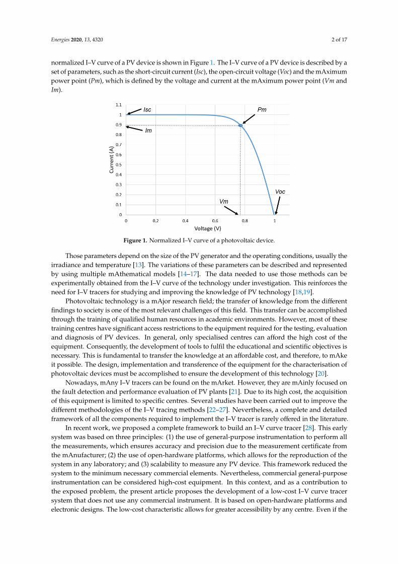
normalized I–V curve of a PV device is shown in Figure 1. The I–V curve of a PV device is described by aset of parameters, such as the short-circuit current (Isc), the open-circuit voltage (Voc) and the mAximumpower point (Pm), which is defined by the voltage and current at the mAximum power point (Vm andIm).
Figure 1. Normalized I–V curve of a photovoltaic device.
Those parameters depend on the size of the PV generator and the operating conditions, usually theirradiance and temperature [13]. The variations of these parameters can be described and representedby using multiple mAthematical models [14–17]. The data needed to use those methods can beexperimentally obtained from the I–V curve of the technology under investigation. This reinforces theneed for I–V tracers for studying and improving the knowledge of PV technology [18,19].
Photovoltaic technology is a mAjor research field; the transfer of knowledge from the differentfindings to society is one of the most relevant challenges of this field. This transfer can be accomplishedthrough the training of qualified human resources in academic environments. However, most of thesetraining centres have significant access restrictions to the equipment required for the testing, evaluationand diagnosis of PV devices. In general, only specialised centres can afford the high cost of theequipment. Consequently, the development of tools to fulfil the educational and scientific objectives isnecessary. This is fundamental to transfer the knowledge at an affordable cost, and therefore, to mAkeit possible. The design, implementation and transference of the equipment for the characterisation ofphotovoltaic devices must be accomplished to ensure the development of this technology [20].
Nowadays, mAny I–V tracers can be found on the mArket. However, they are mAinly focused onthe fault detection and performance evaluation of PV plants [21]. Due to its high cost, the acquisitionof this equipment is limited to specific centres. Several studies have been carried out to improve thedifferent methodologies of the I–V tracing methods [22–27]. Nevertheless, a complete and detailedframework of all the components required to implement the I–V tracer is rarely offered in the literature.
In recent work, we proposed a complete framework to build an I–V curve tracer [28]. This earlysystem was based on three principles: (1) the use of general-purpose instrumentation to perform allthe measurements, which ensures accuracy and precision due to the measurement certificate fromthe mAnufacturer; (2) the use of open-hardware platforms, which allows for the reproduction of thesystem in any laboratory; and (3) scalability to measure any PV device. This framework reduced thesystem to the minimum necessary commercial elements. Nevertheless, commercial general-purposeinstrumentation can be considered high-cost equipment. In this context, and as a contribution tothe exposed problem, the present article proposes the development of a low-cost I–V curve tracersystem that does not use any commercial instrument. It is based on open-hardware platforms andelectronic designs. The low-cost characteristic allows for greater accessibility by any centre. Even if the
Energies 2020, 13, 4320 3 of 17
proposed equipment does not have an individual measurement certificate, extensive validation of themeasurement accuracy has been carried out. The dissemination of this equipment is expected to havea positive impact on the scientific–academic community working in the PV sector. All the necessaryelectronic designs to build the device are included in detail in order to be easily replicated.
The paper is organised as follows: First, the operating principles of all the components of thesystem are provided in detail (Section 2). Second, the methodology used to validate the prototypeis presented (Section 3). Then, the obtained results of this validation are given (Section 4). Finally,the mAin conclusions are presented (Section 5).
2. Operating Principle of the Developed System
In this section, a general description of the mAin components of the system is presented. Thisincludes details in the signal-conditioning circuits. It provides the calibration performed to developand validate the presented prototype. In addition, a simplified budget of the components needed toreplicate the system is provided.
2.1. System Description
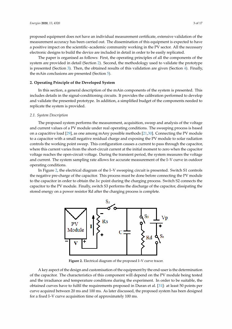
The proposed system performs the measurement, acquisition, sweep and analysis of the voltageand current values of a PV module under real operating conditions. The sweeping process is basedon a capacitive load [29], as one among mAny possible methods [21,30]. Connecting the PV moduleto a capacitor with a small negative residual charge and exposing the PV module to solar radiationcontrols the working point sweep. This configuration causes a current to pass through the capacitor,where this current varies from the short-circuit current at the initial moment to zero when the capacitorvoltage reaches the open-circuit voltage. During the transient period, the system measures the voltageand current. The system sampling rate allows for accurate measurement of the I–V curve in outdooroperating conditions.
In Figure 2, the electrical diagram of the I–V sweeping circuit is presented. Switch S1 controlsthe negative pre-charge of the capacitor. This process must be done before connecting the PV moduleto the capacitor in order to obtain the Isc point during the charging process. Switch S2 connects thecapacitor to the PV module. Finally, switch S3 performs the discharge of the capacitor, dissipating thestored energy on a power resistor Rd after the charging process is complete.
Figure 2. Electrical diagram of the proposed I–V curve tracer.
A key aspect of the design and customisation of the equipment by the end-user is the determinationof the capacitor. The characteristics of this component will depend on the PV module being testedand the irradiance and temperature conditions during the experiment. In order to be suitable, theobtained curves have to fulfil the requirements proposed in Duran et al. [31]: at least 50 points percurve acquired between 20 ms and 100 ms. As later discussed, the proposed system has been designedfor a fixed I–V curve acquisition time of approximately 100 ms.
Energies 2020, 13, 4320 4 of 17
The mAximum capacitor voltage range must be 20% greater than the Voc for safety reasons andmust have low internal resistance. There is no single capacity value that offers a solution to the differenttypes of commercial PV modules and irradiance range outdoors. Therefore, it must be calculated foreach scenario. In Spertino et al. [29], after extensive analysis and experimental work, the capacity C isrecommended to be calculated by using the following expression:
C ' 0.55 tIscVoc
, (1)
where t is the capacitor charging time, which should be higher than 20 ms for Isc and Voc conditionsclose to standard test conditions (STC). In this way, the irradiances range that can be obtained froma particular PV module with the same capacity value is mAximized. For quick modifications of thehardware system, the end-user should evaluate the possibility of connecting the capacitor to theprototype using external connectors.
A shunt resistor (0.5 class 15 A/150 mV) is used for the current measurements [32]. The systemmeasures the voltage on the PV device terminals with a four-wire configuration in order to remove thevoltage drop produced across wires and connectors.
The irradiance and cell temperature are the basic parameters used to define the operatingconditions. In addition, the developed system includes the use of a reference cell [33]. It is composedof two polycrystalline silicon photovoltaic cells. One cell is an irradiance transducer operating at theIsc point with a shunt resistor and the other is used to measure the cell temperature operating at theVoc point. A resistance temperature detector (RTD) PT100 can also acquire the temperature [34].
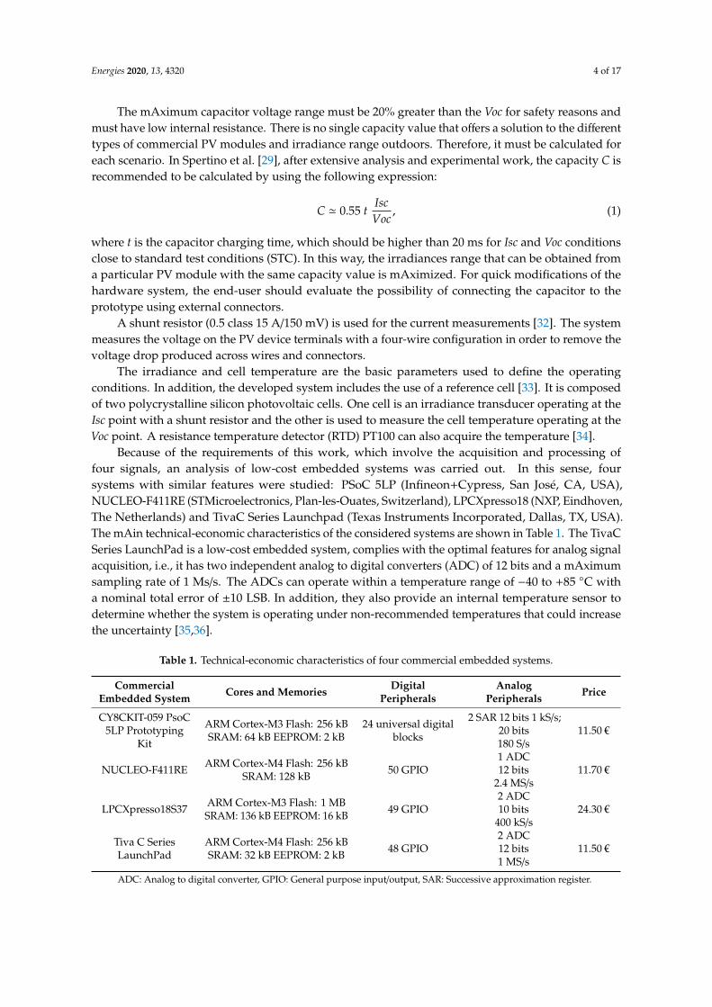
Because of the requirements of this work, which involve the acquisition and processing offour signals, an analysis of low-cost embedded systems was carried out. In this sense, foursystems with similar features were studied: PSoC 5LP (Infineon+Cypress, San José, CA, USA),NUCLEO-F411RE (STMicroelectronics, Plan-les-Ouates, Switzerland), LPCXpresso18 (NXP, Eindhoven,The Netherlands) and TivaC Series Launchpad (Texas Instruments Incorporated, Dallas, TX, USA).The mAin technical-economic characteristics of the considered systems are shown in Table 1. The TivaCSeries LaunchPad is a low-cost embedded system, complies with the optimal features for analog signalacquisition, i.e., it has two independent analog to digital converters (ADC) of 12 bits and a mAximumsampling rate of 1 Ms/s. The ADCs can operate within a temperature range of −40 to +85 C witha nominal total error of ±10 LSB. In addition, they also provide an internal temperature sensor todetermine whether the system is operating under non-recommended temperatures that could increasethe uncertainty [35,36].
Table 1. Technical-economic characteristics of four commercial embedded systems.
CommercialEmbedded System Cores and Memories Digital
PeripheralsAnalog
Peripherals Price
CY8CKIT-059 PsoC5LP Prototyping
Kit
ARM Cortex-M3 Flash: 256 kBSRAM: 64 kB EEPROM: 2 kB
24 universal digitalblocks
2 SAR 12 bits 1 kS/s;20 bits180 S/s
11.50 €
NUCLEO-F411RE ARM Cortex-M4 Flash: 256 kBSRAM: 128 kB 50 GPIO
1 ADC12 bits
2.4 MS/s11.70 €
LPCXpresso18S37 ARM Cortex-M3 Flash: 1 MBSRAM: 136 kB EEPROM: 16 kB 49 GPIO
2 ADC10 bits
400 kS/s24.30 €
Tiva C SeriesLaunchPad
ARM Cortex-M4 Flash: 256 kBSRAM: 32 kB EEPROM: 2 kB 48 GPIO
2 ADC12 bits1 MS/s
11.50 €
ADC: Analog to digital converter, GPIO: General purpose input/output, SAR: Successive approximation register.
Energies 2020, 13, 4320 5 of 17
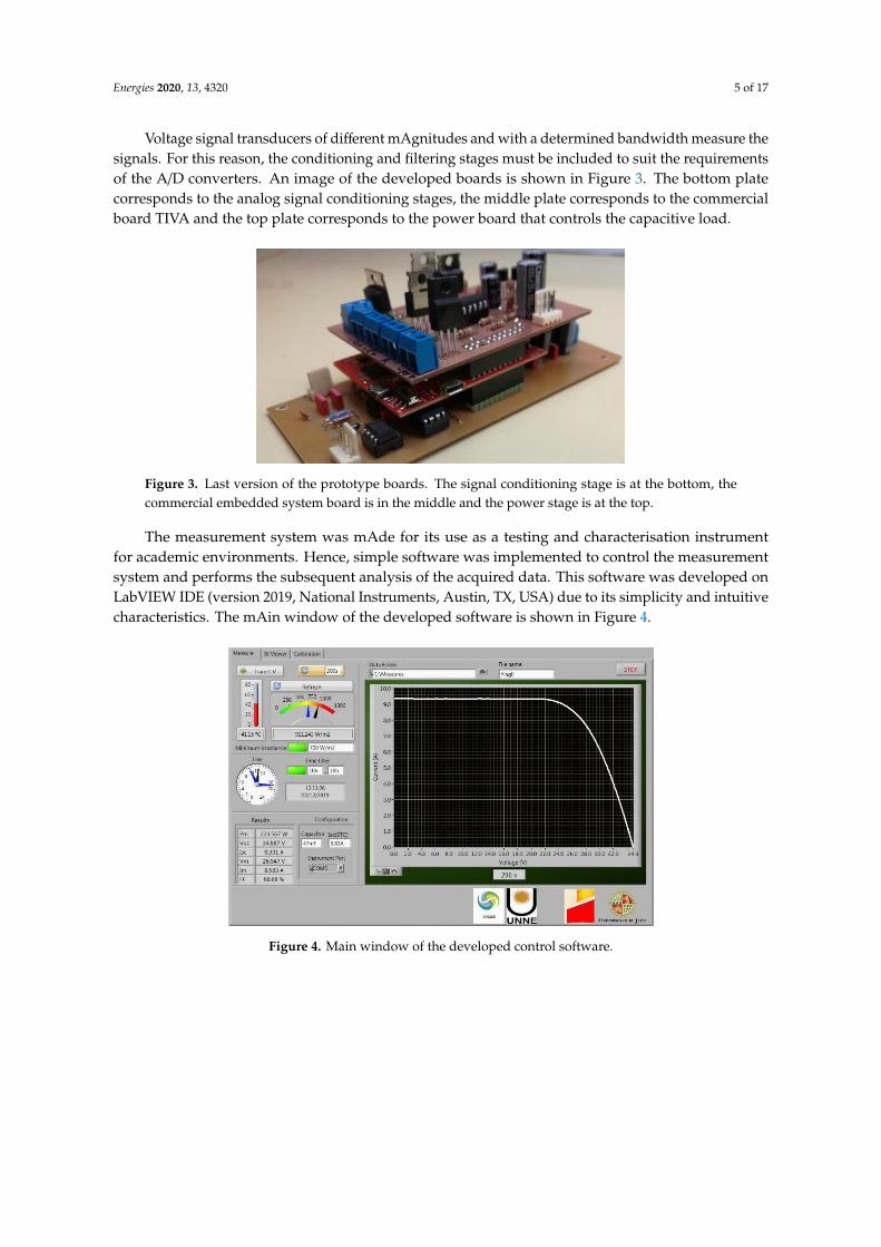
Voltage signal transducers of different mAgnitudes and with a determined bandwidth measure thesignals. For this reason, the conditioning and filtering stages must be included to suit the requirementsof the A/D converters. An image of the developed boards is shown in Figure 3. The bottom platecorresponds to the analog signal conditioning stages, the middle plate corresponds to the commercialboard TIVA and the top plate corresponds to the power board that controls the capacitive load.
Figure 3. Last version of the prototype boards. The signal conditioning stage is at the bottom, thecommercial embedded system board is in the middle and the power stage is at the top.
The measurement system was mAde for its use as a testing and characterisation instrumentfor academic environments. Hence, simple software was implemented to control the measurementsystem and performs the subsequent analysis of the acquired data. This software was developed onLabVIEW IDE (version 2019, National Instruments, Austin, TX, USA) due to its simplicity and intuitivecharacteristics. The mAin window of the developed software is shown in Figure 4.
Figure 4. Main window of the developed control software.
Energies 2020, 13, 4320 6 of 17
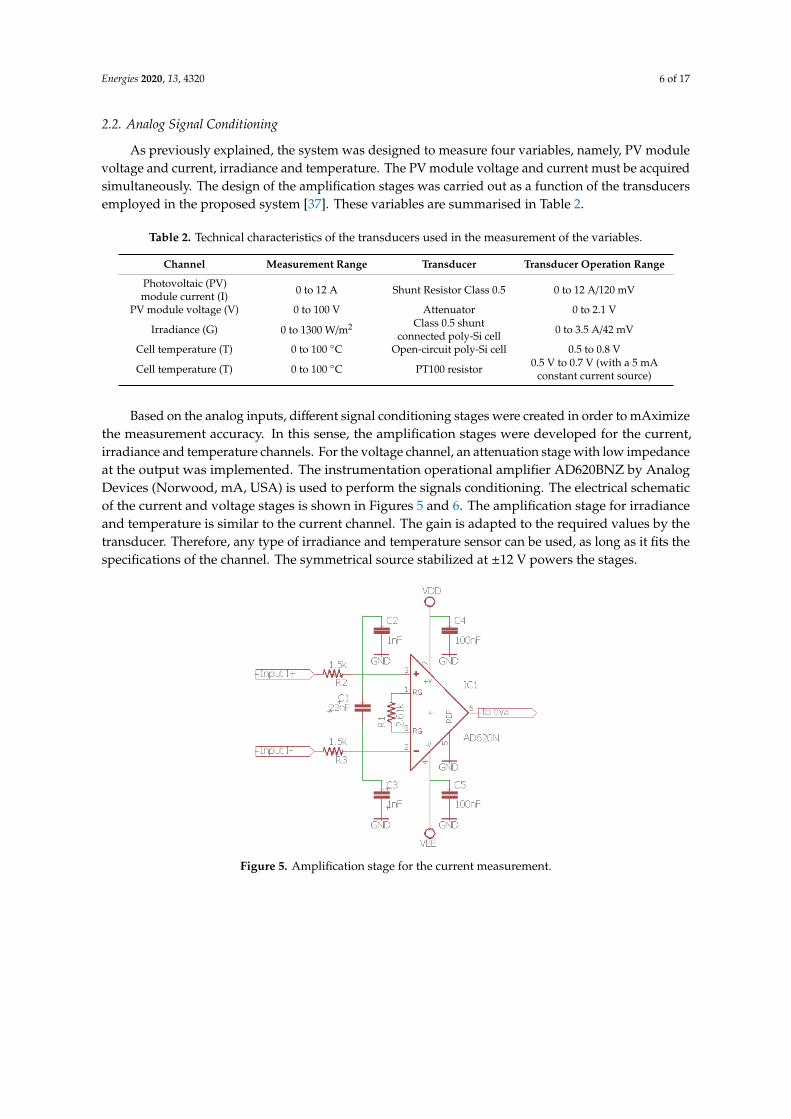
2.2. Analog Signal Conditioning
As previously explained, the system was designed to measure four variables, namely, PV modulevoltage and current, irradiance and temperature. The PV module voltage and current must be acquiredsimultaneously. The design of the amplification stages was carried out as a function of the transducersemployed in the proposed system [37]. These variables are summarised in Table 2.
Table 2. Technical characteristics of the transducers used in the measurement of the variables.
Channel Measurement Range Transducer Transducer Operation Range
Photovoltaic (PV)module current (I) 0 to 12 A Shunt Resistor Class 0.5 0 to 12 A/120 mV
PV module voltage (V) 0 to 100 V Attenuator 0 to 2.1 V
Irradiance (G) 0 to 1300 W/m2 Class 0.5 shuntconnected poly-Si cell 0 to 3.5 A/42 mV
Cell temperature (T) 0 to 100 C Open-circuit poly-Si cell 0.5 to 0.8 V
Cell temperature (T) 0 to 100 C PT100 resistor 0.5 V to 0.7 V (with a 5 mAconstant current source)
Based on the analog inputs, different signal conditioning stages were created in order to mAximizethe measurement accuracy. In this sense, the amplification stages were developed for the current,irradiance and temperature channels. For the voltage channel, an attenuation stage with low impedanceat the output was implemented. The instrumentation operational amplifier AD620BNZ by AnalogDevices (Norwood, mA, USA) is used to perform the signals conditioning. The electrical schematicof the current and voltage stages is shown in Figures 5 and 6. The amplification stage for irradianceand temperature is similar to the current channel. The gain is adapted to the required values by thetransducer. Therefore, any type of irradiance and temperature sensor can be used, as long as it fits thespecifications of the channel. The symmetrical source stabilized at ±12 V powers the stages.
Figure 5. Amplification stage for the current measurement.
Energies 2020, 13, 4320 7 of 17
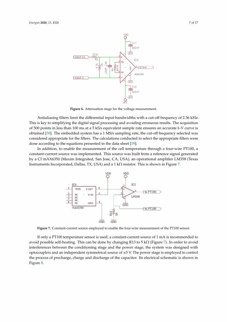
Figure 6. Attenuation stage for the voltage measurement.
Antialiasing filters limit the differential input bandwidths with a cut-off frequency of 2.36 kHz.This is key to simplifying the digital signal processing and avoiding erroneous results. The acquisitionof 500 points in less than 100 ms at a 5 kS/s equivalent sample rate ensures an accurate I–V curve isobtained [38]. The embedded system has a 1 MS/s sampling rate, the cut-off frequency selected wasconsidered appropriate for the filters. The calculations conducted to select the appropriate filters weredone according to the equations presented in the data sheet [39].
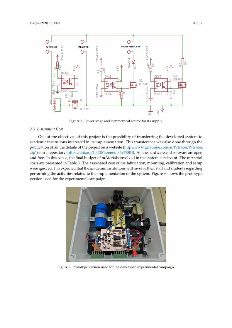
In addition, to enable the measurement of the cell temperature through a four-wire PT100, aconstant-current source was implemented. This source was built from a reference signal generatedby a CI mAX6350 (Maxim Integrated, San Jose, CA, USA), an operational amplifier LM358 (TexasInstruments Incorporated, Dallas, TX, USA) and a 1 kΩ resistor. This is shown in Figure 7.
Figure 7. Constant-current source employed to enable the four-wire measurement of the PT100 sensor.
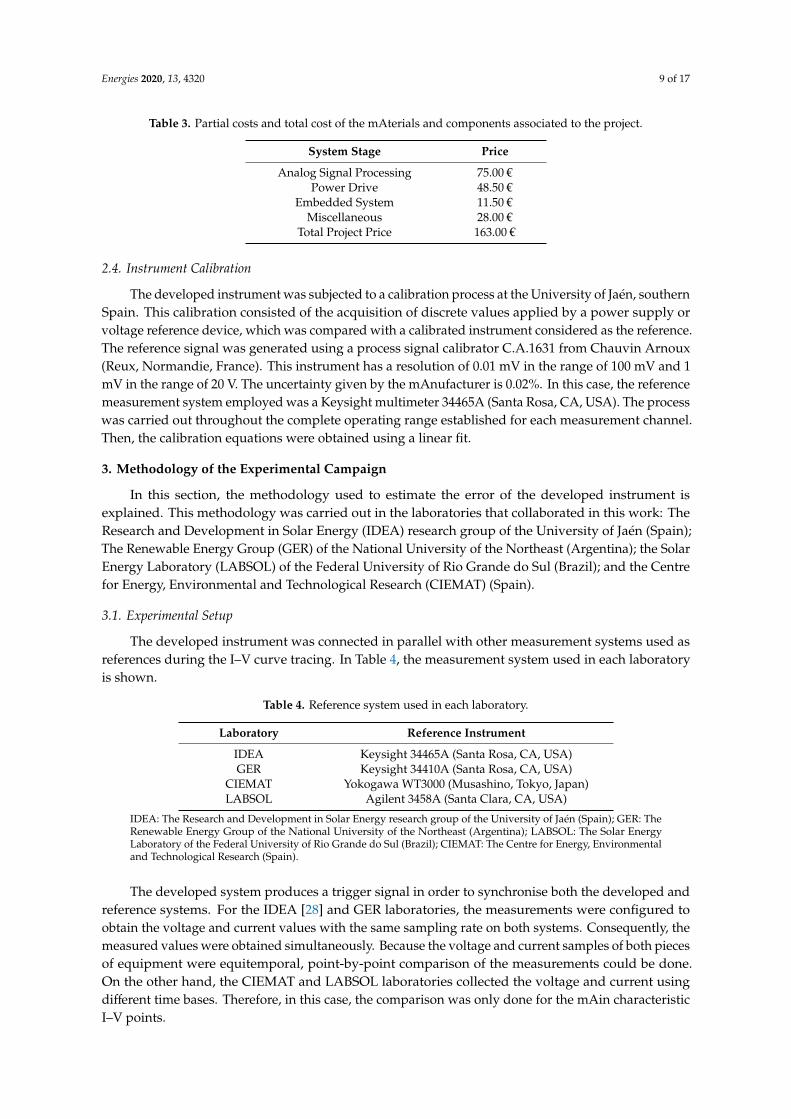
If only a PT100 temperature sensor is used, a constant-current source of 1 mA is recommended toavoid possible self-heating. This can be done by changing R13 to 5 kΩ (Figure 7). In order to avoidinterferences between the conditioning stage and the power stage, the system was designed withoptocouplers and an independent symmetrical source of ±5 V. The power stage is employed to controlthe process of precharge, charge and discharge of the capacitor. Its electrical schematic is shown inFigure 8.
Energies 2020, 13, 4320 8 of 17
Figure 8. Power stage and symmetrical source for its supply.
2.3. Instrument Cost
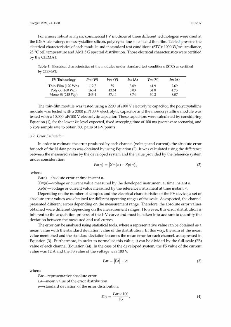
One of the objectives of this project is the possibility of transferring the developed system toacademic institutions interested in its implementation. This transference was also done through thepublication of all the details of the project on a website (http://www.ger-unne.com.ar/IVtracer/IVtracer.zip) or in a repository (https://doi.org/10.5281/zenodo.3959804). All the hardware and software are openand free. In this sense, the final budget of mAterials involved in the system is relevant. The mAterialcosts are presented in Table 3. The associated cost of the fabrication, mounting, calibration and setupwere ignored. It is expected that the academic institutions will involve their staff and students regardingperforming the activities related to the implementation of the system. Figure 9 shows the prototypeversion used for the experimental campaign.
Figure 9. Prototype version used for the developed experimental campaign.
Energies 2020, 13, 4320 9 of 17
Table 3. Partial costs and total cost of the mAterials and components associated to the project.
System Stage Price
Analog Signal Processing 75.00 €Power Drive 48.50 €
Embedded System 11.50 €Miscellaneous 28.00 €
Total Project Price 163.00 €
2.4. Instrument Calibration
The developed instrument was subjected to a calibration process at the University of Jaén, southernSpain. This calibration consisted of the acquisition of discrete values applied by a power supply orvoltage reference device, which was compared with a calibrated instrument considered as the reference.The reference signal was generated using a process signal calibrator C.A.1631 from Chauvin Arnoux(Reux, Normandie, France). This instrument has a resolution of 0.01 mV in the range of 100 mV and 1mV in the range of 20 V. The uncertainty given by the mAnufacturer is 0.02%. In this case, the referencemeasurement system employed was a Keysight multimeter 34465A (Santa Rosa, CA, USA). The processwas carried out throughout the complete operating range established for each measurement channel.Then, the calibration equations were obtained using a linear fit.
3. Methodology of the Experimental Campaign
In this section, the methodology used to estimate the error of the developed instrument isexplained. This methodology was carried out in the laboratories that collaborated in this work: TheResearch and Development in Solar Energy (IDEA) research group of the University of Jaén (Spain);The Renewable Energy Group (GER) of the National University of the Northeast (Argentina); the SolarEnergy Laboratory (LABSOL) of the Federal University of Rio Grande do Sul (Brazil); and the Centrefor Energy, Environmental and Technological Research (CIEMAT) (Spain).
3.1. Experimental Setup
The developed instrument was connected in parallel with other measurement systems used asreferences during the I–V curve tracing. In Table 4, the measurement system used in each laboratoryis shown.
Table 4. Reference system used in each laboratory.
Laboratory Reference Instrument
IDEA Keysight 34465A (Santa Rosa, CA, USA)GER Keysight 34410A (Santa Rosa, CA, USA)
CIEMAT Yokogawa WT3000 (Musashino, Tokyo, Japan)LABSOL Agilent 3458A (Santa Clara, CA, USA)
IDEA: The Research and Development in Solar Energy research group of the University of Jaén (Spain); GER: TheRenewable Energy Group of the National University of the Northeast (Argentina); LABSOL: The Solar EnergyLaboratory of the Federal University of Rio Grande do Sul (Brazil); CIEMAT: The Centre for Energy, Environmentaland Technological Research (Spain).
The developed system produces a trigger signal in order to synchronise both the developed andreference systems. For the IDEA [28] and GER laboratories, the measurements were configured toobtain the voltage and current values with the same sampling rate on both systems. Consequently, themeasured values were obtained simultaneously. Because the voltage and current samples of both piecesof equipment were equitemporal, point-by-point comparison of the measurements could be done.On the other hand, the CIEMAT and LABSOL laboratories collected the voltage and current usingdifferent time bases. Therefore, in this case, the comparison was only done for the mAin characteristicI–V points.
Energies 2020, 13, 4320 10 of 17
For a more robust analysis, commercial PV modules of three different technologies were used atthe IDEA laboratory: monocrystalline silicon, polycrystalline silicon and thin film. Table 5 presents theelectrical characteristics of each module under standard test conditions (STC): 1000 W/m2 irradiance,25 C cell temperature and AM1.5 G spectral distribution. Those electrical characteristics were certifiedby the CIEMAT.
Table 5. Electrical characteristics of the modules under standard test conditions (STC) as certifiedby CIEMAT.
PV Technology Pm (W) Voc (V) Isc (A) Vm (V) Im (A)
Thin-Film (120 Wp) 112.7 59 3.09 41.9 2.69Poly-Si (160 Wp) 165.4 43.61 5.03 34.8 4.75
Mono-Si (245 Wp) 243.4 37.44 8.74 30.2 8.07
The thin-film module was tested using a 2200 µF/100 V electrolytic capacitor, the polycrystallinemodule was tested with a 3300 µF/100 V electrolytic capacitor and the monocrystalline module wastested with a 10,000 µF/100 V electrolytic capacitor. These capacitors were calculated by consideringEquation (1), for the lower Isc level expected, fixed sweeping time of 100 ms (worst-case scenario), and5 kS/s sample rate to obtain 500 pairs of I-V points.
3.2. Error Estimation
In order to estimate the error produced by each channel (voltage and current), the absolute errorfor each of the N data pairs was obtained by using Equation (2). It was calculated using the differencebetween the measured value by the developed system and the value provided by the reference systemunder consideration:
Ea(n) =∣∣∣Xm(n) −Xp(n)
∣∣∣, (2)
where:Ea(n)—absolute error at time instant n.Xm(n)—voltage or current value measured by the developed instrument at time instant n.Xp(n)—voltage or current value measured by the reference instrument at time instant n.Depending on the number of samples and the electrical characteristics of the PV device, a set of
absolute error values was obtained for different operating ranges of the scale. As expected, the channelpresented different errors depending on the measurement range. Therefore, the absolute error valuesobtained were different depending on the measurement ranges. However, this error distribution isinherent to the acquisition process of the I–V curve and must be taken into account to quantify thedeviation between the measured and real curves.
The error can be analysed using statistical tools, where a representative value can be obtained as amean value with the standard deviation value of the distribution. In this way, the sum of the meanvalue mentioned and the standard deviation becomes the mean error for each channel, as expressed inEquation (3). Furthermore, in order to normalise this value, it can be divided by the full-scale (FS)value of each channel (Equation (4)). In the case of the developed system, the FS value of the currentvalue was 12 A and the FS value of the voltage was 100 V.
Ear =∣∣∣Ea∣∣∣+ |σ| (3)
where:Ear—representative absolute error.Ea—mean value of the error distribution.σ—standard deviation of the error distribution.
E% =Ear× 100
FS, (4)
Energies 2020, 13, 4320 11 of 17
where:E%—normalized percentage error.FS—full-scale value.Both the voltage and current are involved in the measurement of the I–V curve. The multiplication
of these values represents the power of the PV module. As proposed in the data sheet [39], to estimatethe error committed by the instrument on the acquisition of the power [40], the sum of the normalisedpercentage error of each channel was done by using Equation (5):
EP% = EV% + EI% (5)
where:EP%—percentage error in the acquisition of the power.EV%—percentage error in the voltage channel.EI%—percentage error in the current channel.In this way, it is possible to obtain a unique value that represents the error of the acquisition of the
I–V curve.
4. Results
In this section, first, the results obtained from the experimental campaign carried out at the IDEAlaboratories are presented. This data set represents the experimental campaign that involved thelargest number of PV technologies and in which the I–V curves were measured at the same samplingrate. More than 50 curves were obtained for each PV module. In all the performed tests, the mAximumsolar irradiance uncertainty provided by the sensor was 2.0% and the mAximum relative differenceobtained between the reference system and the prototype was lower than 0.5%.
The results include the power percentage error (EP%), the percentage error in the voltage channel(EV%) and the percentage error in the current channel (EI%). These mAgnitudes were evaluated as afunction of the irradiance since this was the most relevant parameter for defining the output of thePV technology.
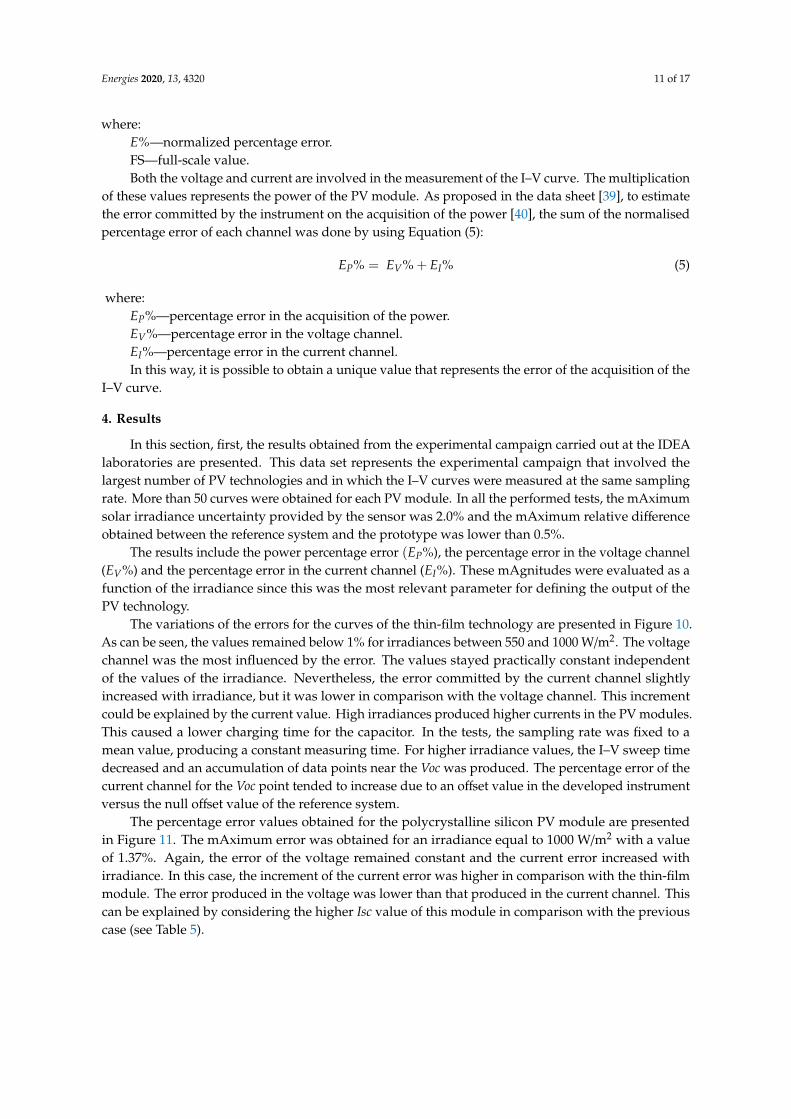
The variations of the errors for the curves of the thin-film technology are presented in Figure 10.As can be seen, the values remained below 1% for irradiances between 550 and 1000 W/m2. The voltagechannel was the most influenced by the error. The values stayed practically constant independentof the values of the irradiance. Nevertheless, the error committed by the current channel slightlyincreased with irradiance, but it was lower in comparison with the voltage channel. This incrementcould be explained by the current value. High irradiances produced higher currents in the PV modules.This caused a lower charging time for the capacitor. In the tests, the sampling rate was fixed to amean value, producing a constant measuring time. For higher irradiance values, the I–V sweep timedecreased and an accumulation of data points near the Voc was produced. The percentage error of thecurrent channel for the Voc point tended to increase due to an offset value in the developed instrumentversus the null offset value of the reference system.
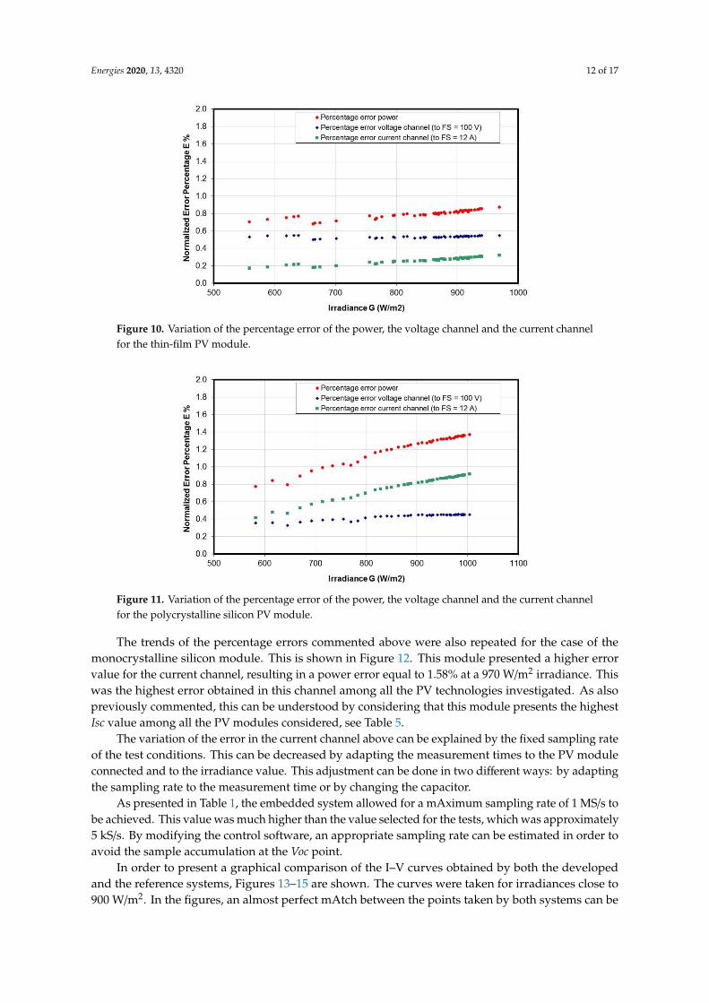
The percentage error values obtained for the polycrystalline silicon PV module are presentedin Figure 11. The mAximum error was obtained for an irradiance equal to 1000 W/m2 with a valueof 1.37%. Again, the error of the voltage remained constant and the current error increased withirradiance. In this case, the increment of the current error was higher in comparison with the thin-filmmodule. The error produced in the voltage was lower than that produced in the current channel. Thiscan be explained by considering the higher Isc value of this module in comparison with the previouscase (see Table 5).
Energies 2020, 13, 4320 12 of 17
Figure 10. Variation of the percentage error of the power, the voltage channel and the current channelfor the thin-film PV module.
Figure 11. Variation of the percentage error of the power, the voltage channel and the current channelfor the polycrystalline silicon PV module.
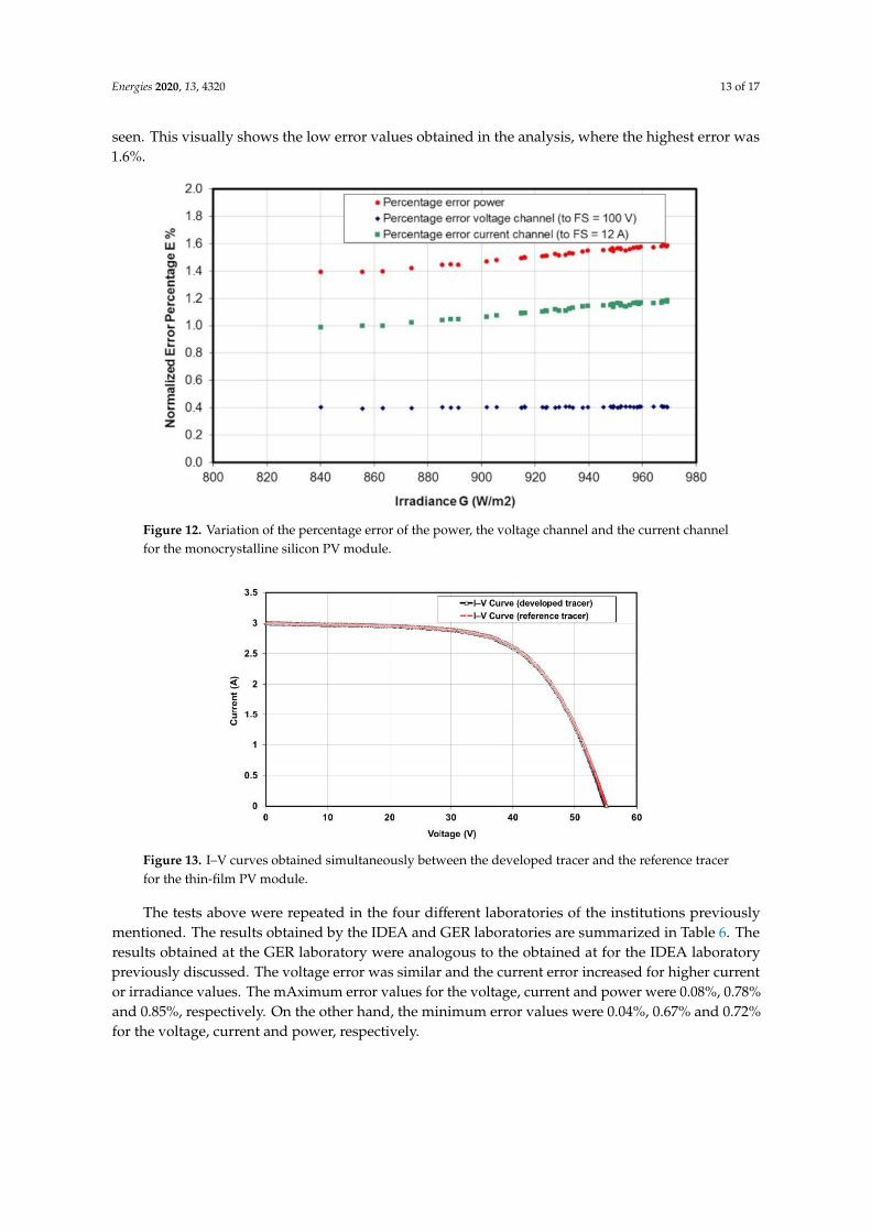
The trends of the percentage errors commented above were also repeated for the case of themonocrystalline silicon module. This is shown in Figure 12. This module presented a higher errorvalue for the current channel, resulting in a power error equal to 1.58% at a 970 W/m2 irradiance. Thiswas the highest error obtained in this channel among all the PV technologies investigated. As alsopreviously commented, this can be understood by considering that this module presents the highestIsc value among all the PV modules considered, see Table 5.
The variation of the error in the current channel above can be explained by the fixed sampling rateof the test conditions. This can be decreased by adapting the measurement times to the PV moduleconnected and to the irradiance value. This adjustment can be done in two different ways: by adaptingthe sampling rate to the measurement time or by changing the capacitor.
As presented in Table 1, the embedded system allowed for a mAximum sampling rate of 1 MS/s tobe achieved. This value was much higher than the value selected for the tests, which was approximately5 kS/s. By modifying the control software, an appropriate sampling rate can be estimated in order toavoid the sample accumulation at the Voc point.
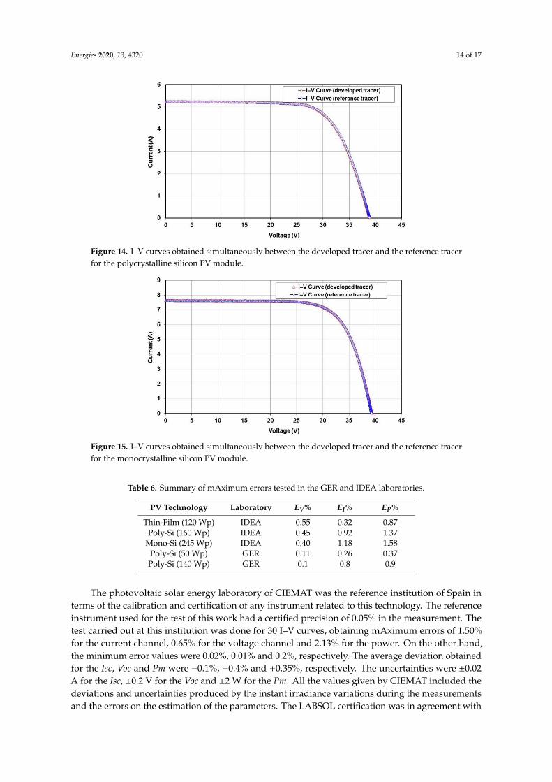
In order to present a graphical comparison of the I–V curves obtained by both the developedand the reference systems, Figures 13–15 are shown. The curves were taken for irradiances close to900 W/m2. In the figures, an almost perfect mAtch between the points taken by both systems can be
Energies 2020, 13, 4320 13 of 17
seen. This visually shows the low error values obtained in the analysis, where the highest error was1.6%.
Figure 12. Variation of the percentage error of the power, the voltage channel and the current channelfor the monocrystalline silicon PV module.
Figure 13. I–V curves obtained simultaneously between the developed tracer and the reference tracerfor the thin-film PV module.
The tests above were repeated in the four different laboratories of the institutions previouslymentioned. The results obtained by the IDEA and GER laboratories are summarized in Table 6. Theresults obtained at the GER laboratory were analogous to the obtained at for the IDEA laboratorypreviously discussed. The voltage error was similar and the current error increased for higher currentor irradiance values. The mAximum error values for the voltage, current and power were 0.08%, 0.78%and 0.85%, respectively. On the other hand, the minimum error values were 0.04%, 0.67% and 0.72%for the voltage, current and power, respectively.
Energies 2020, 13, 4320 14 of 17
Figure 14. I–V curves obtained simultaneously between the developed tracer and the reference tracerfor the polycrystalline silicon PV module.
Figure 15. I–V curves obtained simultaneously between the developed tracer and the reference tracerfor the monocrystalline silicon PV module.
Table 6. Summary of mAximum errors tested in the GER and IDEA laboratories.
PV Technology Laboratory EV% EI% EP%
Thin-Film (120 Wp) IDEA 0.55 0.32 0.87Poly-Si (160 Wp) IDEA 0.45 0.92 1.37
Mono-Si (245 Wp) IDEA 0.40 1.18 1.58Poly-Si (50 Wp) GER 0.11 0.26 0.37Poly-Si (140 Wp) GER 0.1 0.8 0.9
The photovoltaic solar energy laboratory of CIEMAT was the reference institution of Spain interms of the calibration and certification of any instrument related to this technology. The referenceinstrument used for the test of this work had a certified precision of 0.05% in the measurement. Thetest carried out at this institution was done for 30 I–V curves, obtaining mAximum errors of 1.50%for the current channel, 0.65% for the voltage channel and 2.13% for the power. On the other hand,the minimum error values were 0.02%, 0.01% and 0.2%, respectively. The average deviation obtainedfor the Isc, Voc and Pm were −0.1%, −0.4% and +0.35%, respectively. The uncertainties were ±0.02A for the Isc, ±0.2 V for the Voc and ±2 W for the Pm. All the values given by CIEMAT included thedeviations and uncertainties produced by the instant irradiance variations during the measurementsand the errors on the estimation of the parameters. The LABSOL certification was in agreement with
Energies 2020, 13, 4320 15 of 17
these results and showed similar error ranges. The results showed an average deviation of 0.58%,0.23% and 0.05% in the estimation of the Isc, Voc and Pm, respectively.
5. Conclusions
An I–V tracer for testing PV modules under real operating conditions was developed and presented.The equipment had a high degree of accuracy at a very low cost and a budget lower than 170 €. Fourinstitutions were involved in the experimental campaign conducted to check the quality of the newdevice. Three PV modules from different technologies (monocrystalline silicon, polycrystalline siliconand thin-film) were tested. The obtained statistical error of the acquisition of the I–V curve was foundto be lower than 1.6% when compared to commercial instruments. This error could be lowered infuture work by modifying the control software to adapt the sampling rate as a function of the PVmodule characteristics and the irradiance and temperature test conditions. The CIEMAT laboratoryhad certified average deviations lower than 0.4%. The system can be implemented without the needfor expensive instruments, ensuring access to the technology for the purpose of learning PV technology.All the source files to replicate the prototype presented in this work can be obtained at the followinglinks: http://www.ger-unne.com.ar/IVtracer/IVtracer.zip or https://doi.org/10.5281/zenodo.3959804.
Author Contributions: All authors have contributed actively to the work that has resulted in this paper. M.C., A.F.and J.M.-R. wrote the paper. M.C. and J.M.-R. built and tested the prototype. J.M.-R. and A.R.G.M. performed theexperiments. M.C., A.F. and J.d.l.C.H. conceived the idea and design of the device. J.d.l.C.H. and E.F.F. suggestedand revised the scientific procedure. J.d.l.C.H, E.F.F. and L.H.V. revised the paper and provided suggestionsregarding the implementation and validation of the electronic device. All authors have read and agreed to thepublished version of the manuscript.
Funding: This work has been supported by the Andalusian International Cooperation Agency (Agencia Andaluzade Cooperación Internacional para el Desarrollo (AACID)) in the framework of the project: “Emergiendo con el sol.Apoyo institucional al centro de energías renovables de la Universidad Nacional de Ingeniería en el campo de lageneración de energía eléctrica empleando tecnología fotovoltaica” (Emerging with the sun. Institutional supportto the renewable energy center of the National University of Engineering in the field of electricity generationusing photovoltaic technology) and “Plan Plurianual de I+D” (Pluriannual R&D Plan) from “Centro de EstudiosAvanzados en Energía y Medio Ambiente” (Centre of Advanced Studies in Energy and Environment) of theUniversity of Jaen in the framework of the project: “Acciones de cooperación al desarrollo en el mArco de latransferencia del conocimiento a universidades iberoamericanas. Caso de estudio: caracterización a sol real demódulos FV utilizando equipamiento de bajo coste” (Development cooperation actions in the framework ofknowledge transfer to Ibero-American universities. Study case: real sun characterization of PV modules usinglow-cost equipment).
Acknowledgments: The authors would like to thank the laboratory staff from the LABSOL laboratory in Braziland the CIEMAT staff in Spain for their collaboration in the experiments carried out in the project presented inthis article.
Conflicts of Interest: The authors declare no conflict of interest.
References
1. Ellabban, O.; Abu-Rub, H.; Blaabjerg, F. Renewable energy resources: Current status, future prospects andtheir enabling technology. Renew. Sustain. Energy Rev. 2014, 39, 748–764. [CrossRef]
2. Alonso, M.; Amaris, H.; Alvarez-Ortega, C. Integration of renewable energy sources in smart grids by meansof evolutionary optimization algorithms. Expert Syst. Appl. 2012, 39, 5513–5522. [CrossRef]
3. Bayod-Rújula, A.A. Future development of the electricity systems with distributed generation. Energy 2009,34, 377–383. [CrossRef]
4. Adinolfi, G.; Graditi, G.; Siano, P.; Piccolo, A. Multiobjective Optimal Design of Photovoltaic SynchronousBoost Converters Assessing Efficiency, Reliability, and Cost Savings. IEEE Trans. Ind. Informatics 2015, 11,1038–1048. [CrossRef]
5. Denholm, P.; mArgolis, R.M. Evaluating the limits of solar photovoltaics (PV) in traditional electric powersystems. Energy Policy 2007, 35, 2852–2861. [CrossRef]
6. International Electrotechnical Commission. EN 61646:2008. Thin-Film Terrestrial Photovoltaic (PV)Modules—Design Qualification and Type Approval; International Electrotechnical Commission: Geneva,Switzerland, 2008.

Energies 2020, 13, 4320 16 of 17
7. International Electrotechnical Commission. IEC 60904-1, Photovoltaic Devices, Part 1: Measurement ofPhotovoltaic Current–Voltage Characteristics; International Electrotechnical Commission: Geneva, Switzerland,2006.
8. Muñoz, J.V.; Nofuentes, G.; Fuentes, M.; de la Casa, J.; Aguilera, J. DC energy yield prediction in largemonocrystalline and polycrystalline PV plants: Time-domain integration of Osterwald’s model. Energy 2016,114, 951–960. [CrossRef]
9. Schuss, C.; Leppänen, K.; Remes, K.; Saarela, J.; Fabritius, T.; Eichberger, B.; Rahkonen, T. Detecting Defectsin Photovoltaic Cells and Panels and Evaluating the Impact on Output Performances. IEEE Trans. Instrum.Meas. 2016, 65, 1108–1119. [CrossRef]
10. Almonacid, F.; Fernández, E.F.; mAllick, T.K.; Pérez-Higueras, P.J. High concentrator photovoltaic modulesimulation by neuronal networks using spectrally corrected direct normal irradiance and cell temperature.Energy 2015, 84, 336–343. [CrossRef]
11. Gasparin, F.P.; Bühler, A.J.; Rampinelli, G.A.; Krenzinger, A. Statistical analysis of I–V curve parameters fromphotovoltaic modules. Sol. Energy 2016, 131, 30–38. [CrossRef]
12. Montes-Romero, J.; Almonacid, F.; Theristis, M.; de la Casa, J.; Georghiou, G.E.; Fernández, E.F. Comparativeanalysis of parameter extraction techniques for the electrical characterization of multi-junction CPV andm-Si technologies. Sol. Energy 2018, 160, 275–288. [CrossRef]
13. Luque, A.; Hegedus, S. Handbook of Photovoltaic Science and Engineering; Wiley: Hoboken, NJ, USA, 2003;ISBN 0471491969.
14. Abbassi, A.; Gammoudi, R.; Dami, M.A.; Hasnaoui, O.; Jemli, M. An improved single-diode model parametersextraction at different operating conditions with a view to modeling a photovoltaic generator: A comparativestudy. Sol. Energy 2017, 155, 478–489. [CrossRef]
15. Ishaque, K.; Salam, Z.; Taheri, H. Simple, fast and accurate two-diode model for photovoltaic modules. Sol.Energy mAter. Sol. Cells 2011, 95, 586–594. [CrossRef]
16. Celik, A.N.; Acikgoz, N. Modelling and experimental verification of the operating current of mono-crystallinephotovoltaic modules using four- and five-parameter models. Appl. Energy 2007, 84, 1–15. [CrossRef]
17. Attivissimo, F.; Di Nisio, A.; Savino, M.; Spadavecchia, M. Uncertainty analysis in photovoltaic cell parameterestimation. IEEE Trans. Instrum. Meas. 2012, 61, 1334–1342. [CrossRef]
18. Willoughby, A.A.; Osinowo, M.O. Development of an electronic load I-V curve tracer to investigate theimpact of Harmattan aerosol loading on PV module pern2tkformance in southwest Nigeria. Sol. Energy2018, 166, 171–180. [CrossRef]
19. Vega, A.; Valiño, V.; Conde, E.; Ramos, A.; Reina, P. Double sweep tracer for I-V curves characterization andcontinuous monitoring of photovoltaic facilities. Sol. Energy 2019, 190, 622–629. [CrossRef]
20. Sánchez-Pacheco, F.J.; Sotorrío-Ruiz, P.J.; Heredia-Larrubia, J.R.; Pérez-Hidalgo, F.; De Cardona, M.S.PLC-based PV plants smart monitoring system: Field measurements and uncertainty estimation. IEEE Trans.Instrum. Meas. 2014, 63, 2215–2222. [CrossRef]
21. Zhu, Y.; Xiao, W. A comprehensive review of topologies for photovoltaic I–V curve tracer. Sol. Energy 2020,196, 346–357. [CrossRef]
22. Chen, Z.; Lin, W.; Wu, L.; Long, C.; Lin, P.; Cheng, S. A capacitor based fast I-V characteristics tester forphotovoltaic arrays. Energy Procedia 2018, 145, 381–387. [CrossRef]
23. Amiry, H.; Benhmida, M.; Bendaoud, R.; Hajjaj, C.; Bounouar, S.; Yadir, S.; Raïs, K.; Sidki, M. Design andimplementation of a photovoltaic I-V curve tracer: Solar modules characterization under real operatingconditions. Energy Convers. mAnag. 2018, 169, 206–216. [CrossRef]
24. Leite, V.; Chenlo, F. An improved electronic circuit for tracing the IV characteristics of photovoltaic modulesand strings. In Proceedings of the International Conference on Renewable Energies and Power Quality,Granada, Spain, 23–25 mArch 2010; Volume 1, pp. 1224–1228.
25. García-Valverde, R.; Chaouki-Almagro, S.; Corazza, M.; Espinosa, N.; Hösel, M.; Søndergaard, R.R.;Jørgensen, M.; Villarejo, J.A.; Krebs, F.C. Portable and wireless IV-curve tracer for >5 kV organic photovoltaicmodules. Sol. Energy mAter. Sol. Cells 2016, 151, 60–65. [CrossRef]
26. Leite, V.; Batista, J.; Chenlo, F.; Afonso, J.L. Low-Cost I-V Tracer for Photovoltaic Modules and Strings.In Proceedings of the International Symposium on Power Electronics, Electrical Drives, Automation andMotion, Naples, Italy, 18–20 June 2014.
Energies 2020, 13, 4320 17 of 17
27. Papageorgas, P.; Piromalis, D.; Valavanis, T.; Kambasis, S.; Iliopoulou, T.; Vokas, G. A low-cost and fast PVI-V curve tracer based on an open source platform with M2M communication capabilities for preventivemonitoring. Energy Procedia 2015, 74, 423–438. [CrossRef]
28. Montes-Romero, J.; Piliougine, M.; Muñoz, J.; Fernández, E.; de la Casa, J. Photovoltaic Device PerformanceEvaluation Using an Open-Hardware System and Standard Calibrated Laboratory Instruments. Energies2017, 10, 1869. [CrossRef]
29. Spertino, F.; Ahmad, J.; Ciocia, A.; Di Leo, P.; Murtaza, A.F.; Chiaberge, M. Capacitor charging method forI–V curve tracer and MPPT in photovoltaic systems. Sol. Energy 2015, 119, 461–473. [CrossRef]
30. Blaesser, G.; Munro, D. Guidelines for the assessment of photovoltaic plants. In Document C: Initial andPeriodic Test on Photovoltaic Plants; Europeean Commission Joint Research Centre: Ispra, Italy, 1995.
31. Duran, E.; Piliougine, M.; De Cardona, M.S.; Galan, J.; Andujar, J.M. Different methods to obtain the I-V curveof PV modules: A review. In Proceedings of the Conference Record of the IEEE Photovoltaic, San Diego, CA,USA, 11–16 mAy 2008.
32. Di Nisio, A.; Di Noia, T.; Carducci, C.G.C.; Spadavecchia, M. High dynamic range power consumptionmeasurement in microcontroller-based applications. IEEE Trans. Instrum. Meas. 2016, 65, 1968–1976.[CrossRef]
33. Firman, A.; Zini, L.; Sanchez, R.; Vera, L. Desarrollo y calibración de dispositivos fotovoltaicos para determinarel recurso solar utilizable por sfcr. Av. Energías Renov. Medio Ambient. 2014, 18, 9–17.
34. Almonacid, F.; Rodrigo, P.; Fernández, E.F. Determination of the current–voltage characteristics of concentratorsystems by using different adapted conventional techniques. Energy 2016, 101, 146–160. [CrossRef]
35. Salvadori, F.; Gehrke, C.S.; Hartmann, L.V.; mAcedo, E.T.; de Lima, A.L.; mAia, S.L. Design of an intelligentelectronic device based on TivaC platform for smart grid applications. In Proceedings of the 2016 IEEEInternational Instrumentation and Measurement Technology Conference Proceedings, Taiwan, 23–26 mAy2016; pp. 1–6.
36. Texas Instruments. Tiva TM4C123GH6PM Microcontroller Data Sheet; Texas Instruments Incorporated: Dallas,TX, USA, 2014.
37. Giordani, A.; mAri, L. Measurement, Models, and Uncertainty. IEEE Trans. Instrum. Meas. 2012, 61,2144–2152. [CrossRef]
38. Martínez-Moreno, F.; Lorenzo, E.; Muñoz, J.; Moretón, R. On the testing of large PV arrays. Prog. Photovolt.Res. Appl. 2011, 15, 659–676. [CrossRef]
39. Kitchin, C.; Counts, L. Analog Devices Instrumentation Amplifier AD620; Analog Devices: Norwood, mA, USA,2011.
40. Taylor, J.R. Introduction To Error Analysis: The Study of Uncertainties in Physical Measurements;ASMSU/Spartans.4.Spartans Textbook; University Science Books: Mill Valley, CA, USA, 1997;ISBN 9780935702750.
© 2020 by the authors. Licensee MDPI, Basel, Switzerland. This article is an open accessarticle distributed under the terms and conditions of the Creative Commons Attribution(CC BY) license (http://creativecommons.org/licenses/by/4.0/).


![[Photovoltaic modules (PV modules) – Universal Waste ... · 2/10/2019 · [Photovoltaic modules (PV modules) – Universal Waste Management ] Proposed Regulation Text R-2017-04](https://img.pdfslide.net/doc/110x75/5f4ce3b243e16749da1b123d/photovoltaic-modules-pv-modules-a-universal-waste-2102019-photovoltaic.jpg)