Embed Size (px)
Citation preview
© 2014 IJEDR | Volume 2, Issue 1 | ISSN: 2321-9939
IJEDR1401111 International Journal of Engineering Development and Research (www.ijedr.org) 615
Low Noise Amplifier Design for Navigation
Signal Receiver
1Nimesh M. Prabhakar,
2A K. Sisodia
1Department of Master of E.C Engineering,
2 Associated proffecer
LJIET, Gujarat Technological University-Ahmedabad [email protected],
Abstract - This paper presents the design and simulation of a 1.1 GHz and 2.5 GHz front end low noise amplifier for
navigation signal receiving .This low noise amplifier (LNA) is design for application of receiving a signal of Indian
regional navigation satellite system (IRNSS). This amplifier uses NXP’s BFU730LX which is a low noise and high dynamic
range bipolar junction transistor(BJT).The key points are analysis device's stability with Stability factor and the input
and output impedance matching with Smith Chart and Tuning. Finally, the performance parameters of LNA were
obtained with the simulation of S parameters. The simulation has been performed using Advanced Design System (ADS)
2011.10 simulation software.
Keywords - low noise amplifier (LNA); ADS software; noise figure; optimization design
I. INTRODUCTION
The Indian Regional Navigational Satellite System (IRNSS) is an autonomous regional satellite navigation system being
developed by Indian Space Research Organization (ISRO) which would be under the total control of Indian government .This
Navigation Satellite System Is Different from Other Satellite System Because IRNSS operates on both L band (1176 MHz) and S
band (2492.08 MHz).In Navigation System First time S band are use. Design of LNA is really a critical issue is to design and
develop the LNA, working on both L band and S band. Low-Noise Amplifiers are key components in the receiving end of nearly
every communications system. The wanted input signal of these systems is usually very weak and the primary purpose of the
LNA is consequently to amplify the signal while at the same time adding as little additional noise as possible. Its performance is
measured with parameter such as noise figures, gain, return loss and stability for getting the optimum performance.
II. PARAMETER OF LOW NOISE AMPLIFIER(LNA)
Bandwidth: Bandwidth is defining the difference between the higher frequency and lower frequencies.
Transducer Power Gain: It is the ratio of output signal to the input signal and also signals amplification capability of LNA.
The LNA drives the transducer power gain whose power delivered to the load divided by power available from source:
| |
| | | |
| |
| |
Noise-Figure: It is the ratio of output SNR to the input SNR in dB:
( )
In the cascaded form the noise-factor (F) is given as
1 dB compression point: The linearity is expressed by the 1 dB compression point.When the input signal is increased, a
point is reached where the power of the signal is not amplified by the same amount as the smaller signal at the output.At this point
where the input signal is amplified by an amount 1 dB less than the small signal gain, this point is called 1 dB compression point.
IIP3: IIP3 (input inter-modulation product) is proportional to the ratio of the first and third derivatives of the transfer
characteristic. IIP3 is expressed as:
√ | |
√ | |
III. LNA DESIGN STEPS
1. Selection of transistor
© 2014 IJEDR | Volume 2, Issue 1 | ISSN: 2321-9939
IJEDR1401111 International Journal of Engineering Development and Research (www.ijedr.org) 616
Table 1 selection of transister
BFU730LX
GAIN 24.5 dB
NF 1.1 dB
IP3 25.5 dBm
1dB Compression point 11.7 dBm
S21 23.3 dB
VCE 3V
IC 25A
2. Stability analysis
Amplifier is not reliable when it is instable condition. The stability of a circuit is characterized by stern stability factor. The
circuit is stable only when K>1 and Δ<1. When the input and output reflection coefficients are less than one then we determined
the absolute stability factor:
When K<1, then Smith chart is stable but when the K<0, then the Smith chart is unstable.
Table 2 values of s
0.4056∠-30.88
0.1637∠-103.57
9.5744∠90.36
0.060∠72.95
After calculation find and k=0.928.
So, transistor is unstable. For a stabilize the transistor use the smith chart matching circuit. For this matching plot a load and
source circle in smith chart. Radius and center of circle is find by equations,
For load,
( )
For source,
( )
Transistor is unconditionally stable when this circle is completely outside the smith chart.
3. Input and output matching
The input matching network is used to make the input return loss (S11) minimized without introducing additional noise. The
input matching circuit that terminates the transistor to gamma optimum (Γout) which represents the input impedance of the
transistor for the best noise matches. Attenuation is lowest at 77 Ω and power handling capability is highest at 30 Ω. So, the
compromise between these two parameters gives the 50 Ω resistive input impedance to design LNA. The next step in LNA design
involves output matching. The input and output impedance matching is required to maximize the power transfer and minimize the
reflections. Smith chart is used for impedance matching. According to maximum power transfer theorem, maximum power
delivered to the load when the impedance of load is equal to the complex conjugate of the impedance of source (ZS = ZL*).
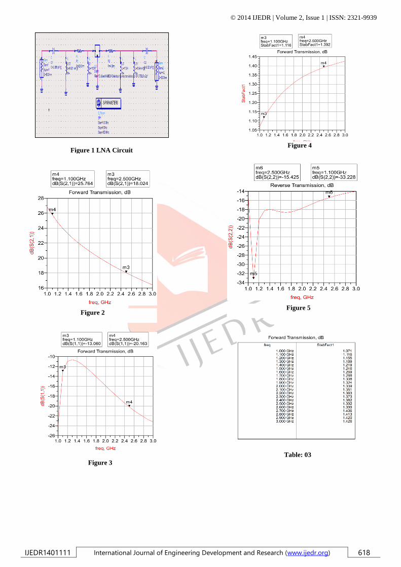
4. Simulation Circuit & Results
By using advance design system (ADS) software design a low noise amplifier circuit. The Semitic diagram is show in
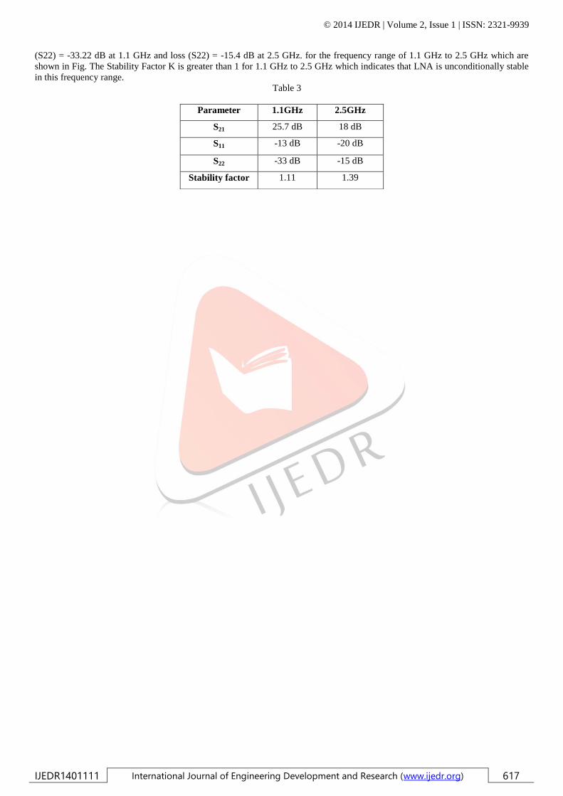
figure. Simulation results of LNA are shown in Figure. The designed low noise amplifier offers forward gain (S21) = 24.27 dB
at 1.1 GHz and (S21) = 18.06 dB. Input return loss (S11) =- 13 dB at 1.1 GHz and (S11) =- 20 dB at 2.5 GHz. Output return loss
© 2014 IJEDR | Volume 2, Issue 1 | ISSN: 2321-9939
IJEDR1401111 International Journal of Engineering Development and Research (www.ijedr.org) 617
(S22) = -33.22 dB at 1.1 GHz and loss (S22) = -15.4 dB at 2.5 GHz. for the frequency range of 1.1 GHz to 2.5 GHz which are
shown in Fig. The Stability Factor K is greater than 1 for 1.1 GHz to 2.5 GHz which indicates that LNA is unconditionally stable
in this frequency range.
Table 3
Parameter 1.1GHz 2.5GHz
S21 25.7 dB 18 dB
S11 -13 dB -20 dB
S22 -33 dB -15 dB
Stability factor 1.11 1.39
© 2014 IJEDR | Volume 2, Issue 1 | ISSN: 2321-9939
IJEDR1401111 International Journal of Engineering Development and Research (www.ijedr.org) 618
Figure 1 LNA Circuit
Figure 2
Figure 3
Figure 4
Figure 5
Table: 03
© 2014 IJEDR | Volume 2, Issue 1 | ISSN: 2321-9939
IJEDR1401111 International Journal of Engineering Development and Research (www.ijedr.org) 619
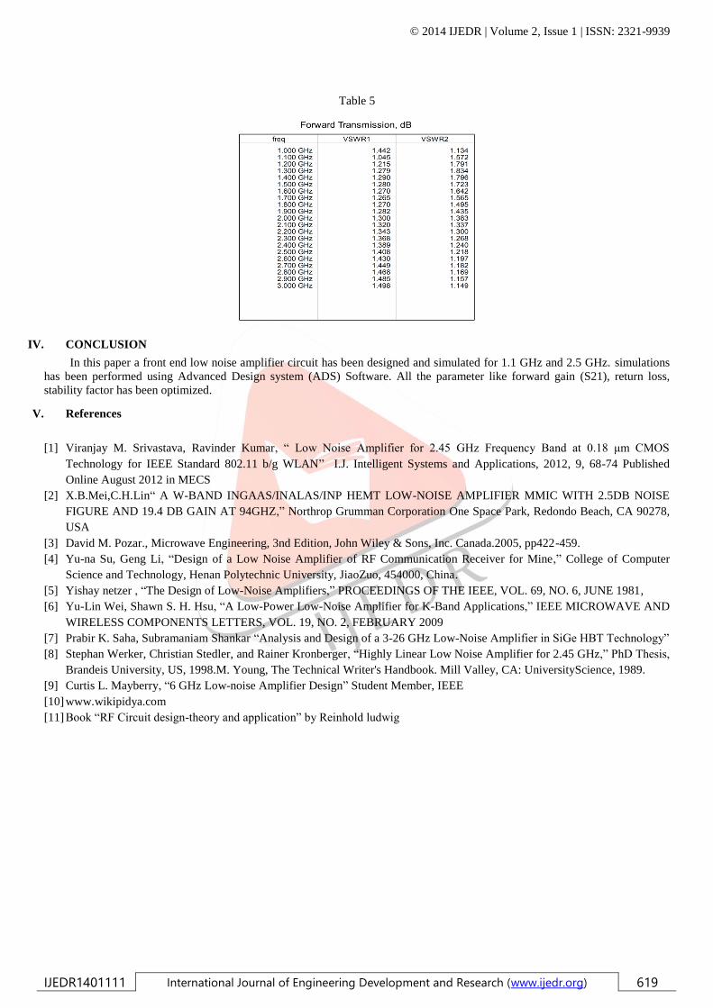
Table 5
IV. CONCLUSION
In this paper a front end low noise amplifier circuit has been designed and simulated for 1.1 GHz and 2.5 GHz. simulations
has been performed using Advanced Design system (ADS) Software. All the parameter like forward gain (S21), return loss,
stability factor has been optimized.
V. References
[1] Viranjay M. Srivastava, Ravinder Kumar, “ Low Noise Amplifier for 2.45 GHz Frequency Band at 0.18 μm CMOS
Technology for IEEE Standard 802.11 b/g WLAN” I.J. Intelligent Systems and Applications, 2012, 9, 68-74 Published
Online August 2012 in MECS
[2] X.B.Mei,C.H.Lin“ A W-BAND INGAAS/INALAS/INP HEMT LOW-NOISE AMPLIFIER MMIC WITH 2.5DB NOISE
FIGURE AND 19.4 DB GAIN AT 94GHZ,” Northrop Grumman Corporation One Space Park, Redondo Beach, CA 90278,
USA
[3] David M. Pozar., Microwave Engineering, 3nd Edition, John Wiley & Sons, Inc. Canada.2005, pp422-459.
[4] Yu-na Su, Geng Li, “Design of a Low Noise Amplifier of RF Communication Receiver for Mine,” College of Computer
Science and Technology, Henan Polytechnic University, JiaoZuo, 454000, China.
[5] Yishay netzer , “The Design of Low-Noise Amplifiers,” PROCEEDINGS OF THE IEEE, VOL. 69, NO. 6, JUNE 1981,
[6] Yu-Lin Wei, Shawn S. H. Hsu, “A Low-Power Low-Noise Amplifier for K-Band Applications,” IEEE MICROWAVE AND
WIRELESS COMPONENTS LETTERS, VOL. 19, NO. 2, FEBRUARY 2009
[7] Prabir K. Saha, Subramaniam Shankar “Analysis and Design of a 3-26 GHz Low-Noise Amplifier in SiGe HBT Technology”
[8] Stephan Werker, Christian Stedler, and Rainer Kronberger, “Highly Linear Low Noise Amplifier for 2.45 GHz,” PhD Thesis,
Brandeis University, US, 1998.M. Young, The Technical Writer's Handbook. Mill Valley, CA: UniversityScience, 1989.
[9] Curtis L. Mayberry, “6 GHz Low-noise Amplifier Design” Student Member, IEEE
[10] www.wikipidya.com
[11] Book “RF Circuit design-theory and application” by Reinhold ludwig