Embed Size (px)
DESCRIPTION
Low Power Design Methodologies and Flows. Low-Power Design Methodology - Motivations. Minimize power Reduce power in various modes of device operation Dynamic power, leakage power, or total power Minimize time Reduce power quickly Complete the design in as little time as possible - PowerPoint PPT Presentation
Citation preview

Jerry FrenkilJan Rabaey
Low Power Design Essentials ©2008 Chapter 12
Low Power Design Methodologies and Flows
Low Power Design Essentials ©2008 12.2
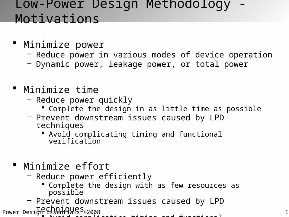
Low-Power Design Methodology - Motivations
Minimize power– Reduce power in various modes of device operation– Dynamic power, leakage power, or total power
Minimize time– Reduce power quickly
Complete the design in as little time as possible– Prevent downstream issues caused by LPD techniques
Avoid complicating timing and functional verification
Minimize effort– Reduce power efficiently
Complete the design with as few resources as possible– Prevent downstream issues caused by LPD techniques
Avoid complicating timing and functional verification
Low Power Design Essentials ©2008 12.3
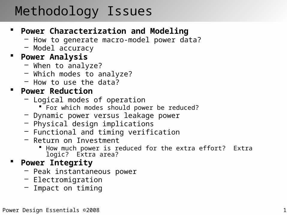
Methodology Issues Power Characterization and Modeling
– How to generate macro-model power data?– Model accuracy
Power Analysis– When to analyze?– Which modes to analyze?– How to use the data?
Power Reduction– Logical modes of operation
For which modes should power be reduced?– Dynamic power versus leakage power– Physical design implications– Functional and timing verification– Return on Investment
How much power is reduced for the extra effort? Extra logic? Extra area? Power Integrity
– Peak instantaneous power– Electromigration– Impact on timing
Low Power Design Essentials ©2008 12.4
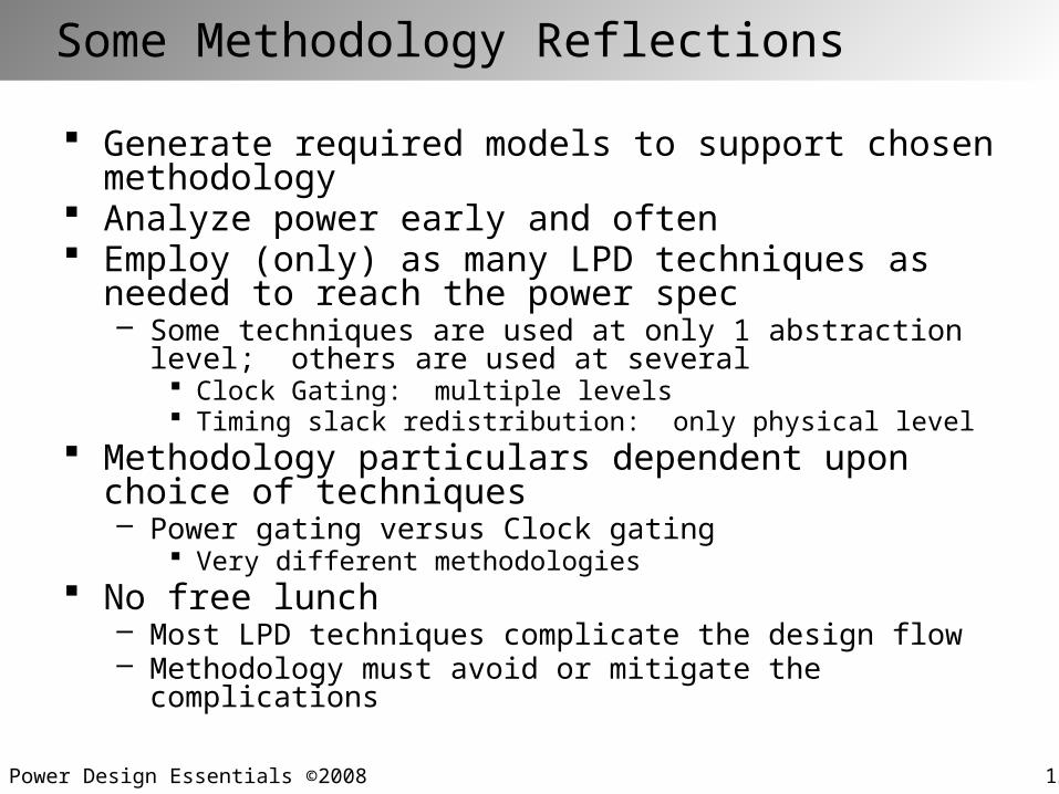
Some Methodology Reflections
Generate required models to support chosen methodology Analyze power early and often Employ (only) as many LPD techniques as needed to
reach the power spec– Some techniques are used at only 1 abstraction level; others are
used at several Clock Gating: multiple levels Timing slack redistribution: only physical level
Methodology particulars dependent upon choice of techniques– Power gating versus Clock gating
Very different methodologies No free lunch
– Most LPD techniques complicate the design flow– Methodology must avoid or mitigate the complications
Low Power Design Essentials ©2008 12.5
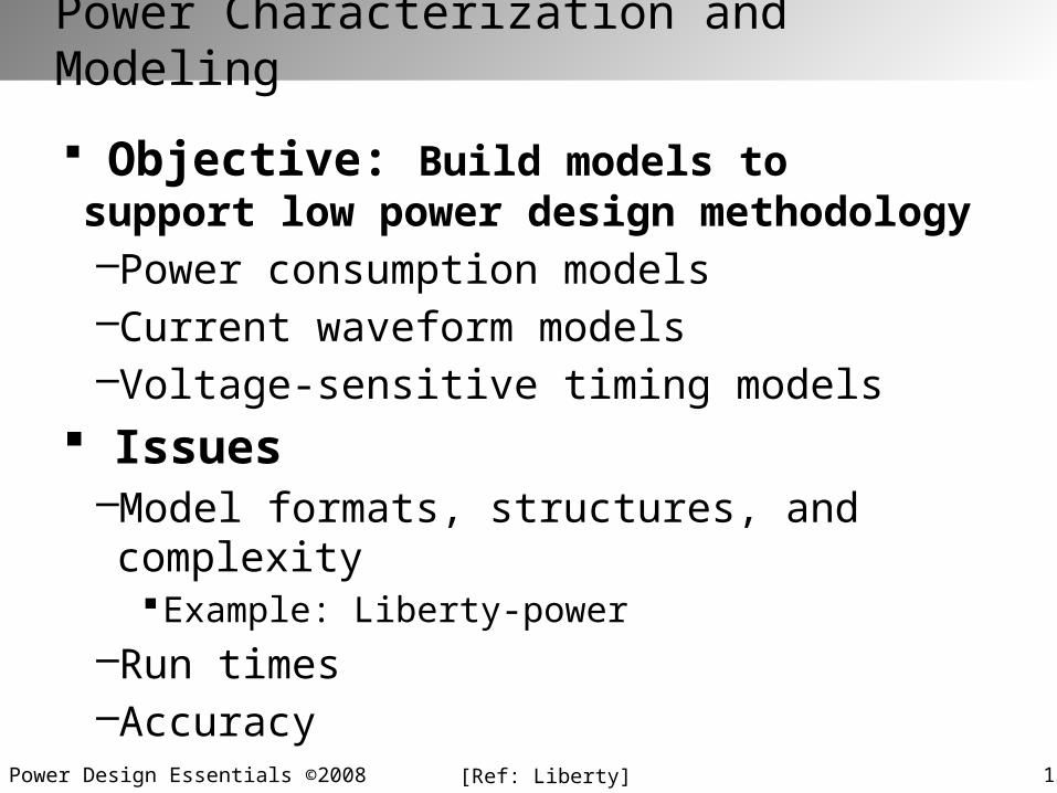
Power Characterization and Modeling
Objective: Build models to support low power design methodology–Power consumption models–Current waveform models–Voltage-sensitive timing models
Issues–Model formats, structures, and complexity
Example: Liberty-power–Run times–Accuracy
[Ref: Liberty]
Low Power Design Essentials ©2008 12.6
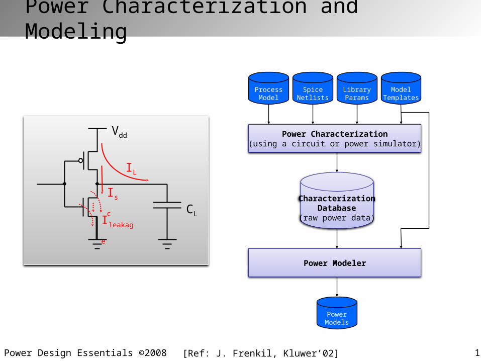
Power Characterization and Modeling
ProcessModel
LibraryParams
SpiceNetlists
ModelTemplates
Power Characterization(using a circuit or power simulator)
CharacterizationDatabase
(raw power data)
Power Modeler
PowerModels
IL
Isc
Vdd
CLIleakage
[Ref: J. Frenkil, Kluwer’02]
Low Power Design Essentials ©2008 12.7
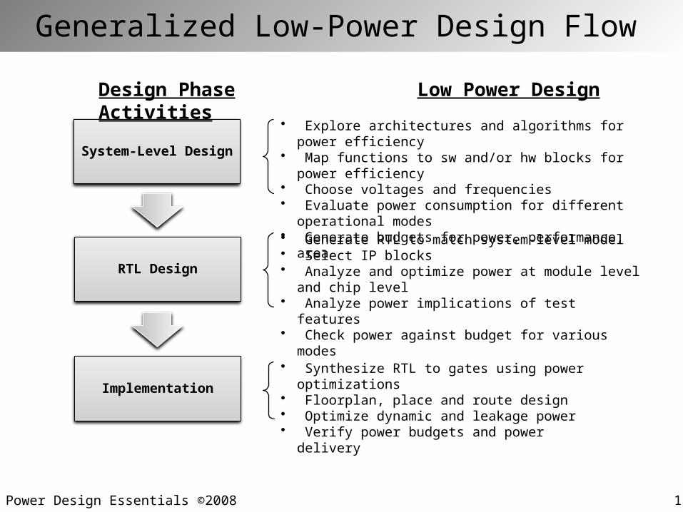
Generalized Low-Power Design Flow
System-Level Design
RTL Design
Implementation
• Explore architectures and algorithms for power efficiency• Map functions to sw and/or hw blocks for power efficiency• Choose voltages and frequencies • Evaluate power consumption for different operational
modes• Generate budgets for power, performance, area
• Generate RTL to match system-level model• Select IP blocks• Analyze and optimize power at module level and chip
level • Analyze power implications of test features• Check power against budget for various modes
• Synthesize RTL to gates using power optimizations• Floorplan, place and route design• Optimize dynamic and leakage power• Verify power budgets and power delivery
Design Phase Low Power Design Activities
Low Power Design Essentials ©2008 12.8
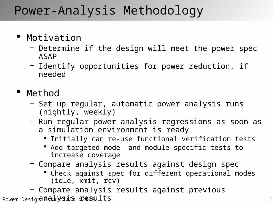
Power-Analysis Methodology
Motivation– Determine if the design will meet the power spec ASAP– Identify opportunities for power reduction, if needed
Method– Set up regular, automatic power analysis runs (nightly, weekly)– Run regular power analysis regressions as soon as a simulation
environment is ready Initially can re-use functional verification tests Add targeted mode- and module-specific tests to increase coverage
– Compare analysis results against design spec Check against spec for different operational modes (idle, xmit, rcv)
– Compare analysis results against previous analysis results Identify power mistakes - changes / fixes resulting in increased power
– Identify opportunities for power reduction
Low Power Design Essentials ©2008 12.9
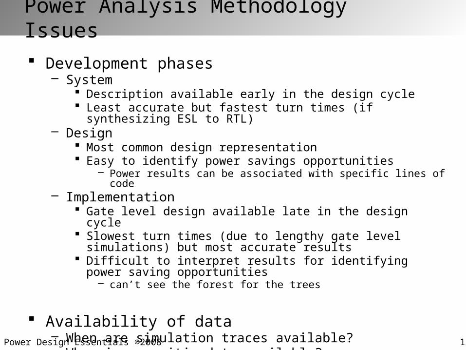
Power Analysis Methodology Issues
Development phases– System
Description available early in the design cycle Least accurate but fastest turn times (if synthesizing ESL to RTL)
– Design Most common design representation Easy to identify power savings opportunities
– Power results can be associated with specific lines of code– Implementation
Gate level design available late in the design cycle Slowest turn times (due to lengthy gate level simulations) but most
accurate results Difficult to interpret results for identifying power saving opportunities
– can’t see the forest for the trees
Availability of data– When are simulation traces available?– When is parasitic data available?
Low Power Design Essentials ©2008 12.10
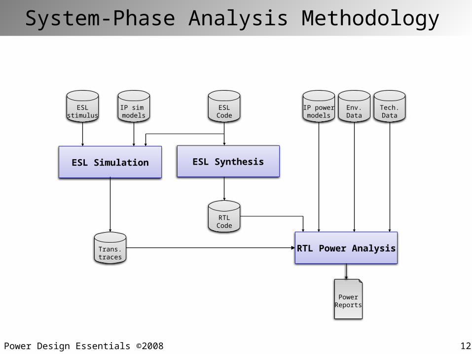
System-Phase Analysis Methodology
ESL Simulation
PowerReports
ESL Synthesis
RTL Power Analysis
Tech.Data
Env.Data
ESLCode
IP sim models
ESLstimulus
RTLCode
Trans.traces
IP powermodels
Low Power Design Essentials ©2008 12.11
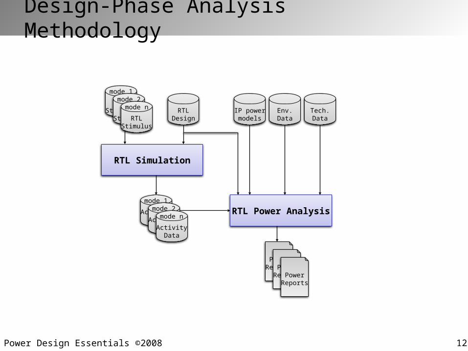
Design-Phase Analysis Methodology
ActivityData
RTLDesign
Tech.Data
Env.Data
PowerReports
RTL Simulation
RTLStimulus
RTL Power AnalysisActivityDataActivity
Data
RTLStimulusRTL
Stimulus
PowerReportsPower
Reports
mode 1mode 2
mode n
mode 1mode 2
mode n
IP powermodels
Low Power Design Essentials ©2008 12.12
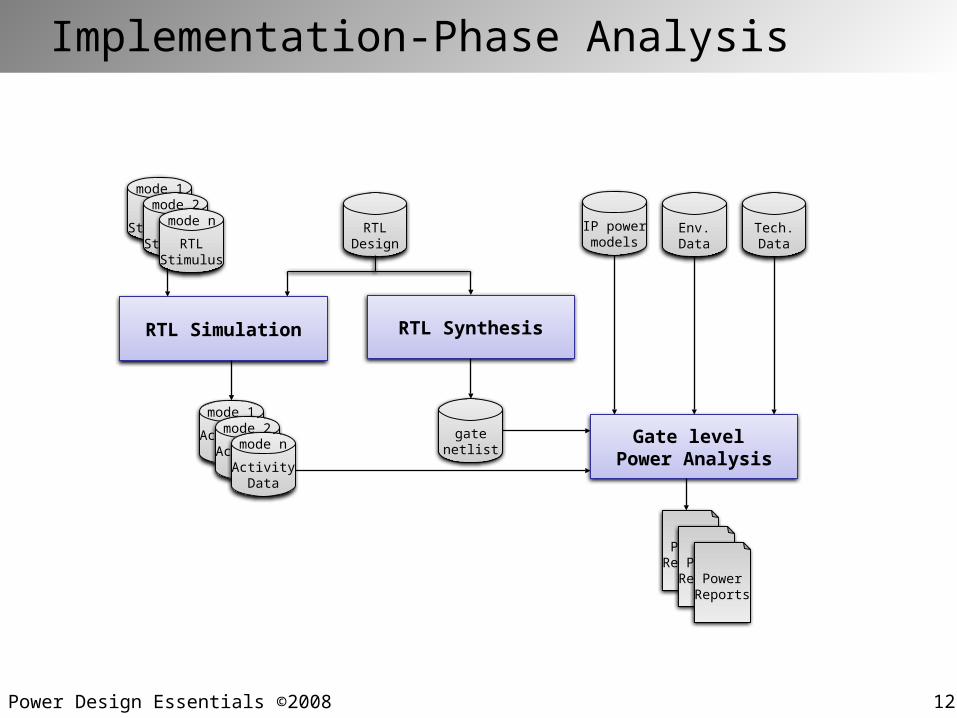
Implementation-Phase Analysis
ActivityData
RTLDesign
Tech.Data
Env.Data
PowerReports
RTL Simulation
RTLStimulus
Gate level Power AnalysisActivity
DataActivityData
RTLStimulusRTL
Stimulus
PowerReportsPower
Reports
mode 1mode 2
mode n
mode 1mode 2
mode n
RTL Synthesis
gatenetlist
IP powermodels
Low Power Design Essentials ©2008 12.13
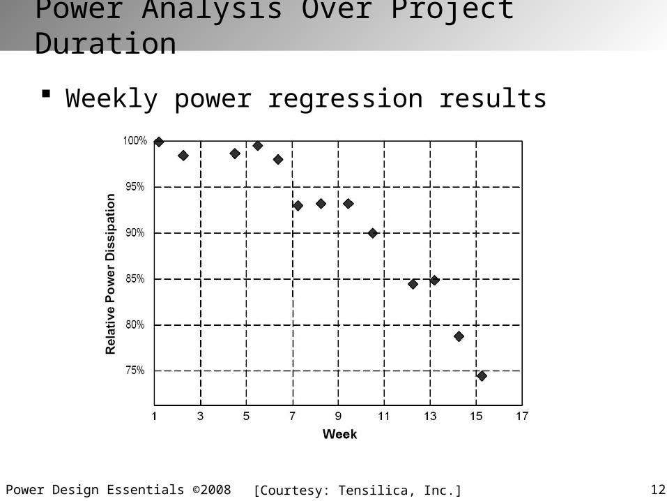
Power Analysis Over Project Duration
Weekly power regression results
[Courtesy: Tensilica, Inc.]
Low Power Design Essentials ©2008 12.14
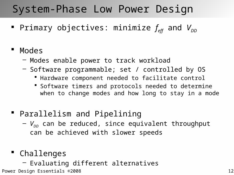
System-Phase Low Power Design
Primary objectives: minimize feff and VDD
Modes– Modes enable power to track workload– Software programmable; set / controlled by OS
Hardware component needed to facilitate control Software timers and protocols needed to determine when to change
modes and how long to stay in a mode
Parallelism and Pipelining– VDD can be reduced, since equivalent throughput can be achieved
with slower speeds
Challenges– Evaluating different alternatives
Low Power Design Essentials ©2008 12.15
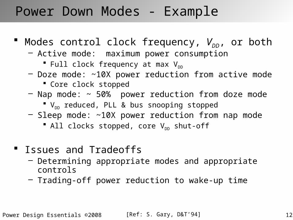
Power Down Modes - Example
Modes control clock frequency, VDD, or both– Active mode: maximum power consumption
Full clock frequency at max VDD
– Doze mode: ~10X power reduction from active mode Core clock stopped
– Nap mode: ~ 50% power reduction from doze mode VDD reduced, PLL & bus snooping stopped
– Sleep mode: ~10X power reduction from nap mode All clocks stopped, core VDD shut-off
Issues and Tradeoffs– Determining appropriate modes and appropriate controls– Trading-off power reduction to wake-up time
[Ref: S. Gary, D&T’94]
Low Power Design Essentials ©2008 12.16
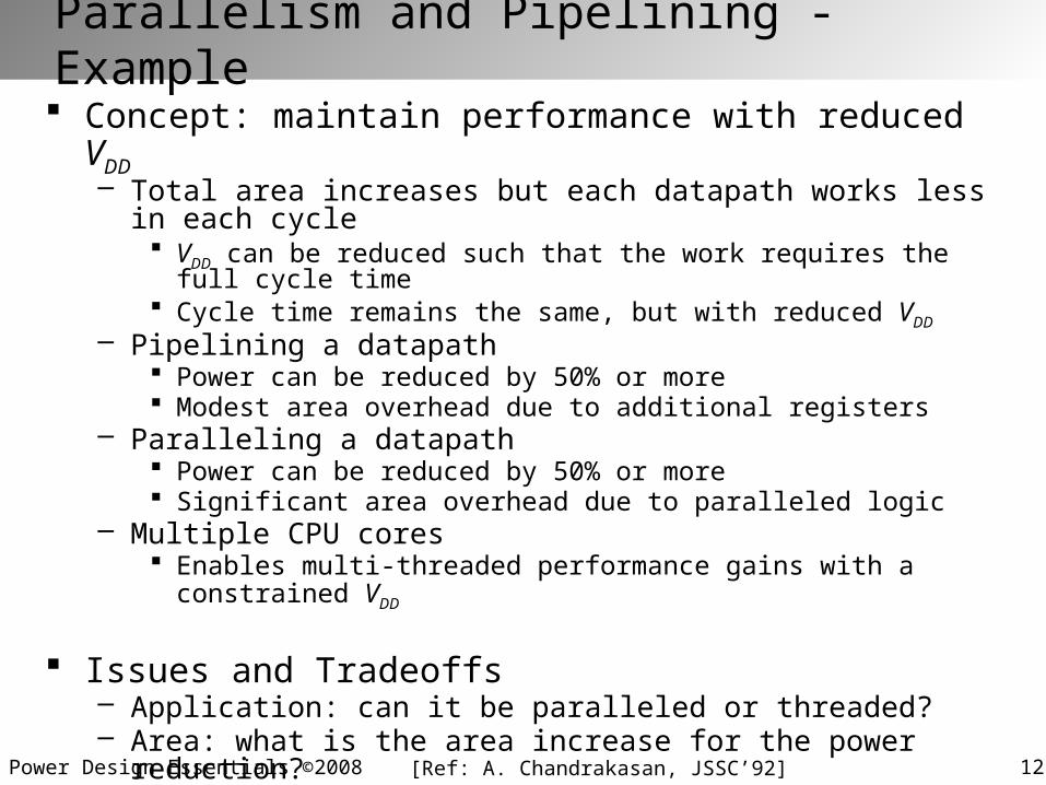
Parallelism and Pipelining - Example Concept: maintain performance with reduced VDD
– Total area increases but each datapath works less in each cycle VDD can be reduced such that the work requires the full cycle time Cycle time remains the same, but with reduced VDD
– Pipelining a datapath Power can be reduced by 50% or more Modest area overhead due to additional registers
– Paralleling a datapath Power can be reduced by 50% or more Significant area overhead due to paralleled logic
– Multiple CPU cores Enables multi-threaded performance gains with a constrained VDD
Issues and Tradeoffs– Application: can it be paralleled or threaded?– Area: what is the area increase for the power reduction?– Latency: how much can be tolerated?
[Ref: A. Chandrakasan, JSSC’92]
Low Power Design Essentials ©2008 12.17
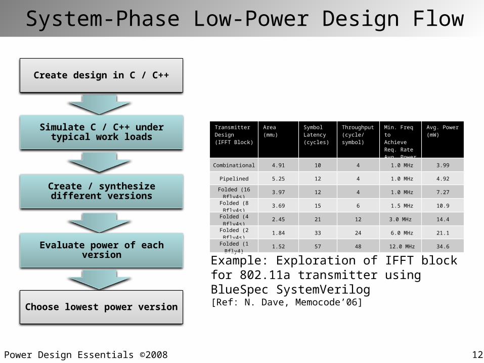
System-Phase Low-Power Design Flow
Create design in C / C++
Create / synthesize different versions
Evaluate power of each version
Choose lowest power version
Simulate C / C++ under typical work loads
Example: Exploration of IFFT block for 802.11a transmitter using BlueSpec SystemVerilog[Ref: N. Dave, Memocode’06]
Transmitter Design(IFFT Block)
Area(mm2)
SymbolLatency(cycles)
Throughput(cycle/symbol)
Min. Freq toAchieve Req. RateAvg. Power
Avg. Power(mW)
Combinational 4.91 10 4 1.0 MHz 3.99
Pipelined 5.25 12 4 1.0 MHz 4.92
Folded (16 Bfly4s) 3.97 12 4 1.0 MHz 7.27
Folded (8 Bfly4s) 3.69 15 6 1.5 MHz 10.9
Folded (4 Bfly4s) 2.45 21 12 3.0 MHz 14.4
Folded (2 Bfly4s) 1.84 33 24 6.0 MHz 21.1
Folded (1 Bfly4) 1.52 57 48 12.0 MHz 34.6
Low Power Design Essentials ©2008 12.18
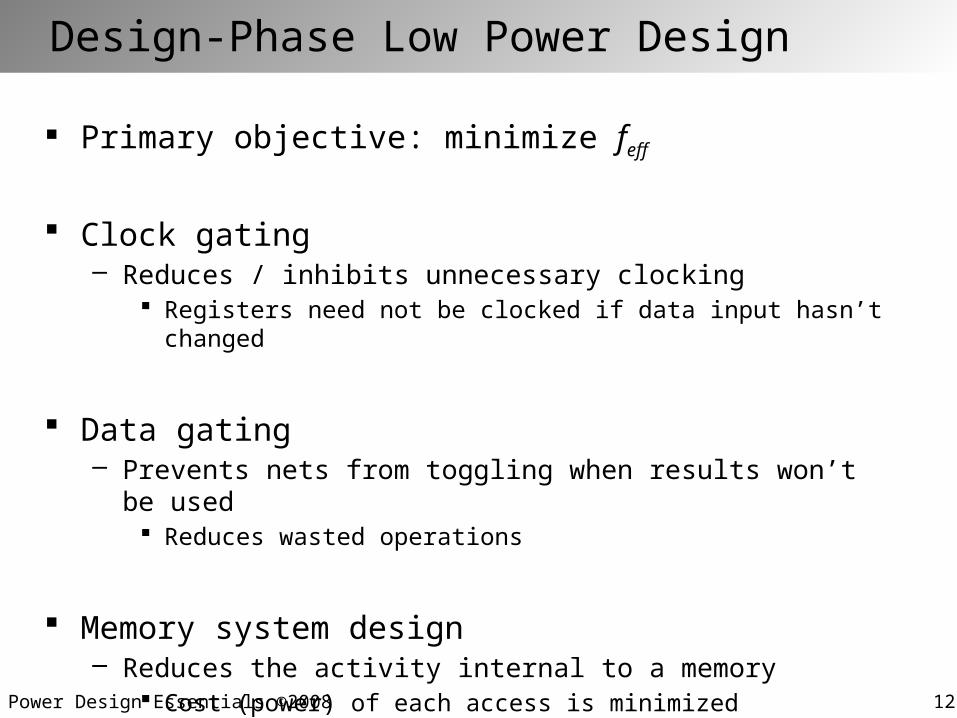
Design-Phase Low Power Design
Primary objective: minimize feff
Clock gating– Reduces / inhibits unnecessary clocking
Registers need not be clocked if data input hasn’t changed
Data gating– Prevents nets from toggling when results won’t be used
Reduces wasted operations
Memory system design– Reduces the activity internal to a memory
Cost (power) of each access is minimized
Low Power Design Essentials ©2008 12.19
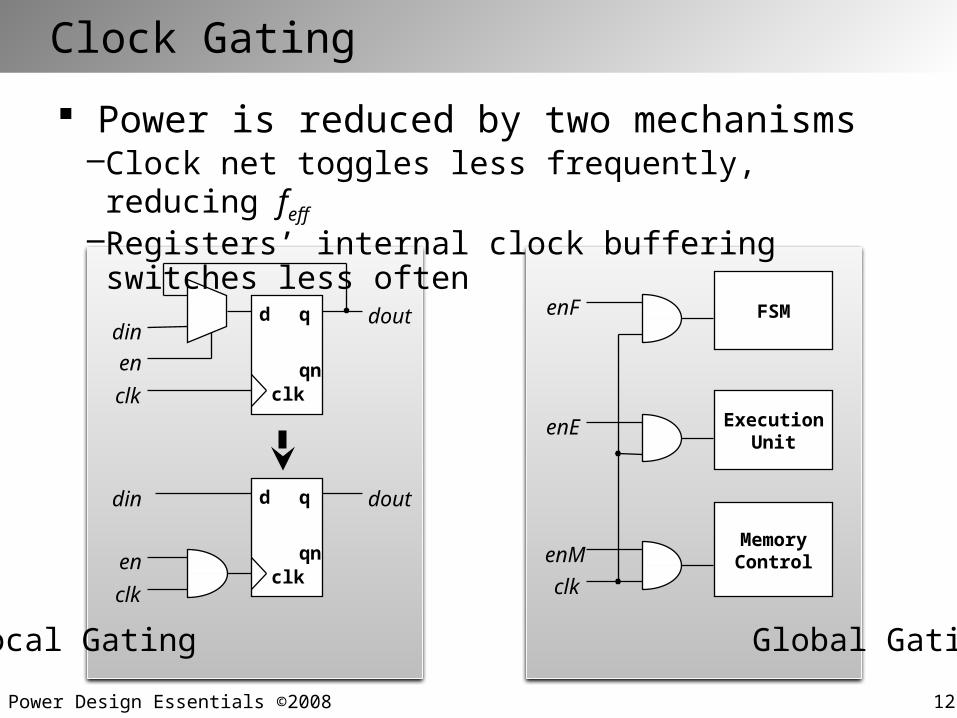
Clock Gating
Local Gating Global Gating
clkqn
qd doutdinenclk
clkqn
qd doutdin
enclk
FSM
ExecutionUnit
MemoryControl
clkenM
enE
enF
Power is reduced by two mechanisms–Clock net toggles less frequently, reducing feff–Registers’ internal clock buffering switches less often
Low Power Design Essentials ©2008 12.20
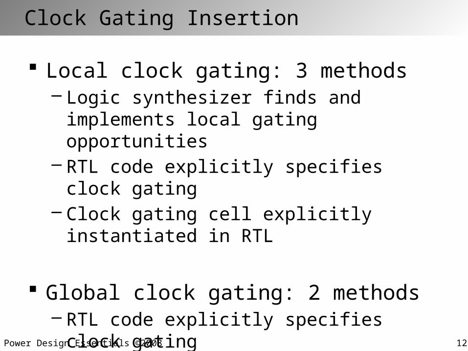
Clock Gating Insertion
Local clock gating: 3 methods– Logic synthesizer finds and implements local
gating opportunities– RTL code explicitly specifies clock gating– Clock gating cell explicitly instantiated in RTL
Global clock gating: 2 methods– RTL code explicitly specifies clock gating– Clock gating cell explicitly instantiated in RTL
Low Power Design Essentials ©2008 12.21
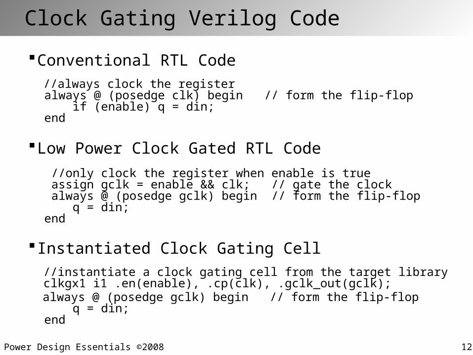
Clock Gating Verilog Code
Conventional RTL Code //always clock the register always @ (posedge clk) begin // form the flip-flop if (enable) q = din; end
Low Power Clock Gated RTL Code //only clock the register when enable is true assign gclk = enable && clk; // gate the clock always @ (posedge gclk) begin // form the flip-flop q = din; end
Instantiated Clock Gating Cell //instantiate a clock gating cell from the target library clkgx1 i1 .en(enable), .cp(clk), .gclk_out(gclk);
always @ (posedge gclk) begin // form the flip-flop q = din; end
Low Power Design Essentials ©2008 12.22
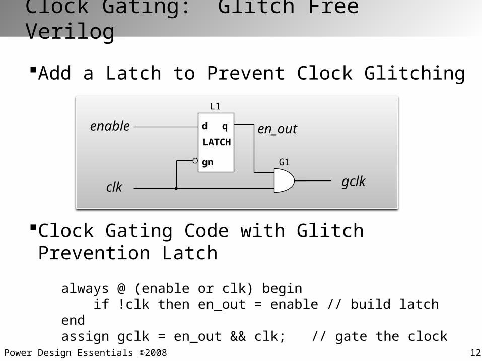
Clock Gating: Glitch Free Verilog
Add a Latch to Prevent Clock Glitching
Clock Gating Code with Glitch Prevention Latch
always @ (enable or clk) begin if !clk then en_out = enable // build latch end assign gclk = en_out && clk; // gate the clock
en_out
gclkclk
L1
gn
qdLATCH
G1
enable
Low Power Design Essentials ©2008 12.23
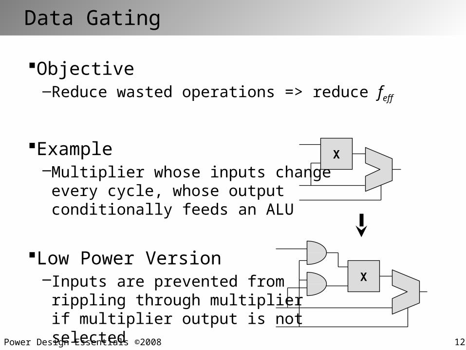
Data Gating
Objective–Reduce wasted operations => reduce feff
Example–Multiplier whose inputs change
every cycle, whose output conditionally feeds an ALU
Low Power Version–Inputs are prevented from
rippling through multiplierif multiplier output is not selected
X
X
Low Power Design Essentials ©2008 12.24
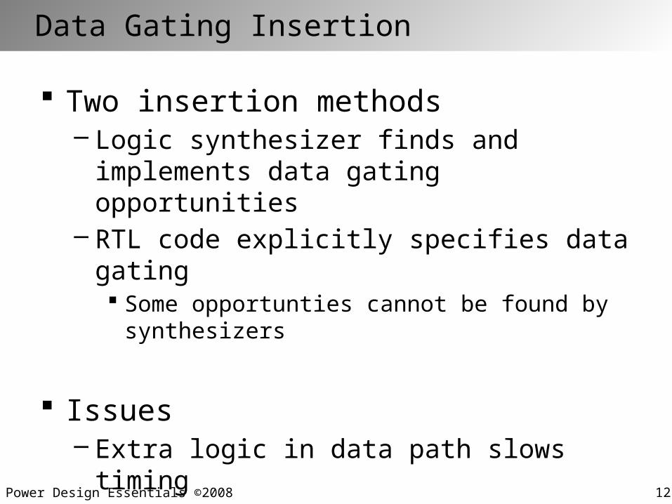
Data Gating Insertion
Two insertion methods– Logic synthesizer finds and implements data
gating opportunities– RTL code explicitly specifies data gating
Some opportunties cannot be found by synthesizers
Issues– Extra logic in data path slows timing– Additional area due to gating cells
Low Power Design Essentials ©2008 12.25
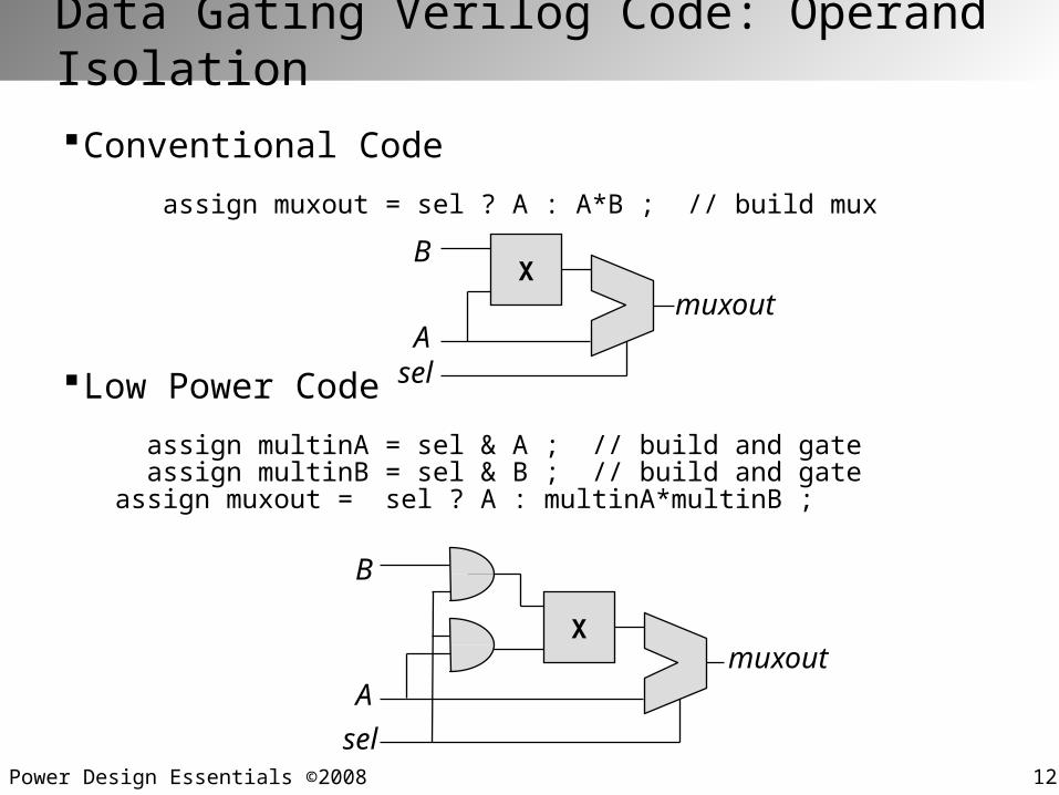
Data Gating Verilog Code: Operand Isolation
Conventional Code assign muxout = sel ? A : A*B ; // build mux
Low Power Code assign multinA = sel & A ; // build and gate assign multinB = sel & B ; // build and gate assign muxout = sel ? A : multinA*multinB ;
X
sel
B
Amuxout
X
sel
B
Amuxout
Low Power Design Essentials ©2008 12.26
Memory System Design
Primary objectives: minimize feff and Ceff
– Reduce number of accesses or (power) cost of an access
Power Reduction Methods– Memory banking / splitting– Minimization of number of memory accesses
Challenges and Tradeoffs– Dependency upon access patterns– Placement and routing
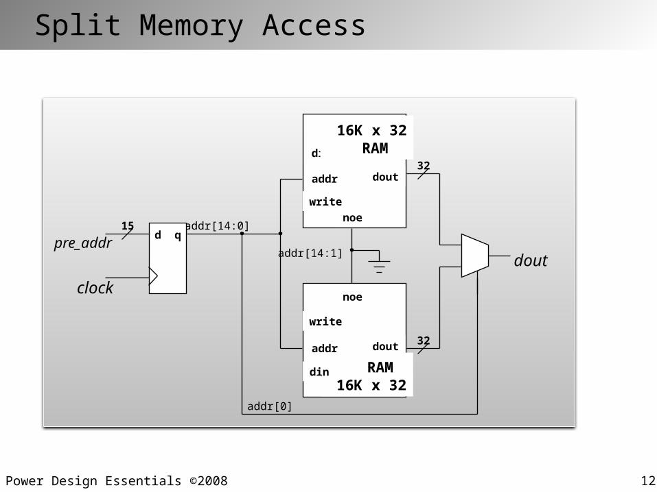
Low Power Design Essentials ©2008 12.27
Split Memory Access
dout
addr[0]
32
32
addr[14:1]
addr[14:0]
clock
pre_addr qd15
write
dout
RAM 16K x 32
noe
din
addr
addr
din
dout
16K x 32 RAM
noewrite
Low Power Design Essentials ©2008 12.28
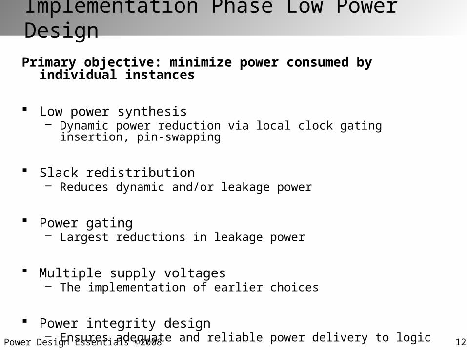
Implementation Phase Low Power Design
Primary objective: minimize power consumed by individual instances
Low power synthesis– Dynamic power reduction via local clock gating insertion, pin-swapping
Slack redistribution– Reduces dynamic and/or leakage power
Power gating– Largest reductions in leakage power
Multiple supply voltages– The implementation of earlier choices
Power integrity design– Ensures adequate and reliable power delivery to logic
Low Power Design Essentials ©2008 12.29
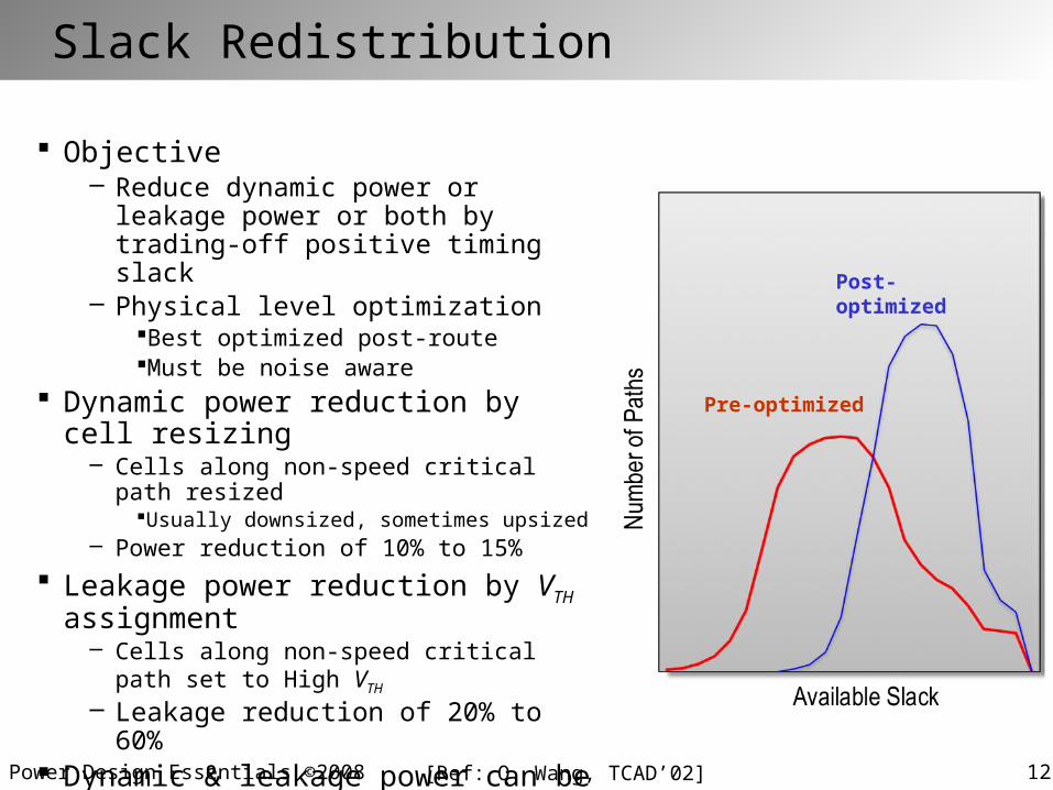
Slack Redistribution
Objective– Reduce dynamic power or leakage power
or both by trading-off positive timing slack – Physical level optimization
Best optimized post-routeMust be noise aware
Dynamic power reduction by cell resizing– Cells along non-speed critical path resized
Usually downsized, sometimes upsized– Power reduction of 10% to 15%
Leakage power reduction by VTH assignment
– Cells along non-speed critical path set to High VTH
– Leakage reduction of 20% to 60% Dynamic & leakage power can be
optimized independently or together
Pre-optimized
Post-optimized
[Ref: Q. Wang, TCAD’02]
Low Power Design Essentials ©2008 12.30
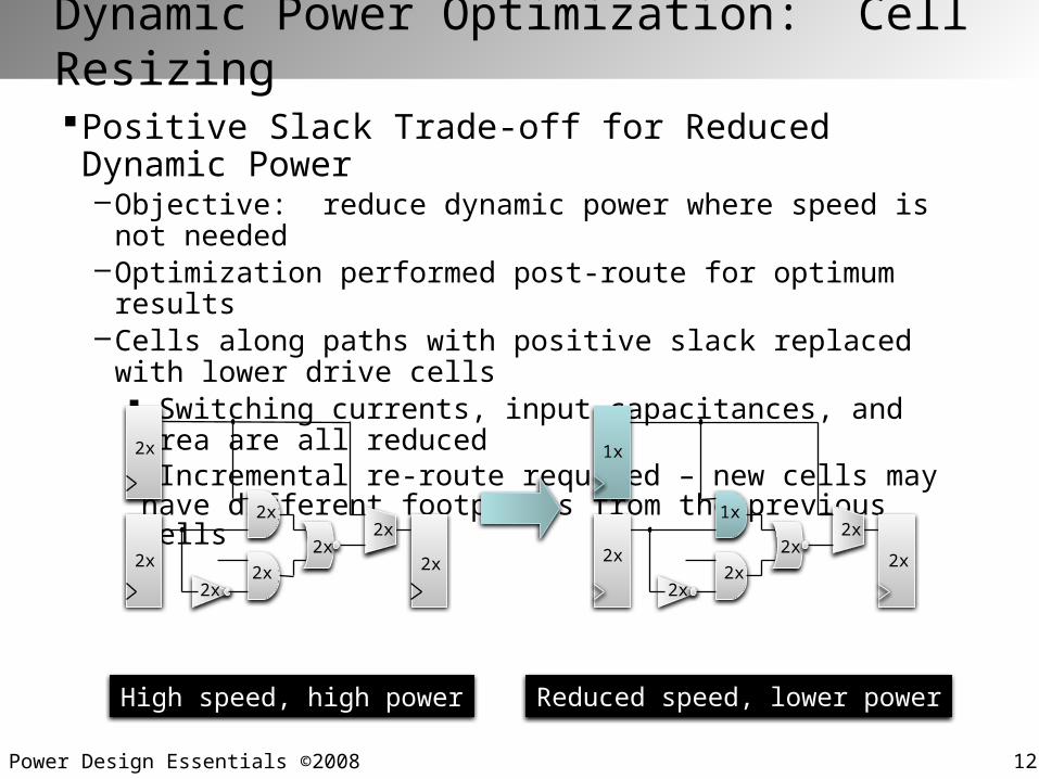
Dynamic Power Optimization: Cell Resizing
Positive Slack Trade-off for Reduced Dynamic Power–Objective: reduce dynamic power where speed is not needed–Optimization performed post-route for optimum results–Cells along paths with positive slack replaced with lower drive cells
Switching currents, input capacitances, and area are all reduced Incremental re-route required – new cells may have different footprints from the previous cells
High speed, high power Reduced speed, lower power
2x2x
2x
2x
2x
2x
2x2x
1x
2x
2x2x
2x2x
2x
1x
Low Power Design Essentials ©2008 12.31
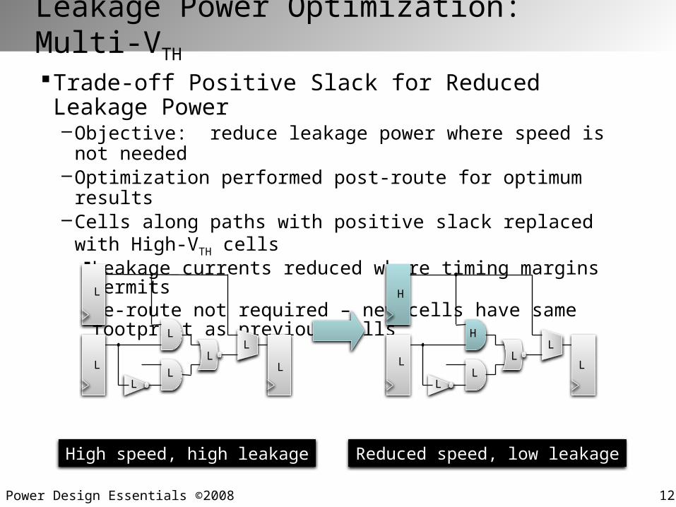
Leakage Power Optimization: Multi-VTH
Trade-off Positive Slack for Reduced Leakage Power–Objective: reduce leakage power where speed is not needed–Optimization performed post-route for optimum results–Cells along paths with positive slack replaced with High-VTH cells
Leakage currents reduced where timing margins permitsRe-route not required – new cells have same footprint as previous cells
LL
L
L
L
L
LL
H
L
LL
LL
L
H
High speed, high leakage Reduced speed, low leakage
Low Power Design Essentials ©2008 12.32
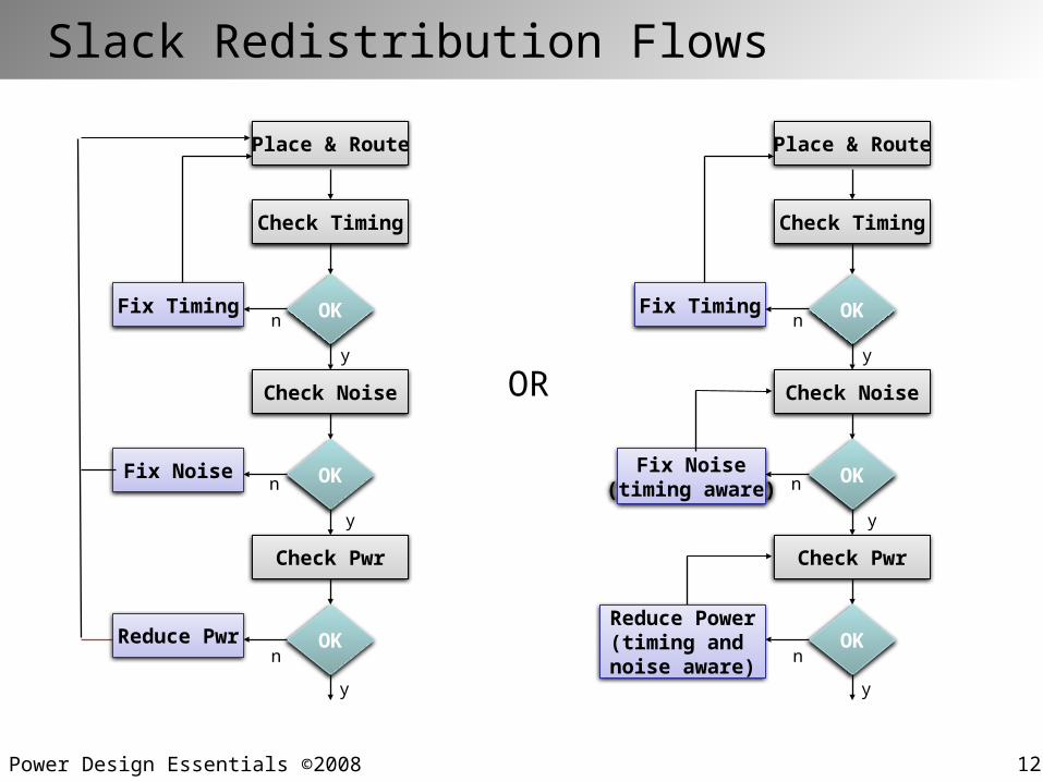
Slack Redistribution Flows
OK
Check Timing
Fix Timing
Fix Noise
Check Noise
OK
OK
Check Pwr
y
n
y
nReduce Pwr
n
y
Place & Route
OK
Check Timing
Fix Timing
Fix Noise(timing aware)
Check Noise
OK
OK
Check Pwr
y
n
y
n
n
y
Place & Route
OR
Reduce Power(timing and noise aware)
Low Power Design Essentials ©2008 12.33
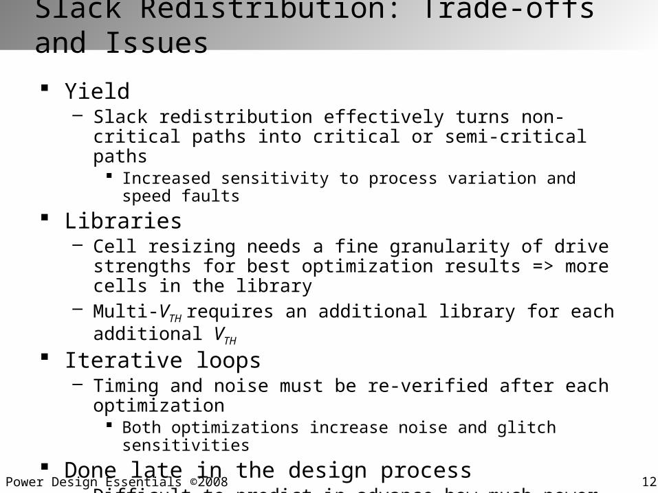
Slack Redistribution: Trade-offs and Issues
Yield– Slack redistribution effectively turns non-critical paths into critical
or semi-critical paths Increased sensitivity to process variation and speed faults
Libraries– Cell resizing needs a fine granularity of drive strengths for best
optimization results => more cells in the library– Multi-VTH requires an additional library for each additional VTH
Iterative loops– Timing and noise must be re-verified after each optimization
Both optimizations increase noise and glitch sensitivities Done late in the design process
– Difficult to predict in advance how much power will be saved Very dependent upon design characteristics
Low Power Design Essentials ©2008 12.34
Power Gating
Objective– Reduce leakage currents by inserting a switch transistor (usually
high VTH) into the logic stack (usually low VTH) Switch transistors change the bias points (VSB) of the logic transistors
Most effective for systems with standby operational modes– 1 to 3 orders of magnitude leakage reduction possible– But switches add many complications
Virtual Ground
sleep
Vdd
LogicCell
SwitchCell
Vdd
LogicCell
Low Power Design Essentials ©2008 12.35
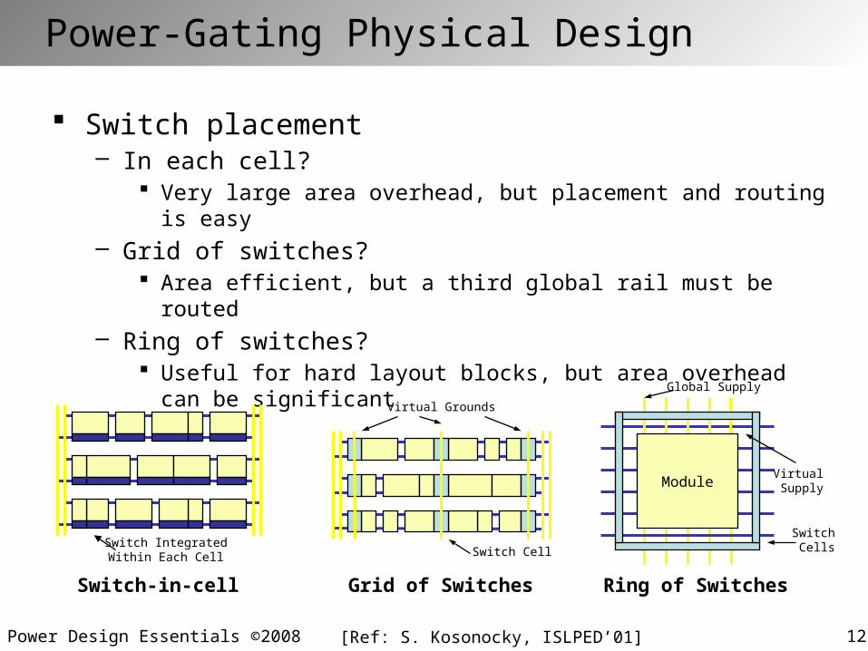
Power-Gating Physical Design
Switch placement– In each cell?
Very large area overhead, but placement and routing is easy– Grid of switches?
Area efficient, but a third global rail must be routed– Ring of switches?
Useful for hard layout blocks, but area overhead can be significant
Switch-in-cell Grid of Switches Ring of Switches
Switch IntegratedWithin Each Cell
Virtual Grounds
Switch Cell
Module
Global Supply
Virtual Supply
Switch Cells
[Ref: S. Kosonocky, ISLPED’01]
Low Power Design Essentials ©2008 12.36
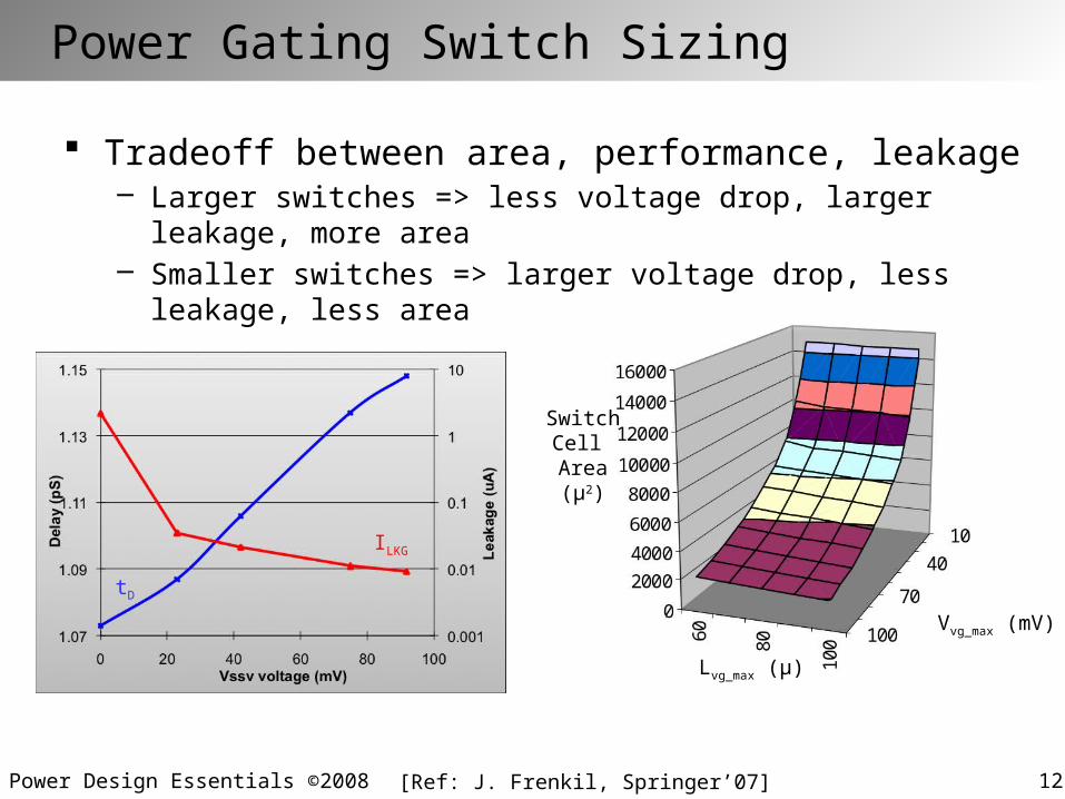
Power Gating Switch Sizing
Vvg_max (mV)
Lvg_max (µ)
SwitchCell Area(µ2)
Tradeoff between area, performance, leakage– Larger switches => less voltage drop, larger leakage, more area– Smaller switches => larger voltage drop, less leakage, less area
ILKG
tD
[Ref: J. Frenkil, Springer’07]
Low Power Design Essentials ©2008 12.37
Power Gating: Additional Issues Library design: special cells are needed
– Switches, isolation cells, state retention flip-flops (SRFFs) Headers or Footers?
– Headers better for gate leakage reduction, but ~ 2X larger Which modules, and how many, to power gate?
– Sleep control signal must be available, or must be created State retention: which registers must retain state?
– Large area overhead for using SRFFs Floating signal prevention
– Power-gate outputs that drive always-on blocks must not float Rush currents and wakeup time
– Rush currents must settle quickly and not disrupt circuit operation Delay effects and timing verification
– Switches affect source voltages which affect delays Power-up & power-down sequencing
– Controller must be designed and sequencing verified
Low Power Design Essentials ©2008 12.38
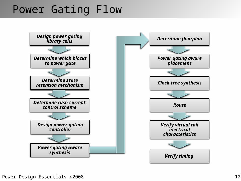
Power Gating Flow
Route
Clock tree synthesis
Verify virtual rail electrical
characteristics
Verify timing
Determine state retention mechanism
Determine which blocks to power gate
Determine rush current control scheme
Design power gating controller
Power gating aware synthesis
Determine floorplan
Power gating aware placement
Design power gating library cells
Low Power Design Essentials ©2008 12.39
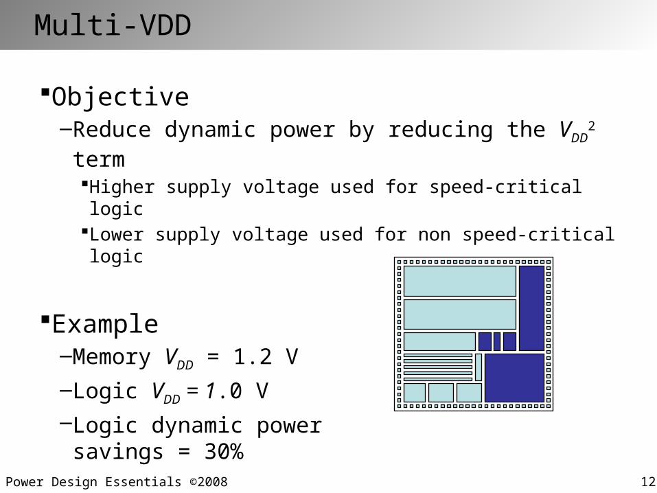
Multi-VDD
Objective–Reduce dynamic power by reducing the VDD
2 termHigher supply voltage used for speed-critical logicLower supply voltage used for non speed-critical logic
Example–Memory VDD = 1.2 V–Logic VDD = 1.0 V–Logic dynamic power
savings = 30%
Low Power Design Essentials ©2008 12.40
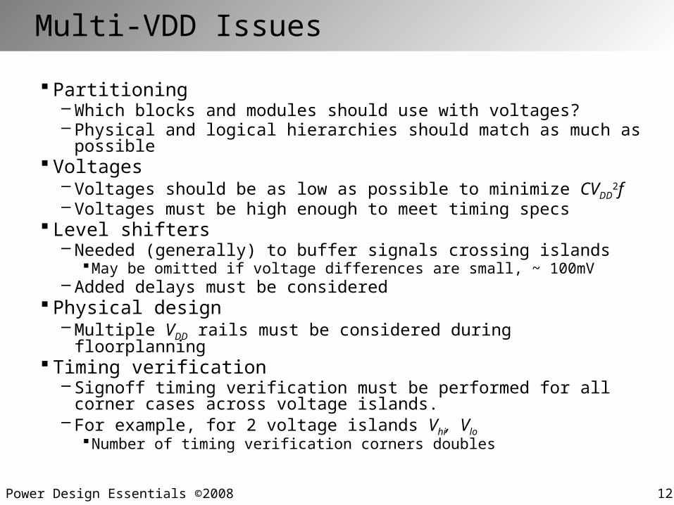
Multi-VDD Issues
Partitioning– Which blocks and modules should use with voltages?– Physical and logical hierarchies should match as much as possible
Voltages– Voltages should be as low as possible to minimize CVDD
2f– Voltages must be high enough to meet timing specs
Level shifters– Needed (generally) to buffer signals crossing islands
May be omitted if voltage differences are small, ~ 100mV– Added delays must be considered
Physical design– Multiple VDD rails must be considered during floorplanning
Timing verification– Signoff timing verification must be performed for all corner cases across
voltage islands.– For example, for 2 voltage islands Vhi, Vlo
Number of timing verification corners doubles
Low Power Design Essentials ©2008 12.41
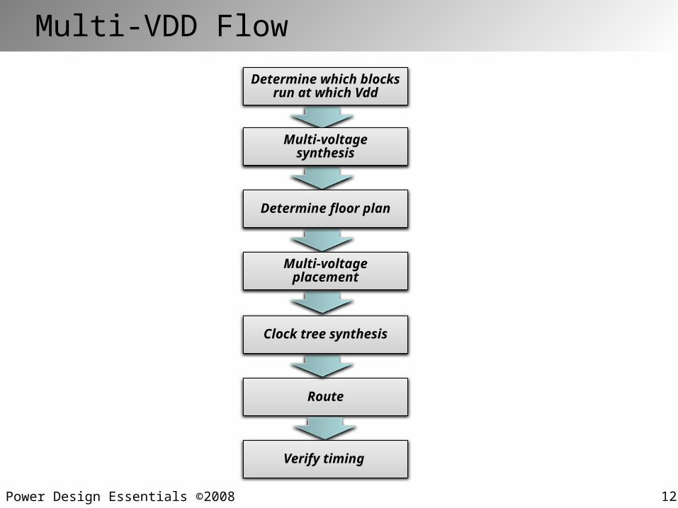
Multi-VDD Flow
Route
Determine which blocks run at which Vdd
Multi-voltage placement
Multi-voltagesynthesis
Determine floor plan
Verify timing
Clock tree synthesis
Low Power Design Essentials ©2008 12.42
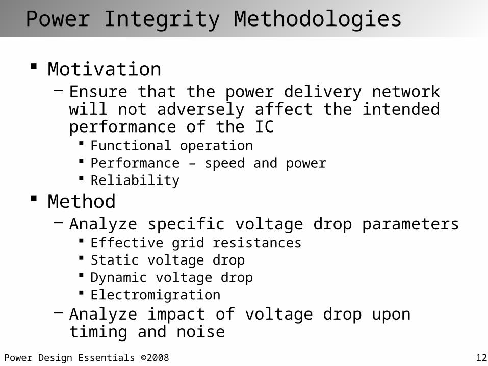
Power Integrity Methodologies
Motivation– Ensure that the power delivery network will not
adversely affect the intended performance of the IC Functional operation Performance – speed and power Reliability
Method– Analyze specific voltage drop parameters
Effective grid resistances Static voltage drop Dynamic voltage drop Electromigration
– Analyze impact of voltage drop upon timing and noise
Low Power Design Essentials ©2008 12.43
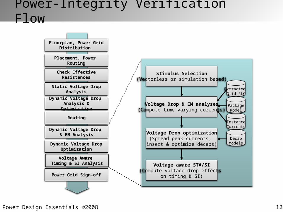
Power-Integrity Verification Flow
Placement, Power Routing
Check Effective Resistances
Static Voltage DropAnalysis
Dynamic Voltage Drop Analysis & Optimization
Routing
Dynamic Voltage Drop & EM Analysis
Power Grid Sign-off
Floorplan, Power Grid Distribution
Dynamic Voltage DropOptimization
Voltage Aware Timing & SI Analysis
Voltage Drop & EM analyses(Compute time varying currents)
Voltage Drop optimization(Spread peak currents,
insert & optimize decaps)
Voltage aware STA/SI(Compute voltage drop effects
on timing & SI)
Extracted Grid RLC
InstanceCurrents
PackageModel
Stimulus Selection(Vectorless or simulation based)
DecapModels
Low Power Design Essentials ©2008 12.44
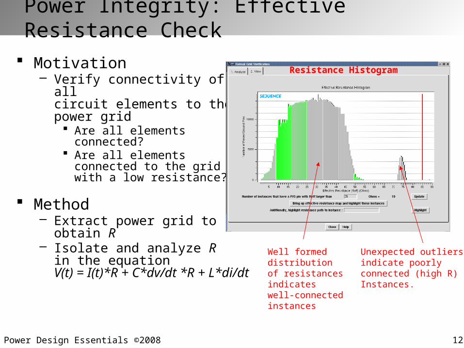
Power Integrity: Effective Resistance Check
Motivation– Verify connectivity of all
circuit elements to the power grid
Are all elements connected?
Are all elements connected to the grid with a low resistance?
Method– Extract power grid to
obtain R– Isolate and analyze R
in the equation V(t) = I(t)*R + C*dv/dt *R + L*di/dt
Well formed distribution of resistances indicateswell-connected instances
Unexpected outliers indicate poorly connected (high R)Instances.
Resistance Histogram
Low Power Design Essentials ©2008 12.45
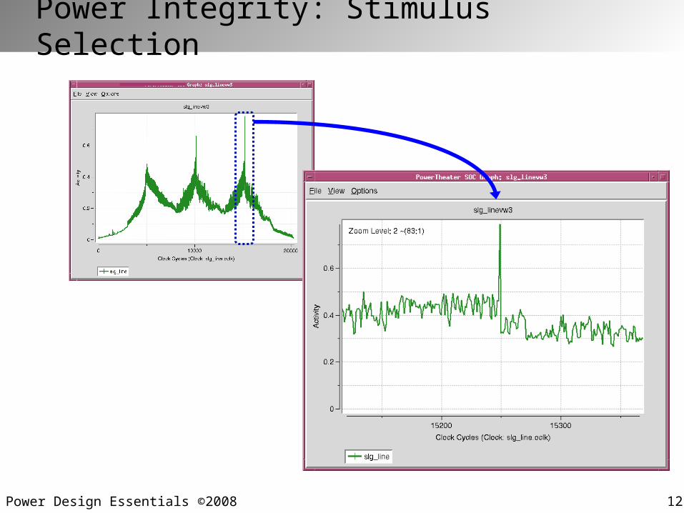
Power Integrity: Stimulus Selection
Low Power Design Essentials ©2008 12.46
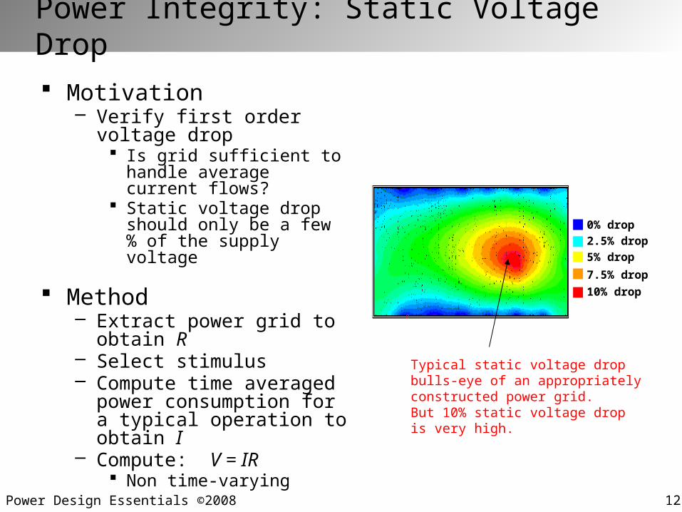
Power Integrity: Static Voltage Drop
Motivation– Verify first order voltage drop
Is grid sufficient to handle average current flows?
Static voltage drop should only be a few % of the supply voltage
Method– Extract power grid to
obtain R– Select stimulus– Compute time averaged
power consumption for a typical operation to obtain I
– Compute: V = IR Non time-varying
10% drop7.5% drop
2.5% drop0% drop
5% drop
Typical static voltage drop bulls-eye of an appropriately constructed power grid.But 10% static voltage drop is very high.
Low Power Design Essentials ©2008 12.47
Power Integrity: Dynamic Voltage Drop
Motivation– Verify dynamic voltage drop
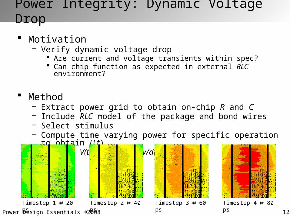
Are current and voltage transients within spec? Can chip function as expected in external RLC environment?
Method– Extract power grid to obtain on-chip R and C– Include RLC model of the package and bond wires– Select stimulus– Compute time varying power for specific operation to obtain I(t)– Compute V(t) = I(t)*R + C*dv/dt*R + L*di/dt
Timestep 1 @ 20 ps Timestep 2 @ 40 ps Timestep 3 @ 60 ps Timestep 4 @ 80 ps
Low Power Design Essentials ©2008 12.48
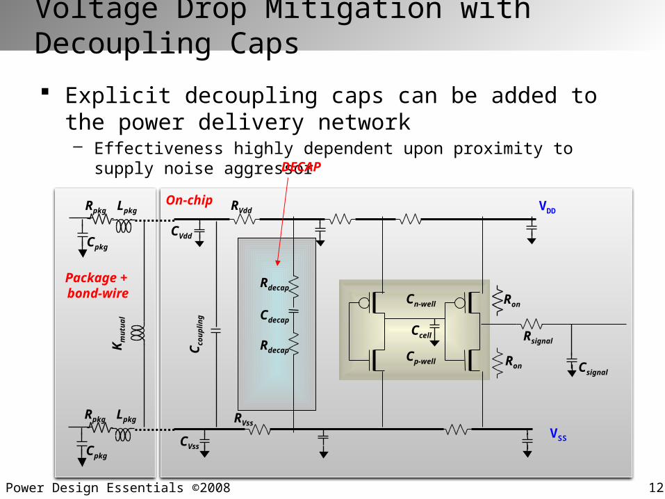
Voltage Drop Mitigation with Decoupling Caps
Explicit decoupling caps can be added to the power delivery network– Effectiveness highly dependent upon proximity to supply noise aggressor
On-chip
Ccell
Cp-well
Cn-well
Cdecap
Rdecap
Rdecap
Csignal
Ron
Ron
Rsignal
Rpkg Lpkg
Cpkg
Package + bond-wire
Rpkg Lpkg
Cpkg
Km
utua
l
RVdd
CVdd
VDD
VSSCVss
RVss
Cco
uplin
g
DECAP
Low Power Design Essentials ©2008 12.49
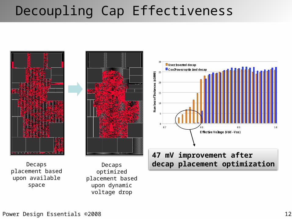
Decoupling Cap Effectiveness
0
5
10
15
20
25
30
0.7 0.8 0.9 1.0
Effective Voltage (Vdd - Vss)
Num
ber o
f Ins
tanc
es (x
1000
)
User inserted decapCoolPower optimized decap
47 mV improvement afterdecap placement optimizationDecaps placement
based upon available space
Decaps optimized placement based
upon dynamic voltage drop
Low Power Design Essentials ©2008 12.50
Dynamic Voltage Drop Impact
0
10000
20000
30000
40000
50000
60000
70000
80000
90000
-2 -1 0 1 2 3 4 5 6 7 8 9 10 11 12 13 14 15
Slack(ns)
Num
ber o
f pat
hs
0
500
1000
1500
2000
2500
3000
3500
4000
4500
-2 -1.5 -1 -0.5 0 0.5
Num
ber o
f pat
hs
Without Voltage Drop With Voltage Drop
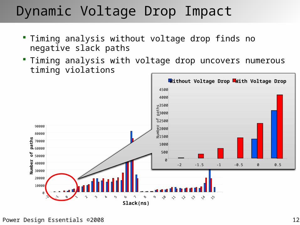
Timing analysis without voltage drop finds no negative slack paths Timing analysis with voltage drop uncovers numerous timing violations
Low Power Design Essentials ©2008 12.51
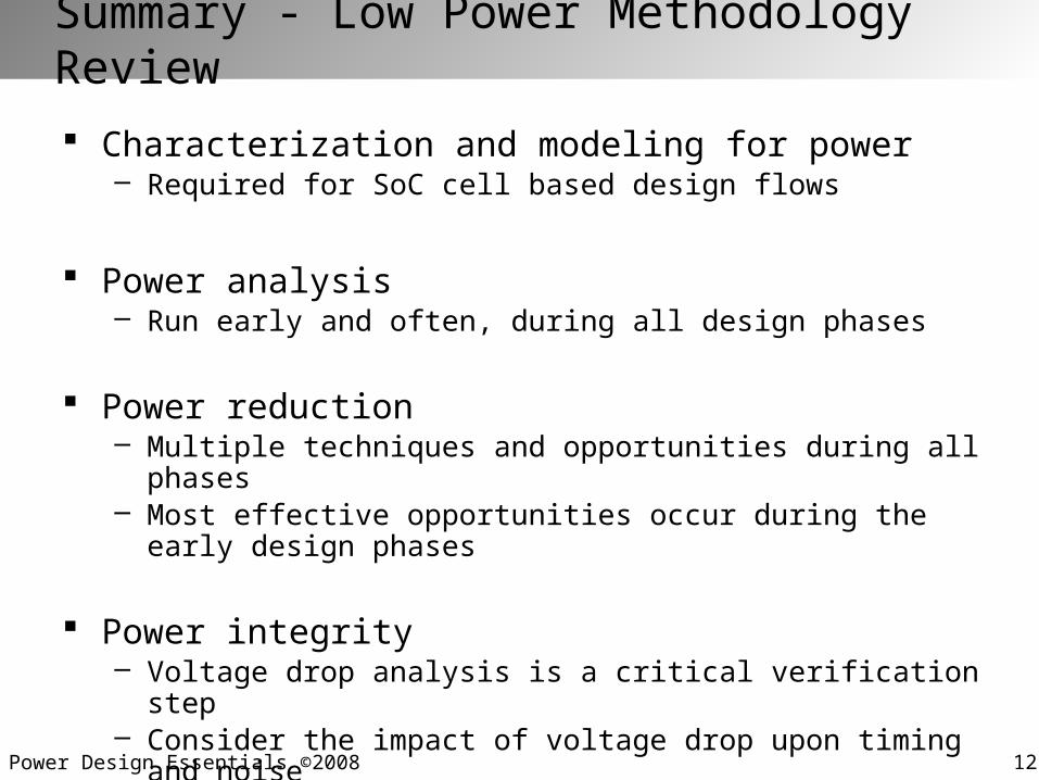
Summary - Low Power Methodology Review
Characterization and modeling for power– Required for SoC cell based design flows
Power analysis– Run early and often, during all design phases
Power reduction– Multiple techniques and opportunities during all phases– Most effective opportunities occur during the early design phases
Power integrity– Voltage drop analysis is a critical verification step– Consider the impact of voltage drop upon timing and noise
Low Power Design Essentials ©2008 12.52
Some Useful ReferencesBooks and Book Chapters A. Chandrakasan, R. Brodersen, Low Power Digital CMOS Design, Kluwer Academic Publishers, 1995. D. Chinnery, K. Keutzer, Closing the Power Gap Between ASIC and Custom, Springer, 2007. J. Frenkil, “Tools and Methodologies for Power Sensitive Design”, in Power Aware Design Methodologies, M. Pedram
and J. Rabaey, Kluwer, 2002. J. Frenkil and S. Venkatraman, “Power Gating Design Automation”, in [Chinnery, Springer’07]. M. Keating et al, Low Power Methodology Manual − For System-on-Chip Design, Springer, 2007. C. Piguet, Ed., Low-Power Electronics Design, Ch. 38-42, CRC Press, 2005
Articles and Web Sites Cadence Power Forward Initiative, http://www.cadence.com/partners/power_forward/index.aspx A. Chandrakasan, S. Sheng, and R. W. Brodersen, "Low-power Digital CMOS Design," IEEE Journal of Solid State
Circuits, pp. 473-484, April 1992. N. Dave, M. Pellauer, S. Gerding, Arvind, “802.11a Transmitter: A Case Study in Microarchitectural Exploration”,
MEMOCODE 2006. S. Gary, P. Ippolito, G. Gerosa, C. Dietz, J. Eno, H., Sanchez, “PowerPC603, A Microprocessor for Portable
Computers”, IEEE Design and Test of Computers, Volume 11, Issue 4, pp. 14-23, Winter 1994. S. Kosonocky, et. al., “Enhanced multi-threshold (MTCMOS) circuits using variable well bias”, ISLPED Proceedings,
pp. 165-169, 2001. Liberty Modeling Standard, http://www.opensourceliberty.org/resources_ccs.html#1 Sequence PowerTheatre, http://www.sequencedesign.com/solutions/powertheater.php Sequence CoolTime,
http://www.sequencedesign.com/solutions/coolproducts.php Synopsys Galaxy Power Environment, http://www.synopsys.com/products/solutions/galaxy/power/power.html Q. Wang and S. Vrudhula, “Algorithms for minimizing standby power in deep submicrometer, dual-Vt CMOS circuits,”
IEEE Transactions on Computer-Aided Design of Integrated Circuits and Systems, Vol. 21, No. 3, pp 306–318, March 2002.