Embed Size (px)
Citation preview

i iLow-Power, High-Bandwidth, and Ultra-Small Memory Module Design
Qawi I. Harvard, PhD, and R. Jacob Baker, PhDD f El i l d C E i iDepartment of Electrical and Computer Engineering

Abstract
The main memory subsystem has become inefficient. Sustaining performance gains has power consumption, capacity, and cost moving in the wrong direction. This talk proposes novel module, DRAM, and interconnect architectures in an attempt to alleviate these trends. The proposed architectures utilize inexpensive innovations, including interconnect and packaging, to substantially reduce the power, and increase the capacity and bandwidth of the main memory system. A low cost advanced packaging technology is used to propose an 8 die and
332-die memory module. The 32-die memory module measures less than 2 cm3. The size and packaging technique allow the memory module to consume less power than conventional module designs. A 4 Gb DRAM architecture utilizing 64 data pins is proposed. The DRAM architecture is inline with ITRS roadmaps and can consume 50% less power while increasing b d id h b h l b f d i d b l i ibandwidth by 100%. The large number of data pins are supported by a low power capacitive-coupled interconnect. The receivers developed for the capacitive interface were fabricated in 0.5 µm and 65 nm CMOS technologies. The 0.5 µm design operated at 200 Mbps, used a coupling capacitor of 100 fF, and consumed less than 3 pJ/bit of energy. The 65 nm design
d 4 Gb d li i f 1 f d d l h 1 f /bioperated at 4 Gbps, used a coupling capacitor of 15 fF, and consumed less than 15 fJ/bit.
2

Mobile Platform
Motorola Atrix (Front)Linear Power AmplifierLinear Power AmplifierRF Power ManagementDC Power Management
d i
3.5
mm Hard Drive
Accelerometer
< 6
3
< 117.75 mm

Mobile Platform
Motorola Atrix (Back)
Memory (DSP)Memory & CPUHSPA+ DSPHSPA+ DSP802.11n & BluetoothCompass
4
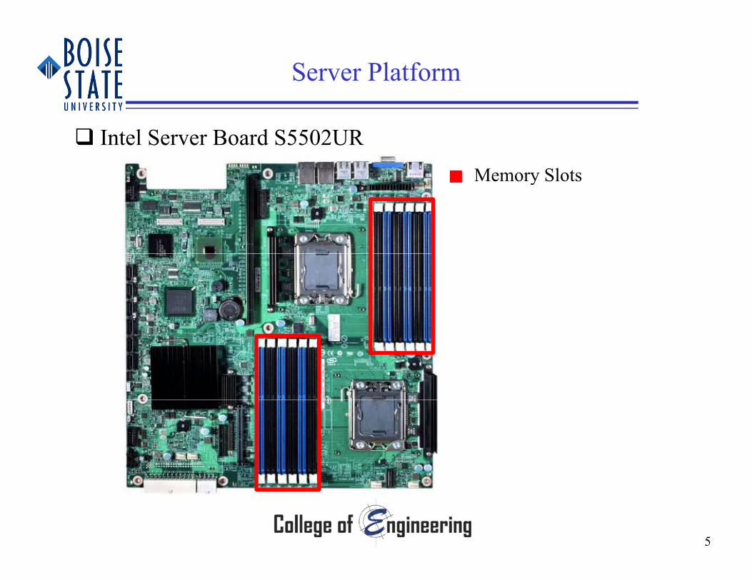
Server Platform
Intel Server Board S5502URMemory SlotsMemory Slots
5
Organization
Main Memory Limitations Nano-ModuleWide I/O DRAM Architecture High Bandwidth Interconnect Conclusions
6
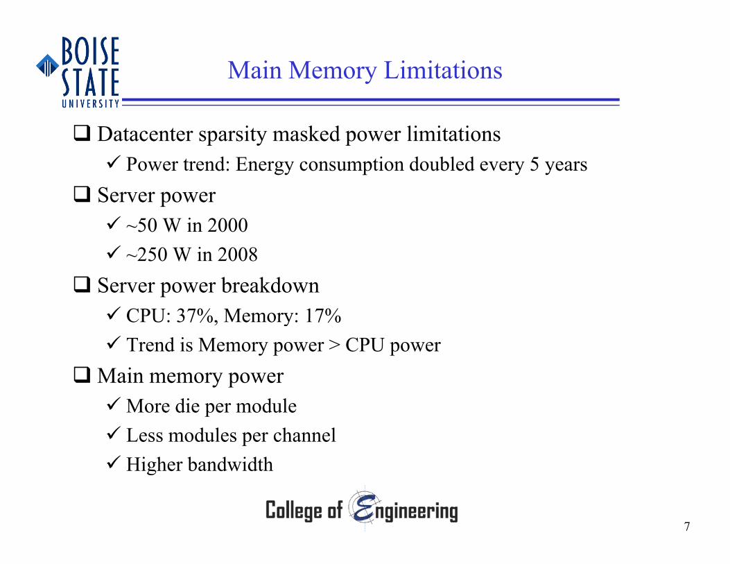
Main Memory Limitations
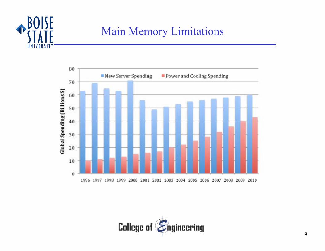
Datacenter sparsity masked power limitations Power trend: Energy consumption doubled every 5 years
Server power ~50 W in 2000 ~250 W in 2008
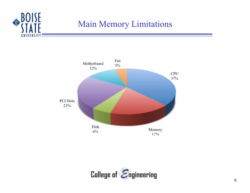
Server power breakdown CPU: 37% Memory: 17% CPU: 37%, Memory: 17% Trend is Memory power > CPU power
Main memory powerMore die per module Less modules per channel Hi h b d idth Higher bandwidth
7
Main Memory Limitations
8
Main Memory Limitations
9
Main Memory Limitations
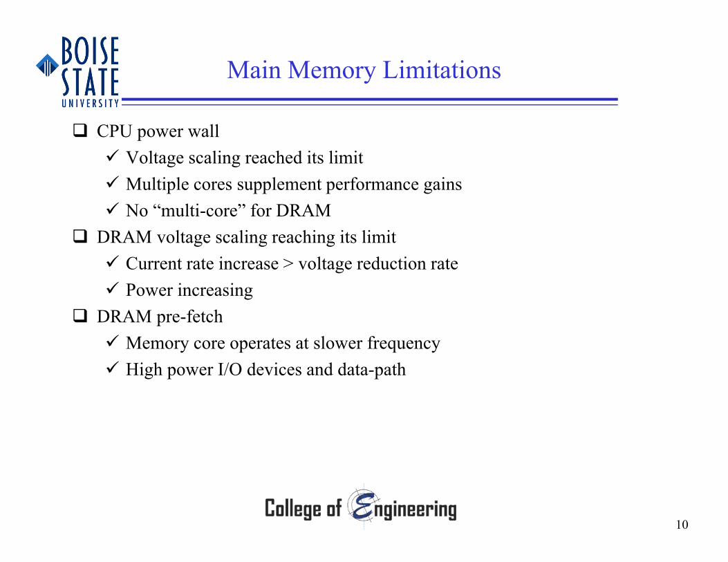
CPU power wall Voltage scaling reached its limit Multiple cores supplement performance gains No “multi-core” for DRAM
DRAM voltage scaling reaching its limitg g g Current rate increase > voltage reduction rate Power increasing
DRAM pre fetch DRAM pre-fetch Memory core operates at slower frequency High power I/O devices and data-path
10
Main Memory Limitations
11
Main Memory Limitations
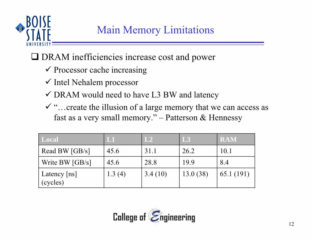
DRAM inefficiencies increase cost and power Processor cache increasing Intel Nehalem processor DRAM would need to have L3 BW and latency “ t th ill i f l th t “…create the illusion of a large memory that we can access as
fast as a very small memory.” – Patterson & Hennessy
Local L1 L2 L3 RAMRead BW [GB/s] 45.6 31.1 26.2 10.1Write BW [GB/s] 45.6 28.8 19.9 8.4[ ]Latency [ns] (cycles)
1.3 (4) 3.4 (10) 13.0 (38) 65.1 (191)
12
Main Memory Limitations
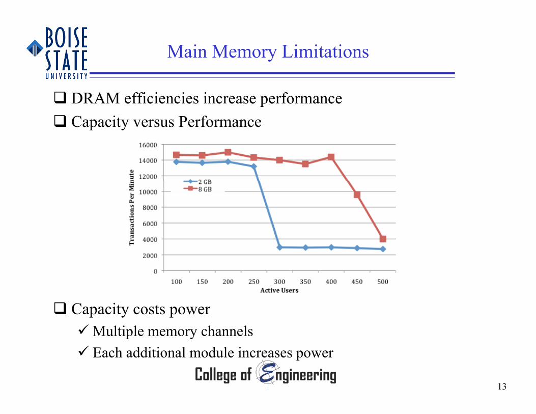
DRAM efficiencies increase performance Capacity versus Performancep y
Capacity costs powerMultiple memory channelsp y Each additional module increases power
13
Main Memory Limitations
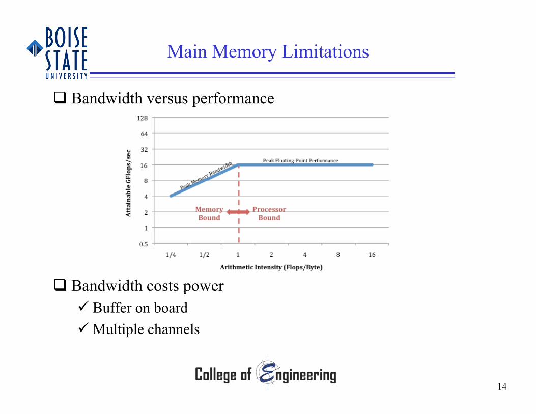
Bandwidth versus performance
Bandwidth costs power Bandwidth costs power Buffer on boardMultiple channels
14

Main Memory Limitations
DRAM inefficiencies in practice Typical video/web server motherboardyp 20+ layer PCB 6 memory channels
RDIMM 10+ layer PCBMaximum comp countMaximum comp. count
15
Main Memory Limitations
12 RDIMM Termination
o 36 components per DIMMo 8 I/O per componento 2 7 W of termination power for a read/write per moduleo 2.7 W of termination power for a read/write per moduleo 32.4 W total termination power
Wordline firingo 100 ns activation rateo 8126 page sizeo 200 fF per bitlinepo 11.2 W total bitline sense amplifier power
Sustaining performance gains through capacity and bandwidth i d t i ti i dincreases power and cost – innovation required.
16
Nano-Module
Goals Purpose was to move labs into prototype generation Required low cost, high bandwidth, and low power memory
solution that can be used with capacitive coupled interconnects in advanced server architecturesin advanced server architectures
Module component count trends required a new approach Nano-module proposed Low cost advanced packaging technology Off-the-shelf memory components
R l b l d Results can be leveraged NANDMobileMobile
17

Nano-Module
Literature review of high capacity memory stacks 1990’sMultichip Modules
o Realized planar space limitations V l & L i Val & Lemione Irvine Sensors
Solutions proposed in research Solutions proposed in research No industry due to memory hierarchy effectiveness
18
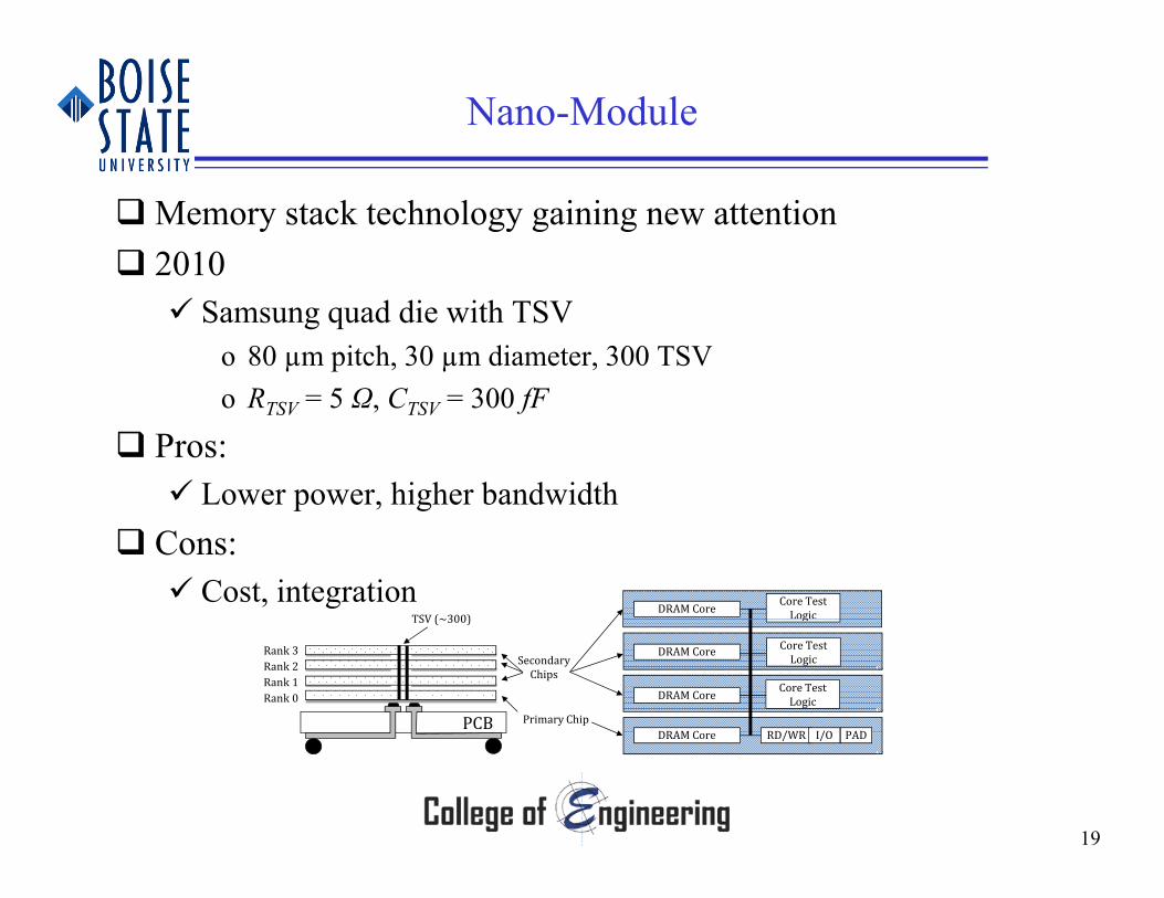
Nano-Module
Memory stack technology gaining new attention 2010 Samsung quad die with TSV
o 80 µm pitch, 30 µm diameter, 300 TSVR 5 Ω C 300 fFo RTSV = 5 Ω, CTSV = 300 fF
Pros: Lower power, higher bandwidthp , g
Cons: Cost, integration
TSV (~300)DRAMCore CoreTest
Logic
PCB PrimaryChip
SecondaryChips
TSV(~300)
Rank0Rank1Rank2Rank3
DRAM C
DRAMCore
DRAMCore
RD/WR I/O PAD
CoreTestLogic
g
CoreTestLogic
19
DRAMCore RD/WR I/O PAD
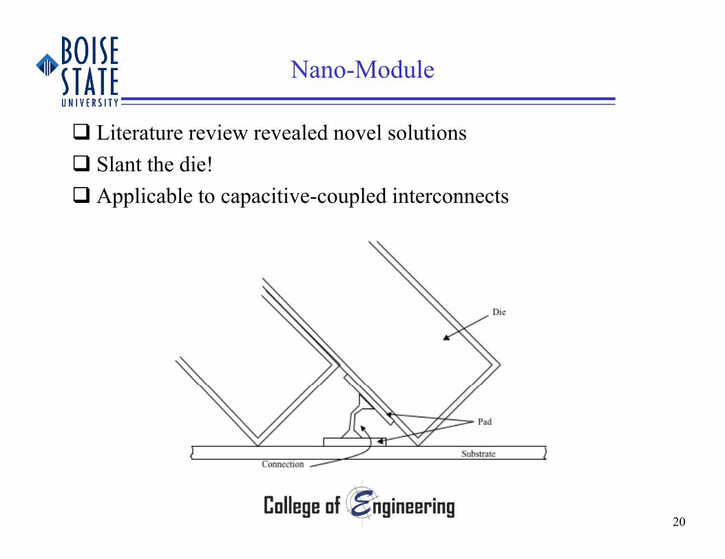
Nano-Module
Literature review revealed novel solutions Slant the die! Applicable to capacitive-coupled interconnects
20
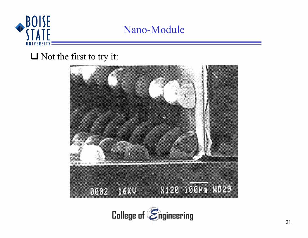
Nano-Module
Not the first to try it:
21
Nano-Module
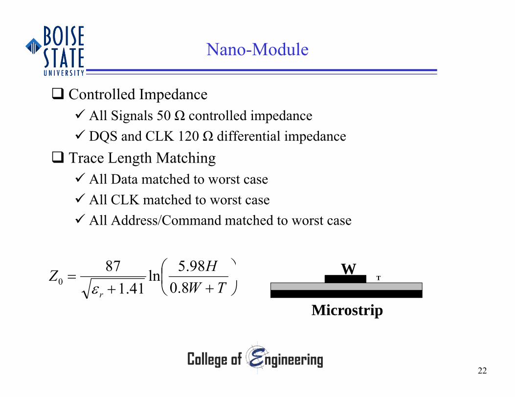
Controlled Impedance All Signals 50 Ω controlled impedance DQS and CLK 120 Ω differential impedance
Trace Length Matching All Data matched to worst case All CLK matched to worst case All Address/Command matched to worst caseAll Address/Command matched to worst case
HZ 98.5ln87 W
TW
Zr 8.0
ln41.10
WT
Microstrip
22
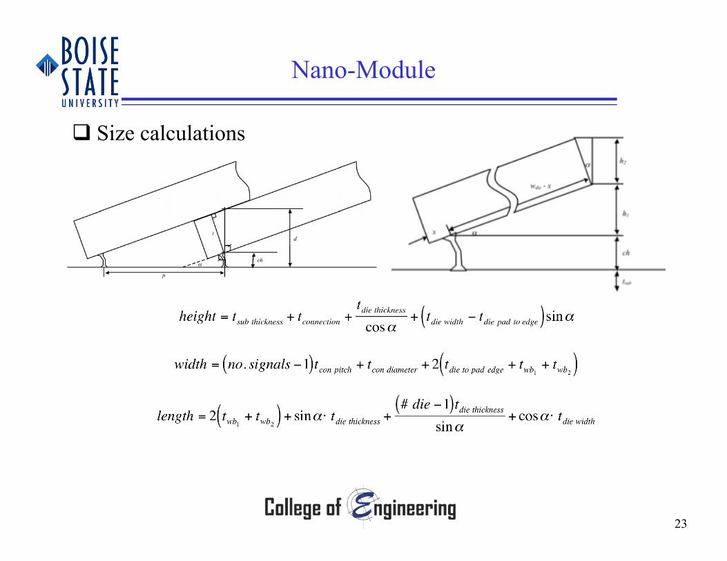
Nano-Module
Size calculations
23
Nano-Module
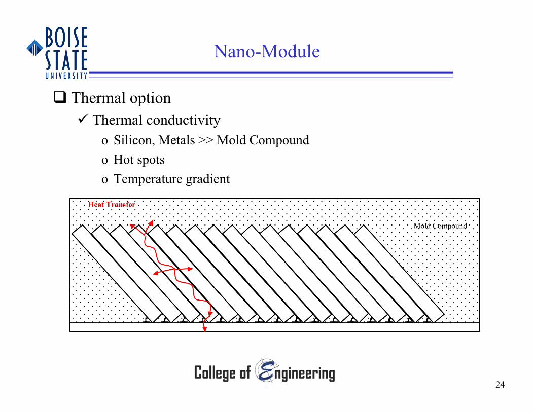
Thermal option Thermal conductivity
o Silicon, Metals >> Mold Compoundo Hot spotso Temperature gradiento Temperature gradient
24
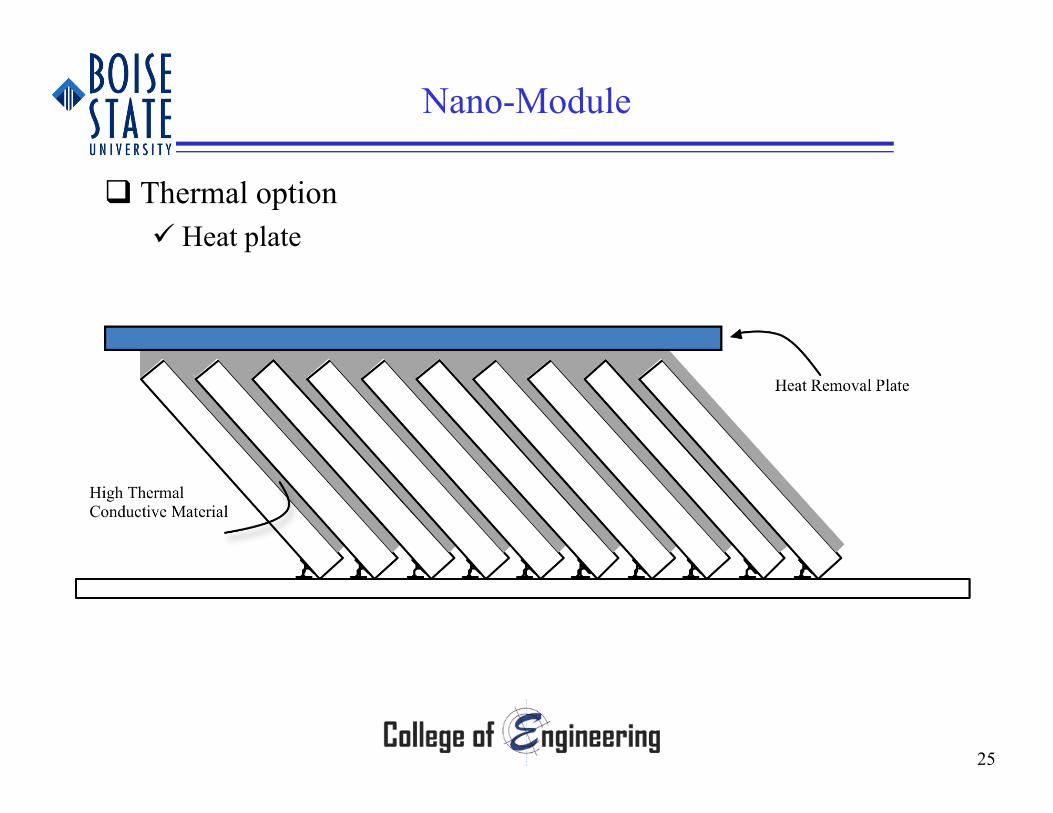
Nano-Module
Thermal option Heat plate
25
Wide I/O DRAM Architecture
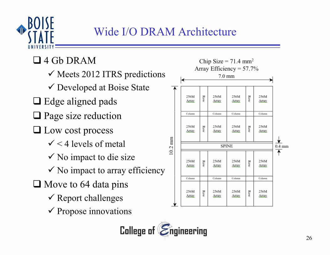
4 Gb DRAMMeets 2012 ITRS predictions Developed at Boise State
Edge aligned pads Page size reduction Low cost process < 4 levels of metal < 4 levels of metal No impact to die size No impact to array efficiency
Move to 64 data pins Report challenges i i Propose innovations
26
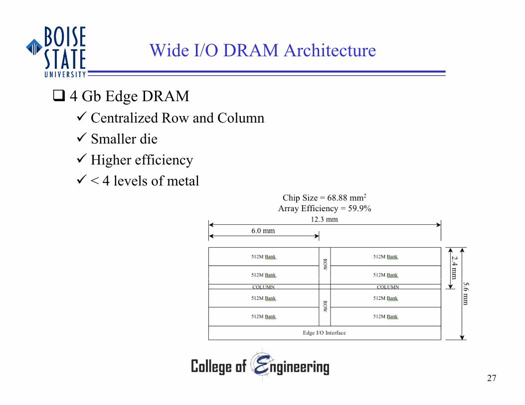
Wide I/O DRAM Architecture
4 Gb Edge DRAM Centralized Row and Column Smaller die Higher efficiency 4 l l f t l < 4 levels of metal
27
Wide I/O DRAM Architecture
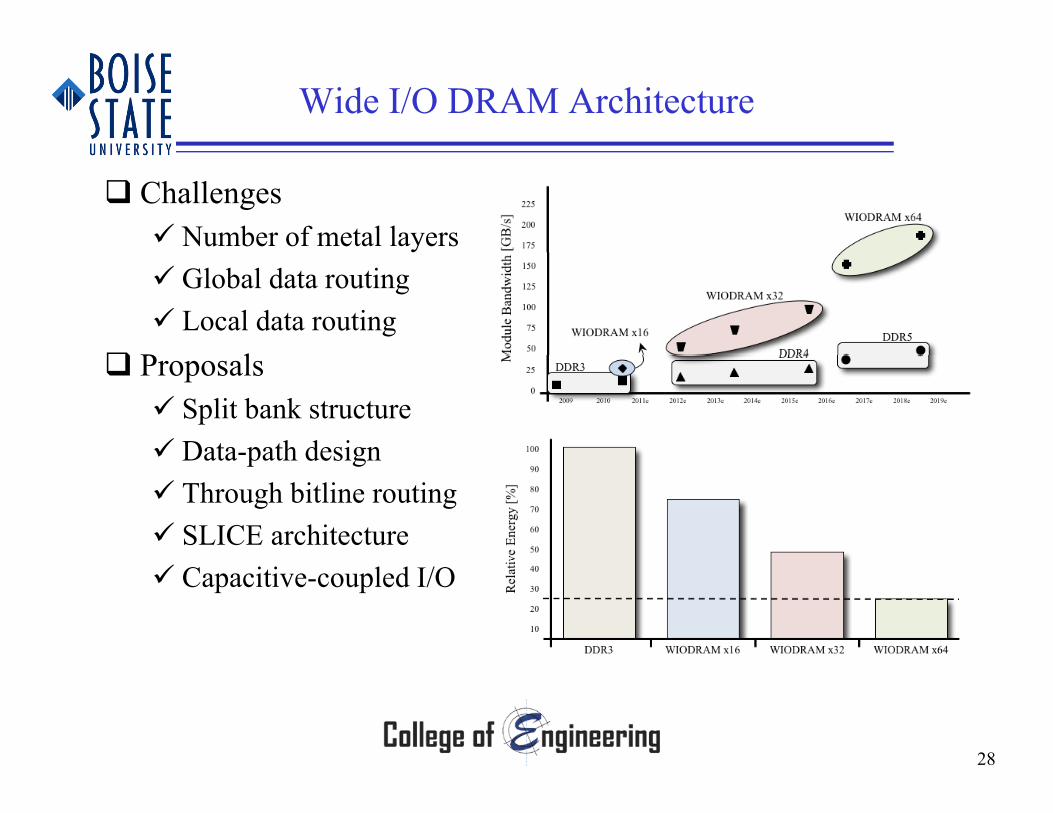
Challenges Number of metal layers Global data routing Local data routing
P l Proposals Split bank structure Data-path designData path design Through bitline routing SLICE architecture Capacitive-coupled I/O
28

High Bandwidth Interconnect
Capacitive-coupling Increased bandwidth
o Reduced ESD capacitanceo Smaller I/O channel = more I/Oo Removal of inductive channelo Removal of inductive channel
Low powero Reduced ESD capacitanceo Low power Tx & Rx
Low costo Simpleo Simple
Alignment required Literature review Revealed inefficiencies and lack of application
29
High Bandwidth Interconnect
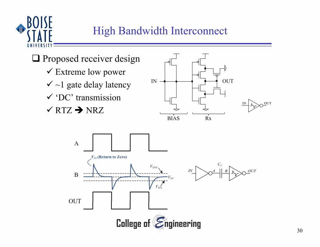
Proposed receiver design Extreme low power ~1 gate delay latency ‘DC’ transmission RTZ NRZ RTZ NRZ
30
High Bandwidth Interconnect
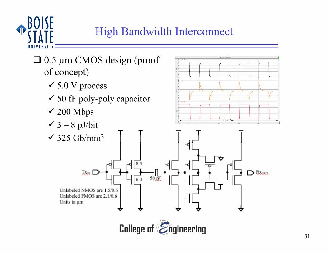
0.5 µm CMOS design (proof of concept) 5.0 V process 50 fF poly-poly capacitor 200 Mbps 200 Mbps 3 – 8 pJ/bit 325 Gb/mm2
31
High Bandwidth Interconnect
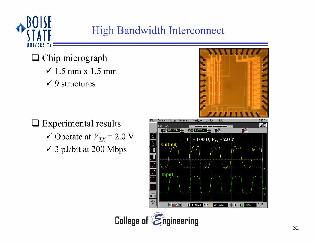
Chip micrograph 1.5 mm x 1.5 mm 9 structures
Experimental results Operate at V = 2 0 V Operate at VTX 2.0 V 3 pJ/bit at 200 Mbps
OutputCC =100fF,VTX =2.0V
Input
32
High Bandwidth Interconnect
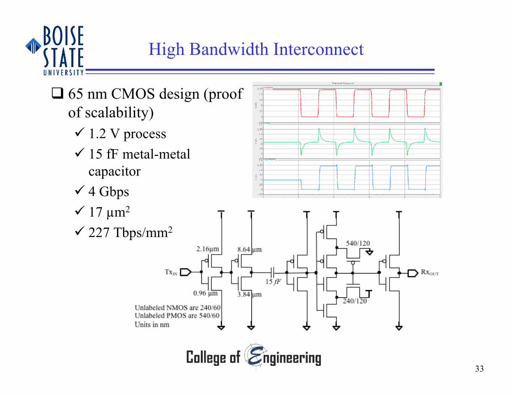
65 nm CMOS design (proof of scalability) 1.2 V process 15 fF metal-metal
capacitorcapacitor 4 Gbps 17 µm2
227 Tbps/mm2
33
High Bandwidth Interconnect
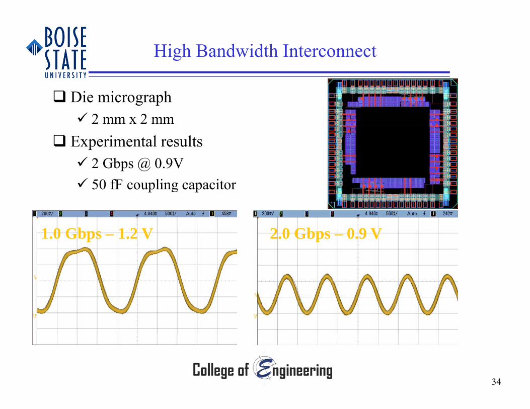
Die micrograph 2 mm x 2 mm
Experimental results 2 Gbps @ 0.9V 50 fF coupling capacitor
2 0 Gb 0 9 V1 0 Gb 1 2 V 2.0 Gbps – 0.9 V 1.0 Gbps – 1.2 V
34
High Bandwidth Interconnect
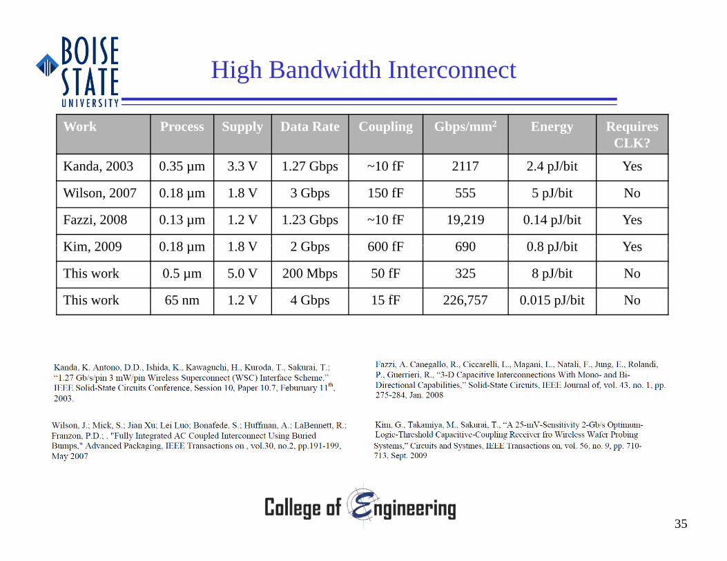
Work Process Supply Data Rate Coupling Gbps/mm2 Energy Requires CLK?
Kanda, 2003 0.35 µm 3.3 V 1.27 Gbps ~10 fF 2117 2.4 pJ/bit Yes
Wilson, 2007 0.18 µm 1.8 V 3 Gbps 150 fF 555 5 pJ/bit No
Fazzi, 2008 0.13 µm 1.2 V 1.23 Gbps ~10 fF 19,219 0.14 pJ/bit Yes
Kim 2009 0 18 µm 1 8 V 2 Gbps 600 fF 690 0 8 pJ/bit YesKim, 2009 0.18 µm 1.8 V 2 Gbps 600 fF 690 0.8 pJ/bit Yes
This work 0.5 µm 5.0 V 200 Mbps 50 fF 325 8 pJ/bit No
This work 65 nm 1.2 V 4 Gbps 15 fF 226,757 0.015 pJ/bit No
35
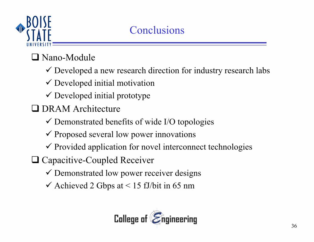
Conclusions
Nano-Module Developed a new research direction for industry research labs Developed initial motivation Developed initial prototype
DRAM A hi DRAM Architecture Demonstrated benefits of wide I/O topologies Proposed several low power innovationsProposed several low power innovations Provided application for novel interconnect technologies
Capacitive-Coupled Receiver Demonstrated low power receiver designs Achieved 2 Gbps at < 15 fJ/bit in 65 nm
36
Questions
??
37
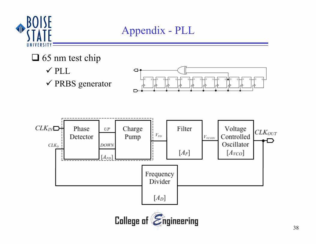
Appendix - PLL
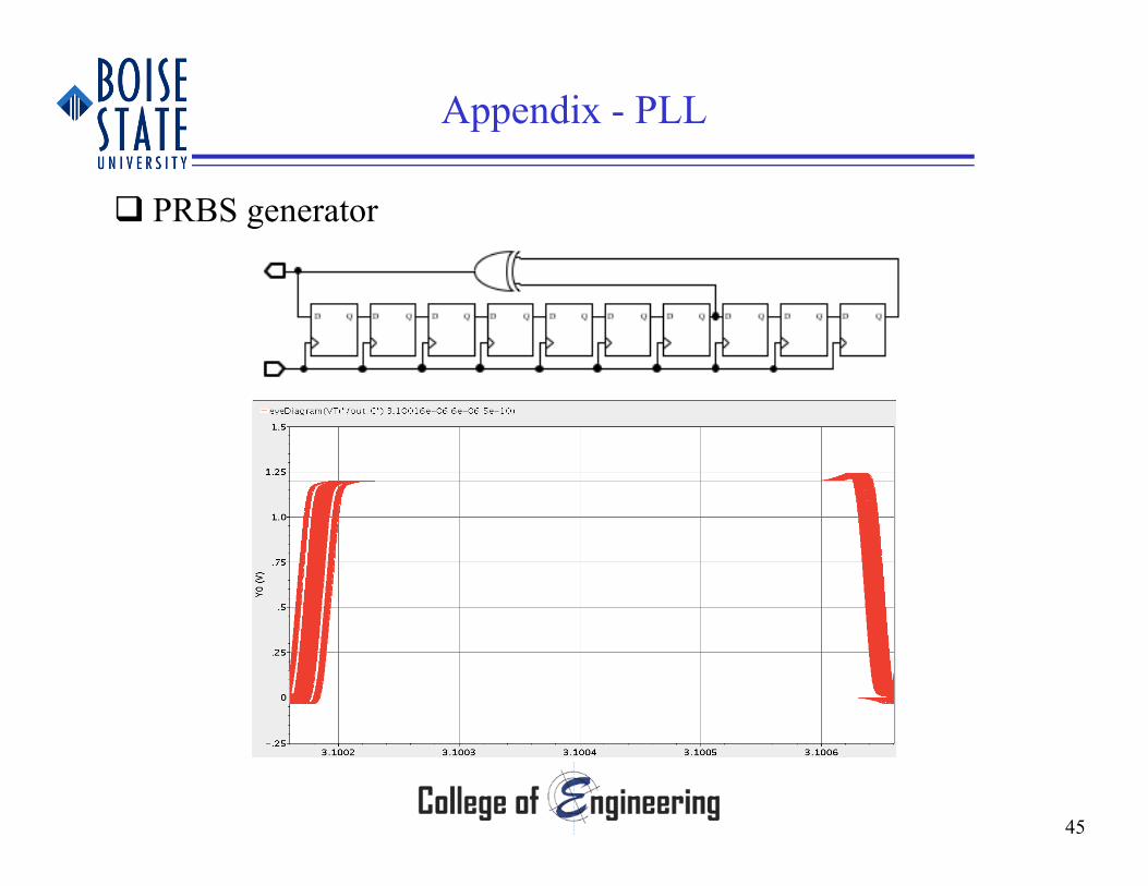
65 nm test chip PLL PRBS generator
38
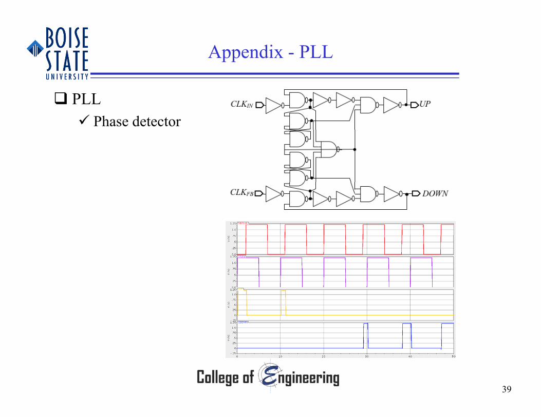
Appendix - PLL
PLL Phase detector
39
Appendix - PLL
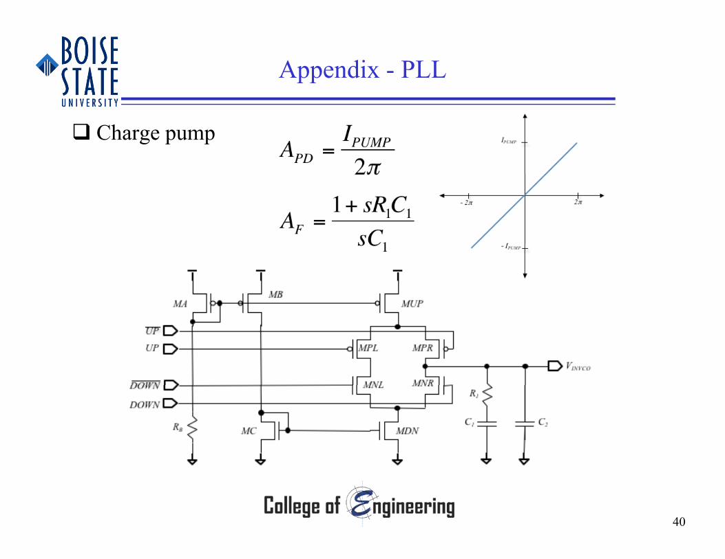
Charge pump
40
Appendix - PLL
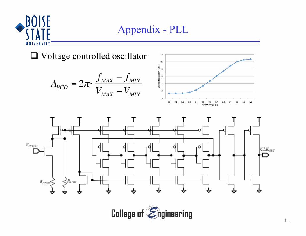
Voltage controlled oscillator
41
Appendix - PLL
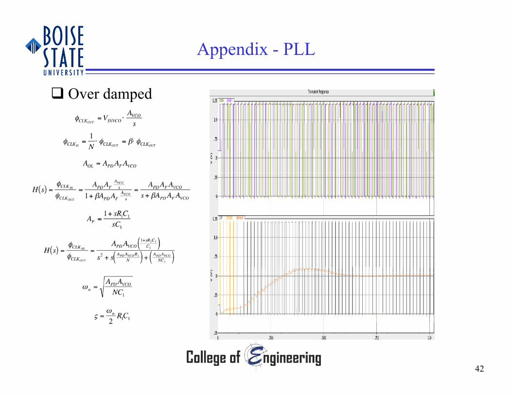
Over damped
42
Appendix - PLL
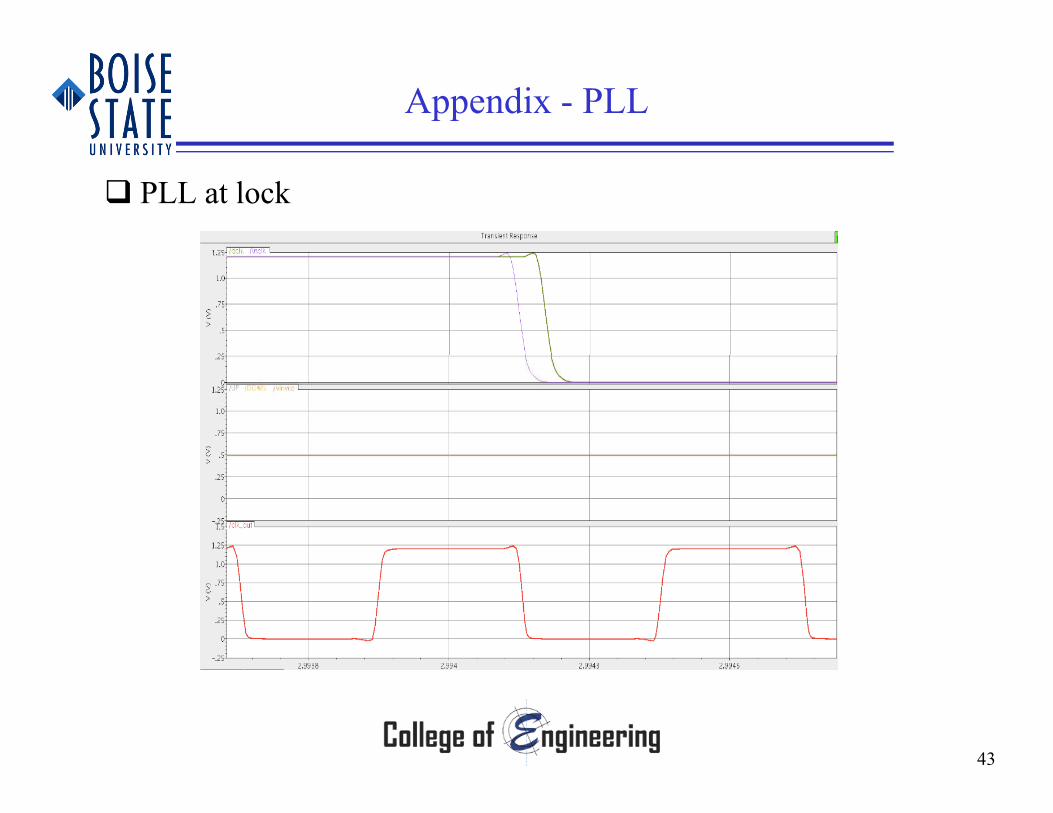
PLL at lock
43
Appendix - PLL
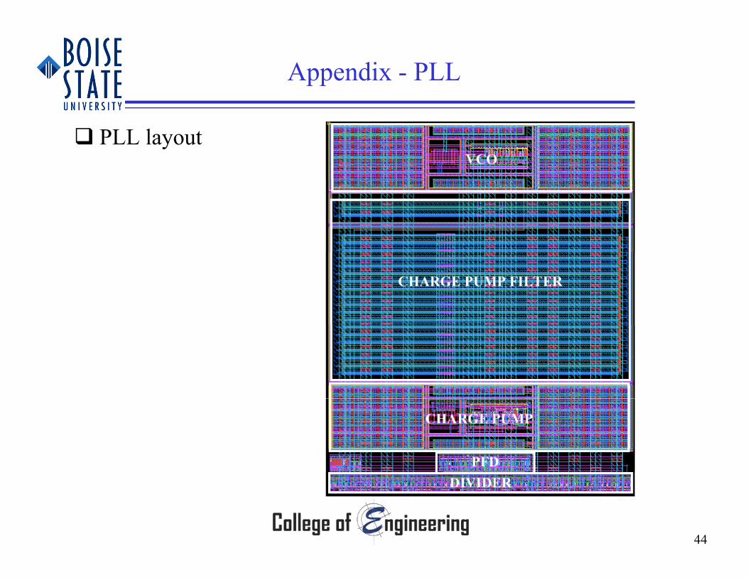
PLL layout
44
Appendix - PLL
PRBS generator
45
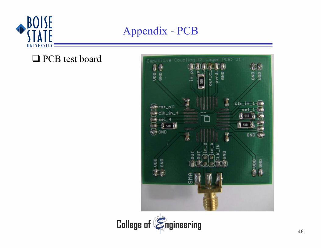
Appendix - PCB
PCB test board
46

Appendix – Dead Bug
47
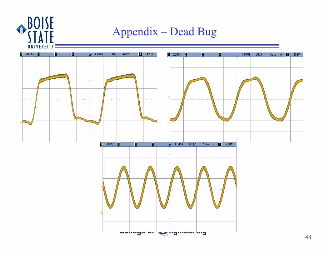
Appendix – Dead Bug
48

Appendix – 65 nm Chip
49
References
[1] Val, C.; Lemoine, T.; , "3-D interconnection for ultra-dense multichip modules," Components, Hybrids, and Manufacturing Technology, IEEE Transactions on , vol.13, no.4, pp.814-821, Dec 1990
[2] Bertin, C.L.; Perlman, D.J.; Shanken, S.N.; , "Evaluation of a three-dimensional memory cube system," Components, Hybrids, and Manufacturing Technology, IEEE Transactions on , vol.16, no.8, pp.1006-1011, Dec 1993
[3] Uksong Kang; Hoe-Ju Chung; Seongmoo Heo; Duk-Ha Park; Hoon Lee; Jin Ho Kim; Soon-Hong Ahn; Soo-Ho Cha; Jaesung Ahn; DukMin Kwon; Jae-Wook Lee; Han-Sung Joo; Woo-Seop Kim; Dong Hyeon Jang; Nam Seog Kim; Jung-Hwan Choi; Tae-GyeongChung; Jei-Hwan Yoo; Joo Sun Choi; Changhyun Kim; Young-Hyun Jun; , "8 Gb 3-D DDR3 DRAM Using Through-Silicon-Via Technology," Solid-State Circuits, IEEE Journal of , vol.45, no.1, pp.111-119, Jan. 2010
[4] Matthias, T.; Kim, B.; Burgstaller, D.; Wimplinger, M.; Lindner, P., “State-of-the-art Thin Wafer Processing,” Chip Scale Review, vol. 14, no. 4, pp. 26, July 2010., , pp , y
[5] U.S. Enviornmental Protection Agency, “Report to Congress on Server and Data Center Energy Efficiency Public Law 109-431,” 2007.[6] L. Minask, B. Ellison, “The Problem of Power Consumption in Servers,” Intel Press, 2009,
http://www.intel.com/intelpress/articles/rpcs1.htm[7] D. Patterson, J. Hennessy, Computer Organization and Design, 4th ed., Morgan Kaufmann Publishers, San Francisco, 2009.[8] Karp, J.; Regitz, W.; Chou, S.; , "A 4096-bit dynamic MOS RAM," Solid-State Circuits Conference. Digest of Technical Papers. 1972 [ ] p, ; g , ; , ; , y , f g f p
IEEE International , vol.XV, no., pp. 10- 11, Feb 1972[9] Micron Technology Inc. Various Datasheets: http://www.micron.com/products/dram/[10] B. Gervasi, “ Time to Rethink DDR4,” MEMCON 2010, http://discobolusdesigns.com/personal/20100721a_gervasi_rethinking_ddr4.pdf[11] Various IBM datasheets. www.ibm.com[12] “Power-Efficiency with 2, 4, 6, and 8 Gigabytes of Memory for Intel and AMD Servers,” Neal Nelson & Associates, White Paper 2007.[ ] y , , , g y y , , p[13] Rambus, “Challenges and Solutions for Future Main Memory,”
http://www.rambus.com/assests/documents/products/future_main_memory_whitepaper.pdf, May 2009.[14] Intel AMB Datasheet, http://www.intel.com/assets/pdf/datasheet/313072.pdf, pg 38.
50
References
[15] “Intel Server Board S5520UR and SS5520URT, Technical Product Specification” Rev. 1.6, July 2010, Intel Corporation.[16] D. Klein, “The Future of Memory and Storage: Closing the Gap,” Microsoft WinHEC 2007, May 2007.[17] Cotues, “Stepped Electronic Device Package,” U.S. Patent 5,239,447, Aug. 24, 1993.[18] G. Rinne, P. Deane, “Microelectronic Packaging Using Arched Solder Columns,” U.S. Patent 5,963,793, Oct. 5, 1999.[19] R. Plieninger, “Challenges and New Solutions for High Integration IC Packaging,” ESTC, July 2006, http://141.30.122.65/Keynotes/6-
Plieninger-ESTC_Keynote_20060907.pdf[20] Harvard, Q., "Wide I/O Dram Architecture Utilizing Proximity Communication" (2009). Boise State University Theses and Dissertations.
Paper 72.[21] International Technology Roadmap for Semiconductor, 2007 Edition, http://www.itrs.net/Links/2007ITRS/Home2007.htm, 2007.[22] K. Kilbuck, “Main Memory Technology Direction,” Microsoft WinHEC 2007, May 2007. [23] R. Drost, R. Hopkins, I. Sutherland, “Proximity Communication,” Proceedings of the IEEE 2003 Custom Integrated Circuits Conference,
vol. 39, issue 9, pp. 469-472, September 2003.[24] Saltzman, D.; Knight, T., Jr., "Capacitive coupling solves the known good die problem," Multi-Chip Module Conference, 1994. MCMC-
94, Proceedings., 1994 IEEE , vol., no., pp.95-100, 15-17 Mar 1994[25] S l D K i h T J F P "A li i f i i li i h f b i " M l i Chi M d l C f 1995[25] Salzman, D.; Knight, T., Jr.; Franzon, P., "Application of capacitive coupling to switch fabrics," Multi-Chip Module Conference, 1995.
MCMC-95, Proceedings., 1995 IEEE , vol., no., pp.195-199, 31 Jan-2 Feb 1995[26] Wilson, J.; Mick, S.; Jian Xu; Lei Luo; Bonafede, S.; Huffman, A.; LaBennett, R.; Franzon, P.D.; , "Fully Integrated AC Coupled
Interconnect Using Buried Bumps," Advanced Packaging, IEEE Transactions on , vol.30, no.2, pp.191-199, May 2007[27] Luo, L.; Wilson, J.M.; Mick, S.E.; Jian Xu; Liang Zhang; Franzon, P.D.; , "3 gb/s AC coupled chip-to-chip communication using a low
swing pulse receiver " Solid-State Circuits IEEE Journal of vol 41 no 1 pp 287- 296 Jan 2006swing pulse receiver, Solid State Circuits, IEEE Journal of , vol.41, no.1, pp. 287 296, Jan. 2006[28] R. Baker, CMOS: Circuit Design, Layout, and Simulation, Third Edition, Wiley-IEEE, 2010[29] O. Schwartsglass, “PRBS Work,” The Hebrew University of Jerusalem, VLSI class notes, 2002.
http://www.cs.huji.ac.il/course/2002/vlsilab/files/prbs/PRBS.pdf
51