Embed Size (px)
Citation preview

Low Power Integrated LC Voltage ControlledOscillator in CMOS Technology at 900MHz
Por
Rafaella Fiorelli
Tesis Presentada Ante elInstituto de Ingenierıa Electrica
Para Cumplir con Parte delos Requisitos del Grado de
MAGISTER EN INGENIERıA ELECTRICA
En el Area de MICROELECTRONICA
Tutor:
Prof. Dr.Fernando Silveira
Tribunal:
Prof.Dr.Wilhelmus Van Noije, USP, Brazil
Prof. Juan Martony, UdelaR, Uruguay
MSc.Julio Perez Acle, UdelaR, Uruguay
Instituto de Ingenierıa ElectricaFacultad de Ingenierıa
Universidad de la RepublicaMontevideo, Uruguay
December 2005

ISSN: 1510-7264
Typesetted in LATEX2ε
Contents
List of Figures . . . . . . . . . . . . . . . . . . . . . . . . . . . . . . . . . . . vi
List of Tables . . . . . . . . . . . . . . . . . . . . . . . . . . . . . . . . . . . . ix
Resumen . . . . . . . . . . . . . . . . . . . . . . . . . . . . . . . . . . . . . . x
Abstract . . . . . . . . . . . . . . . . . . . . . . . . . . . . . . . . . . . . . . . xi
Agradecimientos . . . . . . . . . . . . . . . . . . . . . . . . . . . . . . . . . . xiii
1. Introduction . . . . . . . . . . . . . . . . . . . . . . . . . . . . . . . . . . . 1
2. Analysis and design of -Gm LC VCOs . . . . . . . . . . . . . . . . . . . . 5
2.1 Introduction . . . . . . . . . . . . . . . . . . . . . . . . . . . . . . . . 5
2.2 Principles and Topologies of -Gm LC VCO . . . . . . . . . . . . . . . 5
2.3 Cross-coupled transistors block . . . . . . . . . . . . . . . . . . . . . 10
2.4 Complementary cross-coupled -Gm LC VCO . . . . . . . . . . . . . . 13
2.5 Design Methodology . . . . . . . . . . . . . . . . . . . . . . . . . . . 15
2.6 Amplitude stabilization mechanism . . . . . . . . . . . . . . . . . . . 19
2.7 Moderate inversion design . . . . . . . . . . . . . . . . . . . . . . . . 21
2.8 Layout design and its consequences in the design methodology . . . . 22
2.9 Current Source design . . . . . . . . . . . . . . . . . . . . . . . . . . 24
2.10 Final Design . . . . . . . . . . . . . . . . . . . . . . . . . . . . . . . . 25
3. Phase Noise in LC VCOs . . . . . . . . . . . . . . . . . . . . . . . . . . . . 33
3.1 Introduction . . . . . . . . . . . . . . . . . . . . . . . . . . . . . . . . 33
3.2 Phase Noise Definition . . . . . . . . . . . . . . . . . . . . . . . . . . 33
3.3 Review of existing Phase Noise Models . . . . . . . . . . . . . . . . . 34
3.3.1 Linear time invariant model . . . . . . . . . . . . . . . . . . . 34
3.3.2 A linear time varying phase noise theory . . . . . . . . . . . . 37
3.4 Noise Sources . . . . . . . . . . . . . . . . . . . . . . . . . . . . . . . 42
3.5 Trade-offs in -Gm LC VCOs . . . . . . . . . . . . . . . . . . . . . . . 44
3.6 Phase Noise results obtained from simulation . . . . . . . . . . . . . . 48
3.7 Conclusions . . . . . . . . . . . . . . . . . . . . . . . . . . . . . . . . 50
iii
4. Inductors Design . . . . . . . . . . . . . . . . . . . . . . . . . . . . . . . . 53
4.1 Introduction . . . . . . . . . . . . . . . . . . . . . . . . . . . . . . . . 53
4.2 Inductor Types . . . . . . . . . . . . . . . . . . . . . . . . . . . . . . 53
4.3 Modelling . . . . . . . . . . . . . . . . . . . . . . . . . . . . . . . . . 54
4.4 Inductor losses . . . . . . . . . . . . . . . . . . . . . . . . . . . . . . 58
4.4.1 Metal Losses . . . . . . . . . . . . . . . . . . . . . . . . . . . . 58
4.4.2 Substrate Losses . . . . . . . . . . . . . . . . . . . . . . . . . 59
4.5 VCO Phase noise and Inductor . . . . . . . . . . . . . . . . . . . . . 60
4.6 Simulation tools . . . . . . . . . . . . . . . . . . . . . . . . . . . . . . 61
4.7 Inductor Design . . . . . . . . . . . . . . . . . . . . . . . . . . . . . . 63
5. Varactor Design . . . . . . . . . . . . . . . . . . . . . . . . . . . . . . . . . 69
5.1 Introduction . . . . . . . . . . . . . . . . . . . . . . . . . . . . . . . . 69
5.2 Varactors topologies . . . . . . . . . . . . . . . . . . . . . . . . . . . 69
5.3 Quality factor and Parasitic Resistance of the I-MOS varactor . . . . 75
5.4 Final Varactor Design . . . . . . . . . . . . . . . . . . . . . . . . . . 76
5.5 Conclusions . . . . . . . . . . . . . . . . . . . . . . . . . . . . . . . . 79
6. Measurements . . . . . . . . . . . . . . . . . . . . . . . . . . . . . . . . . . 81
6.1 Introduction . . . . . . . . . . . . . . . . . . . . . . . . . . . . . . . . 81
6.2 Measurement Setup . . . . . . . . . . . . . . . . . . . . . . . . . . . . 81
6.3 PSD measurements . . . . . . . . . . . . . . . . . . . . . . . . . . . . 83
6.4 Phase noise measurements . . . . . . . . . . . . . . . . . . . . . . . . 84
6.5 Conclusions . . . . . . . . . . . . . . . . . . . . . . . . . . . . . . . . 86
7. Conclusions and Future Work . . . . . . . . . . . . . . . . . . . . . . . . . 87
7.1 Introduction . . . . . . . . . . . . . . . . . . . . . . . . . . . . . . . . 87
7.2 Challenges of designing an on-chip low power VCO . . . . . . . . . . 87
7.3 Key features of the proposed VCO . . . . . . . . . . . . . . . . . . . 88
7.4 Moderate inversion and design methodology . . . . . . . . . . . . . . 88
7.5 Measurement difficulties . . . . . . . . . . . . . . . . . . . . . . . . . 88
7.6 Final conclusions and future work . . . . . . . . . . . . . . . . . . . . 89
iv
A. . . . . . . . . . . . . . . . . . . . . . . . . . . . . . . . . . . . . . . . . . . 91
A.1 Relation between the bandwidth of the tank impedance and the tankquality factor . . . . . . . . . . . . . . . . . . . . . . . . . . . . . . . 91
A.2 Phase Noise vs. the transconductance-to-current ratio . . . . . . . . . 92
A.3 Equivalence between the inductor series resistance and the parallelresistance . . . . . . . . . . . . . . . . . . . . . . . . . . . . . . . . . 92
A.4 Deduction of the Rsi,ox and Csi,ox values . . . . . . . . . . . . . . . . 94
A.5 I-MOS varactor Gate capacitance versus i . . . . . . . . . . . . . . . 95
B. . . . . . . . . . . . . . . . . . . . . . . . . . . . . . . . . . . . . . . . . . . 97
B.1 Comparison of the phase noise performance of a all-nMOS LC VCOand of a complementary LC VCO . . . . . . . . . . . . . . . . . . . 97
C. . . . . . . . . . . . . . . . . . . . . . . . . . . . . . . . . . . . . . . . . . . 101
C.1 Layout of the PCB . . . . . . . . . . . . . . . . . . . . . . . . . . . . 101
Bibliography . . . . . . . . . . . . . . . . . . . . . . . . . . . . . . . . . . . . 104
v

List of Figures
2.1 Typical curve of the VCO frequency versus Vbias . . . . . . . . . . . . . 6
2.2 Types of oscillator models . . . . . . . . . . . . . . . . . . . . . . . . . 7
2.3 Different topologies of -Gm LC VCO . . . . . . . . . . . . . . . . . . . 9
2.4 Small signal cross-coupled block models . . . . . . . . . . . . . . . . . . 12
2.5 Complementary VCO topology used in this work . . . . . . . . . . . . . 13
2.6 Small signal quasi-static cross-coupled complementary VCO model . . . 14
2.7 gm/ID vs. ID/(W/L) measured and estimated . . . . . . . . . . . . . . 16
2.8 Design methodology . . . . . . . . . . . . . . . . . . . . . . . . . . . . . 17
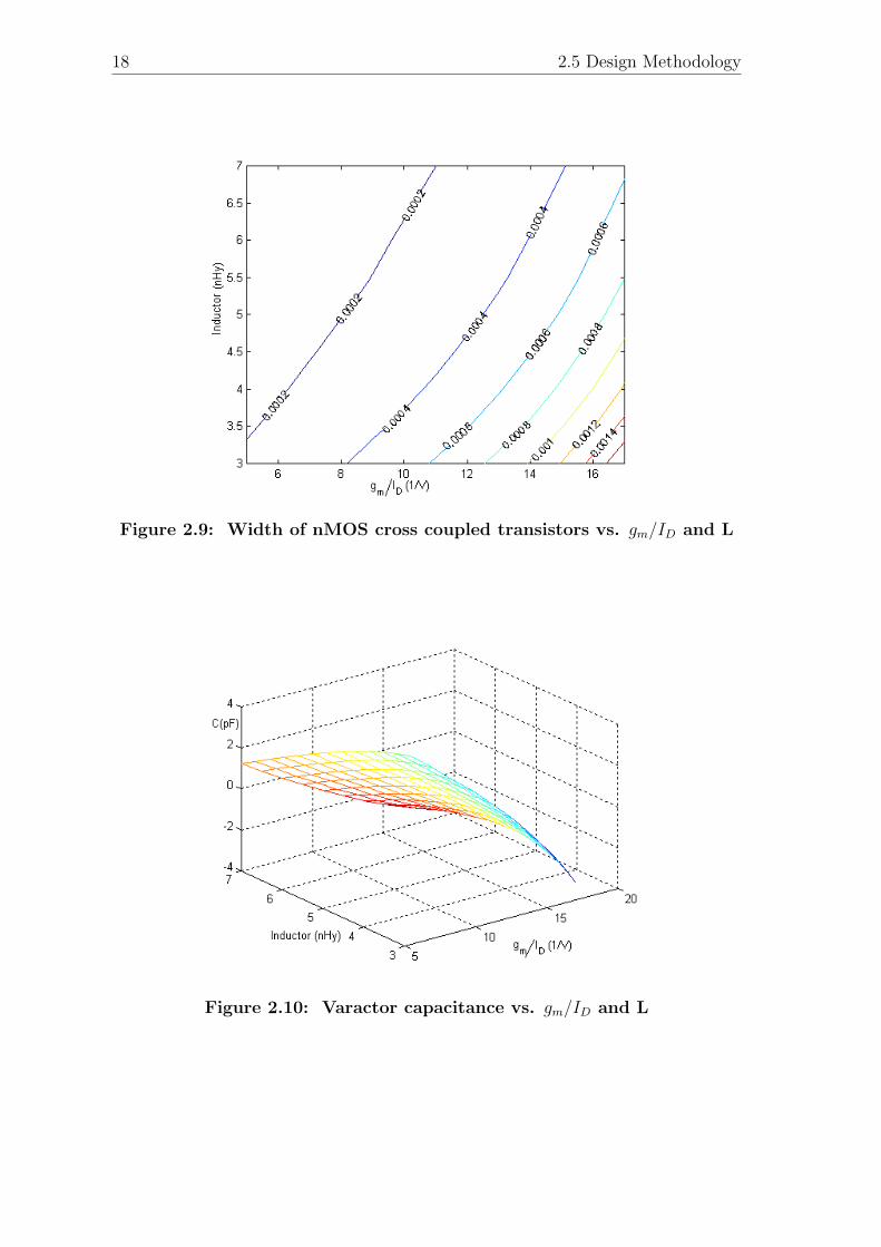
2.9 Width of nMOS cross coupled transistors vs. gm/ID and L . . . . . . . 18
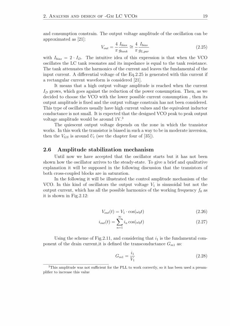
2.10 Varactor capacitance vs. gm/ID and L . . . . . . . . . . . . . . . . . . . 18
2.11 Amplitude stabilization mechanism in a -Gm block . . . . . . . . . . . . 20
2.12 Drain current of the VCO cross-coupled transistors vs. time . . . . . . . 20
2.13 Drain current of the cross-coupled transistors and varactor capacitanceversus gm/ID and inductor value L . . . . . . . . . . . . . . . . . . . . . 27
2.14 Multi-fingered layout of a transistor with width W . . . . . . . . . . . . 28
2.15 Floorplan of the cross-coupled complementary -Gm LC VCO . . . . . . 28
2.16 Separate transistor layout and interlaced layout of the pMOS cross-coupled block . . . . . . . . . . . . . . . . . . . . . . . . . . . . . . . . 29
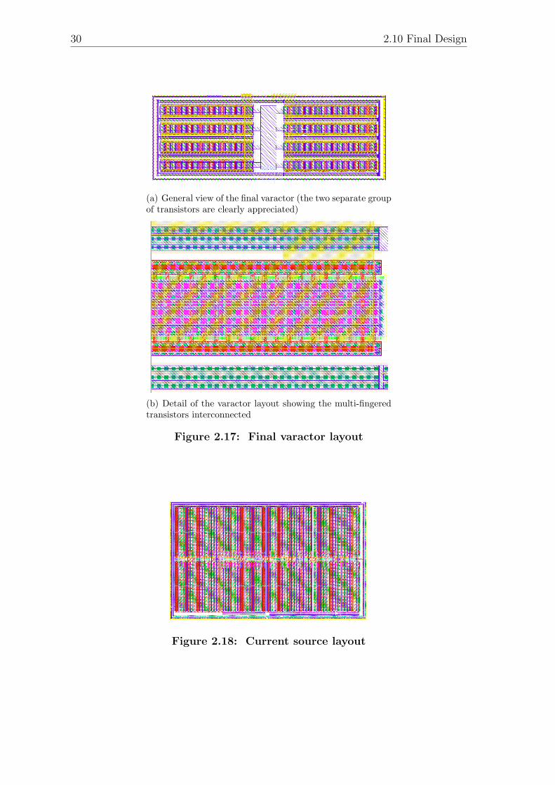
2.17 Final varactor layout . . . . . . . . . . . . . . . . . . . . . . . . . . . . 30
2.18 Current source layout . . . . . . . . . . . . . . . . . . . . . . . . . . . . 30
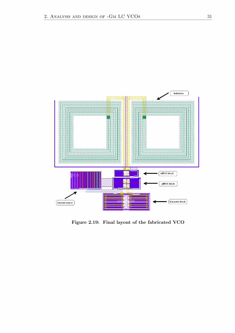
2.19 Final layout of the fabricated VCO . . . . . . . . . . . . . . . . . . . . 31
3.1 Signal spectrum and SSB power . . . . . . . . . . . . . . . . . . . . . . 34
3.2 RLC oscillator . . . . . . . . . . . . . . . . . . . . . . . . . . . . . . . . 35
3.3 Equivalent tank impedance value. . . . . . . . . . . . . . . . . . . . . . 35
3.4 Asymptotic graphic of Phase Noise. . . . . . . . . . . . . . . . . . . . . 37
vi
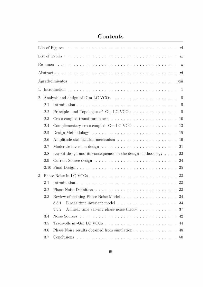
3.5 Impulse responses of LC tank . . . . . . . . . . . . . . . . . . . . . . . 38
3.6 Block diagram of the process . . . . . . . . . . . . . . . . . . . . . . . . 40
3.7 Evolution of circuit noise into phase noise . . . . . . . . . . . . . . . . . 41
3.8 Differential and complementary VCO . . . . . . . . . . . . . . . . . . . 42
3.9 Noise sources in a complementary differential LC-VCO oscillator. . . . . 43
3.10 Phase noise versus parallel tank resistance @ 600kHz from the carrier,considering a constant L. . . . . . . . . . . . . . . . . . . . . . . . . . . 46
3.11 Phase noise versus Inductance @ 600kHz from the carrier, consideringa constant Q. . . . . . . . . . . . . . . . . . . . . . . . . . . . . . . . . 46
3.12 Phase noise versus inductor quality factor Q @ 600kHz from the carrier,with a fixed L. . . . . . . . . . . . . . . . . . . . . . . . . . . . . . . . . 47
3.13 Figure of Merit (defined in 3.38) versus Q, Rs and Rpar. . . . . . . . . . 49
3.14 Figure of Merit versus gm/ID. . . . . . . . . . . . . . . . . . . . . . . . 50
3.15 Phase Noise vs. Inductance @600kHz offset from carrier for several gm/Id. 51
3.16 Phase noise versus the offset frequency calculated with Matlab for thedesigned VCO, for the LTI and LTV models. . . . . . . . . . . . . . . . 51
3.17 Simulated Phase Noise in Cadence. . . . . . . . . . . . . . . . . . . . . 52
4.1 Types of inductors’ layout. . . . . . . . . . . . . . . . . . . . . . . . . . 55
4.2 π net . . . . . . . . . . . . . . . . . . . . . . . . . . . . . . . . . . . . . 56
4.3 Monolithic inductor cross section view . . . . . . . . . . . . . . . . . . . 56
4.4 Inductor physical parameters . . . . . . . . . . . . . . . . . . . . . . . . 57
4.5 Eddy currents . . . . . . . . . . . . . . . . . . . . . . . . . . . . . . . . 59
4.6 Generation of substrate current on planar inductors . . . . . . . . . . . 60
4.7 Individual series resistance per metal trace . . . . . . . . . . . . . . . . 60
4.8 Conversion of the configuration of Rsi,Csi and Cox into a scheme of acapacitor Csi,ox and a resistance Rsi,ox in parallel. . . . . . . . . . . . . 61
4.9 π-model used in the ASITIC program. . . . . . . . . . . . . . . . . . . . 62
4.10 Scheme of the technology’s layers . . . . . . . . . . . . . . . . . . . . . 64
vii
4.11 Technology data given to the RF inductor’s modeler . . . . . . . . . . . 64
4.12 Final layout design of the inductor . . . . . . . . . . . . . . . . . . . . . 65
5.1 Used symbol of the p-n varactor and its simplified model. . . . . . . . 70
5.2 Typical structures of p-n reverse bias diode . . . . . . . . . . . . . . . . 70
5.3 Capacitance per unit area C′
gb versus VGB . . . . . . . . . . . . . . . . . 71
5.4 Transistor MOS seen as a three terminal structure . . . . . . . . . . . . 72
5.5 Characteristics of the D-S-B structure . . . . . . . . . . . . . . . . . . . 73
5.6 Inversion-mode MOS. . . . . . . . . . . . . . . . . . . . . . . . . . . . . 74
5.7 Accumulation-mode MOS. . . . . . . . . . . . . . . . . . . . . . . . . . 75
5.8 Differential structure of two I-MOS varactors. . . . . . . . . . . . . . . . 76
5.9 Inversion-mode varactor small-signal electrical model. . . . . . . . . . . 77
5.10 Simulated cgg curve of both varactors. . . . . . . . . . . . . . . . . . . . 78
5.11 Varactor Layout . . . . . . . . . . . . . . . . . . . . . . . . . . . . . . . 80
6.1 Structure of the buffer used . . . . . . . . . . . . . . . . . . . . . . . . . 82
6.2 Scheme of the buffer and its load (AC and DC load) as it is implementedin the PCB . . . . . . . . . . . . . . . . . . . . . . . . . . . . . . . . . . 82
6.3 Measurement setup for PSD tests and Phase Noise tests . . . . . . . . . 83
6.4 VCO oscillation frequency versus Vbias . . . . . . . . . . . . . . . . . . . 84
6.5 Die-photograph containing the PLL and the isolated VCO . . . . . . . . 85
6.6 VCO oscillation frequency versus Vbias . . . . . . . . . . . . . . . . . . . 85
A.1 Equivalent tank impedance value . . . . . . . . . . . . . . . . . . . . . 91
A.2 Equivalence of parallel circuit and series circuit . . . . . . . . . . . . . . 93
A.3 Conversion of the configuration of Rsi,Csi and Cox into a scheme of acapacitor Csi, ox and a resistance Rsi,ox in parallel. . . . . . . . . . . . . 94
B.1 Comparison of phase noise performance of a all-nMOS and a differentialLC VCO . . . . . . . . . . . . . . . . . . . . . . . . . . . . . . . . . . . 97
C.1 Layout of the PCB . . . . . . . . . . . . . . . . . . . . . . . . . . . . . 102
C.2 Final fabricated PCB . . . . . . . . . . . . . . . . . . . . . . . . . . . . 103
viii
List of Tables
1.1 Published works of LC voltage controlled oscillators’ design of the lastfew years . . . . . . . . . . . . . . . . . . . . . . . . . . . . . . . . . . . 2
2.1 Bias current of each cross-coupled transistors versus gm/ID and inductor L 21
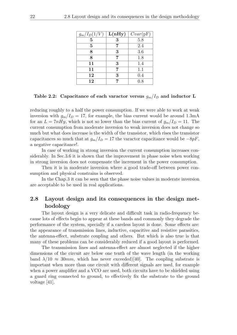
2.2 Capacitance of each varactor versus gm/ID and inductor L . . . . . . . 22
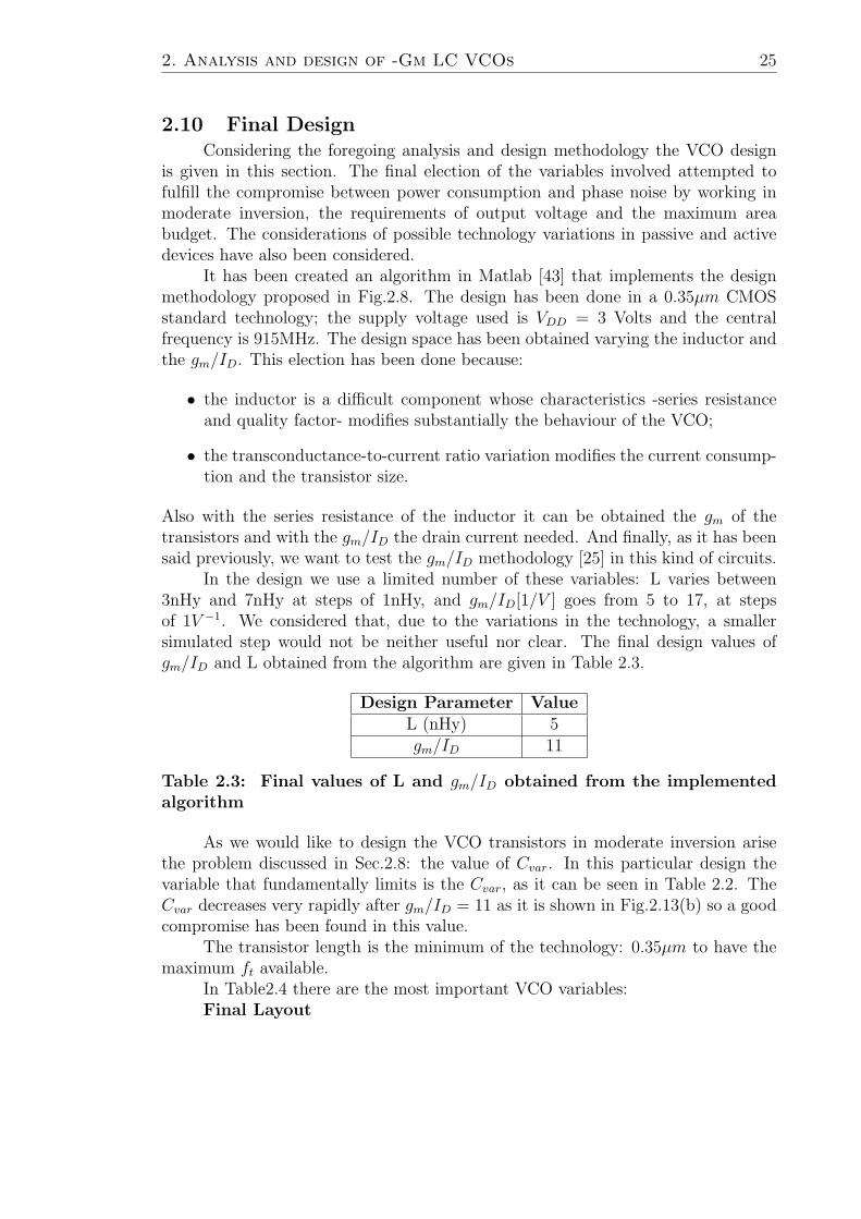
2.3 Final values of L and gm/ID obtained from the implemented algorithm . 25
2.4 Final values of several variables of the VCO design . . . . . . . . . . . . 26
4.1 Values of the constants K1 and K2 (defined in [1]) . . . . . . . . . . . . 58
4.2 Geometric parameters obtained with the function optarea of ASITIC . . 65
4.3 Parameters of the inductor calculated using the Yue’s Model and theMohan expressions. . . . . . . . . . . . . . . . . . . . . . . . . . . . . . 66
4.4 Parameters of the inductor calculated using ASITIC. . . . . . . . . . . 66
4.5 Parameters of the inductor calculated using RF Spectre Inductors’ Mo-deler. . . . . . . . . . . . . . . . . . . . . . . . . . . . . . . . . . . . . . 66
6.1 KV CO simulated and measured. . . . . . . . . . . . . . . . . . . . . . . 83
6.2 Phase noise measured at VDD = 3V and Ibias = 3mA . . . . . . . . . . . 84
ix
Resumen
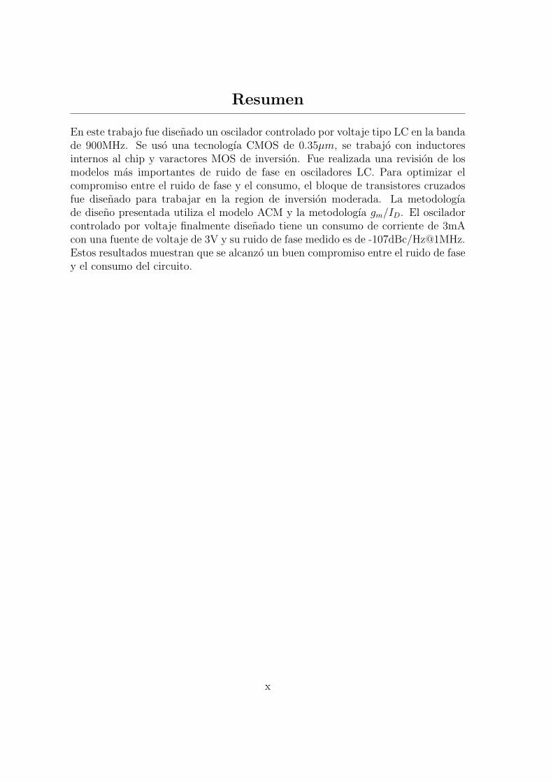
En este trabajo fue disenado un oscilador controlado por voltaje tipo LC en la bandade 900MHz. Se uso una tecnologıa CMOS de 0.35µm, se trabajo con inductoresinternos al chip y varactores MOS de inversion. Fue realizada una revision de losmodelos mas importantes de ruido de fase en osciladores LC. Para optimizar elcompromiso entre el ruido de fase y el consumo, el bloque de transistores cruzadosfue disenado para trabajar en la region de inversion moderada. La metodologıade diseno presentada utiliza el modelo ACM y la metodologıa gm/ID. El osciladorcontrolado por voltaje finalmente disenado tiene un consumo de corriente de 3mAcon una fuente de voltaje de 3V y su ruido de fase medido es de -107dBc/[email protected] resultados muestran que se alcanzo un buen compromiso entre el ruido de fasey el consumo del circuito.
x
Abstract
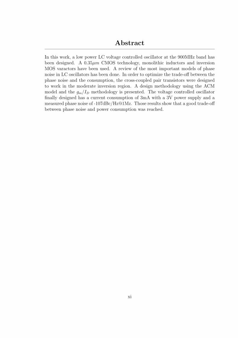
In this work, a low power LC voltage controlled oscillator at the 900MHz band hasbeen designed. A 0.35µm CMOS technology, monolithic inductors and inversionMOS varactors have been used. A review of the most important models of phasenoise in LC oscillators has been done. In order to optimize the trade-off between thephase noise and the consumption, the cross-coupled pair transistors were designedto work in the moderate inversion region. A design methodology using the ACMmodel and the gm/ID methodology is presented. The voltage controlled oscillatorfinally designed has a current consumption of 3mA with a 3V power supply and ameasured phase noise of -107dBc/Hz@1Mz. Those results show that a good trade-offbetween phase noise and power consumption was reached.
xi

xii
Agradecimientos
Me gustarıa expresar brevemente mi mas sincera gratitud a todas aquellas personasque, de una u otra forma, me apoyaron y ayudaron durante estos dos anos. Sin ellasno hubiese podido realizar satisfactoriamente este trabajo.
Primeramente, deseo agradecer a mi tutor, el Prof. Dr.Fernando Silveira, porsu invaluable guıa a lo largo de todo este trabajo. Las fructıferas discusiones ge-neradas y el apoyo brindado -tanto academico como humano- durante estos anosfueron indispensables para haber llevado esta tesis de maestrıa a buen puerto. Sin-ceramente, muchısimas gracias.
Por supuesto que quiero agradecer a las demas personas que integran el Grupode Microelectronica: MSc.Pablo Aguirre, MSc.Leonardo Barboni, Ing.Pablo Maz-zara, Ing.Linder Reyes e Ing.Conrado Rossi. Son muchısimos los momentos quenecesite de su ayuda y siempre la obtuve.
Deseo agradecer tambien a todas las personas que trabajan el en IIE. Paralos profesores, investigadores y personal no docente y para las secretarias (y suschocolates), muchısimas gracias por hacer posible que algunos de nosotros podamosrealizar posgrados en Uruguay.
Me gustarıa agradecer a la Facultad de Ingenierıa en su conjunto por habermeotorgado la beca de maestrıa. Tambien agradezco a CSIC por haber apoyado finan-cieramente mi pasantıa en Belgica.
Deseo expresar mi sincera gratitud a los integrantes del Laboratorio de Cir-cuitos Integrados DICE de la Universite catolique de Louvain la Neuve, en Belgica,muy especialmente al Dr. Denis Flandre por permitirme trabajar durante tres mesesen su laboratorio y a Laurent Vancaille y Bertrand Parvais entre muchos otros, porhaber sido tan hospitalarios durante mi estadıa en Belgica.
Deseo agradecer al Prof. Dr. Silva Martinez y a Alberto Valdes-Garcıa dela Universidad Texas A&M de Estados Unidos por habernos brindado informacionmuy valiosa sobre software de simulacion de inductores, tan necesario para estetrabajo.
Agradezco a la institucion MOSIS a traves de su programa MEP, por habernospermitido realizar chips de prueba al comienzo de esta maestrıa.
Mi pasantıa en Belgica no hubiese sido tan interesante y enriquecedora si nohubiese tenido en gusto de conocer a dos personas tan especiales como son GonzaloPicun y Silvia Rojas. Nunca sabre como pagarles por todo lo que hicieron por mıen esos meses. Muchas gracias.
Quiero agradecer de corazon a mis amigos. Siempre me han alentado a seguiradelante y se han interesado en lo que hago a pesar que aun no he sido capaz deexplicarles claramente que he estado estudiando. Quiero nombrar especialmente ados personas. A Denise Dalva por haberme acompanado incondicionalmente duranteestos anos. A Claudia Fumero, porque somos tan diferentes y tan iguales.
xiii
A mi novio Alfredo Arnaud. Alfre, tengo la gran suerte que tu, mi amor,entiendas lo que yo estudio. Te doy gracias por las infinitas horas del tiempo queme brindaste y que tanto me ayudaron. Te agradezco por haber estado junto a mitodos estos anos. Definitivamente no hubiese llegado hasta aquı sin ti.
Quiero agradecer por ultimo a mi familia: a mis adorados padres, Adrianay Reynaldo y al mas genial de los hermanos, Enzo. Ellos me han dado la fuerzay el carino que necesite para llegar hasta aquı. Tambien agradezco a Florencia,la hermana que me regalaron de grande y a Chiche, la abuela que me regalaronde grande. A mis abuelos, porque sin ellos no estarıa aquı y a Teco y Neca missegundos padres.
Le dedico este trabajo a dos personas que no estan aquı hoy pero que estoysegura estarıan felices de ver hasta donde he llegado. A mi querida Maestra Elena,y a Valentın.
xiv
Chapter 1Introduction
The explosive growth in radio-frequency applications has resulted in an in-creasing demand of wireless devices such as transceivers, receivers and transmitters[2] [3] [4] [5] [6] [7] [8] [9] [10]. The applications where these devices are used areuncountable. They go from short to long range communications systems and fromvery low to very high bit rates (such as local area networks). Depending on theapplication is the requirements of the power consumption of the system; for exam-ple, for short range and low bit rate communications the power consumption mightbe low. Sometimes the application fixes the voltage source needed; if the devicesmust use battery power supply and must have autonomy of several years its powerconsumption must be of few microwatts. If the system can be supplied by the mainsnetwork the power consumption can be of the order of miliwatts or even more. Fromthe previous discussion it is clear that the system requirements such as autonomy,range of communication or bit rates strongly condition the device design.
The work presented in this document is part of a design of a transmitterworking in the band of 900MHz. It is intended that this transmitter works undermost of the specifications of the IEEE 802.15.4 norm [11], whose applications aredirected to very low power consumption and very low data bit-rates. These devicesare usually attached to sensors of temperature, humidity, pressure, acceleration,chemical products among many others. They can log data coming from the sensorsor from an external data source. They can be used in agronomy (as reporting thesoil conditions or tracing the cattle), in cars (sending tires’ pressure or the state ofthe brakes), in industry (monitoring the temperature or the humidity of a controlledprocess of difficult or almost impossible access ) and even at home.
One of the most important blocks of the transmitter is the phase locked loop(PLL) which fixes the channel frequency. A PLL is a system with a feedback loopwhere an oscillator is controlled in such a way that its output signal has same phasethat the reference input signal. Its key block to obtain a good PLL performanceis the Voltage Controlled Oscillator (VCO). This block has an internal device thatmodifies its characteristics with a change in an input voltage Vbias. When Vbias
changes the VCO frequency oscillation is modified. The VCO features determinethe good quality of the PLL obtained. The VCO studied for this thesis was part of aPLL, which is under test. It has been used a LC VCO (L represents the inductanceand C the capacitance of the VCO ). It was designed in a 0.35µm standard CMOSdigital technology. The oscillation is produced at the frequency at which L and Cresonate. All the components of the VCO are on-chip, which means that it hasmonolithic inductors. We obtained a compact design with no need of external chipcomponents. However, the standard CMOS technology used constrains the qualityfactor of the inductor obtained, which jeopardizes the performance of the VCO
1
2
Referen
ceTech
nology
Freq
Phase
Noise
Tunin
gR
ange
Con
sum
ption
Inductors
Varactors
[12]0.5
µm
CM
OS
434MH
z-111dB
c/Hz
@600kH
z1.6%
0.23mA
off-chipaccum
ulation-mode
[13]0.6
µm
CM
OS
2.4GH
z-118dB
c/Hz
@1M
Hz
11%9m
Aon-chip
inversion-mode
[14]0.25µ
mC
MO
S4G
Hz
-117dBc/H
z@
1MH
z15%
3mA
on-chipnew
structure[15]
0.7µm
CM
OS
1.8GH
z-116dB
c/Hz
@600kH
z13%
4mA
on-chip?
[16]0.35µ
mC
MO
S2.4G
Hz
-105dBc/H
z@
100kHz
14%4.5m
Aon-chip
accumulation-m
ode[17]
0.18µm
CM
OS
5.3GH
z-124dB
c/Hz
@1M
Hz
10%7.5m
Aon-chip
p+/n-w
elldiodes
[18]0.65
µm
BiC
MO
S2G
Hz
-125dBc/H
z@
600kHz
11%19m
Aon-chip
p+/n-w
elldiodes
[19]0.35µ
mC
MO
S1.3G
Hz
-119dBc/H
z@
600kHz
28%6m
Aon-chip
andbond-w
ireaccum
ulation-mode
[20]0.35
µm
BiC
MO
S2G
Hz
-117dBc/H
z@
600kHz
26%4m
Aon-chip
?[21]
0.25µ
mC
MO
S1.8G
Hz
-121dBc/H
z@
600kHz
?2m
Aon-chip
?
Table
1.1
:P
ublish
ed
work
sofLC
volta
ge
contro
lled
oscilla
tors’
desig
nofth
ela
stfe
wyears
1. Introduction 3
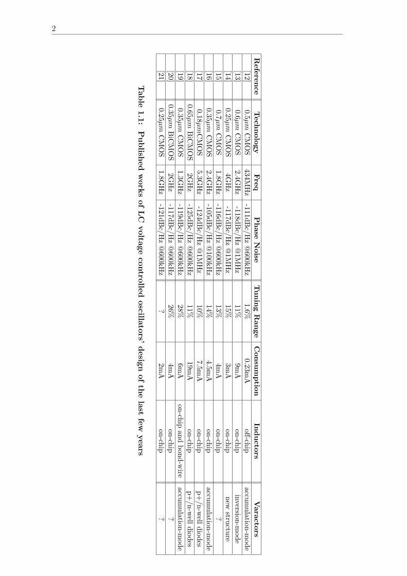
[22][23][24].This kind of VCOs has been widely studied in the last years, and several
publications have shown very interesting results on this matter. To show the state-of-the-art of this subject, it is given a summary of the most important works inTable 1.1. The benchmarks used to compare these works are: the phase noise rea-ched at a certain frequency, the tuning range of the VCO, the current consumptionand construction of the inductor on-chip or off-chip. The results depend also on thetechnology used, the working frequency and the kind of varactors implemented. Inthis summary the range of frequency given goes from 433MHz to 5.3GHz. We focu-sed particularly on designing a VCO with the lowest possible current consumptionwithout increasing too much the phase noise.
To design the VCO transistors the gm/ID methodology [25] was utilized . Thisunifies the treatment of all regions of operation, and with this it is obtained a relationbetween gm/ID and the normalized current ID/(W/L). It is found that the gm/IDcurve is a common characteristic of all the transistors belonging to a same process.
The ACM model [26] has been the transistor model used to do the analyticalcomputations. This physically based model describes all the operation regions withcontinuous, simple and accurate expressions. This kind of model was a necessity inour work as we were interested in studing the VCO transistors in all the operationregions, specially in the moderate inversion region. Combining the ACM model andthe gm/ID methodology it is very easy to compute the transistor dimensions.The VCO initial specifications were the following:
• the technology must be a CMOS standard technology.
• the VCO will be used in a very low power consumption system so it must havea power consumption as low as possible.
• the supply voltage will be 3V but can drop to 2.4V (if two batteries of 1.2Vare used).
• the phase noise of the PLL depends strongly on the phase noise of the VCO,so an acceptable value of the last one must be reached to fulfill as much aspossible the IEEE802.15.4[11] requirements.
• the occupied area of the VCO is limited to 600µm by 600µm -it has been anarbitrary chosen value-.
• the tuning range must be at least 3.2%, because the band of 915MHz of theIEEE802.15.4[11] is 15MHz around 915MHz.
• it has to handle a load capacitance (coming from the other blocks of the PLL)of 0.6pF on each output port.
The summary of the contents of this work is as follows:
4
Chapter 2: Analysis and design of -Gm LC VCOs In this chapter is studiedthe type of VCOs used. Various architectures are presented and it is discussedwhy the used topology is chosen. Also it is studied the mechanism of oscillationof these devices. The design methodology proposed in this work and the choiceof transistors working in moderate inversion region is explained. Finally, adiscussion on the design of the layout is given.
Chapter 3: Phase Noise in LC VCOs The phase noise is a fundamental cha-racteristic of the VCO. Two models -an empirical and a physical-based model-are described, showing the advantages of each one of them. The noise sourcesand the phase noise expressions of the topology used are given. A discussionof the trade-offs between the phase noise and the power consumption is pre-sented. Finally, the values of the phase noise (calculated and simulated) areshown.
Chapter 4: Inductors Design In this chapter several types of monolithic induc-tors are shown as well as some models to calculate its physical characteristics.The simulation tools used during this work are proposed. Finally, the inductordesign methodology is described and the parameters of the final inductor usedare shown.
Chapter 5: Varactor Design In this chapter the most common topologies of va-ractors are presented and, specifically, the varactor topology used in this workis deeply studied. At the end, the final varactor characteristics are shown.
Chapter 6: Measurements In this chapter the measurement setup is presentedas well as the measured results.
Chapter 7: Conclusions and Future Work
Chapter 2Analysis and design of -Gm LC VCOs
2.1 IntroductionThe voltage controlled oscillators (VCO) designed in CMOS technologies have
become nowadays a real solution in the band of radio frequencies (from now on RF)because of having achieved low power consumption and low phase noise values.
Also the use of on-chip inductors is now acceptable in RF [15] [19] [18] [27]. In the band of 900MHz it has been also possible to design and use monolithicinductors despite its size [28]. In this frequency the size of the inductor increasesbecause in an LC oscillator the oscillation frequency ω0 is:
ω20 =
1
LC(2.1)
and if the frequency ω0 decreases and the capacitor value is maintained constantthe inductor value must increase.
In this chapter the principles and equations that governs the Gm LC VCO typewill be studied. Various of its topologies are reviewed, putting particular attentionin the complementary cross-coupled -Gm LC VCO, which is the one used throughoutthis work.
Also a VCO design methodology is presented using the equations that deter-mine the VCO oscillation and the ACM CMOS transistor model [26]. This metho-dology is based on finding good trade-offs between power consumption and phasenoise.
Another aim of this chapter is to show that at 900MHz the cross-coupledtransistor block can work correctly in moderate inversion and that at this level ofinversion the power consumption is improved without jeopardizing other characte-ristics of the VCO.
Finally the complete set of design parameters of the utilized VCO are presen-ted.
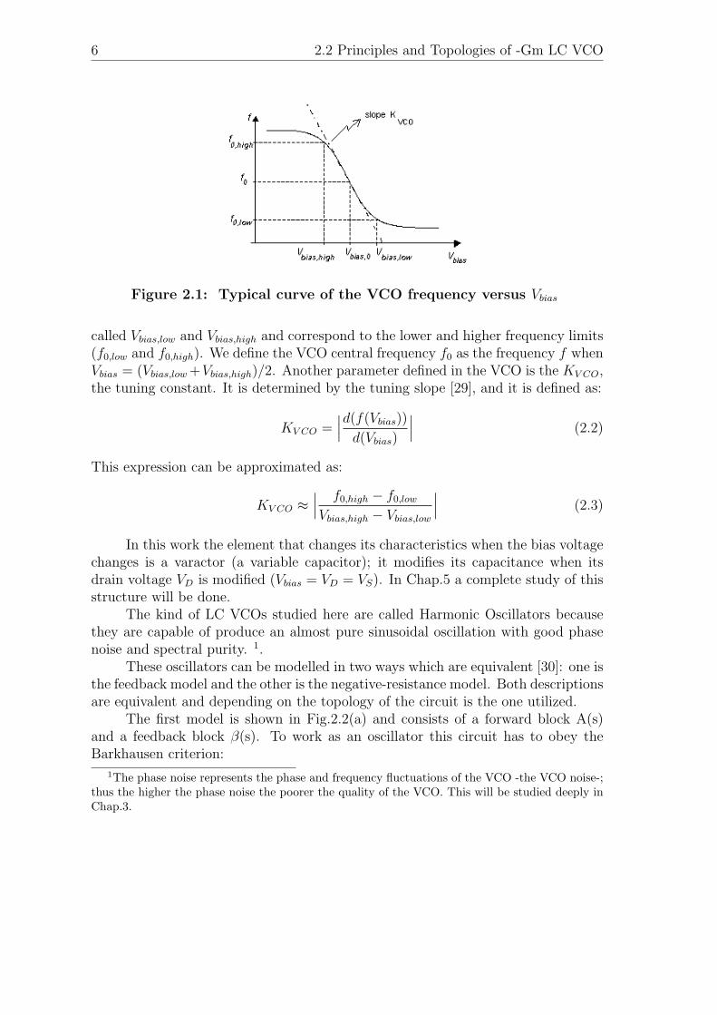
2.2 Principles and Topologies of -Gm LC VCOA VCO is an oscillator whose oscillation frequency -or working frequency- can
be modified using an external bias voltage Vbias. It is very important the way thefrequency of the VCO f varies when Vbias changes. If the curve f vs Vbias is asshown in Fig.2.1, some characteristics of the VCO can be defined. Firstly, there is acentral zone of the curve where the frequency varies linearly with Vbias as shown withthe straight line of Fig.2.1. The limits of the linearized zone are where the straightline begins to separate from the curve. The voltages where these limits occur are
5
6 2.2 Principles and Topologies of -Gm LC VCO
Figure 2.1: Typical curve of the VCO frequency versus Vbias
called Vbias,low and Vbias,high and correspond to the lower and higher frequency limits(f0,low and f0,high). We define the VCO central frequency f0 as the frequency f whenVbias = (Vbias,low +Vbias,high)/2. Another parameter defined in the VCO is the KV CO,the tuning constant. It is determined by the tuning slope [29], and it is defined as:
KV CO =∣∣∣d(f(Vbias))
d(Vbias)
∣∣∣ (2.2)
This expression can be approximated as:
KV CO ≈∣∣∣ f0,high − f0,low
Vbias,high − Vbias,low
∣∣∣ (2.3)
In this work the element that changes its characteristics when the bias voltagechanges is a varactor (a variable capacitor); it modifies its capacitance when itsdrain voltage VD is modified (Vbias = VD = VS). In Chap.5 a complete study of thisstructure will be done.
The kind of LC VCOs studied here are called Harmonic Oscillators becausethey are capable of produce an almost pure sinusoidal oscillation with good phasenoise and spectral purity. 1.
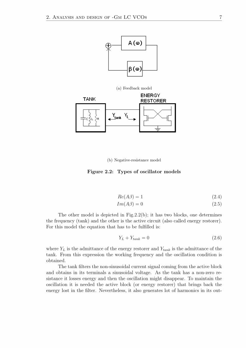
These oscillators can be modelled in two ways which are equivalent [30]: one isthe feedback model and the other is the negative-resistance model. Both descriptionsare equivalent and depending on the topology of the circuit is the one utilized.
The first model is shown in Fig.2.2(a) and consists of a forward block A(s)and a feedback block β(s). To work as an oscillator this circuit has to obey theBarkhausen criterion:
1The phase noise represents the phase and frequency fluctuations of the VCO -the VCO noise-;thus the higher the phase noise the poorer the quality of the VCO. This will be studied deeply inChap.3.
2. Analysis and design of -Gm LC VCOs 7
(a) Feedback model
(b) Negative-resistance model
Figure 2.2: Types of oscillator models
Re(Aβ) = 1 (2.4)
Im(Aβ) = 0 (2.5)
The other model is depicted in Fig.2.2(b); it has two blocks, one determinesthe frequency (tank) and the other is the active circuit (also called energy restorer).For this model the equation that has to be fulfilled is:
YL + Ytank = 0 (2.6)
where YL is the admittance of the energy restorer and Ytank is the admittance of thetank. From this expression the working frequency and the oscillation condition isobtained.
The tank filters the non-sinusoidal current signal coming from the active blockand obtains in its terminals a sinusoidal voltage. As the tank has a non-zero re-sistance it losses energy and then the oscillation might disappear. To maintain theoscillation it is needed the active block (or energy restorer) that brings back theenergy lost in the filter. Nevertheless, it also generates lot of harmonics in its out-
8 2.2 Principles and Topologies of -Gm LC VCO
put current, which are filtered in the tank. This model is called negative-resistancemodel because the energy restorer can be seen as a negative resistance that com-pensates the parasitic resistance of the tank.
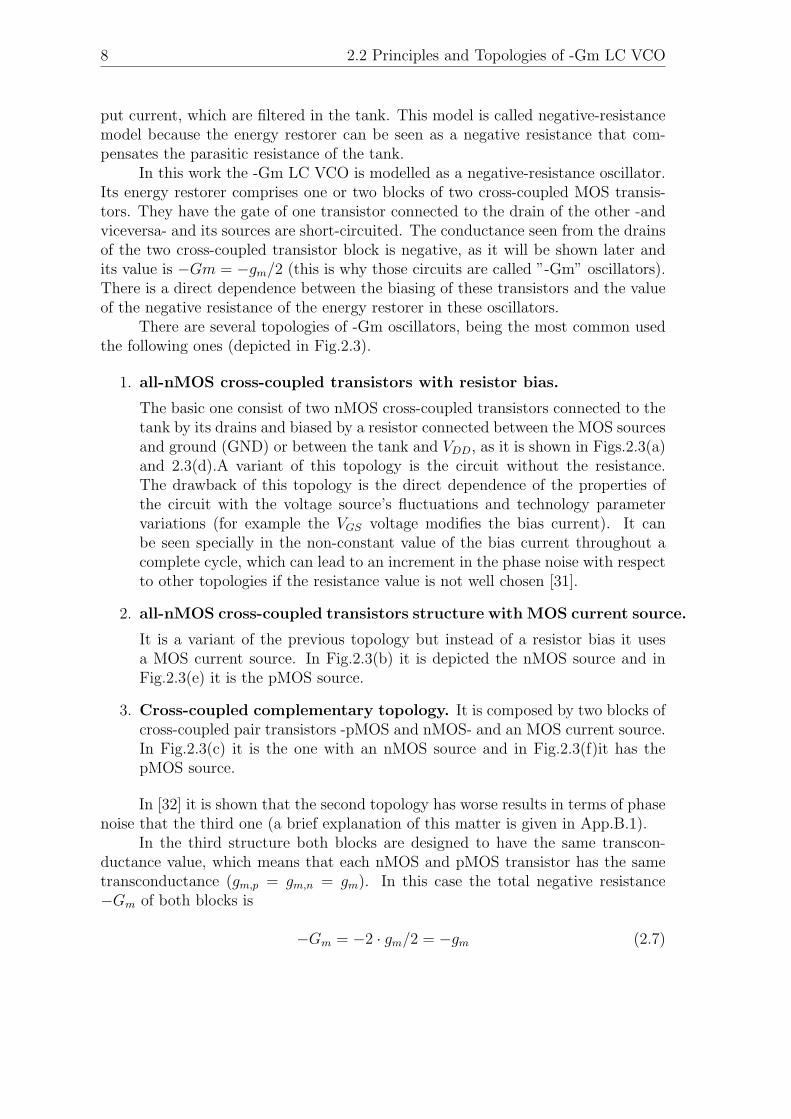
In this work the -Gm LC VCO is modelled as a negative-resistance oscillator.Its energy restorer comprises one or two blocks of two cross-coupled MOS transis-tors. They have the gate of one transistor connected to the drain of the other -andviceversa- and its sources are short-circuited. The conductance seen from the drainsof the two cross-coupled transistor block is negative, as it will be shown later andits value is −Gm = −gm/2 (this is why those circuits are called ”-Gm” oscillators).There is a direct dependence between the biasing of these transistors and the valueof the negative resistance of the energy restorer in these oscillators.
There are several topologies of -Gm oscillators, being the most common usedthe following ones (depicted in Fig.2.3).
1. all-nMOS cross-coupled transistors with resistor bias.
The basic one consist of two nMOS cross-coupled transistors connected to thetank by its drains and biased by a resistor connected between the MOS sourcesand ground (GND) or between the tank and VDD, as it is shown in Figs.2.3(a)and 2.3(d).A variant of this topology is the circuit without the resistance.The drawback of this topology is the direct dependence of the properties ofthe circuit with the voltage source’s fluctuations and technology parametervariations (for example the VGS voltage modifies the bias current). It canbe seen specially in the non-constant value of the bias current throughout acomplete cycle, which can lead to an increment in the phase noise with respectto other topologies if the resistance value is not well chosen [31].
2. all-nMOS cross-coupled transistors structure with MOS current source.
It is a variant of the previous topology but instead of a resistor bias it usesa MOS current source. In Fig.2.3(b) it is depicted the nMOS source and inFig.2.3(e) it is the pMOS source.
3. Cross-coupled complementary topology. It is composed by two blocks ofcross-coupled pair transistors -pMOS and nMOS- and an MOS current source.In Fig.2.3(c) it is the one with an nMOS source and in Fig.2.3(f)it has thepMOS source.
In [32] it is shown that the second topology has worse results in terms of phasenoise that the third one (a brief explanation of this matter is given in App.B.1).
In the third structure both blocks are designed to have the same transcon-ductance value, which means that each nMOS and pMOS transistor has the sametransconductance (gm,p = gm,n = gm). In this case the total negative resistance−Gm of both blocks is
−Gm = −2 · gm/2 = −gm (2.7)
2. Analysis and design of -Gm LC VCOs 9
(a) Cross-coupled (resistor bia-sed)
(b) Cross-coupled (n-TypeMOS current source)
(c) Cross-coupled complemen-tary (n-Type current source)
(d) Cross-coupled (resistor bia-sed)
(e) Cross-coupled (p-TypeMOS current source)
(f) Cross-coupled complemen-tary (p-Type MOS currentsource)
Figure 2.3: Different topologies of -Gm LC VCO
10 2.3 Cross-coupled transistors block
However, the addition of two more transistors -specially the p-MOS ones-raises the value of the parasitic capacitance which might be a problem in the design.Also this topology cannot scale down to lower the supply voltage compared with theall-nMOS cross-coupled topology because it uses an extra Vgs. On the other handas in the all-nMOS structure the dc value of the drain voltage is almost VDD, thedc voltage drop across the channel is larger than in the complementary VCO, whichcan lead to stronger velocity saturation [21].
A topology which has not been shown in Fig.2.3 is the one that uses a cross-coupled p-MOS transistor block instead of a n-MOS one. As it is studied in [17]the all-pMOS topology with pMOS current source has a little better performancerespect of the all-nMOS structure with nMOS current source.
The pMOS current source that is used in the second and third structures fixesthe bias current of the VCO independent of the supply voltage. As the currentsource adds phase noise to the VCO and the pMOS transistors have better flickernoise figures, in this work it has been used the pMOS transistors to build the thecurrent source.
In our design we have chosen the cross-coupled complementary topology ( seeFig.2.3(f)) to design our VCO.
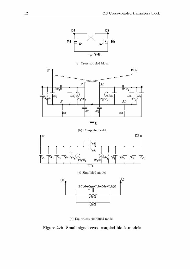
2.3 Cross-coupled transistors blockTo study the operation of the VCO it is needed to know how the cross coupled
transistors block works. To do that, we will study this block using the small-signalmodel for the transistors. In this study -as depicted in Fig.2.4(a), their commonsource has a constant voltage value because the circuit has a symmetrical structure(the transistors are considered identical) and the output voltage (the voltage betweenits drains) is differential. Then this point is considered virtual ground at small-signal.
The transistor model used is the quasi-static model five intrinsic capacitancemodel which considers the capacitances Cgd, Cgs, Cdb, Cgd, Cgb [33]. It has beenalso considered the capacitance Cds. In the used model there are not considered thechannel resistance, the gate intrinsic resistance and the transconductance delay [34][35]).2
The extrinsic capacitances are also considered in the study. In Fig.2.4(b) is thesmall-signal model of the block. The overlap and junction capacitances are includedtogether with the intrinsic ones, despite they are not explicitly mentioned in thescheme).
As bulk and source voltages are virtual ground, the capacitances Csb are short-circuited in the small-signal operation, being the resulting circuit the one shown inFig.2.4(c).
Since the transistors, their bias current and their capacitances are consideredidentical; and as the gate of one transistor is crossed with the drain of the other; a
2The designed nMOs transistors work below the quasi-static limit, the pMOS are a bit overthat limit.

2. Analysis and design of -Gm LC VCOs 11
simple differential model of the block can be obtained (see Fig.2.4(d)). The capaci-tance Cgd,1||Cgd,2 is split in two capacitances in series of value 2 · (Cgd,1||Cgd,2) andthe middle point can be considered as virtual ground. Then it is possible to have allthe capacitances of the circuit in parallel and to obtain the equivalent capacitanceseen by the drains of the transistors, whose value is:
Ceq,−Gm = 2Cgd +(Cgs + Cdb + Cds + Cgb)
2(2.8)
To explain the transformation of the transconductance of the transistors intoa negative resistance shown in Fig.2.4(d) lets take the transistor M1 of Fig.2.4(a).The gate-source voltage of M1 is the drain-source voltage of M2, then gm,1vgs,1 =gm,1vds,2. As vds,1 = −vds,2 (because of the differential output voltage) then gm,1vgs,1 =−gm,1vds,1. Not considering the capacitances and the conductance gds,−gm,1vds,1 isthe current going through vds,1, then −gm,1 can be seen as a negative resistancebetween drain and source.
Then the total equivalent conductance of this block is:
Geq = −gm
2+ gds (2.9)
Assuming that in the bias point the transistor is in the saturation region,gds gm and then:
Geq∼= −gm
2= −Gm (2.10)
Using the ACM transistor model [26], the expression of the Ceq,−Gm in satu-ration is:
Ceq,−Gm = 2·Cov,gd +Cov,gs + Cjd,db
2+
(n− 1)Cox +(
23Cox(
√1 + i− 1)
√1+i+2
(√
1+i+1)2
)2n
(2.11)where n is the slope factor [36], slightly dependent on the gate voltage, greater thanone and usually smaller than two. i is the normalized current [26]:
i ∼=IDIS
(2.12)
and
IS = µnCoxU2
t
2
W
L(2.13)
where µ is the carrier mobility, Cox is the oxide capacitance per unit area, Ut is thethermal voltage and W and L are the width and length of the transistors.
12 2.3 Cross-coupled transistors block
(a) Cross-coupled block
(b) Complete model
(c) Simplified model
(d) Equivalent simplified model
Figure 2.4: Small signal cross-coupled block models
2. Analysis and design of -Gm LC VCOs 13
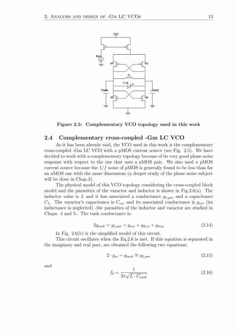
Figure 2.5: Complementary VCO topology used in this work
2.4 Complementary cross-coupled -Gm LC VCOAs it has been already said, the VCO used in this work is the complementary
cross-coupled -Gm LC VCO with a pMOS current source (see Fig. 2.5). We havedecided to work with a complementary topology because of its very good phase noiseresponse with respect to the one that uses a nMOS pair. We also used a pMOScurrent source because the 1/f noise of pMOS is generally found to be less than foran nMOS one with the same dimensions (a deeper study of the phase noise subjectwill be done in Chap.3).
The physical model of this VCO topology considering the cross-coupled blockmodel and the parasitics of the varactor and inductor is shown in Fig.2.6(a). Theinductor value is L and it has associated a conductance gL,par and a capacitanceCL. The varactor’s capacitance is Cvar and its associated conductance is gvar (itsinductance is neglected) -the parasitics of the inductor and varactor are studied inChaps. 4 and 5-. The tank conductance is:
2gtank = gL,par + gvar + gds,n + gds,p (2.14)
In Fig. 2.6(b) is the simplified model of this circuit.This circuit oscillates when the Eq.2.6 is met. If this equation is separated in
the imaginary and real part, are obtained the following two equations:
2 · gm = gtank∼= gL,par (2.15)
and
f0 =1
2π√L · Ctank
(2.16)
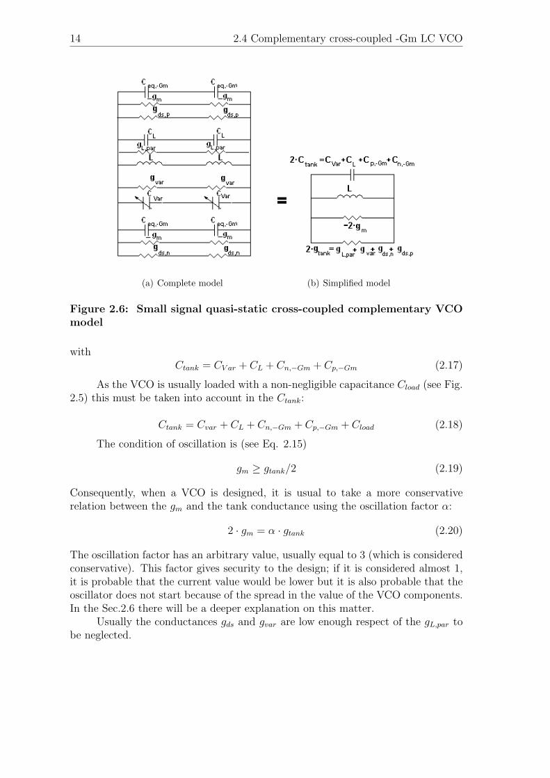
14 2.4 Complementary cross-coupled -Gm LC VCO
(a) Complete model (b) Simplified model
Figure 2.6: Small signal quasi-static cross-coupled complementary VCOmodel
withCtank = CV ar + CL + Cn,−Gm + Cp,−Gm (2.17)
As the VCO is usually loaded with a non-negligible capacitance Cload (see Fig.2.5) this must be taken into account in the Ctank:
Ctank = Cvar + CL + Cn,−Gm + Cp,−Gm + Cload (2.18)
The condition of oscillation is (see Eq. 2.15)
gm ≥ gtank/2 (2.19)
Consequently, when a VCO is designed, it is usual to take a more conservativerelation between the gm and the tank conductance using the oscillation factor α:
2 · gm = α · gtank (2.20)
The oscillation factor has an arbitrary value, usually equal to 3 (which is consideredconservative). This factor gives security to the design; if it is considered almost 1,it is probable that the current value would be lower but it is also probable that theoscillator does not start because of the spread in the value of the VCO components.In the Sec.2.6 there will be a deeper explanation on this matter.
Usually the conductances gds and gvar are low enough respect of the gL,par tobe neglected.
2. Analysis and design of -Gm LC VCOs 15
2.5 Design MethodologyThe design methodology presented here can be used in any of the VCO topo-
logies shown previously, but it is focused on particularly the cross-coupled comple-mentary -Gm LC VCO.
The specifications of the VCO are very related with the system in which it ispart. The VCO designed here will be part of a Phase Locked Loop (PLL), whosespecifications of power and phase noise are rigorous so that it can be used in com-munication circuits (as transmitters and receivers) which fulfill the IEEE 802.15.4standard. The VCO can modify substantially the phase noise or power consumptionvalues [37] of a PLL. Thus, one of the most important VCOs specifications are themaximum power consumption and the maximum phase noise (and sometimes theminimum peak output voltage).
As this VCO has on-chip inductors and these take substantial silicon area,the total VCO area is usually an important fraction of the total area of the systemin which it is embedded. For this reason, the maximum VCO total area is alsospecified. The on-chip inductors are strongly conditioned by this requirement.
The VCO physical parameters to be found in the design flow are: the induc-tance value and its parasitics, the varactor’s value and its characteristics, the sizeof the pMOS and nMOS transistors and the size of the bias current pMOS tran-sistors. It has to be considered the parasitics of the layout in the design -usuallycapacitances at the working frequencies- and the load capacitance Cload of the loadof the VCO.
One important design parameter used in this methodology is the transconductance-to-current ratio gm/ID [25]. This ratio can be expressed in terms of the normalizedcurrent i (Eq.2.12) [33]:
gm
ID=
2
nUt(√
1 + i+ 1)(2.21)
As i = ID/IS and IS ∝ W/L then
i = k · ID/(W/L) (2.22)
with
k =2
µnCoxU2t
(2.23)
It means that gm/ID can be plotted versus ID/(W/L). This curve is a charac-teristic curve that depends only on the technology. Particularly this characteristiccurve is very useful as it relates the transistor gm/ID with gm knowing the draincurrent ID (and viceversa); or relates the transistor aspect ratio W/L with gm kno-wing ID. Its typical behaviour is showed in Fig.2.7, where it is plotted the measuredcharacteristic curve of gm/ID of the nMOS transistor 0.35µm technology.
The technology used also determines the characteristics of:
• the inductance: its value L, the quality factor Q, the resistive losses RL,par.

16 2.5 Design Methodology
Figure 2.7: gm/ID measured and estimated for a L = 0.35µm,W = 200µmnMOS transistor (estimation calculated implementing the ACM model[33] in a Matlab routine, with n=1.25)
• the varactor: its capacitive curve, the VCO gain KV CO.
• the transistors: the parasitic capacitances and gm.
From Eq.2.15 and the assumption that gtank ≈ gL,par, gm = α·gL,par/2. Then, ifgm/ID of the transistorsMi,[i=1..4] is increased while α and the inductance electricalcharacteristics (L, gL,par,CL) are fixed, gm is set and ID decreases (with ID = Ibias/2).It leads to a reduction in the VCO power consumption. However, the minimumpossible value of ID is limited by the maximum oscillator phase noise value specified[38] [39], as it increases when ID drops (the Phase Noise behaviour will be studiedin Chap.3). It is also limited by the parasitic capacitances of the transistors Mi,i=1..4 (see Fig. 2.5), since an increment in gm/ID with gm constant produces anincrement in the transistor’s width[33]:
W = L · gm ·kgm/ID
4nUt
(1
nUt− gm/ID
) (2.24)
An increment in the transistor width W also restricts the oscillation frequencyand diminish the tuning range. It is because a higher W is equivalent to highertransistor parasitic capacitances -which reduces the possible varactor capacitance ormakes it negative-.
Considering the previous discussion, the proposed VCO design methodologyis presented in the scheme of Fig.2.8. Given an inductor value L and a oscillationfrequency f0, the inductor dimensions and its parameters are calculated (gL,par and

2. Analysis and design of -Gm LC VCOs 17
Figure 2.8: Design methodology
Q among others). With these parameters, gm/ID and α, it is found ID. Using thetransistor’s characteristic curves of Fig.2.7 or the Eq.2.21, the width of Mi’s areobtained. At last, the varactor capacitance Cvar is calculated. If the phase noise Lis higher than Lmax or the varactor capacitance Cvar is less than a Cvar,min then thegm/ID or the L chosen have to be changed.
With the previous discussion about the complementary VCO and the designmethodology several possible situations can be pointed out:
• Using Eq.2.24, if gm/ID is fixed, when the inductor value increases the transis-tor width W decreases (see Fig.2.9). The reason is that the rise of the inductoralso increases the inductor series resistance, decreasing gL,par and hence thegm of the transistors (see Eq.2.15).
• Also from Eq.2.24 for a fixed inductor, if gm/ID rises then W increases becausegm is constant. This behaviour is shown in Fig.2.9.
• Usually the inductor capacitance is higher than the transistor capacitances andthen if the inductor value grows, despite the transistor width falls, the varactorcapacitance decreases (remember that the total VCO capacitance must fulfillthe Eq. 2.16) (see Fig.2.10, Cvar versus L).
• For a constant inductor value, the gm is constant and if gm/ID increases, fromEq.2.24, the W increases and the varactor capacitance decreases. The totalcapacitance of the VCO can be so high that Cvar would fall below zero ( seein Fig.2.10 the plot of Cvar versus gm/ID)
The VCO output voltage is a specification which has been taken into conside-ration in the methodology design but it has had less influence that the phase noise
18 2.5 Design Methodology
Figure 2.9: Width of nMOS cross coupled transistors vs. gm/ID and L
Figure 2.10: Varactor capacitance vs. gm/ID and L
2. Analysis and design of -Gm LC VCOs 19
and consumption constrain. The output voltage amplitude of the oscillation can beapproximated as [21]:
Vout =4
π
Ibias
gtank
∼=4
π
Ibias
gL,par
(2.25)
with Ibias = 2 · ID. The intuitive idea of this expression is that when the VCOoscillates the LC tank resonates and its impedance is equal to the tank resistance.The tank attenuates the harmonics of the current and leaves the fundamental of theinput current. A differential voltage of the Eq.2.25 is generated with this current ifa rectangular current waveform is considered [21].
It means that a high output voltage amplitude is reached when the currentID grows, which goes against the reduction of the power consumption. Then, as wedecided to choose the VCO with the lower possible current consumption , then itsoutput amplitude is fixed and the output voltage constrain has not been considered.This type of oscillators usually have high current values and the equivalent inductorconductance is not small. It is expected that the designed VCO peak to peak outputvoltage amplitude would be around 1V.3
The quiescent output voltage depends on the zone in which the transistorworks. In this work the transistor is biased in such a way to be in moderate inversion,then the VGS is around Ut (see the chapter four of [35]).
2.6 Amplitude stabilization mechanismUntil now we have accepted that the oscillator starts but it has not been
shown how the oscillator arrives to the steady-state. To give a brief and qualitativeexplanation it will be supposed in the following discussion that the transistors ofboth cross-coupled blocks are in saturation.
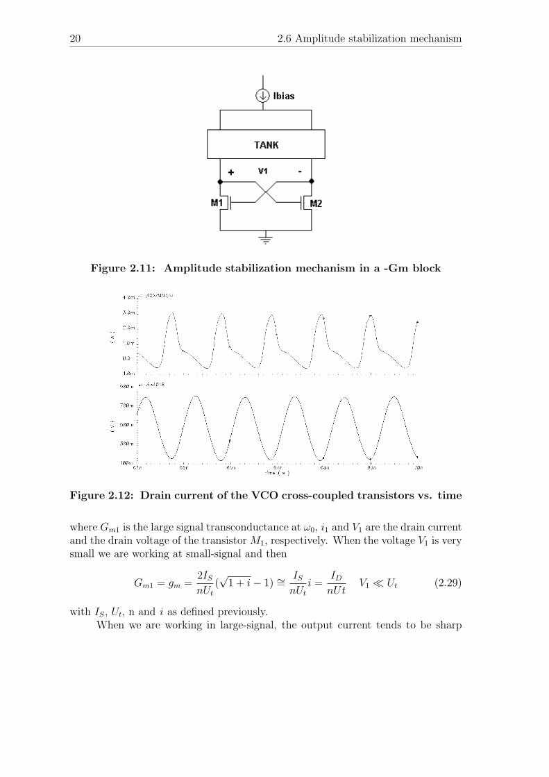
In the following it will be illustrated the control amplitude mechanism of theVCO. In this kind of oscillators the output voltage V1 is sinusoidal but not theoutput current, which has all the possible harmonics of the working frequency f0 asit is shown in Fig.2.12:
Vout(t) = V1 · cos(ω0t) (2.26)
iout(t) =∞∑
n=1
in cos(ω0t) (2.27)
Using the scheme of Fig.2.11, and considering that i1 is the fundamental com-ponent of the drain current,it is defined the transconductance Gm1 as:
Gm1 =i1V1
(2.28)
3This amplitude was not sufficient for the PLL to work correctly, so it has been used a pream-plifier to increase this value
20 2.6 Amplitude stabilization mechanism
Figure 2.11: Amplitude stabilization mechanism in a -Gm block
Figure 2.12: Drain current of the VCO cross-coupled transistors vs. time
where Gm1 is the large signal transconductance at ω0, i1 and V1 are the drain currentand the drain voltage of the transistor M1, respectively. When the voltage V1 is verysmall we are working at small-signal and then
Gm1 = gm =2ISnUt
(√
1 + i− 1) ∼=ISnUt
i =IDnUt
V1 Ut (2.29)
with IS, Ut, n and i as defined previously.When we are working in large-signal, the output current tends to be sharp
2. Analysis and design of -Gm LC VCOs 21
spikes [39], whose average value is Ibias. Then the fundamental current i1 is:
i1 =2
T0
∫ T0
0
ioutcos(ω0t)dt ∼=2
T0
∫ T0
0
ioutdt = 2ID (2.30)
where T0 = 1/(2πf0) is the signal period. The approximation is valid at large-signalbecause the peak of current will occur when cos(ω0t) ≈ 1, and around this pointthe current iout is considered to be almost 0. Then
Gm1 =2IDV1
V1 Ut (2.31)
Comparing Eq.2.29 with Eq.2.31, it is clear that Gm1 in large signal is lower thanGm1 in small signal and also that the large signal transconductance is inverselyproportional to the voltage V1. The previous discussion shows that the VCO has anegative feedback which controls the output voltage amplitude.
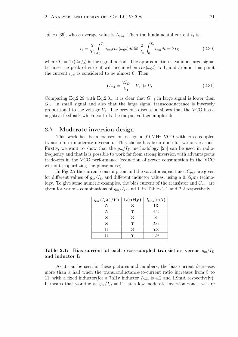
2.7 Moderate inversion designThis work has been focused on design a 910MHz VCO with cross-coupled
transistors in moderate inversion. This choice has been done for various reasons.Firstly, we want to show that the gm/ID methodology [25] can be used in radio-frequency and that is is possible to work far from strong inversion with advantageoustrade-offs in the VCO performance (reduction of power consumption in the VCOwithout jeopardizing the phase noise).
In Fig.2.7 the current consumption and the varactor capacitance Cvar are givenfor different values of gm/ID and different inductor values, using a 0.35µm techno-logy. To give some numeric examples, the bias current of the transistor and Cvar aregiven for various combinations of gm/ID and L in Tables 2.1 and 2.2 respectively.
gm/ID(1/V ) L(nHy) Ibias(mA)5 3 135 7 4.28 3 88 7 2.611 3 5.811 7 1.9
Table 2.1: Bias current of each cross-coupled transistors versus gm/IDand inductor L
As it can be seen in these pictures and numbers, the bias current decreasesmore than a half when the transconductance-to-current ratio increases from 5 to11, with a fixed inductor(for a 7nHy inductor Ibias is 4.2 and 1.9mA respectively).It means that working at gm/ID = 11 -at a low-moderate inversion zone-, we are
22 2.8 Layout design and its consequences in the design methodology
gm/ID(1/V ) L(nHy) Cvar(pF)5 3 5.85 7 2.48 3 3.68 7 1.811 3 1.411 7 1.112 3 0.412 7 0.8
Table 2.2: Capacitance of each varactor versus gm/ID and inductor L
reducing roughly to a half the power consumption. If we were able to work at weakinversion with gm/ID = 17, for example, the bias current would be around 1.3mAfor an L = 7nHy, which is not so lower than the bias current of gm/ID = 11. Thecurrent consumption from moderate inversion to weak inversion does not change somuch but what does increase is the width of the transistor, which rises the transistorcapacitances so much that at gm/ID = 17 the varactor capacitance would be −8pF ,a negative capacitance!.
In case of working in strong inversion the current consumption increases con-siderably. In Sec.3.6 it is shown that the improvement in phase noise when workingin strong inversion does not compensate the increment in the power consumption.
Then it is in moderate inversion where a good trade-off between power con-sumption and physical constrains is observed.
In the Chap.3 it can be seen that the phase noise values in moderate inversionare acceptable to be used in real applications.
2.8 Layout design and its consequences in the design met-hodology
The layout design is a very delicate and difficult task in radio-frequency be-cause lots of effects begin to appear at these bands and commonly they degrade theperformance of the system, specially if a careless layout is done. Some effects are:the appearance of transmission lines, inductive, capacitive and resistive parasitics,the antenna-effect, substrate coupling and others. But which is also true is thatmany of these problems can be considerably reduced if a good layout is performed.
The transmission lines and antenna-effect are almost neglected if the higherdimensions of the circuit are below one tenth of the wave length (in the workingband λ/10 ≈ 30mm, which has never exceeded)[40]. The coupling substrate isimportant when more than one circuit with different signals are used, for examplewhen a power amplifier and a VCO are used, both circuits have to be shielded usinga guard ring connected to ground, to effectively fix the substrate to the groundvoltage [41].
2. Analysis and design of -Gm LC VCOs 23
In case of the parasitics of the interconnecting wires we only considered theirparasitic capacitances and not their resistance parasitics because most of the wiresof the design are short and the ones that are a bit more long were made wide enoughto be discarded the resistive effect. For example, the metal wire that connects thedrains of the transistors nMOS and pMOS has a length of 100µm and a widthof 10µm approximately, and is one of the largest traces of the circuit. The sheetresistance of the metal is 70mΩsquare, then the total resistance of this trace is around0.7Ω. For a bias current of 1mA the voltage drop between the drains is around0.7mV , negligible respect of the signals of the VCO.
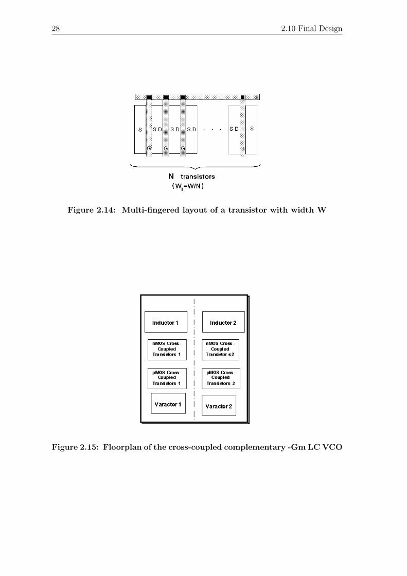
Regarding the transistors, as the width W of them is very large (hundredsof µm), the gate resistance due to the resistive poly-silicon and the contacts hasa considerable value. To decrease this resistance a multi-fingered layout has beenmade, which means that N transistors with a width of W/N are all connected inparallel, as it is seen in Fig.2.14. As the gate resistance of each transistor is inparallel with the other gates, the result resistance is around N times smaller thanthe simple structure. However this kind of layout needs a lot of interconnectionwires which increases the parasitic capacitances.
From what has been discussed, in the design methodology the layout parasiticshave to be considered. In this work, the resistances of the multi-fingered structuretransistors and of the wires are not considered in the methodology. Also the para-sitic inductances are neglected. Therefore the unique parasitics considered are thecapacitances. The following is a detailed discussion on this matter.
Due of the need of maintaining the symmetry of the cross-coupled complemen-tary architecture, the layout has been disposed with an axial symmetry as it is inFig.2.15. This disposition is of great importance specially in terms of phase noiseminimization.
Parasitic capacitancesThe 900MHz -Gm LC VCO designed in this work occupies an important
amount of silicon area because:
1. the inductors are quite big (each one can take tenths of thousands of µm2)because the working frequency is not too high.
2. as the varactor capacitance has been implemented with a MOS transistor, toreach the wanted capacitance the varactor width is considerable.
3. as the transistors were designed to work in moderate inversion they have widthsof hundreds of µm.
The influence of these three blocks in the total parasitic capacitances are con-sidered separately to study their influence. We took care of these parasitics in thepost-layout stage by adjusting the varactor size to achieve the wanted frequency.
The inductors’ parasitic capacitances will be studied in Chap.4 and these arequite well-known so they are added from the beginning in the VCO methodologydesign when the inductor parasitics are calculated. But it has to be mentioned that
24 2.9 Current Source design
the traces that carry the signals to the inductors have a non-negligible length whichcause parasitic capacitances.
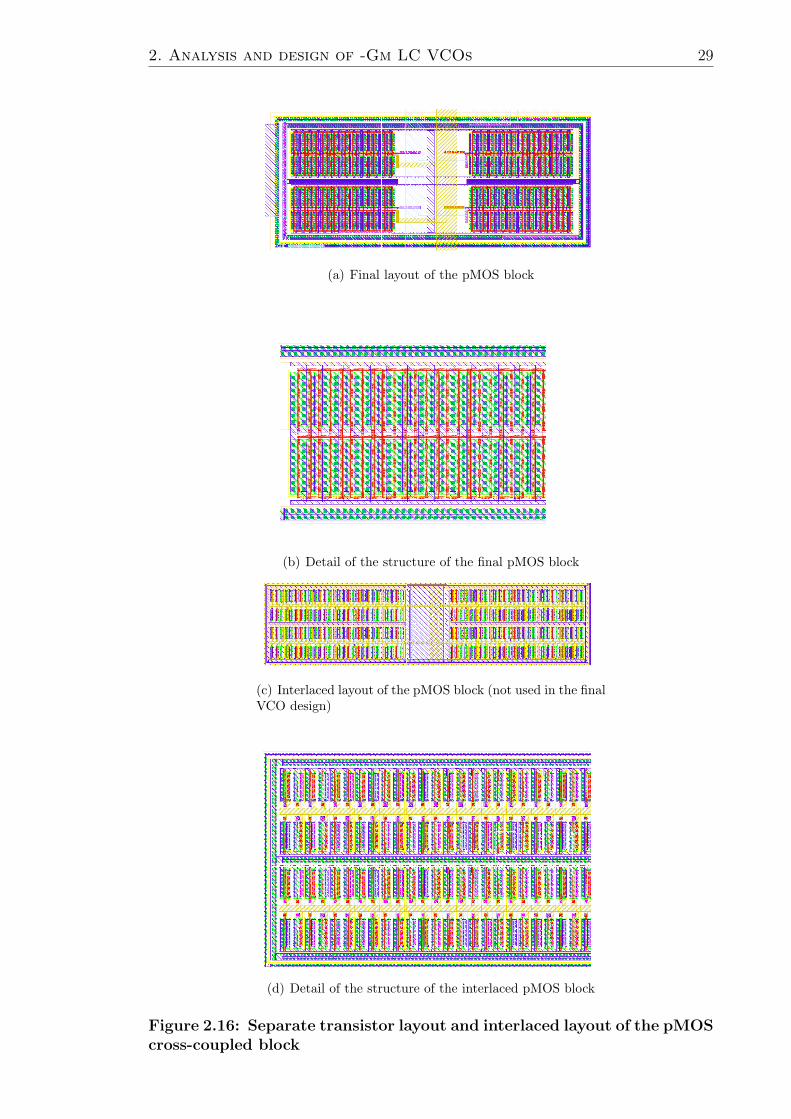
The layout of the cross-coupled transistors can be made in two different ways.One is to design interlaced transistors and the other is to design each transistorseparately. In Figs.2.16(a) and 2.16(c) are depicted the complete view of the separateand interlaced nMOS cross-coupled block, respectively. In the design both have beendone as it is seen in Fig.2.16(a). The former has much more parasitic capacitancesthan the last one because the capacitances that appear with the interconnect wiresincreases considerably the total parasitic capacitances. If the detail of the interlacedlayout of Fig.2.16(b) is compared with the interlaced layout of Fig.2.16(d) it is visiblethat there is a larger quantity of interconnect wires in the former one.
However separate transistors decrease the matching of the gm, despite thelarge size of the transistors diminish this effect. As it is very difficult to estimatethe total parasitic capacitances added by the wires because of the need of severaliterations between the algorithm results and the designed layout, in this work theseparate-transistor architecture has been chosen.
To maintain the symmetry of the layout the varactor has to be divided intotwo parts. The same situation that appeared with the cross-coupled transistorblock is repeated here: each transistor of the varactor can be drawn separately orinterlaced with the other one. In this case it has been found that it is even moredifficult to interlace both transistors than in the case before mentioned. Also inthis situation the parasitic capacitances are very large. Then we decide to use theseparate layout in our design. The complete layout and a detail of the connectionsof the multi-fingered transistors are shown in Figs.2.17(a) and 2.17(b), respectively.
2.9 Current Source designThe election of the current source to be used and its design has been studied
in several works (for example in [17] [21]). It has been payed so much attention tothis subject because a bad choice in the type of the source or in the sizing wouldjeopardize the phase noise of the complete VCO.
In [17] it has been shown that the best current source is a current mirror ofpMOS tansistors. Also the size of these transistors has to be as large as possibleto reduce the thermal and 1/f noise because they are inversely proportional to thewidth of the transistor[33][42]. The size of the current souce is W = 2000µm andL = 1µm. The final layout view of the current source is in Fig.2.18
It can be added a capacitor in parallel with the bias current source to reducethe oscillation of the source of the cross-coupled pMOS transistors and thereforethe phase noise, but its drawback is that it decreases the output impedance of thesource voltage VDD making the VCO more susceptible to voltage supply variations[21].
2. Analysis and design of -Gm LC VCOs 25
2.10 Final DesignConsidering the foregoing analysis and design methodology the VCO design
is given in this section. The final election of the variables involved attempted tofulfill the compromise between power consumption and phase noise by working inmoderate inversion, the requirements of output voltage and the maximum areabudget. The considerations of possible technology variations in passive and activedevices have also been considered.
It has been created an algorithm in Matlab [43] that implements the designmethodology proposed in Fig.2.8. The design has been done in a 0.35µm CMOSstandard technology; the supply voltage used is VDD = 3 Volts and the centralfrequency is 915MHz. The design space has been obtained varying the inductor andthe gm/ID. This election has been done because:
• the inductor is a difficult component whose characteristics -series resistanceand quality factor- modifies substantially the behaviour of the VCO;
• the transconductance-to-current ratio variation modifies the current consump-tion and the transistor size.
Also with the series resistance of the inductor it can be obtained the gm of thetransistors and with the gm/ID the drain current needed. And finally, as it has beensaid previously, we want to test the gm/ID methodology [25] in this kind of circuits.
In the design we use a limited number of these variables: L varies between3nHy and 7nHy at steps of 1nHy, and gm/ID[1/V ] goes from 5 to 17, at stepsof 1V −1. We considered that, due to the variations in the technology, a smallersimulated step would not be neither useful nor clear. The final design values ofgm/ID and L obtained from the algorithm are given in Table 2.3.
Design Parameter ValueL (nHy) 5gm/ID 11
Table 2.3: Final values of L and gm/ID obtained from the implementedalgorithm
As we would like to design the VCO transistors in moderate inversion arisethe problem discussed in Sec.2.8: the value of Cvar. In this particular design thevariable that fundamentally limits is the Cvar, as it can be seen in Table 2.2. TheCvar decreases very rapidly after gm/ID = 11 as it is shown in Fig.2.13(b) so a goodcompromise has been found in this value.
The transistor length is the minimum of the technology: 0.35µm to have themaximum ft available.
In Table2.4 there are the most important VCO variables:Final Layout
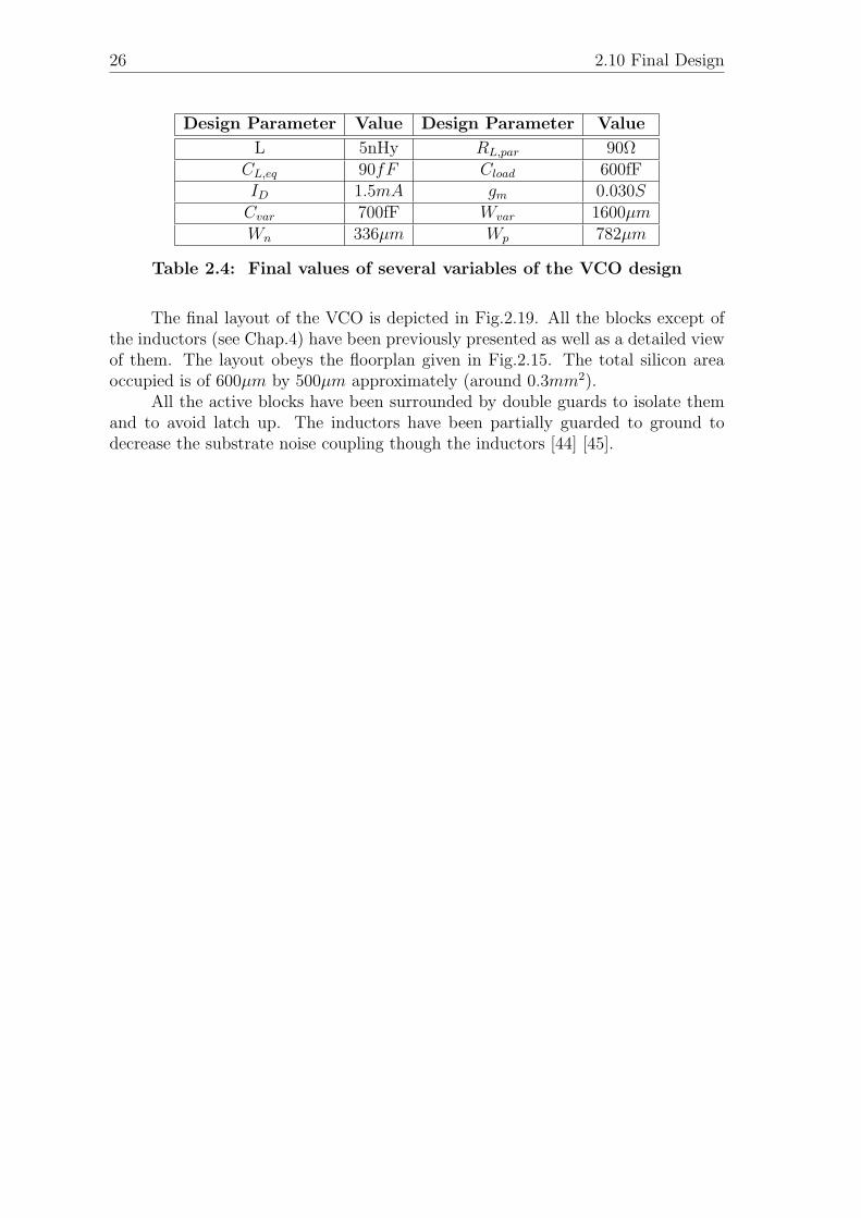
26 2.10 Final Design
Design Parameter Value Design Parameter Value
L 5nHy RL,par 90ΩCL,eq 90fF Cload 600fFID 1.5mA gm 0.030SCvar 700fF Wvar 1600µmWn 336µm Wp 782µm
Table 2.4: Final values of several variables of the VCO design
The final layout of the VCO is depicted in Fig.2.19. All the blocks except ofthe inductors (see Chap.4) have been previously presented as well as a detailed viewof them. The layout obeys the floorplan given in Fig.2.15. The total silicon areaoccupied is of 600µm by 500µm approximately (around 0.3mm2).
All the active blocks have been surrounded by double guards to isolate themand to avoid latch up. The inductors have been partially guarded to ground todecrease the substrate noise coupling though the inductors [44] [45].
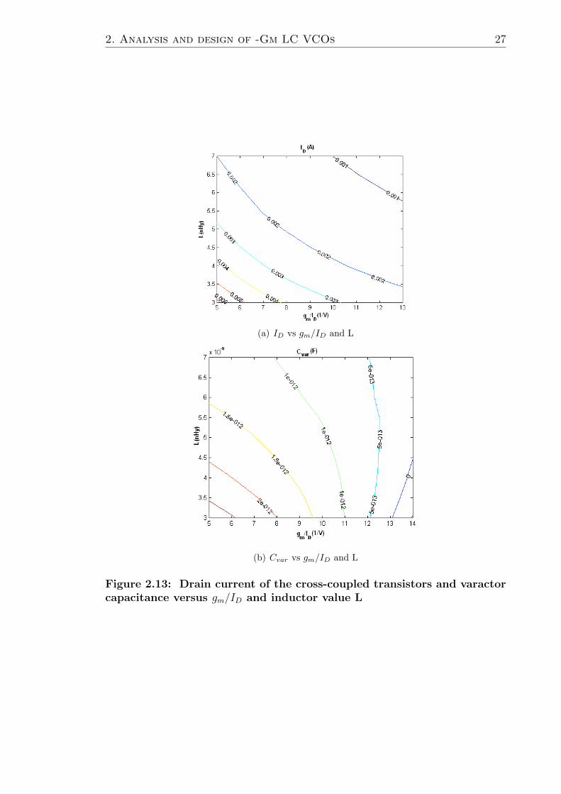
2. Analysis and design of -Gm LC VCOs 27
(a) ID vs gm/ID and L
(b) Cvar vs gm/ID and L
Figure 2.13: Drain current of the cross-coupled transistors and varactorcapacitance versus gm/ID and inductor value L
28 2.10 Final Design
Figure 2.14: Multi-fingered layout of a transistor with width W
Figure 2.15: Floorplan of the cross-coupled complementary -Gm LC VCO
2. Analysis and design of -Gm LC VCOs 29
(a) Final layout of the pMOS block
(b) Detail of the structure of the final pMOS block
(c) Interlaced layout of the pMOS block (not used in the finalVCO design)
(d) Detail of the structure of the interlaced pMOS block
Figure 2.16: Separate transistor layout and interlaced layout of the pMOScross-coupled block
30 2.10 Final Design
(a) General view of the final varactor (the two separate groupof transistors are clearly appreciated)
(b) Detail of the varactor layout showing the multi-fingeredtransistors interconnected
Figure 2.17: Final varactor layout
Figure 2.18: Current source layout
2. Analysis and design of -Gm LC VCOs 31
Figure 2.19: Final layout of the fabricated VCO

32
Chapter 3Phase Noise in LC VCOs
3.1 IntroductionIn this chapter the Phase Noise in electrical oscillators is studied. A general
definition of phase noise for a typical oscillator and particulary expressions of itfor LC-VCO are provided. Also, there are described their most important models,divided in Lineal Time Invariant (LTI) and Lineal Time Variant (LTV) ones. Thenoise sources in the complementary LC-VCO is studied, and expressions of its phasenoise are derived. Finally the calculus and simulation results of the designed -GmLC VCO are shown.
3.2 Phase Noise DefinitionWhen an ideal oscillator is modelled, its output can be expressed as:
Vout = A cos[ω0t+ φ] (3.1)
where amplitude A and arbitrary phase φ are constant values. Therefore, the spec-trum of this signal are two impulses at frequencies ±f0 = ω0
2π, where f0 is the
frequency of oscillation [46].However, when using a real oscillator, the amplitude and the phase are affected
by noise and are time-variant, so the output is now:
Vout(t) = A(t) cos[ω0t+ φ(t)] (3.2)
were φ(t) is called the excess phase of the output. The spectrum of this signal hassidebands close to the frequency of oscillation f0.
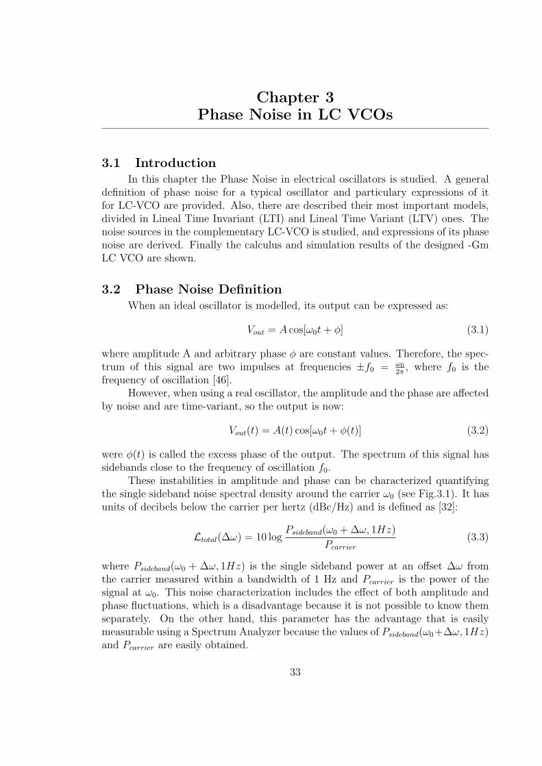
These instabilities in amplitude and phase can be characterized quantifyingthe single sideband noise spectral density around the carrier ω0 (see Fig.3.1). It hasunits of decibels below the carrier per hertz (dBc/Hz) and is defined as [32]:
Ltotal(∆ω) = 10 logPsideband(ω0 + ∆ω, 1Hz)
Pcarrier
(3.3)
where Psideband(ω0 + ∆ω, 1Hz) is the single sideband power at an offset ∆ω fromthe carrier measured within a bandwidth of 1 Hz and Pcarrier is the power of thesignal at ω0. This noise characterization includes the effect of both amplitude andphase fluctuations, which is a disadvantage because it is not possible to know themseparately. On the other hand, this parameter has the advantage that is easilymeasurable using a Spectrum Analyzer because the values of Psideband(ω0+∆ω, 1Hz)and Pcarrier are easily obtained.
33
34 3.3 Review of existing Phase Noise Models
Figure 3.1: Spectrum of the signal around ω0, showing the single sidebandpower at ω0 + ∆ω in grey
In this work it is assumed that the amplitude noise effect is reduced -andalmost eliminated- due to the amplitude-limiting oscillator’s mechanism. But thismechanism does not reduce the phase noise, which is at last, the dominant noisein the oscillator. Then, Ltotal is almost dominated by the effect of the phase noise,and:
Ltotal(∆ω) = Lphase(∆ω) = L(∆ω) (3.4)
Eq.3.3 is the usual definition of the Phase Noise.The phase noise is an important characteristic of the VCO for various reasons.
In a receiver -if it is sufficiently high- less channels can be used in the band as theyinterfere with each other. In transmitters and receivers when a signal is downcon-verted (upconverted) using the output signal of the VCO with high phase noise, thedownconverted (upconverted) signal has lots of components at other unwanted fre-quencies around the frequency of interest. In the transmitters it generates a diffuseconstellation of symbols making difficult to receive them correctly.
3.3 Review of existing Phase Noise ModelsVarious models have been developed to explain and describe the behaviour of
the phase noise in oscillators. Two of the most important are the Leeson’s model[47] and the one developed by Hajimiri and Lee [46]. The difference between them isthat the former is a Linear Time Invariant empirical model (from now on LTI) whilethe last one is Linear Time Variant physically based model (LTV). In this sectionboth models are briefly explained and their fundamental phase noise equations areshown.
3.3.1 Linear time invariant model
The models described in this section study the phase noise of an LC-oscillator.This circuit, visualized in Fig.3.2 is composed by a tank formed by the parallel of an
3. Phase Noise in LC VCOs 35
Figure 3.2: RLC oscillator
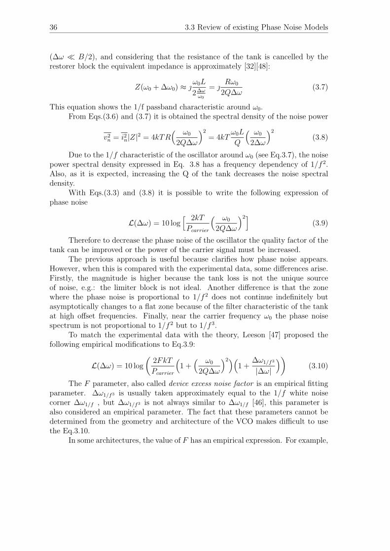
Figure 3.3: Equivalent tank impedance value.
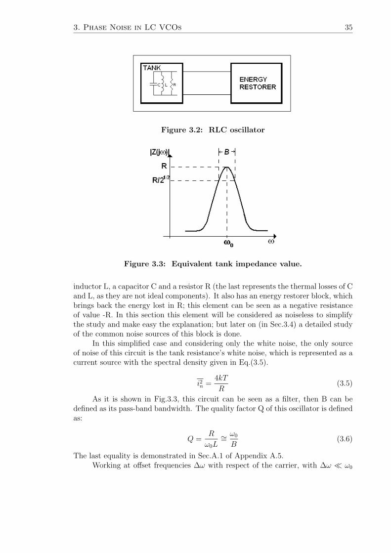
inductor L, a capacitor C and a resistor R (the last represents the thermal losses of Cand L, as they are not ideal components). It also has an energy restorer block, whichbrings back the energy lost in R; this element can be seen as a negative resistanceof value -R. In this section this element will be considered as noiseless to simplifythe study and make easy the explanation; but later on (in Sec.3.4) a detailed studyof the common noise sources of this block is done.
In this simplified case and considering only the white noise, the only sourceof noise of this circuit is the tank resistance’s white noise, which is represented as acurrent source with the spectral density given in Eq.(3.5).
i2n =4kT
R(3.5)
As it is shown in Fig.3.3, this circuit can be seen as a filter, then B can bedefined as its pass-band bandwidth. The quality factor Q of this oscillator is definedas:
Q =R
ω0L∼=ω0
B(3.6)
The last equality is demonstrated in Sec.A.1 of Appendix A.5.Working at offset frequencies ∆ω with respect of the carrier, with ∆ω ω0
36 3.3 Review of existing Phase Noise Models
(∆ω B/2), and considering that the resistance of the tank is cancelled by therestorer block the equivalent impedance is approximately [32][48]:
Z(ω0 + ∆ω0) ≈ ω0L
2∆ωω0
= Rω0
2Q∆ω(3.7)
This equation shows the 1/f passband characteristic around ω0.From Eqs.(3.6) and (3.7) it is obtained the spectral density of the noise power
v2n = i2n|Z|2 = 4kTR
( ω0
2Q∆ω
)2
= 4kTω0L
Q
( ω0
2∆ω
)2
(3.8)
Due to the 1/f characteristic of the oscillator around ω0 (see Eq.3.7), the noisepower spectral density expressed in Eq. 3.8 has a frequency dependency of 1/f2.Also, as it is expected, increasing the Q of the tank decreases the noise spectraldensity.
With Eqs.(3.3) and (3.8) it is possible to write the following expression ofphase noise
L(∆ω) = 10 log[ 2kT
Pcarrier
( ω0
2Q∆ω
)2](3.9)
Therefore to decrease the phase noise of the oscillator the quality factor of thetank can be improved or the power of the carrier signal must be increased.
The previous approach is useful because clarifies how phase noise appears.However, when this is compared with the experimental data, some differences arise.Firstly, the magnitude is higher because the tank loss is not the unique sourceof noise, e.g.: the limiter block is not ideal. Another difference is that the zonewhere the phase noise is proportional to 1/f2 does not continue indefinitely butasymptotically changes to a flat zone because of the filter characteristic of the tankat high offset frequencies. Finally, near the carrier frequency ω0 the phase noisespectrum is not proportional to 1/f2 but to 1/f3.
To match the experimental data with the theory, Leeson [47] proposed thefollowing empirical modifications to Eq.3.9:
L(∆ω) = 10 log
(2FkT
Pcarrier
(1 +
( ω0
2Q∆ω
)2)(1 +
∆ω1/f3
|∆ω|
))(3.10)
The F parameter, also called device excess noise factor is an empirical fittingparameter. ∆ω1/f3 is usually taken approximately equal to the 1/f white noisecorner ∆ω1/f , but ∆ω1/f3 is not always similar to ∆ω1/f [46], this parameter isalso considered an empirical parameter. The fact that these parameters cannot bedetermined from the geometry and architecture of the VCO makes difficult to usethe Eq.3.10.
In some architectures, the value of F has an empirical expression. For example,

3. Phase Noise in LC VCOs 37
Figure 3.4: Asymptotic graphic of Phase Noise.
for a LC differential VCO it is possible to use the following expression [38]
F = 2 +8γTIbias
πV0
+ γ8
9gmbiasR (3.11)
where γ is called noise factor of a MOSFET; for a long channel MOSFET its valueis typical 2/3 and for a short channel one it is approximately 2.5 [49](these valuesdepend also on the inversion level; an interesting study of this matter is given in[35]). Ibias is the current given by the current source; V0 is the VCO output voltage;R is the equivalent resistance of the VCO; and gmbias is the transconductance of thebias transistor.4
The Leeson’s model expressed in Eq.3.10 is a linear time invariant model whichestimates much better the phase noise spectrum compared with Eq.3.9. However ithas the drawback of being an empirical model and without any data from the VCOarchitecture behaviour (∆ω1/f3 or F), this model cannot make any quantitativepredictions.
It is not the case of LC-VCO’s, where approximated expressions of the Fparameter exist and good phase noise estimations are possible.
3.3.2 A linear time varying phase noise theory
This theory has been presented by Ali Hajimiri and Thomas Lee [32][39][46]and attempts to give a quantitative explanation of the phase noise of VCOs. It isnot the idea of this section to explain deeply the complete theory but to give a briefinsight into it and to show the most important results.
In the cited works there are revised two hypothesis used in the Lesson’s model:
4The first term of F equation arise from the tank noise, the second is deduced from the diffe-rential pair noise and the last one is caused by the bias current noise. An interesting deduction ofthese terms is given in [38]
38 3.3 Review of existing Phase Noise Models
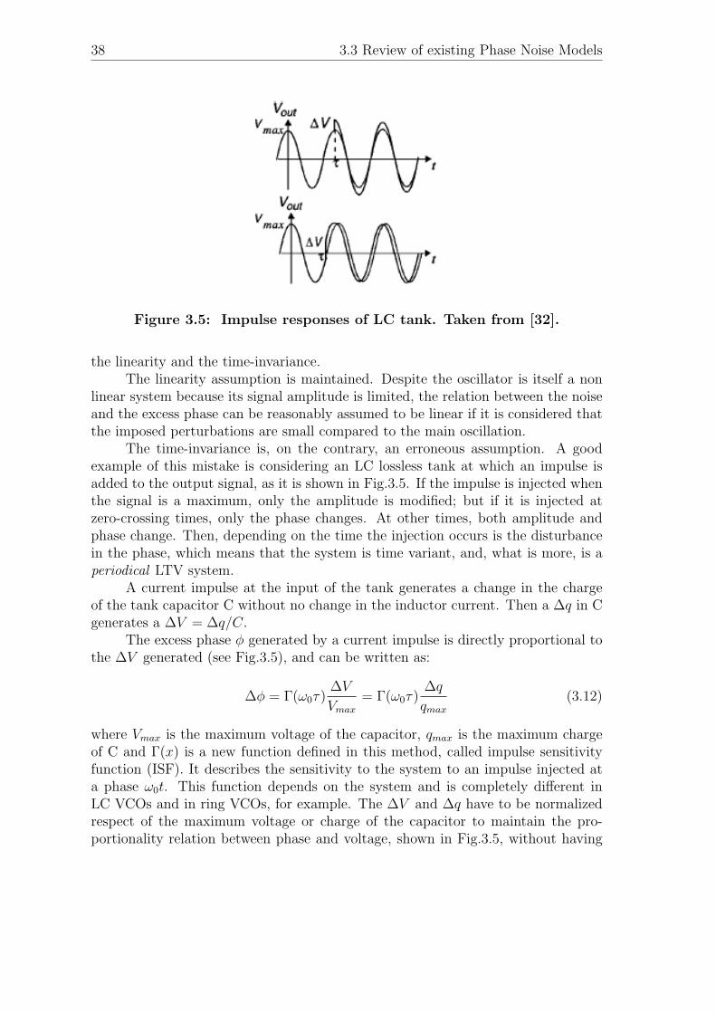
Figure 3.5: Impulse responses of LC tank. Taken from [32].
the linearity and the time-invariance.The linearity assumption is maintained. Despite the oscillator is itself a non
linear system because its signal amplitude is limited, the relation between the noiseand the excess phase can be reasonably assumed to be linear if it is considered thatthe imposed perturbations are small compared to the main oscillation.
The time-invariance is, on the contrary, an erroneous assumption. A goodexample of this mistake is considering an LC lossless tank at which an impulse isadded to the output signal, as it is shown in Fig.3.5. If the impulse is injected whenthe signal is a maximum, only the amplitude is modified; but if it is injected atzero-crossing times, only the phase changes. At other times, both amplitude andphase change. Then, depending on the time the injection occurs is the disturbancein the phase, which means that the system is time variant, and, what is more, is aperiodical LTV system.
A current impulse at the input of the tank generates a change in the chargeof the tank capacitor C without no change in the inductor current. Then a ∆q in Cgenerates a ∆V = ∆q/C.
The excess phase φ generated by a current impulse is directly proportional tothe ∆V generated (see Fig.3.5), and can be written as:
∆φ = Γ(ω0τ)∆V
Vmax
= Γ(ω0τ)∆q
qmax
(3.12)
where Vmax is the maximum voltage of the capacitor, qmax is the maximum chargeof C and Γ(x) is a new function defined in this method, called impulse sensitivityfunction (ISF). It describes the sensitivity to the system to an impulse injected ata phase ω0t. This function depends on the system and is completely different inLC VCOs and in ring VCOs, for example. The ∆V and ∆q have to be normalizedrespect of the maximum voltage or charge of the capacitor to maintain the pro-portionality relation between phase and voltage, shown in Fig.3.5, without having
3. Phase Noise in LC VCOs 39
units.To understand the behaviour of these kind of systems the unit impulse res-
ponse for the excess phase is studied . This function will be used to show how themechanism of the phase noise works.
Maintaining the same form as the excess phase of Eq.3.12, the impulse responsecan be written as follows:
hφ(t, τ) =Γ(ω0τ)
qmax
u(t− τ) (3.13)
where u(t) is the unit step function.For a input current i(t) the excess phase can be calculated as follows:
φ(t) =
∫ ∞
−∞hφ(t, τ)i(τ)dτ =
1
qmax
∫ t
−∞Γ(ω0τ)i(τ)dτ (3.14)
As Γ(x) is a periodical function it can be expressed by Fourier series withcoefficients cn. If its cn coefficients are known, the excess phase is:
φ(t) =1
qmax
[c02
∫ t
−∞i(τ)dτ +
∞∑n=1
cn
∫ t
−∞i(τ) cos(nω0τ)dτ
](3.15)
It is known that noise at a certain frequency, injected into an oscillator, produ-ces spectral components at other frequencies. To demonstrate this property, i(t) isconsidered to be a sinusoidal current source with phase (mω0 + ∆ω)t , where mω0,with m = 1..∞ is a frequency multiple of the oscillator frequency and, as it hasbeen used in this chapter, ∆ω << ω0. All the integrals of the terms in Eq.3.15 arenegligible except when n=m. Then the excess phase noise results in the followingapproximate expression:
φ(t) ≈ Imcm sin(∆ωt)
2qmax∆ω(3.16)
with the coefficients cm used previously (with n=m).It shows that the spectrum of φ(t) are two impulses at ±∆ω, despite the
spectrum of the imposed signal is at frequency mω0.With Eq. 3.15 the spectrum of φ(t) can be obtained, but what is really im-
portant is the spectrum of the output signal as a function of φ(t). This change iscalled phase to voltage conversion, and it is a modulation of the excess phase thatappears in the output signal.
A clarifying scheme of the process is shown in Fig.3.6, considering that theoutput voltage of the system is sinusoidal. If no perturbation appears the outputvoltage is vout = sin(ω0t) and no phase modulation appears. But if a current pertur-bation i(t) exists, then an excess phase φ(t) appears in the system (the normalizedi(t)is multiplied by the ISF function at ω0t, obtaining ψ(t) and then integrated toobtain φ(t)). This excess phase is added to ω0t, the initial phase of the system.
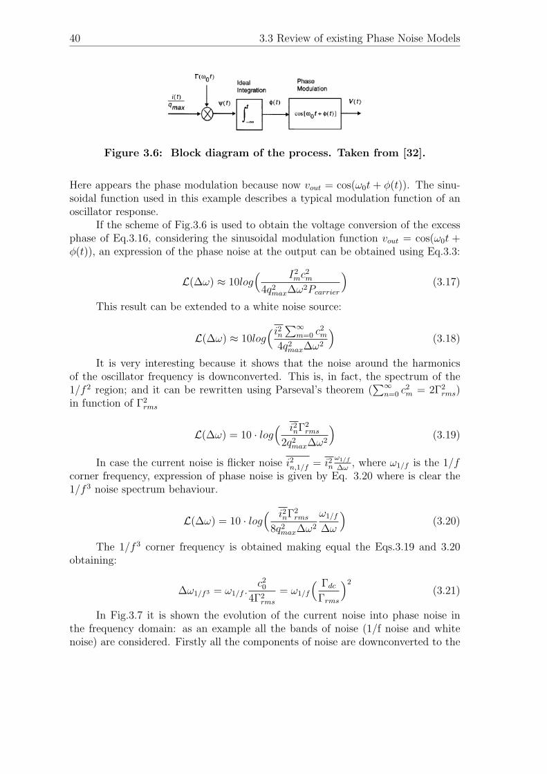
40 3.3 Review of existing Phase Noise Models
Figure 3.6: Block diagram of the process. Taken from [32].
Here appears the phase modulation because now vout = cos(ω0t + φ(t)). The sinu-soidal function used in this example describes a typical modulation function of anoscillator response.
If the scheme of Fig.3.6 is used to obtain the voltage conversion of the excessphase of Eq.3.16, considering the sinusoidal modulation function vout = cos(ω0t +φ(t)), an expression of the phase noise at the output can be obtained using Eq.3.3:
L(∆ω) ≈ 10log( I2
mc2m
4q2max∆ω
2Pcarrier
)(3.17)
This result can be extended to a white noise source:
L(∆ω) ≈ 10log( i2n ∑∞
m=0 c2m
4q2max∆ω
2
)(3.18)
It is very interesting because it shows that the noise around the harmonicsof the oscillator frequency is downconverted. This is, in fact, the spectrum of the1/f2 region; and it can be rewritten using Parseval’s theorem (
∑∞n=0 c
2m = 2Γ2
rms)in function of Γ2
rms
L(∆ω) = 10 · log( i2nΓ2
rms
2q2max∆ω
2
)(3.19)
In case the current noise is flicker noise i2n,1/f = i2nω1/f
∆ω, where ω1/f is the 1/f
corner frequency, expression of phase noise is given by Eq. 3.20 where is clear the1/f3 noise spectrum behaviour.
L(∆ω) = 10 · log( i2nΓ2
rms
8q2max∆ω
2
ω1/f
∆ω
)(3.20)
The 1/f3 corner frequency is obtained making equal the Eqs.3.19 and 3.20obtaining:
∆ω1/f3 = ω1/f .c20
4Γ2rms
= ω1/f
( Γdc
Γrms
)2
(3.21)
In Fig.3.7 it is shown the evolution of the current noise into phase noise inthe frequency domain: as an example all the bands of noise (1/f noise and whitenoise) are considered. Firstly all the components of noise are downconverted to the
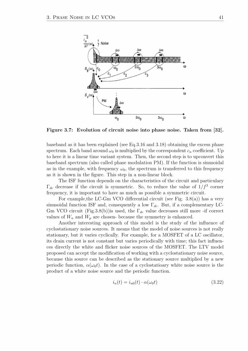
3. Phase Noise in LC VCOs 41
Figure 3.7: Evolution of circuit noise into phase noise. Taken from [32].
baseband as it has been explained (see Eq.3.16 and 3.18) obtaining the excess phasespectrum. Each band around ω0 is multiplied by the correspondent cn coefficient. Upto here it is a linear time variant system. Then, the second step is to upconvert thisbaseband spectrum (also called phase modulation PM). If the function is sinusoidalas in the example, with frequency ω0, the spectrum is transferred to this frequencyas it is shown in the figure. This step in a non-linear block.
The ISF function depends on the characteristics of the circuit and particularyΓdc decrease if the circuit is symmetric. So, to reduce the value of 1/f3 cornerfrequency, it is important to have as much as possible a symmetric circuit.
For example,the LC-Gm VCO differential circuit (see Fig. 3.8(a)) has a verysinusoidal function ISF and, consequently a low Γdc. But, if a complementary LC-Gm VCO circuit (Fig.3.8(b))is used, the Γdc value decreases still more -if correctvalues of Wn and Wp are chosen- because the symmetry is enhanced.
Another interesting approach of this model is the study of the influence ofcyclostationary noise sources. It means that the model of noise sources is not reallystationary, but it varies cyclically. For example, for a MOSFET of a LC oscillator,its drain current is not constant but varies periodically with time; this fact influen-ces directly the white and flicker noise sources of the MOSFET. The LTV modelproposed can accept the modification of working with a cyclostationary noise source,because this source can be described as the stationary source multiplied by a newperiodic function, α(ω0t). In the case of a cyclostatioary white noise source is theproduct of a white noise source and the periodic function.
in(t) = in0(t) · α(ω0t) (3.22)
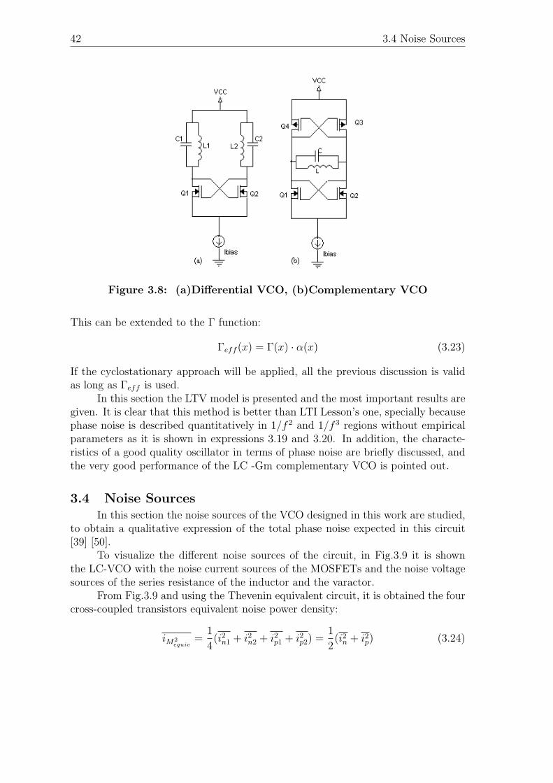
42 3.4 Noise Sources
Figure 3.8: (a)Differential VCO, (b)Complementary VCO
This can be extended to the Γ function:
Γeff (x) = Γ(x) · α(x) (3.23)
If the cyclostationary approach will be applied, all the previous discussion is validas long as Γeff is used.
In this section the LTV model is presented and the most important results aregiven. It is clear that this method is better than LTI Lesson’s one, specially becausephase noise is described quantitatively in 1/f2 and 1/f3 regions without empiricalparameters as it is shown in expressions 3.19 and 3.20. In addition, the characte-ristics of a good quality oscillator in terms of phase noise are briefly discussed, andthe very good performance of the LC -Gm complementary VCO is pointed out.
3.4 Noise SourcesIn this section the noise sources of the VCO designed in this work are studied,
to obtain a qualitative expression of the total phase noise expected in this circuit[39] [50].
To visualize the different noise sources of the circuit, in Fig.3.9 it is shownthe LC-VCO with the noise current sources of the MOSFETs and the noise voltagesources of the series resistance of the inductor and the varactor.
From Fig.3.9 and using the Thevenin equivalent circuit, it is obtained the fourcross-coupled transistors equivalent noise power density:
iM2equiv
=1
4(i2n1 + i2n2 + i2p1 + i2p2) =
1
2(i2n + i2p) (3.24)
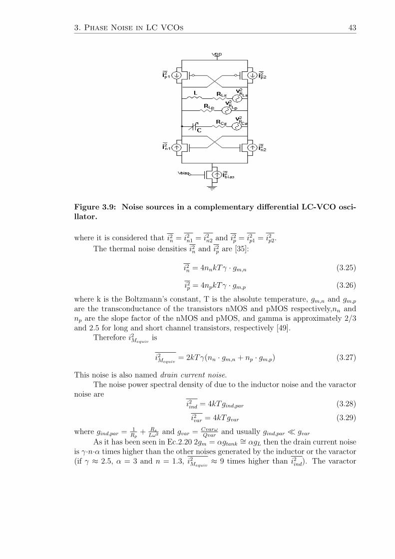
3. Phase Noise in LC VCOs 43
Figure 3.9: Noise sources in a complementary differential LC-VCO osci-llator.
where it is considered that i2n = i2n1 = i2n2 and i2p = i2p1 = i2p2.
The thermal noise densities i2n and i2p are [35]:
i2n = 4nnkTγ · gm,n (3.25)
i2p = 4npkTγ · gm,p (3.26)
where k is the Boltzmann’s constant, T is the absolute temperature, gm,n and gm,p
are the transconductance of the transistors nMOS and pMOS respectively,nn andnp are the slope factor of the nMOS and pMOS, and gamma is approximately 2/3and 2.5 for long and short channel transistors, respectively [49].
Therefore i2Mequivis
i2Mequiv= 2kTγ(nn · gm,n + np · gm,p) (3.27)
This noise is also named drain current noise.The noise power spectral density of due to the inductor noise and the varactor
noise arei2ind = 4kTgind,par (3.28)
i2var = 4kTgvar (3.29)
where gind,par = 1Rp
+ Rs
Lω2 and gvar = CvarωQvar
and usually gind,par gvar
As it has been seen in Ec.2.20 2gm = αgtank∼= αgL then the drain current noise
is γ·n·α times higher than the other noises generated by the inductor or the varactor(if γ ≈ 2.5, α = 3 and n = 1.3, i2Mequiv
≈ 9 times higher than i2ind). The varactor
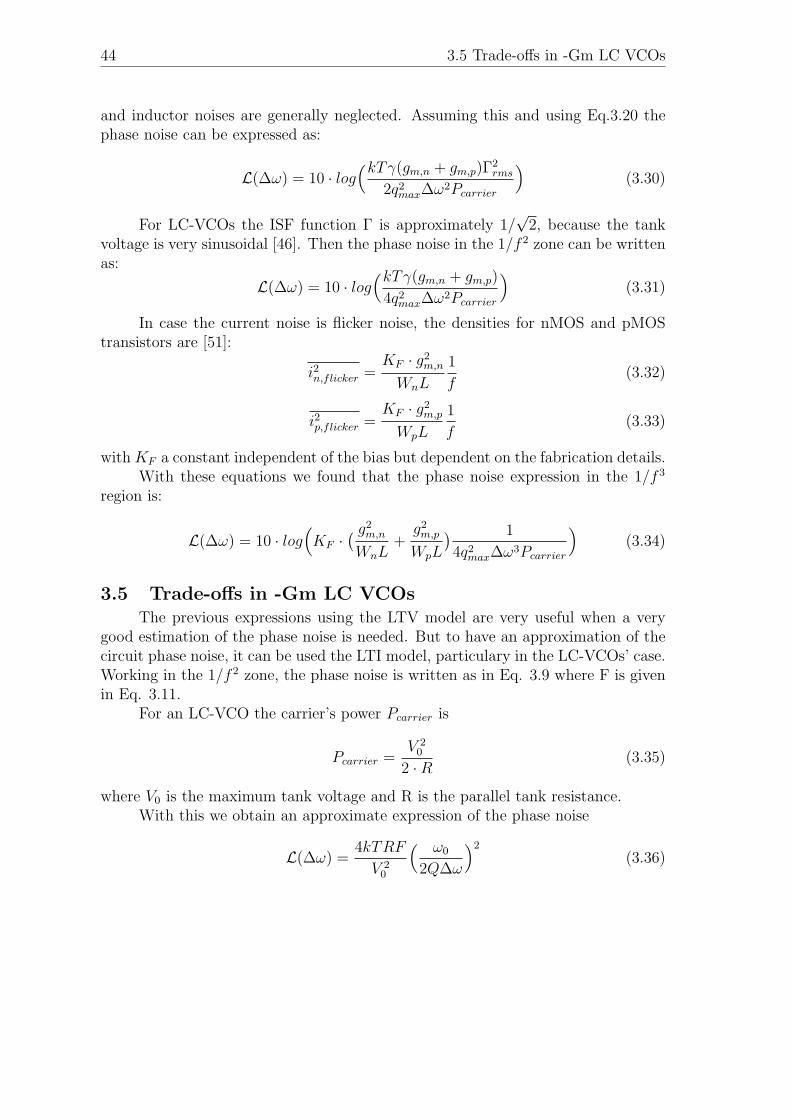
44 3.5 Trade-offs in -Gm LC VCOs
and inductor noises are generally neglected. Assuming this and using Eq.3.20 thephase noise can be expressed as:
L(∆ω) = 10 · log(kTγ(gm,n + gm,p)Γ
2rms
2q2max∆ω
2Pcarrier
)(3.30)
For LC-VCOs the ISF function Γ is approximately 1/√
2, because the tankvoltage is very sinusoidal [46]. Then the phase noise in the 1/f2 zone can be writtenas:
L(∆ω) = 10 · log(kTγ(gm,n + gm,p)
4q2max∆ω
2Pcarrier
)(3.31)
In case the current noise is flicker noise, the densities for nMOS and pMOStransistors are [51]:
i2n,flicker =KF · g2
m,n
WnL
1
f(3.32)
i2p,flicker =KF · g2
m,p
WpL
1
f(3.33)
withKF a constant independent of the bias but dependent on the fabrication details.With these equations we found that the phase noise expression in the 1/f3
region is:
L(∆ω) = 10 · log(KF ·
( g2m,n
WnL+g2
m,p
WpL
) 1
4q2max∆ω
3Pcarrier
)(3.34)
3.5 Trade-offs in -Gm LC VCOsThe previous expressions using the LTV model are very useful when a very
good estimation of the phase noise is needed. But to have an approximation of thecircuit phase noise, it can be used the LTI model, particulary in the LC-VCOs’ case.Working in the 1/f2 zone, the phase noise is written as in Eq. 3.9 where F is givenin Eq. 3.11.
For an LC-VCO the carrier’s power Pcarrier is
Pcarrier =V 2
0
2 ·R(3.35)
where V0 is the maximum tank voltage and R is the parallel tank resistance.With this we obtain an approximate expression of the phase noise
L(∆ω) =4kTRF
V 20
( ω0
2Q∆ω
)2
(3.36)

3. Phase Noise in LC VCOs 45
which can be re-written using the gm/Id factor as
L(∆ω) =kTπ2
32
F
α
1
Q2
gm/IdIbias
( ω0
∆ω
)2
(3.37)
In Appendix A.5, Sec.A.2 is explained how to obtain the last equation.It has been studied -using the Eq.3.37- the dependence of the VCO’s phase
noise with the intrinsic parameters of the inductor: Q, L and RL,par.
• For a VCO with L = 5nH, C = 6pF , Ibias = 2mA,VDD = 3V and f0 =910MHz and a ∆ω = 600kHz 5, its phase noise is plotted using Eq.3.37(seeFig. 3.10) when varying RL,par. As it is shown in the Eq.A.20 of AppendixA.5 the parallel resistance RL,par of the inductor is proportional to the qualityfactor Q. If increases RL,par, increases Q, which results in a reduction of thephase noise.
• In Fig. 3.11 it is shown the behaviour of the phase noise when varying theinductance value, for a VCO with fixed Q = 3; VDD = 3V , f0 = 910MHz,Ibias = 2mA and C = 6pF . As Q = RL,par/wL (refer to Eq.A.20), if Q isfixed 6and L is raised then RL,par must increase. This leads to the previousdiscussion about the consequences of rise RL,par An increment in L in thementioned conditions leads to a lower phase noise.
• Now it is considered a similar situation with identical parameters’ values, butnow a fixed inductor L is used and the Q of the inductor varies. The phasenoise decreases as Q is raised. A plot of the phase noise as a function of Q isshown in Fig.3.12.
A general conclusion from these results is that having an inductor with a highQ improves the phase noise. If the inductor is off-chip it can be achieved easily, butit is not the case of the monolithic inductors. Also, it is true that increasing theinductor value decreases the phase noise, but this only happens when the Q is fixed;this is difficult to be done because generally increasing the size of the inductor leadsto high losses, and then lower Q. These facts will be seen in Chapter 4.
The previous approach only considers the minimization of the phase noise ina VCO design. A more realistic approach is to consider not only the phase noiseminimization but also the imposed specifications of the power consumption. Then,it is possible to define a figure of merit FOM which takes into account the powerconsumption Pd and the phase noise in an offset band ∆ω from ω0 [52]. This figureof merit has to be minimized in order to obtain high performance (low phase noiseand low power consumption). It is defined as:
FOM = L(∆ω)Pd
(∆ω
ω0
)2
(3.38)
5The phase noise at this ∆ω value is usually specified in the published works and in theIEEE802.15.4 power specifications are given at this frequency
6It is not a typical case
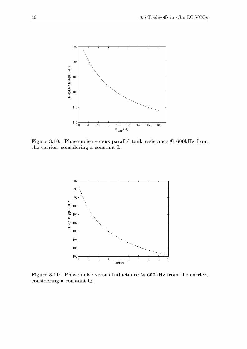
46 3.5 Trade-offs in -Gm LC VCOs
Figure 3.10: Phase noise versus parallel tank resistance @ 600kHz fromthe carrier, considering a constant L.
Figure 3.11: Phase noise versus Inductance @ 600kHz from the carrier,considering a constant Q.
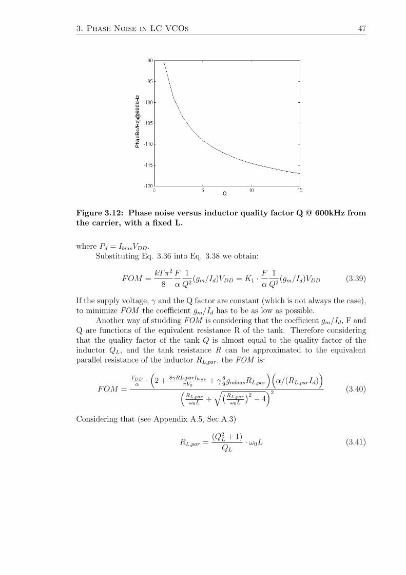
3. Phase Noise in LC VCOs 47
Figure 3.12: Phase noise versus inductor quality factor Q @ 600kHz fromthe carrier, with a fixed L.
where Pd = IbiasVDD.Substituting Eq. 3.36 into Eq. 3.38 we obtain:
FOM =kTπ2
8
F
α
1
Q2(gm/Id)VDD = K1 ·
F
α
1
Q2(gm/Id)VDD (3.39)
If the supply voltage, γ and the Q factor are constant (which is not always the case),to minimize FOM the coefficient gm/Id has to be as low as possible.
Another way of studding FOM is considering that the coefficient gm/Id, F andQ are functions of the equivalent resistance R of the tank. Therefore consideringthat the quality factor of the tank Q is almost equal to the quality factor of theinductor QL, and the tank resistance R can be approximated to the equivalentparallel resistance of the inductor RL,par, the FOM is:
FOM =
VDD
α·(2 + 8γRL,parIbias
πV0+ γ 8
9gmbiasRL,par
)(α/(RL,parId)
)(
RL,par
ω0L+
√(RL,par
ω0L
)2 − 4)2 (3.40)
Considering that (see Appendix A.5, Sec.A.3)
RL,par =(Q2
L + 1)
QL
· ω0L (3.41)
48 3.6 Phase Noise results obtained from simulation
the Eq.3.39 can be re-written as
FM =2VDD
(2 +
(8γIbias
πV0+ γ 8
9gmbias
)· (Q2
L+1)
QL· ω0L
)ω0LQL(Q2
L + 1)(3.42)
Considering only variations of the tank parameters, in Fig. 3.5 it is shownthe FOM as a function of Rs (series resistance of the inductor), Q and RL,par foran arbitrary set of parameters: VDD = 3V , L=5nHy, f0 = 910MHz, Id = 9mA,gmbias = 50mS, α = 3 and with Q varying between 1 and 7. According to thefigures, to obtain a minimum FOM the quality factor of the tank or equivalentlythe inductance’s parallel resistance have to be as high as possible, what is consistentwith decreasing as much as possible the inductance series resistance of the tank.
If only the variation of the gm/ID is considered (with Q = 3, L = 5nHy andf0 = 910MHz) the FOM has the behaviour shown in Fig.3.14. In this figure it isclear that minimizing the FM being equivalent to work in strong inversion.
However, in this work it is shown that a good compromise between phase noiseand power consumption is achieved when working in moderate inversion.
3.6 Phase Noise results obtained from simulationIn this section the results of phase noise calculated in Matlab and simulated
in RF Spectre of Cadence are shown.A Matlab routine has been implemented to calculate the phase noise for a set
of differential cross-coupled VCOs in 0.35µm technology with the following charac-teristics:
• f0 = 910MHz
• gm/ID = (5..17)[S · A]−1
• L = (3..7)nHy
• α = 3
• Cload = 0.6pF
In Fig.3.15 it is plotted the phase noise versus the inductance of the designedVCOs @600kHz from the carrier with the LTI model. It shows that increasing thegm/ID of the cross-coupled transistors or increasing the inductor value (consideringthat the Q varies accordingly) the phase noise of these VCOs is deteriorated. Whenthe gm/ID rise from 5(V )−1 to 17(V )−1 the phase noise increases almost 10dBc/Hz.The reduction of this parameter due to L is not so important, being approximately0.7dBc/Hz.
The VCO finally designed has a theoretic value of gm/ID = 11 and L =5nHy. For this values the phase noise between 16kHz and 3.2MHz is calculatedusing two methods: (1) the LTI method with the Eqs. 3.11 and 3.37 and (2) the
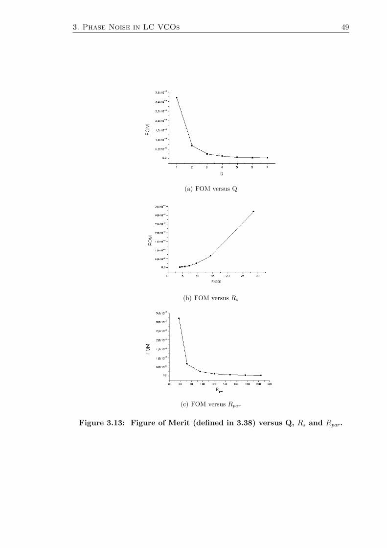
3. Phase Noise in LC VCOs 49
(a) FOM versus Q
(b) FOM versus Rs
(c) FOM versus Rpar
Figure 3.13: Figure of Merit (defined in 3.38) versus Q, Rs and Rpar.

50 3.7 Conclusions
Figure 3.14: Figure of Merit versus gm/ID.
LTV method with Eq.3.31 and that qmax = VmaxCtotal (with Vmax the maximumvoltage of each output node of the tank and Ctotal the total capacitance of thetank). Both results are plotted in 3.6 (the initial value has been chosen long enoughfrom the 1/f3 zone). Both curves are very similar but there is a difference in thephase noise value. At 600kHz from the carrier the phase noise value with the LTImodel is approximately -108dBc/Hz and with the LTV model is -119.7dBc/Hz.The difference can be explained with the noise factor F of the LTI model as itis an empirical value and in this work it has been obtained by an approximatedexpression.
With the Spectre RF tool of Cadence, the phase noise of this circuit has beensimulated and the results are shown in Fig.3.17. The phase noise value at 600kHzfrom the carrier is -121dBc/Hz. There is a great agreement between the phase noisecalculated with the LTV model as it was expected.
3.7 ConclusionsIn this chapter it has been studied the two phase noise theories most utilized
to model this parameter: the linear time invariant and the linear time variant. Ithas been shown that the last one is the most accurate theory to find the phase noiseof an oscillator and that it is possible to calculate it easily for a LC VCO. It hasbeen shown that good agreement between the simulations and the matlab analysis.It also has been shown that low values of phase noise can be achieved with the LCVCO working in moderate inversion.
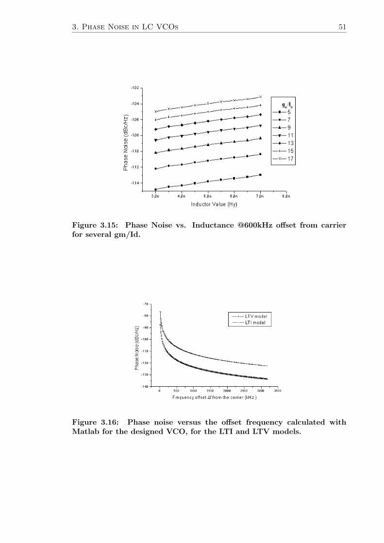
3. Phase Noise in LC VCOs 51
Figure 3.15: Phase Noise vs. Inductance @600kHz offset from carrierfor several gm/Id.
Figure 3.16: Phase noise versus the offset frequency calculated withMatlab for the designed VCO, for the LTI and LTV models.
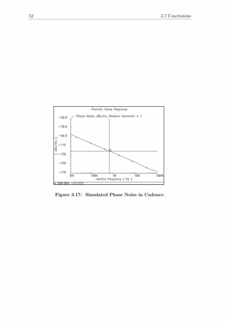
52 3.7 Conclusions
Figure 3.17: Simulated Phase Noise in Cadence.
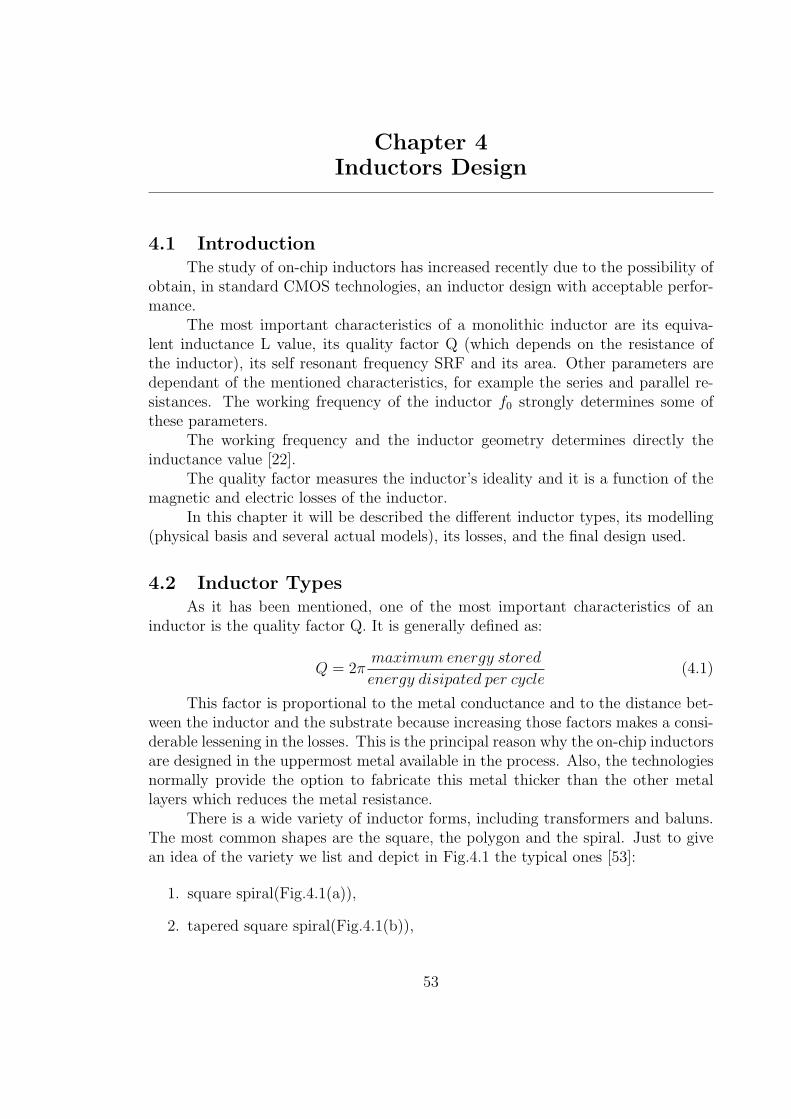
Chapter 4Inductors Design
4.1 IntroductionThe study of on-chip inductors has increased recently due to the possibility of
obtain, in standard CMOS technologies, an inductor design with acceptable perfor-mance.
The most important characteristics of a monolithic inductor are its equiva-lent inductance L value, its quality factor Q (which depends on the resistance ofthe inductor), its self resonant frequency SRF and its area. Other parameters aredependant of the mentioned characteristics, for example the series and parallel re-sistances. The working frequency of the inductor f0 strongly determines some ofthese parameters.
The working frequency and the inductor geometry determines directly theinductance value [22].
The quality factor measures the inductor’s ideality and it is a function of themagnetic and electric losses of the inductor.
In this chapter it will be described the different inductor types, its modelling(physical basis and several actual models), its losses, and the final design used.
4.2 Inductor TypesAs it has been mentioned, one of the most important characteristics of an
inductor is the quality factor Q. It is generally defined as:
Q = 2πmaximum energy stored
energy disipated per cycle(4.1)
This factor is proportional to the metal conductance and to the distance bet-ween the inductor and the substrate because increasing those factors makes a consi-derable lessening in the losses. This is the principal reason why the on-chip inductorsare designed in the uppermost metal available in the process. Also, the technologiesnormally provide the option to fabricate this metal thicker than the other metallayers which reduces the metal resistance.
There is a wide variety of inductor forms, including transformers and baluns.The most common shapes are the square, the polygon and the spiral. Just to givean idea of the variety we list and depict in Fig.4.1 the typical ones [53]:
1. square spiral(Fig.4.1(a)),
2. tapered square spiral(Fig.4.1(b)),
53
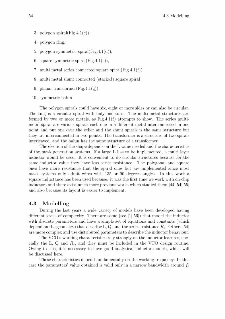
54 4.3 Modelling
3. polygon spiral(Fig.4.1(c)),
4. polygon ring,
5. polygon symmetric spiral(Fig.4.1(d)),
6. square symmetric spiral(Fig.4.1(e)),
7. multi metal series connected square spiral(Fig.4.1(f)),
8. multi metal shunt connected (stacked) square spiral
9. planar transformer(Fig.4.1(g)),
10. symmetric balun.
The polygon spirals could have six, eight or more sides or can also be circular.The ring is a circular spiral with only one turn. The multi-metal structures areformed by two or more metals, as Fig.4.1(f) attempts to show. The series multi-metal spiral are various spirals each one in a different metal interconnected in onepoint and put one over the other and the shunt spirals is the same structure butthey are interconnected in two points. The transformer is a structure of two spiralsinterleaved, and the balun has the same structure of a transformer.
The election of the shape depends on the L value needed and the characteristicsof the mask generation systems. If a large L has to be implemented, a multi layerinductor would be used. It is convenient to do circular structures because for thesame inductor value they have less series resistance. The polygonal and squareones have more resistance that the spiral ones but are implemented since mostmask systems only admit wires with 135 or 90 degrees angles. In this work asquare inductance has been used because: it was the first time we work with on-chipinductors and there exist much more previous works which studied them [44][54][55]and also because its layout is easier to implement.
4.3 ModellingDuring the last years a wide variety of models have been developed having
different levels of complexity. There are some (see [1][56]) that model the inductorwith discrete parameters and have a simple set of equations and constants (whichdepend on the geometry) that describe L, Q, and the series resistance Rs. Others [54]are more complex and use distributed parameters to describe the inductor behaviour.
The VCO’s working characteristics rely strongly on the inductor features, spe-cially the L, Q and Rs, and they must be included in the VCO design routine.Owing to this, it is necessary to have good analytical inductor models, which willbe discussed here.
These characteristics depend fundamentally on the working frequency. In thiscase the parameters’ value obtained is valid only in a narrow bandwidth around f0
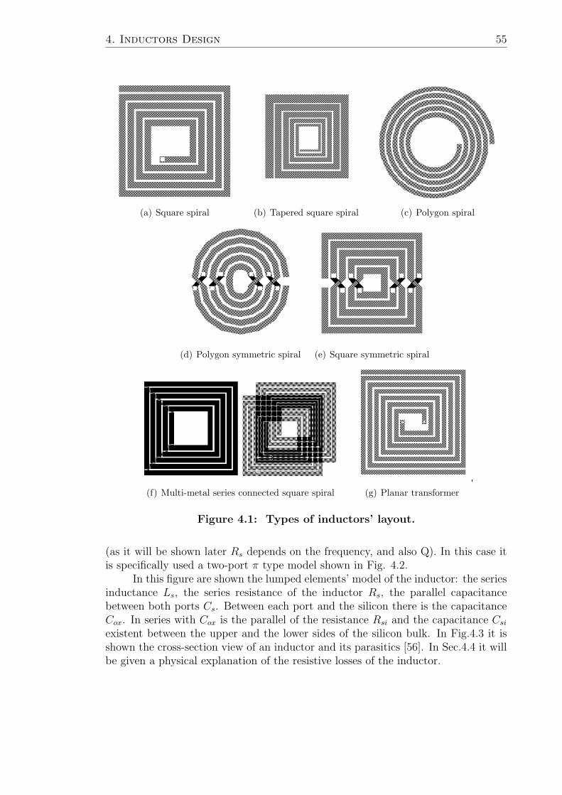
4. Inductors Design 55
(a) Square spiral (b) Tapered square spiral (c) Polygon spiral
(d) Polygon symmetric spiral (e) Square symmetric spiral
(f) Multi-metal series connected square spiral (g) Planar transformer
Figure 4.1: Types of inductors’ layout.
(as it will be shown later Rs depends on the frequency, and also Q). In this case itis specifically used a two-port π type model shown in Fig. 4.2.
In this figure are shown the lumped elements’ model of the inductor: the seriesinductance Ls, the series resistance of the inductor Rs, the parallel capacitancebetween both ports Cs. Between each port and the silicon there is the capacitanceCox. In series with Cox is the parallel of the resistance Rsi and the capacitance Csi
existent between the upper and the lower sides of the silicon bulk. In Fig.4.3 it isshown the cross-section view of an inductor and its parasitics [56]. In Sec.4.4 it willbe given a physical explanation of the resistive losses of the inductor.
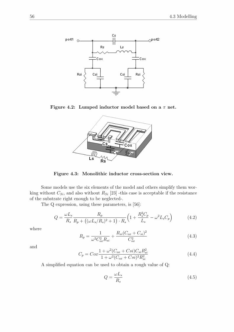
56 4.3 Modelling
Figure 4.2: Lumped inductor model based on a π net.
Figure 4.3: Monolithic inductor cross-section view.
Some models use the six elements of the model and others simplify them wor-king without CSi, and also without RSi [23] -this case is acceptable if the resistanceof the substrate right enough to be neglected-.
The Q expression, using these parameters, is [56]:
Q =ωLs
Rs
Rp
Rp +((ωLs/Rs)2 + 1
)·Rs
(1 +
R2sCp
Ls
− ω2LsCp
)(4.2)
where
Rp =1
ω2C2oxRsi
+Rsi(Cox + Csi)
2
C2ox
(4.3)
and
Cp = Cox1 + ω2(Cox + Csi)CsiR
2si
1 + ω2(Cox + Csi)2R2si
(4.4)
A simplified equation can be used to obtain a rough value of Q:
Q =ωLs
Rs
(4.5)

4. Inductors Design 57
Figure 4.4: Inductor physical parameters: s is the space between wires, wis their width, dout and din are the output and input diameter respectively.
In Fig.4.4 it is shown the principal physical parameters involved in the expres-sions of the lumped elements: the wire width w, the spaces between wires s and theoutput and input diameters dout and din.
The expressions that calculate the lumped elements vary considerably fromone model to the other. Here are resumed two of the most important ones.
Yue’s model [57][58]This work gives expressions of L, Rs, Cs, Cox, Rsi, Csi in function of the induc-
tor’s geometry. In case of the L value, it is obtained using the Greenhouse algorithm[59]. The other elements’ expressions, working with a four-metal technology, are:
Rs =ρ.l
w.δ.(1− e−tδ )
(4.6)
Cs = n.w2(εox
toxM4−M3
) (4.7)
Cox =1
2.l.w(
εox
tox
) (4.8)
Csi =1
2.l.w.Csub (4.9)
Rsi =2
l.w.Gsub
(4.10)
where l is the overall length of the spiral, w is the track width, δ is the metalskin depth, t is the metal thickness, N is the number of turns, n=N-1 is the numberof crossovers between spiral and the center port, toxM3−M4 is the oxide thicknessbetween spiral metal and center port metal, tox is the oxide thickness between spiralmetal and substrate, Csub is the substrate capacitance per unit area, Gsub is thesubstrate conductance per unit area.
Mohan’s inductance expressions [1]In [1] three expressions of inductance values are presented: the first based
on the expression of Wheeler [60], the second obtained from the Current Sheet
58 4.4 Inductor losses
Approximation and the last one based on a data fitting technique. As it is shownthat the three ones are almost equivalent, only the former one is presented here:
Ls = K1µON2.davg
1 +K2.ξ(4.11)
where ξ, the fill ratio, is defined as:
ξ =dout − din
dout + din
(4.12)
dout is the output diameter of the spiral, din is the input diameter and davg =0.5(dout + din). The constants K1 and K2 depends on the geometry of the inductor(three geometries are defined in [1]: square, hexagonal and orthogonal). Their valuesare given in the following table:
Geometry K1 K2square 2.34 2.75
hexagonal 2.33 3.82orthogonal 2.25 3.55
Table 4.1: Values of the constants K1 and K2 (defined in [1])
In [1] there is a comparison between the three inductance expressions, theresults obtained from a Field Solver and the measured values. There is a goodmatching between all of them.
The values of Rs, Cs, CSi, RSi and Cox can be calculated as proposed in theYue’s model.
Other models [55][54] take each segment of the spiral and model it as a two-portnetwork consisting of lumped elements, similar as what has been seen previously.
4.4 Inductor lossesThe inductor losses are studied and quantified because of its influence in the
quality factor Q and the phase noise L of the VCO: Q is inversely proportional andas has been seen in 3.5 the L is directly proportional to the losses.
In this section an approach to the inductor losses subject is presented, based onthe work of Craninckx and Steyaert [15], where these are divided into two categories:(1) Metal Losses and (2) Substrate Losses.
4.4.1 Metal Losses
The inductor has a intrinsic DC resistance Rs,DC associated, whose value isequal to the resistivity ρ of the metal multiplied by the length of the winding anddivided by its section. Depending on the metal used is the Rs,DC obtained; the bestsituation is to have a low-resistivity metal, as Cooper [22], but in CMOS standard
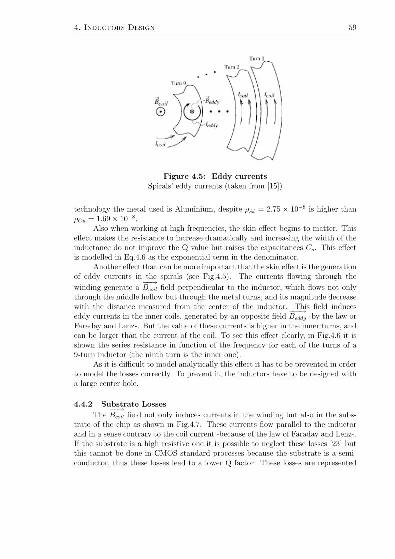
4. Inductors Design 59
Figure 4.5: Eddy currentsSpirals’ eddy currents (taken from [15])
technology the metal used is Aluminium, despite ρAl = 2.75 × 10⁻⁸ is higher thanρCu = 1.69× 10⁻⁸.
Also when working at high frequencies, the skin-effect begins to matter. Thiseffect makes the resistance to increase dramatically and increasing the width of theinductance do not improve the Q value but raises the capacitances Cs. This effectis modelled in Eq.4.6 as the exponential term in the denominator.
Another effect than can be more important that the skin effect is the generationof eddy currents in the spirals (see Fig.4.5). The currents flowing through the
winding generate a−−→Bcoil field perpendicular to the inductor, which flows not only
through the middle hollow but through the metal turns, and its magnitude decreasewith the distance measured from the center of the inductor. This field induceseddy currents in the inner coils, generated by an opposite field
−−−→Beddy -by the law or
Faraday and Lenz-. But the value of these currents is higher in the inner turns, andcan be larger than the current of the coil. To see this effect clearly, in Fig.4.6 it isshown the series resistance in function of the frequency for each of the turns of a9-turn inductor (the ninth turn is the inner one).
As it is difficult to model analytically this effect it has to be prevented in orderto model the losses correctly. To prevent it, the inductors have to be designed witha large center hole.
4.4.2 Substrate Losses
The−−→Bcoil field not only induces currents in the winding but also in the subs-
trate of the chip as shown in Fig.4.7. These currents flow parallel to the inductorand in a sense contrary to the coil current -because of the law of Faraday and Lenz-.If the substrate is a high resistive one it is possible to neglect these losses [23] butthis cannot be done in CMOS standard processes because the substrate is a semi-conductor, thus these losses lead to a lower Q factor. These losses are represented
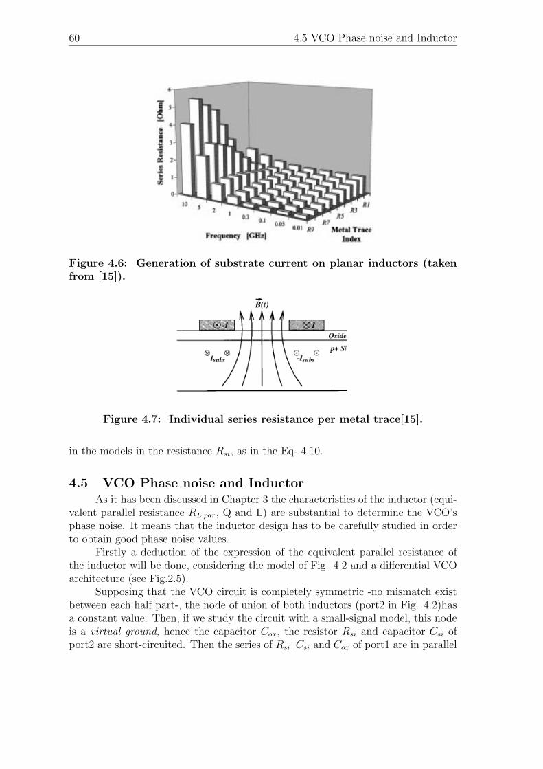
60 4.5 VCO Phase noise and Inductor
Figure 4.6: Generation of substrate current on planar inductors (takenfrom [15]).
Figure 4.7: Individual series resistance per metal trace[15].
in the models in the resistance Rsi, as in the Eq- 4.10.
4.5 VCO Phase noise and InductorAs it has been discussed in Chapter 3 the characteristics of the inductor (equi-
valent parallel resistance RL,par, Q and L) are substantial to determine the VCO’sphase noise. It means that the inductor design has to be carefully studied in orderto obtain good phase noise values.
Firstly a deduction of the expression of the equivalent parallel resistance ofthe inductor will be done, considering the model of Fig. 4.2 and a differential VCOarchitecture (see Fig.2.5).
Supposing that the VCO circuit is completely symmetric -no mismatch existbetween each half part-, the node of union of both inductors (port2 in Fig. 4.2)hasa constant value. Then, if we study the circuit with a small-signal model, this nodeis a virtual ground, hence the capacitor Cox, the resistor Rsi and capacitor Csi ofport2 are short-circuited. Then the series of Rsi‖Csi and Cox of port1 are in parallel

4. Inductors Design 61
Figure 4.8: Conversion of the configuration of Rsi,Csi and Cox into ascheme of a capacitor Csi,ox and a resistance Rsi,ox in parallel.
with the inductor.This series of elements can be modified to be seen as a parallel of a resistance
Rsi,ox and a capacitor Csi,ox as it is depicted in Fig.4.8. For typical values of Rsi, Csi
and Cox the equivalent resistance Rsi,ox is higher than Rsi (the deduction of Rsi,ox
and Csi,ox is in Sec.A.4 of App.A.5).Moreover, the series resistance of the inductor Rs can be transformed into a
parallel resistance by the following equation (see Sec.A.3):
Rs,par = (Q2 + 1) ·Rs∼= Q2 ·Rs
∼=Rs
(Lω0)2(4.13)
Therefore, the equivalent parallel resistance of the inductor is:
RL,par = Rsi,ox‖Rs
(Lω)2(4.14)
For the CMOS standard technologies typically used, Rsi,ox Rs,par, and thenRL,par
∼= Rs,par .These results are used in Sec.3.5 to obtain the phase noise L as a function of
the series resistance of the inductor (refer to Eq.3.37).From what has been observed in this chapter, QL, L or RL,par strongly depend
on the features of the technology used: the metal layers’ number, the inductor’smetal width and the resistance of the substrate. This dependance between theinductor characteristics and the technology result in a direct dependance betweenthe phase noise of the VCO and the technology.
4.6 Simulation toolsThe characteristics of an inductor can be obtained not only by the models
previously mentioned but also utilizing specialized software for this matter.In this work two tools have been used: the freeware ASITIC [53] and the RF
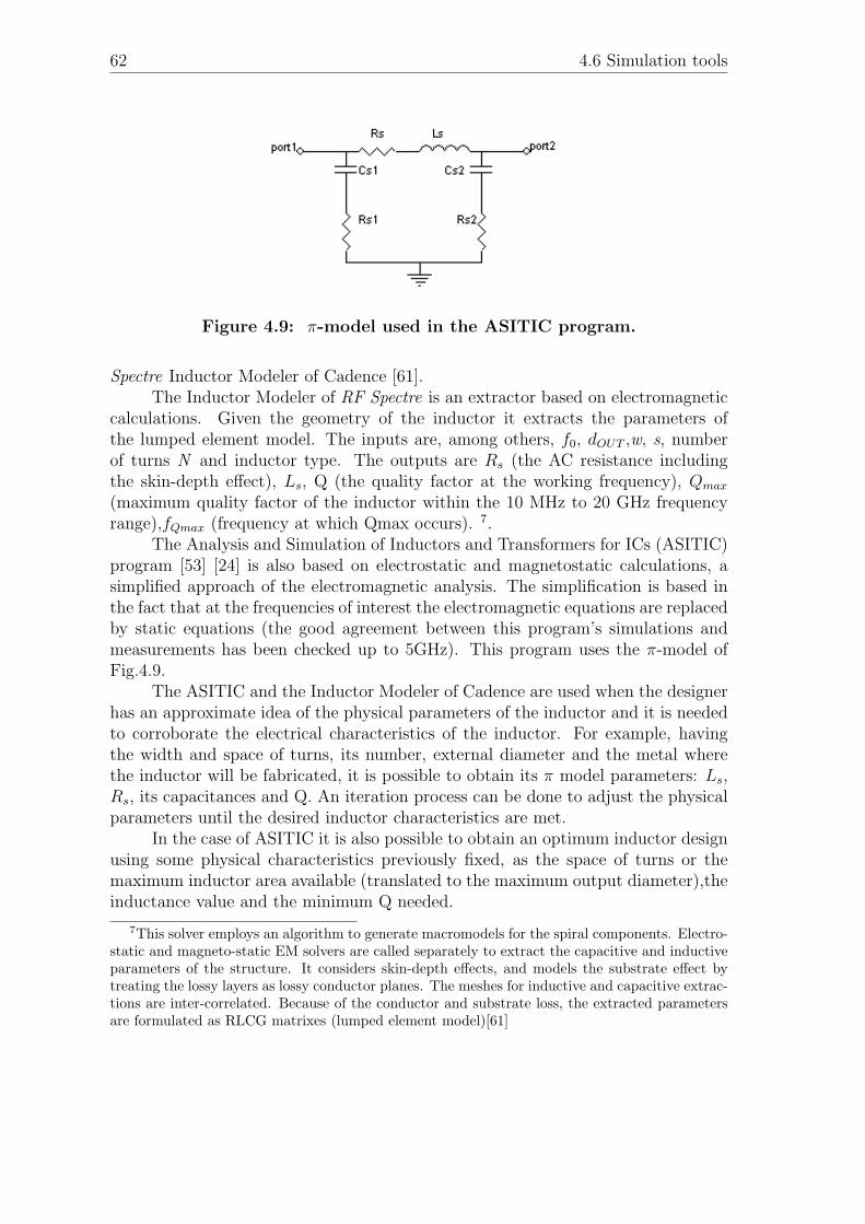
62 4.6 Simulation tools
Figure 4.9: π-model used in the ASITIC program.
Spectre Inductor Modeler of Cadence [61].The Inductor Modeler of RF Spectre is an extractor based on electromagnetic
calculations. Given the geometry of the inductor it extracts the parameters ofthe lumped element model. The inputs are, among others, f0, dOUT ,w, s, numberof turns N and inductor type. The outputs are Rs (the AC resistance includingthe skin-depth effect), Ls, Q (the quality factor at the working frequency), Qmax
(maximum quality factor of the inductor within the 10 MHz to 20 GHz frequencyrange),fQmax (frequency at which Qmax occurs). 7.
The Analysis and Simulation of Inductors and Transformers for ICs (ASITIC)program [53] [24] is also based on electrostatic and magnetostatic calculations, asimplified approach of the electromagnetic analysis. The simplification is based inthe fact that at the frequencies of interest the electromagnetic equations are replacedby static equations (the good agreement between this program’s simulations andmeasurements has been checked up to 5GHz). This program uses the π-model ofFig.4.9.
The ASITIC and the Inductor Modeler of Cadence are used when the designerhas an approximate idea of the physical parameters of the inductor and it is neededto corroborate the electrical characteristics of the inductor. For example, havingthe width and space of turns, its number, external diameter and the metal wherethe inductor will be fabricated, it is possible to obtain its π model parameters: Ls,Rs, its capacitances and Q. An iteration process can be done to adjust the physicalparameters until the desired inductor characteristics are met.
In the case of ASITIC it is also possible to obtain an optimum inductor designusing some physical characteristics previously fixed, as the space of turns or themaximum inductor area available (translated to the maximum output diameter),theinductance value and the minimum Q needed.
7This solver employs an algorithm to generate macromodels for the spiral components. Electro-static and magneto-static EM solvers are called separately to extract the capacitive and inductiveparameters of the structure. It considers skin-depth effects, and models the substrate effect bytreating the lossy layers as lossy conductor planes. The meshes for inductive and capacitive extrac-tions are inter-correlated. Because of the conductor and substrate loss, the extracted parametersare formulated as RLCG matrixes (lumped element model)[61]
4. Inductors Design 63
Some of the advantages of ASITIC are the optimization feature and its speed.On the other hand, as it does not include the effect of substrate in the calculusof inductance; for CMOS technologies it underestimates the substrate losses of theinductor. In the case of RF Spectre modeler, it uses Fasthenry (a program forthe efficient extraction of inductances and resistances of complex 3-D geometries ofconductors [62]), which includes the lossy substrate effect.
In this work, there has been used firstly the ASITIC program to obtain anoptimum design limiting the area; and secondly, to re-check the results from ASITIC,the RF Spectre Modeler. In the following section a deep insight of the design willbe given.
Exampes of others programs which can be utilized for inductor simulation ins-tead of the previously mentioned are: (1) Sonnet (www.sonnetusa.com); (2) SISP -for Windows- (www.elab.ntua.gr/sisp/); (3)HFSS (www.ansoft.com/products/hf/hfss)among others.
4.7 Inductor DesignThe inductor design is bound to the VCO design methodology of Fig.2.8 be-
cause in the VCO’s design flow, the resistance RL,par, the capacitance Cs‖Csi,ox,Q and L values are used to obtain the phase noise, the power consumption andthe transistor sizes, among other VCO’s features. This is why the inductor designmethodology proposed here has two stages. Firstly, using an algorithm which imple-ments the mentioned inductor models, rough values of the inductor characteristicsare obtained and these can be used in the principal routine of the VCO. Secondly,when the final VCO design is chosen, there is an approximate estimation of theL and Q values. With these values, the working frequency and specifications ofgeometrical constrains (spacing between tracks and maximum inductor area), theASITIC feature called optarea can be used to obtain the physical dimensions of theoptimum inductor that obeys these specifications. Later on, using ASITIC or Ca-dence RF Spectre Inductors’ Modeler, an accurate π-model of the designed inductoris calculated, model that is finally re-inserted in the VCO’s design routine to refinethe values of the VCO’s physical parameters.
The VCO finally designed is simulated in Cadence and in this instance it isused the Cadence RF Spectre Inductors’ Modeler. It enables to characterize theinductor designed, being possible to use the model of this inductor in all the stagesof the design in Cadence (schematic, layout and extraction).
The ASITIC program and the RF Spectre Inductors’ Modeler need the physicalcharacteristics of the technology, particularly distances between metals, the metalwidth, the resistivity and the dielectric constant. In our work we use a 0.35µmCMOS technology, which has one poly and 4 metals (the inductors were designed inthe top metal layer for the reasons mentioned in Sec.4.4). The technology processused does not have a very thick top metal, preventing us from improving the Qfactor of the inductor. In Fig.4.10 is a scheme of the layers of this technology andin Fig. 4.11 it is shown graphically data that needs both software tools.
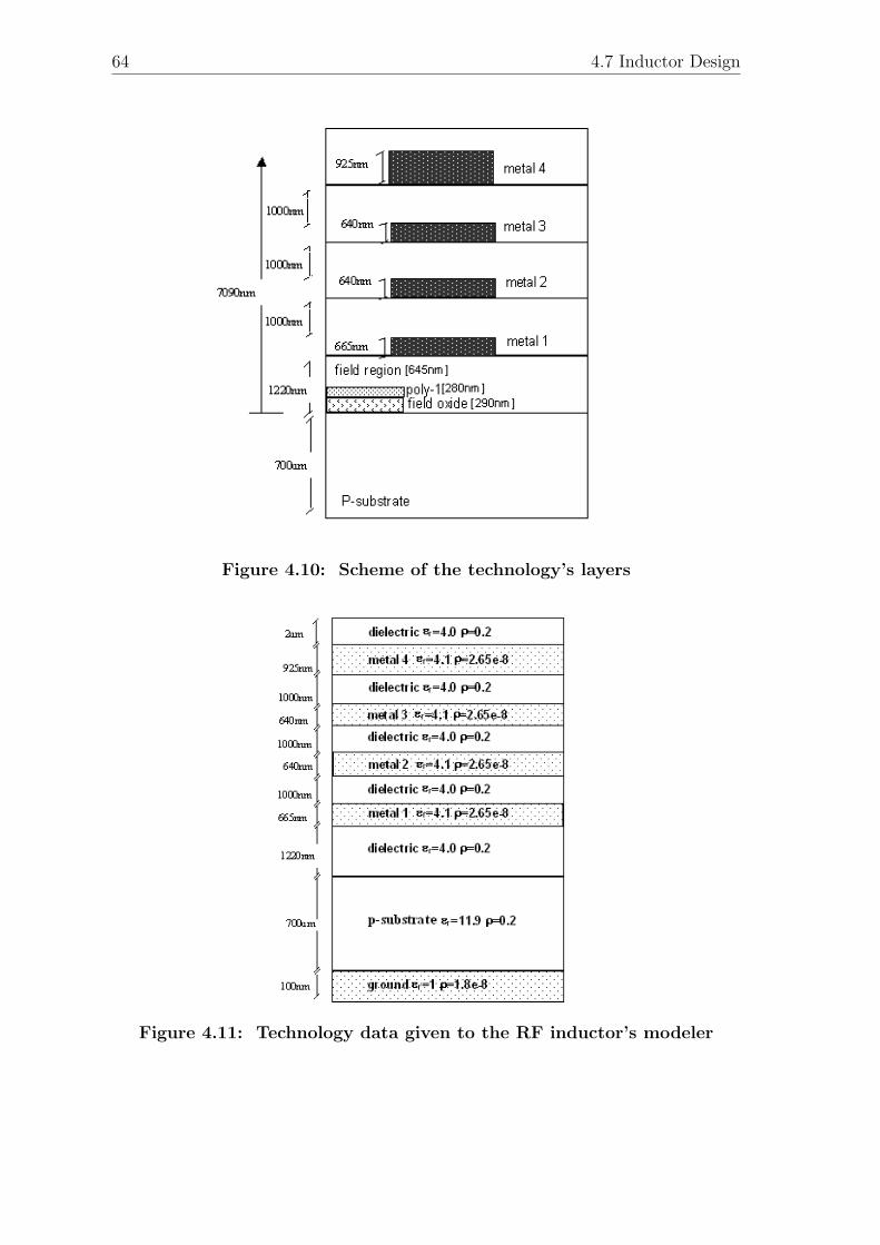
64 4.7 Inductor Design
Figure 4.10: Scheme of the technology’s layers
Figure 4.11: Technology data given to the RF inductor’s modeler

4. Inductors Design 65
Figure 4.12: Final layout design of the inductor
The function optarea of ASITIC has as inputs the geometry, the workingfrequency, the inductor metal, a fixed spacing, the L value and its accuracy, a rangeof width track, a range of output diameter and a minimum Q. Its output are thetrace width w, the output diameter dout and the number of turns. The resultinginductor , for L = 5nH, f0 = 915MHz, s = 1.5µm and Qmin ≈ 3 are given in Table4.2 (see Fig.4.12):
Geometry squareMetal top metal
Number of turns 4w(µ m) 14s(µ m) 1.5dout(µ m) 260
Table 4.2: Geometric parameters obtained with the function optarea ofASITIC
With these inductor dimensions, it has been obtained the electrical parametersusing various methods.
Using the equations of Yue’s Model and the expression of Mohan’s inductance
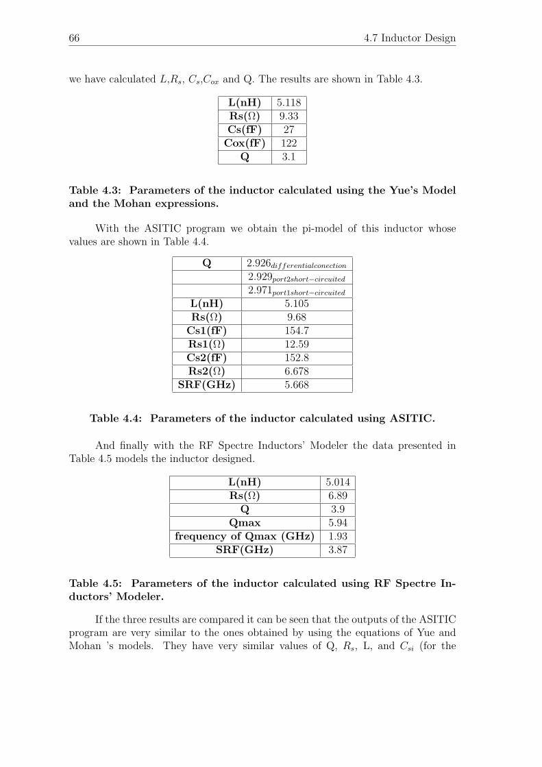
66 4.7 Inductor Design
we have calculated L,Rs, Cs,Cox and Q. The results are shown in Table 4.3.
L(nH) 5.118Rs(Ω) 9.33Cs(fF) 27Cox(fF) 122
Q 3.1
Table 4.3: Parameters of the inductor calculated using the Yue’s Modeland the Mohan expressions.
With the ASITIC program we obtain the pi-model of this inductor whosevalues are shown in Table 4.4.
Q 2.926differentialconection
2.929port2short−circuited
2.971port1short−circuited
L(nH) 5.105Rs(Ω) 9.68
Cs1(fF) 154.7Rs1(Ω) 12.59Cs2(fF) 152.8Rs2(Ω) 6.678
SRF(GHz) 5.668
Table 4.4: Parameters of the inductor calculated using ASITIC.
And finally with the RF Spectre Inductors’ Modeler the data presented inTable 4.5 models the inductor designed.
L(nH) 5.014Rs(Ω) 6.89
Q 3.9Qmax 5.94
frequency of Qmax (GHz) 1.93SRF(GHz) 3.87
Table 4.5: Parameters of the inductor calculated using RF Spectre In-ductors’ Modeler.
If the three results are compared it can be seen that the outputs of the ASITICprogram are very similar to the ones obtained by using the equations of Yue andMohan ’s models. They have very similar values of Q, Rs, L, and Csi (for the

4. Inductors Design 67
equivalence between the π model of ASITIC and model used in Yue’s equationscompare the Figs.4.2 and 4.9).
In the results obtained by Cadence tool, the inductance value is very similarto the other two models but there is a slight difference in the quality factor and inthe series resistance. The difference is about 20% approximately in the Q factor an25% in the series resistance factor.
It was expected that the Q factor obtained with the Cadence tool might belower because it considers the losses of the substrate. But the documentation of thattool has not sufficient information to understand why this happens. Therefore wedecide to use the data of the ASITIC program because it was clearly documentedand we know clearly which are its problems.

68
Chapter 5Varactor Design
5.1 IntroductionTowards the application of CMOS technologies in radio-frequencies, not only
the attention has been put in the monolithic inductor but also in improving thevaractors. They are capacitors which can tune its capacitance value by means ofa bias voltage. They are not passive devices as they are made using active devicessuch as diodes or transistors.
In most cases the quality factor of the varactor Qvar is high enough comparedto the quality factor of the inductor to neglect the non-idealities. Anyway thesedevices have to be studied in order to check this assumption. In the last years it hasbeen an improvement in the varactor topologies to increase the Qvar as it is shownin [63][14].
The aim of this chapter is to show the most common varactors’ topologies, tostudy more deeply the varactor topology utilized in the final design and to discussthe final layout.
5.2 Varactors topologiesThe topologies of varactors widely used are:
• p-n reverse biased diode
• MOS varactors:
1. Drain-Source-Bulk structure (D-S-B MOS).
2. Inversion-mode MOS (I-MOS)
3. Accumulation-mode MOS (A-MOS)
p-n reverse biased diode
The first topology is a basic structure used in VCOs [18]: a reverse biased diodeused as a capacitor. Its simplified electrical model and symbol are shown in Fig.5.1[64]. This simplified model does not consider the inductance in series with the capa-citance. The capacitance Cj is the reverse p-n junction capacitance, RV ar,series is theseries parasitic resistance and RV ar,par is the parallel resistance due to the substratelosses. The capacitance can be varied because Cj has a dependence on the reversebias voltage Vrev of the p-n junction given by Eq.5.1:
Cj = Cj0
( V0
V0 + Vrev
)m
(5.1)
69
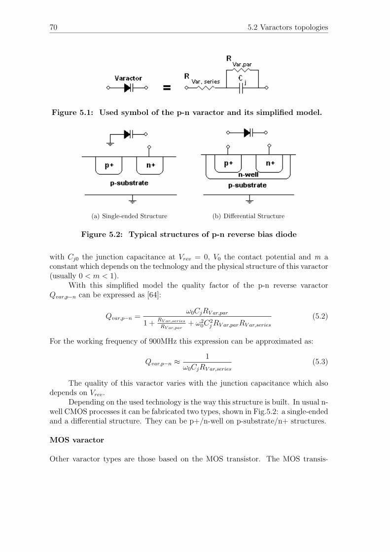
70 5.2 Varactors topologies
Figure 5.1: Used symbol of the p-n varactor and its simplified model.
(a) Single-ended Structure (b) Differential Structure
Figure 5.2: Typical structures of p-n reverse bias diode
with Cj0 the junction capacitance at Vrev = 0, V0 the contact potential and m aconstant which depends on the technology and the physical structure of this varactor(usually 0 < m < 1).
With this simplified model the quality factor of the p-n reverse varactorQvar,p−n can be expressed as [64]:
Qvar,p−n =ω0CjRV ar,par
1 +RV ar,series
RV ar,par+ ω2
0C2jRV ar,parRV ar,series
(5.2)
For the working frequency of 900MHz this expression can be approximated as:
Qvar,p−n ≈1
ω0CjRV ar,series
(5.3)
The quality of this varactor varies with the junction capacitance which alsodepends on Vrev.
Depending on the used technology is the way this structure is built. In usual n-well CMOS processes it can be fabricated two types, shown in Fig.5.2: a single-endedand a differential structure. They can be p+/n-well on p-substrate/n+ structures.
MOS varactor
Other varactor types are those based on the MOS transistor. The MOS transis-
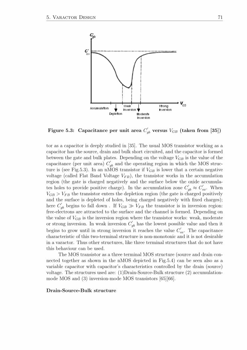
5. Varactor Design 71
Figure 5.3: Capacitance per unit area C′
gb versus VGB (taken from [35])
tor as a capacitor is deeply studied in [35]. The usual MOS transistor working as acapacitor has the source, drain and bulk short circuited, and the capacitor is formedbetween the gate and bulk plates. Depending on the voltage VGB is the value of thecapacitance (per unit area) C
′
gb and the operating region in which the MOS struc-ture is (see Fig.5.3). In an nMOS transistor if VGB is lower that a certain negativevoltage (called Flat Band Voltage VFB), the transistor works in the accumulationregion (the gate is charged negatively and the surface below the oxide accumula-tes holes to provide positive charge). In the accumulation zone C
′
gb ≈ C′ox. When
VGB > VFB the transistor enters the depletion region (the gate is charged positivelyand the surface is depleted of holes, being charged negatively with fixed charges);here C
′
gb begins to fall down . If VGB VFB the transistor is in inversion region:free-electrons are attracted to the surface and the channel is formed. Depending onthe value of VGB is the inversion region where the transistor works: weak, moderateor strong inversion. In weak inversion C
′
gb has the lowest possible value and then it
begins to grow until in strong inversion it reaches the value C′ox. The capacitance
characteristic of this two-terminal structure is non-monotonic and it is not desirablein a varactor. Thus other structures, like three terminal structures that do not havethis behaviour can be used.
The MOS transistor as a three terminal MOS structure (source and drain con-nected together as shown in the nMOS depicted in Fig.5.4) can be seen also as avariable capacitor with capacitor’s characteristics controlled by the drain (source)voltage. The structures used are: (1)Drain-Source-Bulk structure (2) accumulation-mode MOS and (3) inversion-mode MOS transistors [65][66].
Drain-Source-Bulk structure
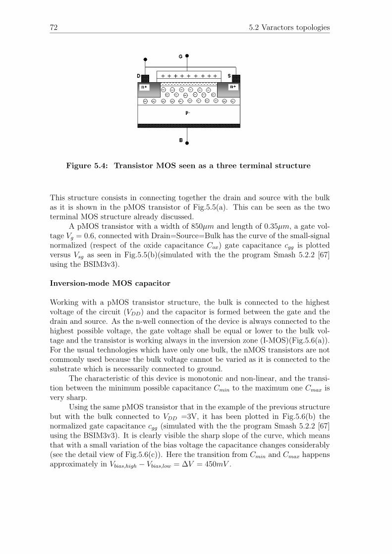
72 5.2 Varactors topologies
Figure 5.4: Transistor MOS seen as a three terminal structure
This structure consists in connecting together the drain and source with the bulkas it is shown in the pMOS transistor of Fig.5.5(a). This can be seen as the twoterminal MOS structure already discussed.
A pMOS transistor with a width of 850µm and length of 0.35µm, a gate vol-tage Vg = 0.6, connected with Drain=Source=Bulk has the curve of the small-signalnormalized (respect of the oxide capacitance Cox) gate capacitance cgg is plottedversus Vsg as seen in Fig.5.5(b)(simulated with the the program Smash 5.2.2 [67]using the BSIM3v3).
Inversion-mode MOS capacitor
Working with a pMOS transistor structure, the bulk is connected to the highestvoltage of the circuit (VDD) and the capacitor is formed between the gate and thedrain and source. As the n-well connection of the device is always connected to thehighest possible voltage, the gate voltage shall be equal or lower to the bulk vol-tage and the transistor is working always in the inversion zone (I-MOS)(Fig.5.6(a)).For the usual technologies which have only one bulk, the nMOS transistors are notcommonly used because the bulk voltage cannot be varied as it is connected to thesubstrate which is necessarily connected to ground.
The characteristic of this device is monotonic and non-linear, and the transi-tion between the minimum possible capacitance Cmin to the maximum one Cmax isvery sharp.
Using the same pMOS transistor that in the example of the previous structurebut with the bulk connected to VDD =3V, it has been plotted in Fig.5.6(b) thenormalized gate capacitance cgg (simulated with the the program Smash 5.2.2 [67]using the BSIM3v3). It is clearly visible the sharp slope of the curve, which meansthat with a small variation of the bias voltage the capacitance changes considerably(see the detail view of Fig.5.6(c)). Here the transition from Cmin and Cmax happensapproximately in Vbias,high − Vbias,low = ∆V = 450mV .
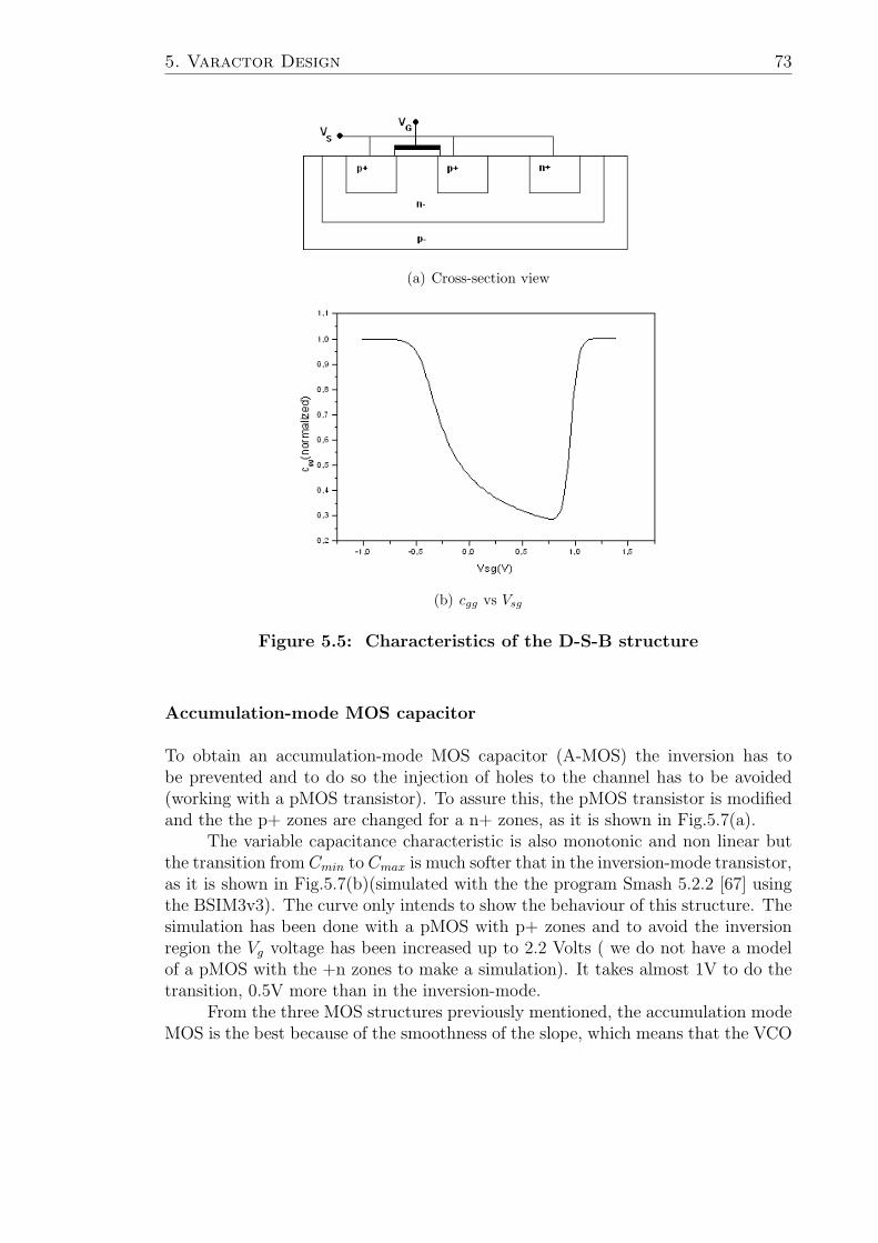
5. Varactor Design 73
(a) Cross-section view
(b) cgg vs Vsg
Figure 5.5: Characteristics of the D-S-B structure
Accumulation-mode MOS capacitor
To obtain an accumulation-mode MOS capacitor (A-MOS) the inversion has tobe prevented and to do so the injection of holes to the channel has to be avoided(working with a pMOS transistor). To assure this, the pMOS transistor is modifiedand the the p+ zones are changed for a n+ zones, as it is shown in Fig.5.7(a).
The variable capacitance characteristic is also monotonic and non linear butthe transition from Cmin to Cmax is much softer that in the inversion-mode transistor,as it is shown in Fig.5.7(b)(simulated with the the program Smash 5.2.2 [67] usingthe BSIM3v3). The curve only intends to show the behaviour of this structure. Thesimulation has been done with a pMOS with p+ zones and to avoid the inversionregion the Vg voltage has been increased up to 2.2 Volts ( we do not have a modelof a pMOS with the +n zones to make a simulation). It takes almost 1V to do thetransition, 0.5V more than in the inversion-mode.
From the three MOS structures previously mentioned, the accumulation modeMOS is the best because of the smoothness of the slope, which means that the VCO
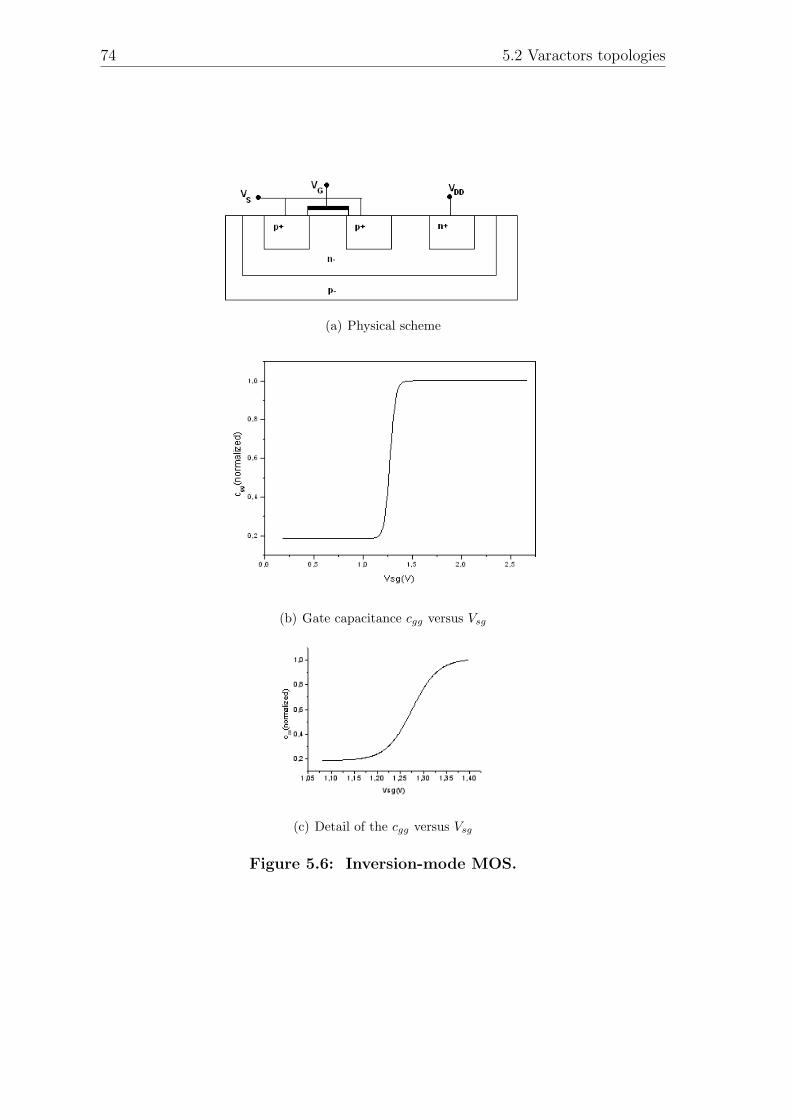
74 5.2 Varactors topologies
(a) Physical scheme
(b) Gate capacitance cgg versus Vsg
(c) Detail of the cgg versus Vsg
Figure 5.6: Inversion-mode MOS.
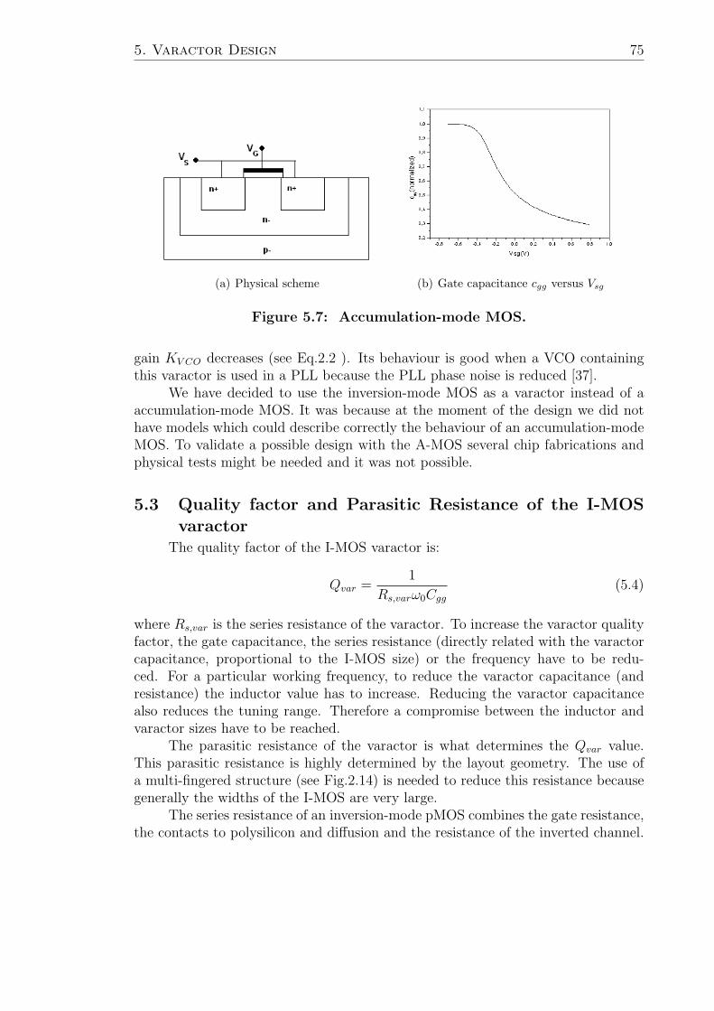
5. Varactor Design 75
(a) Physical scheme (b) Gate capacitance cgg versus Vsg
Figure 5.7: Accumulation-mode MOS.
gain KV CO decreases (see Eq.2.2 ). Its behaviour is good when a VCO containingthis varactor is used in a PLL because the PLL phase noise is reduced [37].
We have decided to use the inversion-mode MOS as a varactor instead of aaccumulation-mode MOS. It was because at the moment of the design we did nothave models which could describe correctly the behaviour of an accumulation-modeMOS. To validate a possible design with the A-MOS several chip fabrications andphysical tests might be needed and it was not possible.
5.3 Quality factor and Parasitic Resistance of the I-MOSvaractor
The quality factor of the I-MOS varactor is:
Qvar =1
Rs,varω0Cgg
(5.4)
where Rs,var is the series resistance of the varactor. To increase the varactor qualityfactor, the gate capacitance, the series resistance (directly related with the varactorcapacitance, proportional to the I-MOS size) or the frequency have to be redu-ced. For a particular working frequency, to reduce the varactor capacitance (andresistance) the inductor value has to increase. Reducing the varactor capacitancealso reduces the tuning range. Therefore a compromise between the inductor andvaractor sizes have to be reached.
The parasitic resistance of the varactor is what determines the Qvar value.This parasitic resistance is highly determined by the layout geometry. The use ofa multi-fingered structure (see Fig.2.14) is needed to reduce this resistance becausegenerally the widths of the I-MOS are very large.
The series resistance of an inversion-mode pMOS combines the gate resistance,the contacts to polysilicon and diffusion and the resistance of the inverted channel.
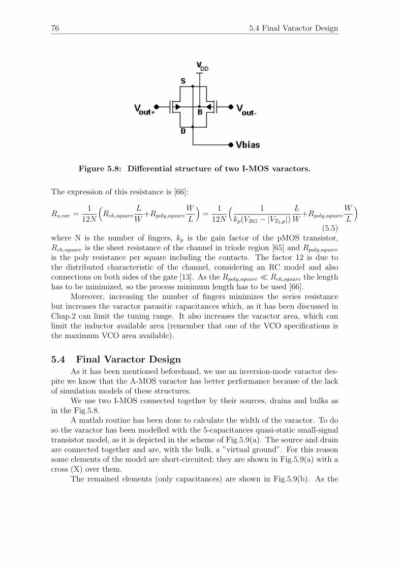
76 5.4 Final Varactor Design
Figure 5.8: Differential structure of two I-MOS varactors.
The expression of this resistance is [66]:
Rs,var =1
12N
(Rch,square
L
W+Rpoly,square
W
L
)=
1
12N
( 1
kp(VBG − |VT0,p|)L
W+Rpoly,square
W
L
)(5.5)
where N is the number of fingers, kp is the gain factor of the pMOS transistor,Rch,square is the sheet resistance of the channel in triode region [65] and Rpoly,square
is the poly resistance per square including the contacts. The factor 12 is due tothe distributed characteristic of the channel, considering an RC model and alsoconnections on both sides of the gate [13]. As the Rpoly,square Rch,square the lengthhas to be minimized, so the process minimum length has to be used [66].
Moreover, increasing the number of fingers minimizes the series resistancebut increases the varactor parasitic capacitances which, as it has been discussed inChap.2 can limit the tuning range. It also increases the varactor area, which canlimit the inductor available area (remember that one of the VCO specifications isthe maximum VCO area available).
5.4 Final Varactor DesignAs it has been mentioned beforehand, we use an inversion-mode varactor des-
pite we know that the A-MOS varactor has better performance because of the lackof simulation models of these structures.
We use two I-MOS connected together by their sources, drains and bulks asin the Fig.5.8.
A matlab routine has been done to calculate the width of the varactor. To doso the varactor has been modelled with the 5-capacitances quasi-static small-signaltransistor model, as it is depicted in the scheme of Fig.5.9(a). The source and drainare connected together and are, with the bulk, a ”virtual ground”. For this reasonsome elements of the model are short-circuited; they are shown in Fig.5.9(a) with across (X) over them.
The remained elements (only capacitances) are shown in Fig.5.9(b). As the
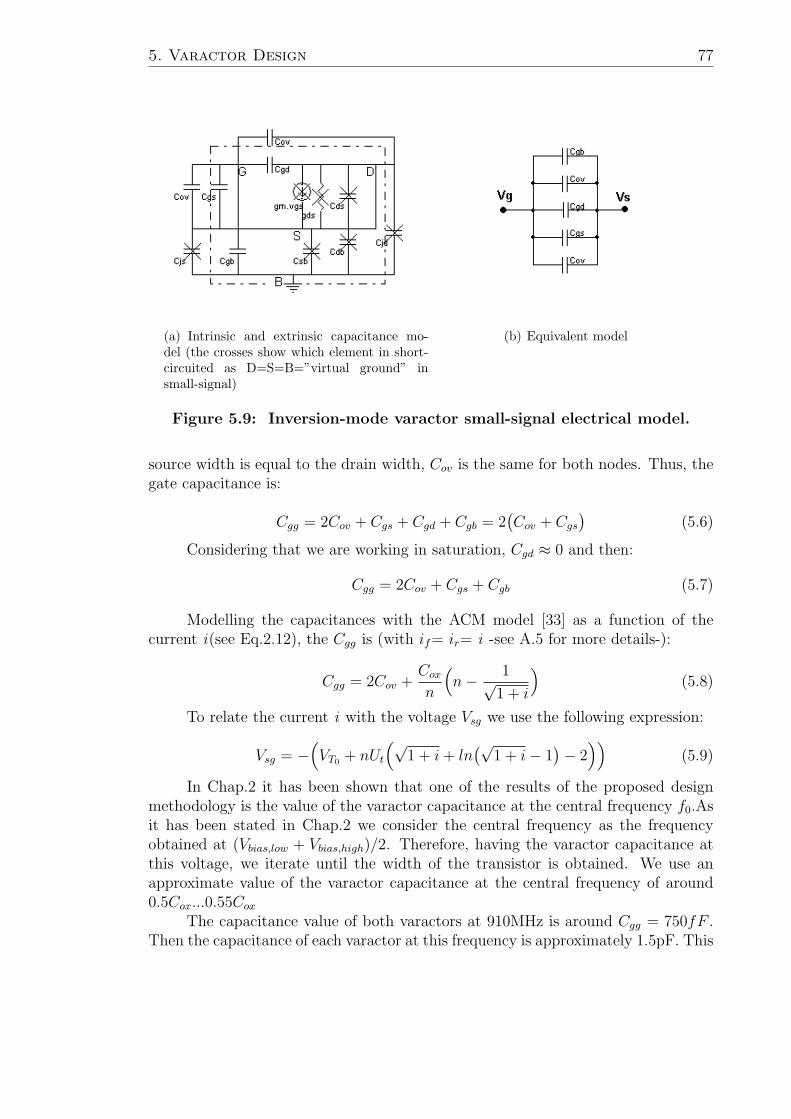
5. Varactor Design 77
(a) Intrinsic and extrinsic capacitance mo-del (the crosses show which element in short-circuited as D=S=B=”virtual ground” insmall-signal)
(b) Equivalent model
Figure 5.9: Inversion-mode varactor small-signal electrical model.
source width is equal to the drain width, Cov is the same for both nodes. Thus, thegate capacitance is:
Cgg = 2Cov + Cgs + Cgd + Cgb = 2(Cov + Cgs
)(5.6)
Considering that we are working in saturation, Cgd ≈ 0 and then:
Cgg = 2Cov + Cgs + Cgb (5.7)
Modelling the capacitances with the ACM model [33] as a function of thecurrent i(see Eq.2.12), the Cgg is (with if= ir= i -see A.5 for more details-):
Cgg = 2Cov +Cox
n
(n− 1√
1 + i
)(5.8)
To relate the current i with the voltage Vsg we use the following expression:
Vsg = −(VT0 + nUt
(√1 + i+ ln
(√1 + i− 1
)− 2
))(5.9)
In Chap.2 it has been shown that one of the results of the proposed designmethodology is the value of the varactor capacitance at the central frequency f0.Asit has been stated in Chap.2 we consider the central frequency as the frequencyobtained at (Vbias,low + Vbias,high)/2. Therefore, having the varactor capacitance atthis voltage, we iterate until the width of the transistor is obtained. We use anapproximate value of the varactor capacitance at the central frequency of around0.5Cox...0.55Cox
The capacitance value of both varactors at 910MHz is around Cgg = 750fF .Then the capacitance of each varactor at this frequency is approximately 1.5pF. This
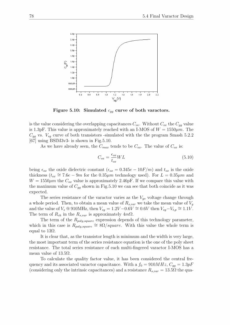
78 5.4 Final Varactor Design
Figure 5.10: Simulated cgg curve of both varactors.
is the value considering the overlapping capacitances Cov. Without Cov the Cgg valueis 1.3pF. This value is approximately reached with an I-MOS of W = 1550µm. TheCgg vs. Vsg curve of both transistors -simulated with the the program Smash 5.2.2[67] using BSIM3v3- is shown in Fig.5.10.
As we have already seen, the Cmax tends to be Cox. The value of Cox is:
Cox =εox
tox
WL (5.10)
being εox the oxide dielectric constant (εox = 0.345e− 10F/m) and tox is the oxidethickness (tox
∼= 7.6e − 9m for the 0.35µm technology used). For L = 0.35µm andW = 1550µm the Cox value is approximately 2.46pF. If we compare this value withthe maximum value of Cgg shown in Fig.5.10 we can see that both coincide as it wasexpected.
The series resistance of the varactor varies as the Vgs voltage change througha whole period. Then, to obtain a mean value of Rs,var we take the mean value of Vg
and the value of Vs @ 910MHz, then Vsg = 1.2V−0.6V ∼= 0.6V then Vsg−Vt,p∼= 1.1V .
The term of Rch in the Rs,var is approximately 4mΩ.The term of the Rpoly,square expression depends of this technology parameter,
which in this case is Rpoly,square∼= 8Ω/square. With this value the whole term is
equal to 13Ω.It is clear that, as the transistor length is minimum and the width is very large,
the most important term of the series resistance equation is the one of the poly sheetresistance. The total series resistance of each multi-fingered varactor I-MOS has amean value of 13.5Ω.
To calculate the quality factor value, it has been considered the central fre-quency and its associated varactor capacitance. With a f0 = 910MHz, Cgg = 1.3pF(considering only the intrinsic capacitances) and a resistance Rs,var = 13.5Ω the qua-
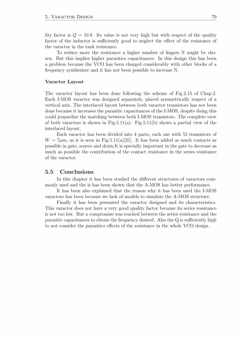
5. Varactor Design 79
lity factor is Q = 10.9. Its value is not very high but with respect of the qualityfactor of the inductor is sufficiently good to neglect the effect of the resistance ofthe varactor in the tank resistance.
To reduce more the resistance a higher number of fingers N might be cho-sen. But this implies higher parasitics capacitances. In this design this has beena problem because the VCO has been charged considerably with other blocks of afrequency synthesizer and it has not been possible to increase N.
Varactor Layout
The varactor layout has been done following the scheme of Fig.2.15 of Chap.2.Each I-MOS varactor was designed separately, placed symmetrically respect of avertical axis. The interlaced layout between both varactor transistors has not beendone because it increases the parasitic capacitances of the I-MOS, despite doing thiscould jeopardize the matching between both I-MOS transistors. The complete viewof both varactors is shown in Fig.5.11(a). Fig.5.11(b) shows a partial view of theinterlaced layout.
Each varactor has been divided into 4 parts, each one with 55 transistors ofW = 7µm, as it is seen in Fig.5.11(a)[31]. It has been added as much contacts aspossible in gate, source and drain.It is specially important in the gate to decrease asmuch as possible the contribution of the contact resistance in the series resistanceof the varactor.
5.5 ConclusionsIn this chapter it has been studied the different structures of varactors com-
monly used and the is has been shown that the A-MOS has better performance.It has been also explained that the reason why it has been used the I-MOS
varactors has been because we lack of models to simulate the A-MOS structure.Finally it has been presented the varactor designed and its characteristics.
This varactor does not have a very good quality factor because its series resistanceis not too low. But a compromise was reached between the series resistance and theparasitic capacitances to obtain the frequency desired. Also the Q is sufficiently highto not consider the parasitics effects of the resistance in the whole VCO design.
80 5.5 Conclusions
(a) Complete view
(b) Partial view
Figure 5.11: Varactor Layout
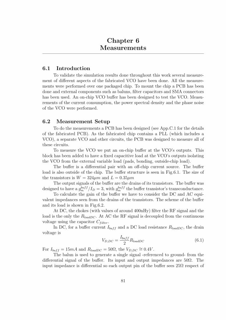
Chapter 6Measurements
6.1 IntroductionTo validate the simulation results done throughout this work several measure-
ment of different aspects of the fabricated VCO have been done. All the measure-ments were performed over one packaged chip. To mount the chip a PCB has beendone and external components such as baluns, filter capacitors and SMA connectorshas been used. An on-chip VCO buffer has been designed to test the VCO. Measu-rements of the current consumption, the power spectral density and the phase noiseof the VCO were performed.
6.2 Measurement SetupTo do the measurements a PCB has been designed (see App.C.1 for the details
of the fabricated PCB). As the fabricated chip contains a PLL (which includes aVCO), a separate VCO and other circuits, the PCB was designed to measure all ofthese circuits.
To measure the VCO we put an on-chip buffer at the VCO’s outputs. Thisblock has been added to have a fixed capacitive load at the VCO’s outputs isolatingthe VCO from the external variable load (pads, bonding, outside-chip load).
The buffer is a differential pair with an off-chip current source. The bufferload is also outside of the chip. The buffer structure is seen in Fig.6.1. The size ofthe transistors is W = 324µm and L = 0.35µm
The output signals of the buffer are the drains of its transistors. The buffer wasdesigned to have a gbuff
m /ID = 3, with gbuffm the buffer transistor’s transconductance.
To calculate the gain of the buffer we have to consider the DC and AC equi-valent impedances seen from the drains of the transistors. The scheme of the bufferand its load is shown in Fig.6.2.
At DC, the chokes (with values of around 400nHy) filter the RF signal and theload is the only the RloadDC . At AC the RF signal is decoupled from the continuousvoltage using the capacitor Cfilter.
In DC, for a buffer current Ibuff and a DC load resistance RloadDC , the drainvoltage is
VD,DC =Ibuff
2RloadDC (6.1)
For Ibuff = 15mA and RloadDC = 50Ω, the VD,DC∼= 0.4V .
The balun is used to generate a single signal -referenced to ground- from thedifferential signal of the buffer. Its input and output impedances are 50Ω. Theinput impedance is differential so each output pin of the buffer sees 25Ω respect of
81
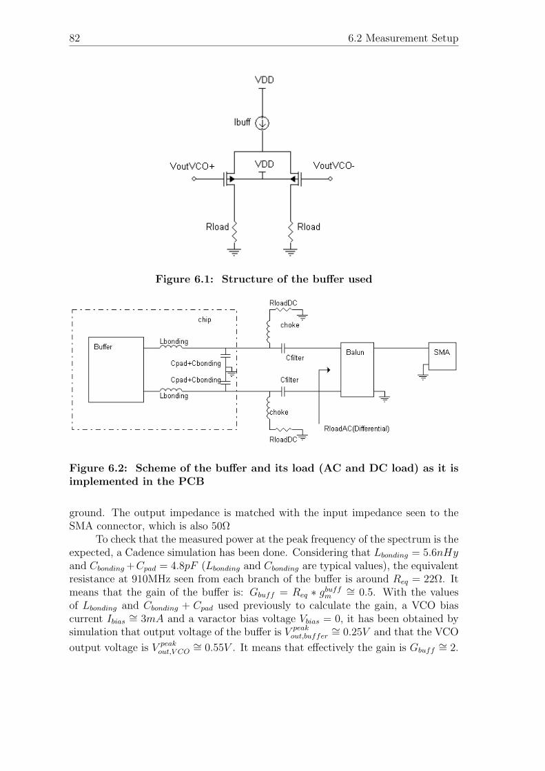
82 6.2 Measurement Setup
Figure 6.1: Structure of the buffer used
Figure 6.2: Scheme of the buffer and its load (AC and DC load) as it isimplemented in the PCB
ground. The output impedance is matched with the input impedance seen to theSMA connector, which is also 50Ω
To check that the measured power at the peak frequency of the spectrum is theexpected, a Cadence simulation has been done. Considering that Lbonding = 5.6nHyand Cbonding +Cpad = 4.8pF (Lbonding and Cbonding are typical values), the equivalentresistance at 910MHz seen from each branch of the buffer is around Req = 22Ω. Itmeans that the gain of the buffer is: Gbuff = Req ∗ gbuff
m∼= 0.5. With the values
of Lbonding and Cbonding + Cpad used previously to calculate the gain, a VCO biascurrent Ibias
∼= 3mA and a varactor bias voltage Vbias = 0, it has been obtained bysimulation that output voltage of the buffer is V peak
out,buffer∼= 0.25V and that the VCO
output voltage is V peakout,V CO
∼= 0.55V . It means that effectively the gain is Gbuff∼= 2.
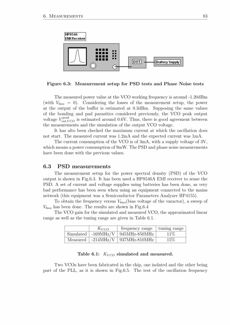
6. Measurements 83
Figure 6.3: Measurement setup for PSD tests and Phase Noise tests
The measured power value at the VCO working frequency is around -1.20dBm(with Vbias = 0). Considering the losses of the measurement setup, the powerat the output of the buffer is estimated at 0.3dBm. Supposing the same valuesof the bonding and pad parasitics considered previously, the VCO peak outputvoltage V peak
out,V CO is estimated around 0.6V. Thus, there is good agreement betweenthe measurements and the simulation of the output VCO voltage.
It has alto been checked the maximum current at which the oscillation doesnot start. The measured current was 1.2mA and the expected current was 1mA.
The current consumption of the VCO is of 3mA, with a supply voltage of 3V,which means a power consumption of 9mW. The PSD and phase noise measurementshave been done with the previous values.
6.3 PSD measurementsThe measurement setup for the power spectral density (PSD) of the VCO
output is shown in Fig.6.3. It has been used a HP8546A EMI receiver to sense thePSD. A set of current and voltage supplies using batteries has been done, as verybad performance has been seen when using an equipment connected to the mainsnetwork (this equipment was a Semiconductor Parameters Analyzer HP4155).
To obtain the frequency versus Vbias(bias voltage of the varactor), a sweep ofVbias has been done. The results are shown in Fig.6.4
The VCO gain for the simulated and measured VCO, the approximated linearrange as well as the tuning range are given in Table 6.1.
KV CO frequency range tuning rangeSimulated -169MHz/V 945MHz-850MHz 11%Measured -214MHz/V 937MHz-810MHz 15%
Table 6.1: KV CO simulated and measured.
Two VCOs have been fabricated in the chip, one isolated and the other beingpart of the PLL, as it is shown in Fig.6.5. The test of the oscillation frequency

84 6.4 Phase noise measurements
Figure 6.4: VCO oscillation frequency versus Vbias
versus Vbias was done with the isolated VCO. The study of the power spectrum ofthe signal has been done with the PLL’s VCO. Some differences were encounteredspecially in the frequency range. The highest frequency of the VCO belonging tothe PLL was approximately 25MHZ lower respect of the isolated one. It is expectedas the former has more capacitive load.
The output spectrum of the signal with Vbias = 0 is the one shown in Fig.6.6.
6.4 Phase noise measurementsAs we do not have any equipment to measure the phase noise of the signal,
we use the same setup as in the PSD measurement. We apply the definition of thephase noise (refer to Eq.3.3) to obtain a set of results.
We measure it at different frequency offsets from the carrier. The bandwidthused was 30Hz instead on 1Hz as it is stated in the definition, but we consideredthat no appreciable difference will be measured ( 30Hz is the smallest bandwidth ofthe equipment used). At Table 6.2 the values of the phase noise measured are given.
∆f from the carrier phase noise measured (dBc/Hz)100kHz -87600kHz -1021MHz -107
Table 6.2: Phase noise measured at VDD = 3V and Ibias = 3mA
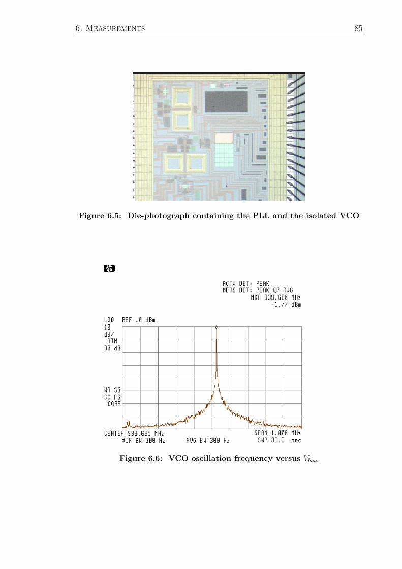
6. Measurements 85
Figure 6.5: Die-photograph containing the PLL and the isolated VCO
Figure 6.6: VCO oscillation frequency versus Vbias
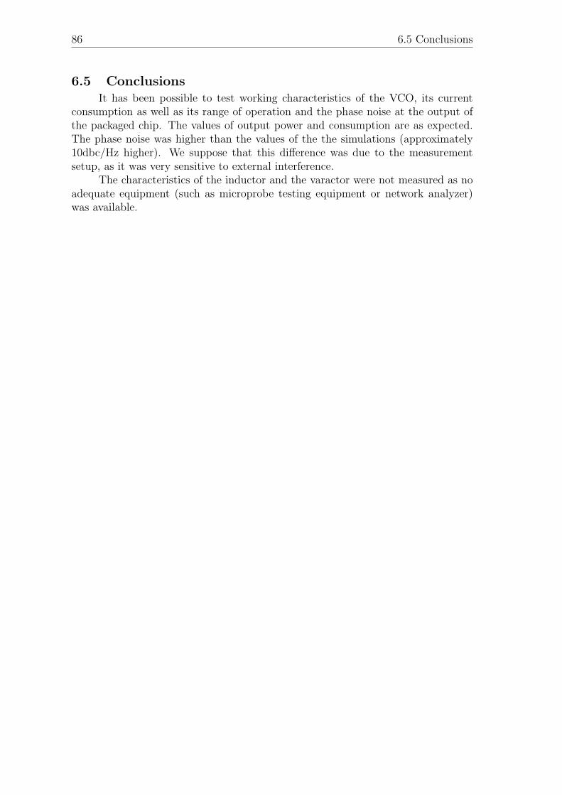
86 6.5 Conclusions
6.5 ConclusionsIt has been possible to test working characteristics of the VCO, its current
consumption as well as its range of operation and the phase noise at the output ofthe packaged chip. The values of output power and consumption are as expected.The phase noise was higher than the values of the the simulations (approximately10dbc/Hz higher). We suppose that this difference was due to the measurementsetup, as it was very sensitive to external interference.
The characteristics of the inductor and the varactor were not measured as noadequate equipment (such as microprobe testing equipment or network analyzer)was available.
Chapter 7Conclusions and Future Work
7.1 IntroductionIn this chapter the challenges of designing a fully integrated VCO as well as the
key features of the designed VCO and its possible improvements are discussed. Abrief discussion about designing in moderate inversion is given as well as commentsabout the design methodology proposed. A conclusion is drawn and future work onthis subject is also included.
7.2 Challenges of designing an on-chip low power VCOThere are several difficulties in designing low power on-chip VCOs with good
performance. As we have already mentioned, the phase noise is a very importantfeature of the VCO because high phase noise jeopardizes the reception and trans-mission of a signal. But the way to decrease the phase noise is increasing the biascurrent of the circuit. So a trade-off between the consumption of the circuit and thephase noise generated must be found.
The on-chip VCO is a feature of the circuit that has pros and cons. Thefact that the VCO is in a chip makes a design more compact and robust. But asmonolithic inductors are used the VCO quality factor is reduced considerably. On-chip inductors in CMOS standard technology have Q ∼= 3..5 while off-chip inductorscan have quality factors of 40 [12]. However improvements have been done [15][24][68] to increase the inductor low-quality-factor.
The inductor value also fixes the phase noise. If the quality factor of theinductor is not constant (as generally occurs) and the inductor value is raised thephase noise rises too, although this increment is small.
The inductor highly determines the VCO current consumption. In CMOStechnologies the on-chip inductors have low quality factor values so the currentconsumption rises respect of a high quality inductor. The VCO transistors’ gm isproportional either to the bias current and to the inductor conductance(refers toEq.2.15). It means that a low quality inductor has a higher conductance than ahigh quality one and then the current consumption is also higher.
The MOS varactor might modify the characteristics of the VCO, specially ifthe width of it is large enough to deteriorate its quality factor. In this component isspecially important doing a multi-fingered layout, and choose correctly the numberof fingers.
The parasitic capacitances of the layout cannot be neglected, specially workingin moderate inversion region. In this region the width of the transistors can besufficiently high so that the overlap and junction capacitances cannot be neglected.
87
88 7.3 Key features of the proposed VCO
If a careless layout is done and all the parasitics are not taken into account, the VCOworking frequency shall drop dozens of megahertz below the expected frequency oreven more.
The current source is also an important block of the VCO. Its noise is upcon-verted by the cross-coupled block and it increases the VCO phase noise. By choosinga pMOS current source with very big transistors makes decrease the injected noiseto the VCO.
7.3 Key features of the proposed VCOThe VCO designed has a current consumption of 3mA, a measured phase noise
of -107dBc/Hz @1MHz, a tuning range of 15% for a 3V supply and an area of 500µmby 600µm. These values are under the initial specifications of the VCO.
The minimum current at which the VCO oscillates was measured to be 1.2mA,and very good correlation exists between this value and the one expected fromcalculation. The measured power at the working frequency was 0.3dBm (throughan auxiliary output buffer), as it was expected. The buffer added at the output ofthe VCO works correctly.
7.4 Moderate inversion and design methodologyThe design of the cross-coupled transistors of the VCO in moderate inversion
region allow us to reduce as much as possible the current consumption of the circuit.In fact, it has been chosen the higher gm/ID at which the VCO can work -withouthaving a varactor capacitance too small- at a central frequency of 915MHz. Butthere are difficulties when working in this region. Firstly the width of the tran-sistors increases when working in moderate inversion. The width goes from 80µmto 340µm for the nMOS transistors and 200µm to 780µm for the pMOS transis-tors when working with gm/ID = 5 and gm/ID = 11 respectively. Then, the largewidth increases the parasitic capacitances of the VCO not only due to intrinsic butalso due to overlap, junction and interconnect capacitances. And finally the largecapacitances reduce the varactor value and the tuning range.
The design methodology using the gm/ID methodology [25] and the ACMMOSFET model [26] is proven as an interesting tool to design LC VCOs. Theresults are easily obtained and the consequences in the design features when certainparameters vary (inversion level, bias current and inductance principally) are clearlyvisible.
The analytical LTV model of the phase noise used [46] agrees completely withthe simulations made in RF Spectre of Cadence [61]. It is very good because witha simple Matlab routine the phase noise of an LC VCO was obtained.
7.5 Measurement difficultiesDuring the measurement stage several problems arise. As in our laboratory
we do not have microprobes to test the VCO in the waffer itself we had to test it
7. Conclusions and Future Work 89
using a packaged chip. And to do so a PCB has to be used. All these physical stagesbetween the VCO and the measurement system are more sensitive to electromagneticinterference which is transformed in phase noise at the output.
The 8546 EMI receiver, used to measure the output signal power spectrum,does not have any tool to measure the phase noise. Then the phase noise has to becalculated using the definition of Eq.3.3. The single side band noise spectral densitywas obtained with this instrument. In fact, it outputs the power at a certain fre-quency, which is calculated using a filter with a bandwidth not lower than 30Hz. Asthe phase noise definition states that it has to be calculated with a 1Hz bandwidth,it has not been possible to calculate accurately the power of the noise. Also theEMI receiver does not let us calculate simultaneously the power of the carrier andthe power of the noise (the sensitivity of the instrument changes at different powervalues and the sweep has to be very low).
For all these reasons it was not possible to measure accurately the real phasenoise of the VCO.
It would have been very interesting to measure the characteristics of the in-ductors or the varactor but no instruments were available to do so.
7.6 Final conclusions and future workA 0.35µm 900MHz VCO with on-chip inductors, working in moderate inversion
region was designed. It has low power consumption, acceptable phase noise and verygood tuning range. Despite the problems in the measurement stage is was possibleto obtain its approximated phase noise value.
Experience in designing and testing RF CMOS integrated circuits, includingon-chip inductors and varactors has been acquired. The phase noise as well asthe trade-off between it and the variables involved in the VCO design were deeplystudied.
Two works have been presented in a workshop [69] and a symposium [70].Another work [71] has been presented for evaluation in an international conference.
This work leaves open lots of interesting themes to research in the future. Thephase noise in oscillators is a subject which can be developed even more, speciallyin studying and improving the circuit structures to drop it.
The on-chip inductors fabricated in CMOS standard technologies is anothersubject which can also be studied and linked with the phase noise of the system.With respect to the design methodology, it can be added an inductors’area optimi-zation routine to obtain rapidly a VCO design without using other tools (as ASITICfor example [53]).
Adding to this, the topic of the interconnect parasitic capacitances has notbeen considered in the design methodology, so to obtain a better model of the VCO,a quantification of these capacitances might be added in the design methodologyproposed.
The varactor losses were neglected in the design methodology suggested. Itwould be interesting to quantify the varactor quality factor in the design routine
90 7.6 Final conclusions and future work
and also to make an optimization routine to obtain the best number of fingers ofthe varactor transistors.
Another feature which can be improved is, instead of inversion mode MOSvaractors, using accumulation mode varactors[65]. If the VCO which contains thesevaractors is used in a PLL, the phase noise of the PLL is lowered as those varactorsgenerate a lower KV CO [37].
From the above discussion, there is a lot of interesting work to be done fromnow, hoping to going on improving our knowledge in these amazing matters.
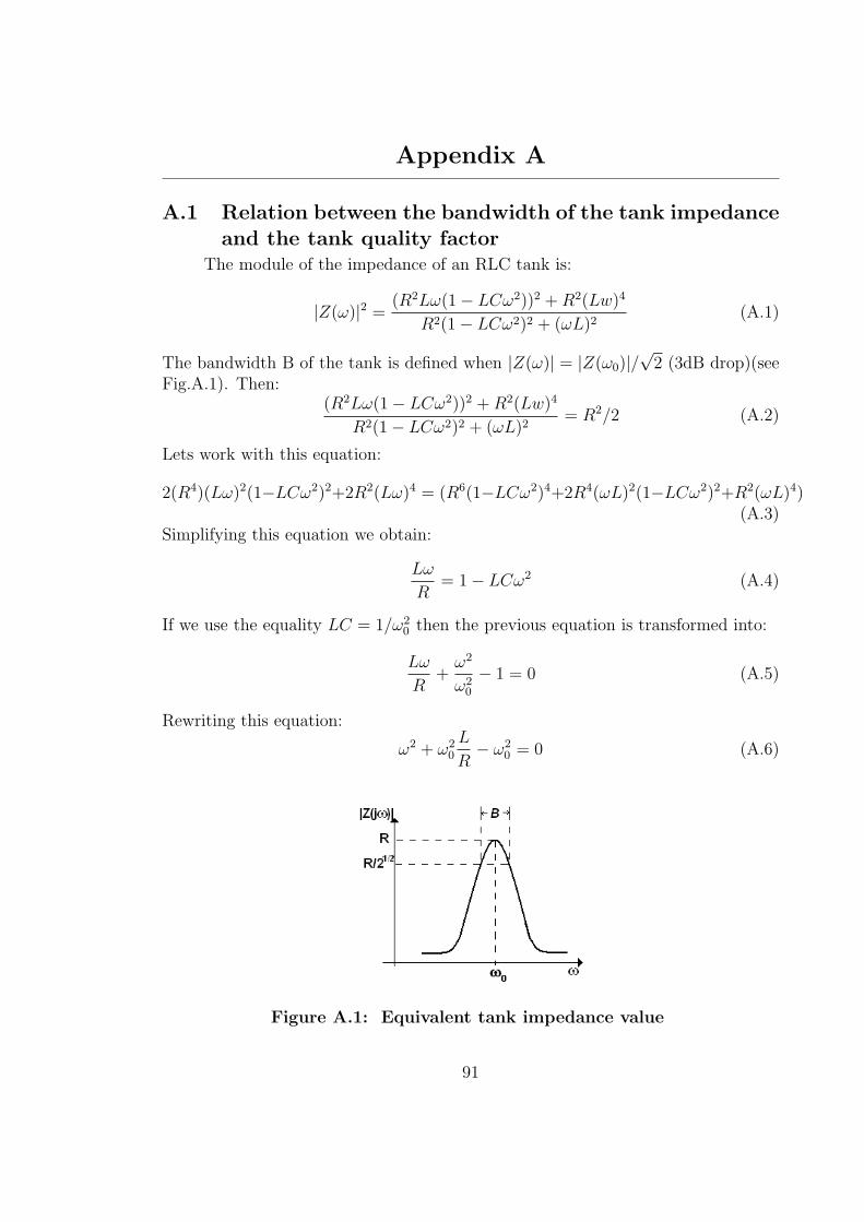
Appendix A
A.1 Relation between the bandwidth of the tank impedanceand the tank quality factor
The module of the impedance of an RLC tank is:
|Z(ω)|2 =(R2Lω(1− LCω2))2 +R2(Lw)4
R2(1− LCω2)2 + (ωL)2(A.1)
The bandwidth B of the tank is defined when |Z(ω)| = |Z(ω0)|/√
2 (3dB drop)(seeFig.A.1). Then:
(R2Lω(1− LCω2))2 +R2(Lw)4
R2(1− LCω2)2 + (ωL)2= R2/2 (A.2)
Lets work with this equation:
2(R4)(Lω)2(1−LCω2)2+2R2(Lω)4 = (R6(1−LCω2)4+2R4(ωL)2(1−LCω2)2+R2(ωL)4)(A.3)
Simplifying this equation we obtain:
Lω
R= 1− LCω2 (A.4)
If we use the equality LC = 1/ω20 then the previous equation is transformed into:
Lω
R+ω2
ω20
− 1 = 0 (A.5)
Rewriting this equation:
ω2 + ω20
L
R− ω2
0 = 0 (A.6)
Figure A.1: Equivalent tank impedance value
91
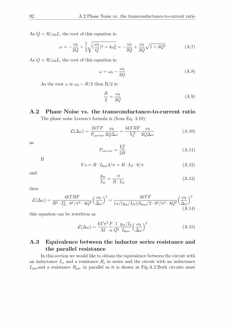
92 A.2 Phase Noise vs. the transconductance-to-current ratio
As Q = R/ω0L, the root of this equation is:
ω = − ω0
2Q+
1
2
√(ω0
Q)2 + 4ω2
0 = − ω0
2Q+ω0
2Q
√1 + 4Q2 (A.7)
As Q = R/ω0L, the root of this equation is:
ω = ω0 −ω0
2Q(A.8)
As the root ω is ω0 −B/2 then B/2 is:
B
2=ω0
2Q(A.9)
A.2 Phase Noise vs. the transconductance-to-current ratioThe phase noise Leeson’s formula is (from Eq. 3.10):
L(∆ω) =2kTF
Pcarrier
ω0
2Q∆ω=
4kTRF
V 20
ω0
2Q∆ω(A.10)
as
Pcarrier =V 2
0
2R(A.11)
IfV o = R · Ibias4/π = R · ID · 8/π (A.12)
andgm
ID=
α
R · ID(A.13)
then
L(∆ω) =4kTRF
R2 · I2D · 82/π2 · 4Q2
( ω0
∆ω
)2
=4kTF
(α/(gm/ID))Ibias/2 · 82/π2 · 4Q2
( ω0
∆ω
)2
(A.14)this equation can be rewritten as
L(∆ω) =kTπ2
32
F
α
1
Q2
gm/IdIbias
( ω0
∆ω
)2
(A.15)
A.3 Equivalence between the inductor series resistance andthe parallel resistance
In this section we would like to obtain the equivalence between the circuit withan inductance Ls and a resistance Rs in series and the circuit with an inductanceLparand a resistance Rpar in parallel as it is shown in Fig.A.2.Both circuits must

A. 93
Figure A.2: Equivalence of parallel circuit and series circuit
have an equivalent impedance, then
Zeq = Rs + jwLs = Rpar//jwLpar =RparjwLpar
Rpar + jwLpar
(A.16)
Then, separating the real and imaginary part of the equality
Rs + jwLs =Rparw
2L2par
R2par + w2L2
par
+ jwLparR
2par
R2par + w2L2
par
(A.17)
It means that
Rs =Rparw
2L2par
R2par + w2L2
par
(A.18)
Ls =LparR
2par
R2par + w2L2
par
(A.19)
As the denominator of EqsA.18 and A.19 are equal and, from Eq.4.5 Q = ωLS
RS
wLpar
Rpar
=Rs
wLs
=1
Q(A.20)
With Eqs.A.18 and A.20 we obtain the following formula:
Rpar + w2L2par −
w2L2par
Rs
Rpar = 0 (A.21)
Rpar
(1 +
1
Q2− Rpar
Q2Rs
)= 0 (A.22)
Rpar = (Q2 + 1)Rs =Q2 + 1
QwLs (A.23)
and with Eqs.A.19 and A.20 :
RparLs + w2L2parLs − LparR
2par = 0 (A.24)
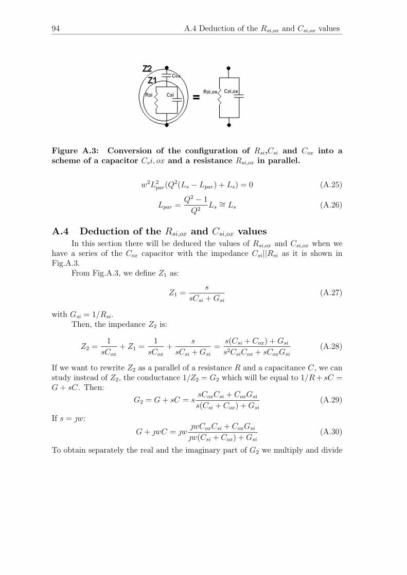
94 A.4 Deduction of the Rsi,ox and Csi,ox values
Figure A.3: Conversion of the configuration of Rsi,Csi and Cox into ascheme of a capacitor Csi, ox and a resistance Rsi,ox in parallel.
w2L2par(Q
2(Ls − Lpar) + Ls) = 0 (A.25)
Lpar =Q2 − 1
Q2Ls∼= Ls (A.26)
A.4 Deduction of the Rsi,ox and Csi,ox valuesIn this section there will be deduced the values of Rsi,ox and Csi,ox when we
have a series of the Cox capacitor with the impedance Csi||Rsi as it is shown inFig.A.3.
From Fig.A.3, we define Z1 as:
Z1 =s
sCsi +Gsi
(A.27)
with Gsi = 1/Rsi.Then, the impedance Z2 is:
Z2 =1
sCox
+ Z1 =1
sCox
+s
sCsi +Gsi
=s(Csi + Cox) +Gsi
s2CsiCox + sCoxGsi
(A.28)
If we want to rewrite Z2 as a parallel of a resistance R and a capacitance C, we canstudy instead of Z2, the conductance 1/Z2 = G2 which will be equal to 1/R+ sC =G+ sC. Then:
G2 = G+ sC = ssCoxCsi + CoxGsi
s(Csi + Cox) +Gsi
(A.29)
If s = w:
G+ wC = wwCoxCsi + CoxGsi
w(Csi + Cox) +Gsi
(A.30)
To obtain separately the real and the imaginary part of G2 we multiply and divide

A. 95
by the conjugate of the denominator:
G+ wC = w(wCoxCsi + CoxGsi)(w(Csi + Cox) +Gsi)
w2(Csi + Cox)2 +G2si
(A.31)
Working with this equation we obtain:
G+ wC = wCox(G
2si + w2(Csi + Cox)Csi)− wGsiC
2ox
w2(Csi + Cox)2 +G2si
(A.32)
Taking the real and the imaginary part:
G =w2GsiC
2ox
w2(Csi + Cox)2 +G2si
(A.33)
C =Cox(G
2si + w2(Csi + Cox)Csi)
w2(Csi + Cox)2 +G2si
(A.34)
We will call Rsi,ox = 1/G and Csi,ox = C as it is shown in Fig.A.3.As usually Csi is of the same order as Cox, C can be considered very similar to
Cox. Also as the denominator of G is bigger that the part that multiplies Gsi, thenG < Gsi.
To see which are the typical values of these variables, we will consider thevalues of Csi, Cox and Rsi of the technology used in this work. For 910MHz, Gsi '1/600Ω = 1.6e−3S, Csi ' 40fF and Cox = 160fF :
Rsi,ox =(2π910e6)2 · (200e−15)2 + (1.6e−3)2
(2π910e6)2 · 1.6e−3 · (160e−15)2Ω = 2.8kΩ (A.35)
C =160e−15((1.6e−3)2 + (2π910e6)2.(200e−15).(40e−15))
(2π910e6)2(200e−15)2 + (1.6e−3)2F = 117fF (A.36)
A.5 I-MOS varactor Gate capacitance versus iThe intrinsic capacitance of the varactor is (see 5.4):
Cgg = Cgs + Cgd + Cgb (A.37)
From [33] the expressions of Cgs and Cgd are:
Cgs =2
3Cox(
√1 + if − 1)
√1 + if + 2
√1 + ir
(√
1 + if +√
1 + ir)2(A.38)
Cgd =2
3Cox(
√1 + ir − 1)
√1 + ir + 2
√1 + if
(√
1 + if +√
1 + ir)2(A.39)
with if and ir the forward and reverse normalized currents defined in [26].
96 A.5 I-MOS varactor Gate capacitance versus i
As the drain source current ID = 0 and ID = IS(if − ir) then if = ir = i andCgs = Cgd.
Cgb is defined as:
Cgb = (1− 1
n)(Cox − Cgs − Cgd) =
n− 1
n(Cox − 2Cgs) (A.40)
And Cgs can be re-written in the following way:
Cgs =Cox
2
√1 + i− 1√
1 + i(A.41)
Then
Cgg = 2Cgs + (1− 1
n)(Cox − 2Cgs) =
n− 1
nCox +
2
nCgs (A.42)
Substituting the value of Cgs in the previous equation we obtain:
Cgg =n− 1
nCox +
2
n
(Cox
2
√1 + i− 1√
1 + i
)(A.43)
Rearranging the equation we finally obtain:
Cgg =Cox
n(n− 1√
1 + i) (A.44)
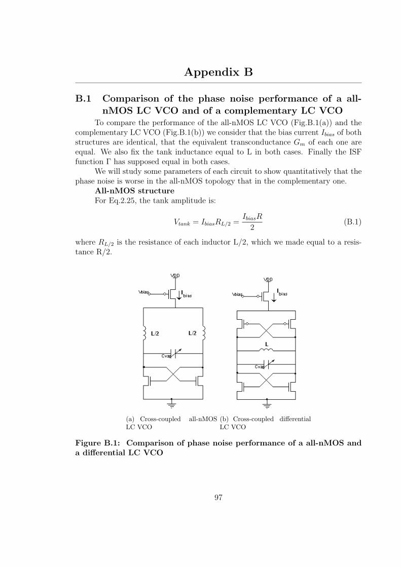
Appendix B
B.1 Comparison of the phase noise performance of a all-nMOS LC VCO and of a complementary LC VCO
To compare the performance of the all-nMOS LC VCO (Fig.B.1(a)) and thecomplementary LC VCO (Fig.B.1(b)) we consider that the bias current Ibias of bothstructures are identical, that the equivalent transconductance Gm of each one areequal. We also fix the tank inductance equal to L in both cases. Finally the ISFfunction Γ has supposed equal in both cases.
We will study some parameters of each circuit to show quantitatively that thephase noise is worse in the all-nMOS topology that in the complementary one.
All-nMOS structureFor Eq.2.25, the tank amplitude is:
Vtank = IbiasRL/2 =IbiasR
2(B.1)
where RL/2 is the resistance of each inductor L/2, which we made equal to a resis-tance R/2.
(a) Cross-coupled all-nMOSLC VCO
(b) Cross-coupled differentialLC VCO
Figure B.1: Comparison of phase noise performance of a all-nMOS anda differential LC VCO
97

98B.1 Comparison of the phase noise performance of a all-nMOS LC VCO and of a
complementary LC VCO
As qmax (see Eq.3.12) is proportional to the tank voltage:
qmax ∝IbiasR
2(B.2)
If Gm is the total transconductance, the transconductance of each nMOS tran-sistor is gm = 2Gm.
Also in this structure the total differential white noise power due to the tran-sistors is (see Eq.3.24):
i2tot =i2n2
= 2kTγ(2Gm) = 4kTγGm (B.3)
with k the Boltzmann constant, T the absolute temperature.Re-writing the Eq.3.19 of Chap.3:
L(∆ω) = 10 · log( i2n
∆fΓ2
rms
2q2max∆ω
2
)(B.4)
the phase noise is
LallnMOS ∝i2nq2max
= (4kTγGm)(R2/4) = 16kTγGmR2 = L (B.5)
Complementary structureIn this case the tank amplitude is:
Vtank = IbiasRL = IbiasR (B.6)
Here the resistance is the double than in the all-nMOS case.qmax is:
qmax ∝ IbiasR (B.7)
Total differential white noise power due to the four transistors is:
i2tot =i2n + i2p
2= 4kTγGm (B.8)
Then the phase noise is
Lcomp ∝i2n + i2pq2max
=4kTγGm
R2= 4L (B.9)
Therefore the complementary structure has approximately four times lessphase noise that the all-nMOS one. What makes the difference is the higher va-lue of qmax in the complementary structure than in the all-nMOS one (see [72]).
This discussion can be seen from another point of view: instead of comparing
B. 99
both circuits with an equal bias current, we can vary the current until both circuitshave the same phase noise. It can be seen that the current of the all-nMOS structurehas to be two times higher than the complementary structure.

100
Appendix C
C.1 Layout of the PCBA PCB has been fabricated to test the designed VCO, among other circuits.
The top and bottom layers are depicted in Figs.C.1(a) and C.1(b). We have useddecoupling ceramic capacitors of 100pF and 100nF between ground (GND) and allthe supply pads (VDD). We use a ground plane to minimize the path of the signal.At the point of the external supply connection we also put a tantalum capacitor of10mF. To fix as much as possible the various ”virtual ground” of the circuit (thesources of the two cross-coupled transistor blocks and the bias varactor point) weput capacitors of 100pF between them and ground.
The fabricated PCB is shown in Figs.C.2(a) and C.2(b) (top and down layers).
101
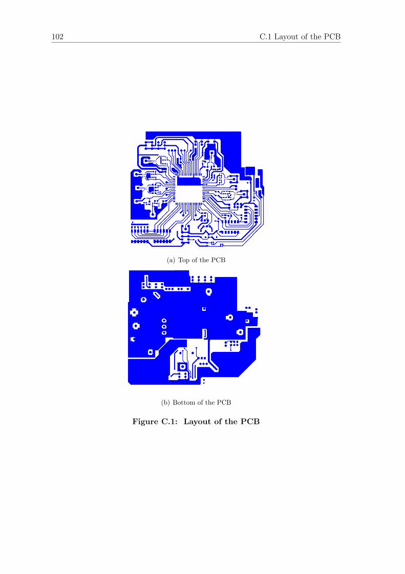
102 C.1 Layout of the PCB
(a) Top of the PCB
(b) Bottom of the PCB
Figure C.1: Layout of the PCB
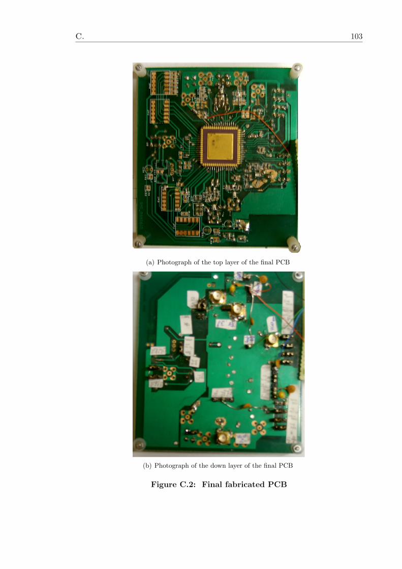
C. 103
(a) Photograph of the top layer of the final PCB
(b) Photograph of the down layer of the final PCB
Figure C.2: Final fabricated PCB
Bibliography
[1] S. Mohan, M. del Mar Hershenson, S. Boyd, and T. Lee, “Simple accurate ex-pressions for planar spiral inductances,” IEEE Journal of Solid-State Circuits,vol. 34, no. 10, pp. 1419–1424, Oct. 1999.
[2] A. A. Abidi, “RF CMOS comes of age,” IEEE Journal of Solid-State Circuits,vol. 39, no. 4, pp. 549–561, Apr. 2004.
[3] E. Hegazi and A. A. Abidi, “A 17-mW transmitter and frequency synthesizer for900-MHz gsm fully integrated in 0.35-µm CMOS,” IEEE Journal of Solid-StateCircuits, vol. 38, no. 5, pp. 782–792, May 2003.
[4] P. Quinlan, P. Crowley, M. Chanca, S. Hudson, B. Hunt, K. Mulvaney, G. Retz,C. E. OSullivan, and P. Walsh, “A multimode 0.3200-kb/s transceiver for the433/868/915-MHz bands in 0.25-µm CMOS,” IEEE Journal of Solid-State Cir-cuits, vol. 39, no. 12, pp. 2297–2310, Dec. 2004.
[5] E. Duvivier, G. Puccio, S. Cipriani, L. Carpineto, P. Cusinato, B. Bisanti,F. Galan, F. Chalet, F. Coppola, S. Cercelaru, N. Vallespin, J.-C. Jiguet, andG. Sirna, “A fully integrated zero-IF transceiver for GSM-GPRS quad-bandapplication,” IEEE Journal of Solid-State Circuits, vol. 39, no. 6, pp. 952–955,June 2004.
[6] J. A. Weldon, R. S. Narayanaswami, J. C. Rudell, L. Lin, M. Otsuka, S. Dedieu,L. Tee, K.-C. Tsai, C.-W. Lee, and P. R. Gray, “A 1.75-GHz highly integra-ted narrow-band CMOS transmitter with harmonic-rejection mixers,” IEEEJournal of Solid-State Circuits, vol. 36, no. 12, pp. 2003 – 2015, Dec. 2001.
[7] Y. Wu and V. Aparin, “A monolithic low phase noise 1.7ghz CMOS VCOfor zero-IF cellular CDMA receivers,” IEEE International Solid-State CircuitsConference, vol. XVII, pp. 396 – 397, Feb. 2004.
[8] C. Guo, C.-W. Lo, Y.-W. Choi, I. Hsu, T. Kan, D. Leung, A. Chan, and H. C.Luong, “A fully integrated 900-MHz CMOS wireless receiver with on-chip RFand IF filters and 79-dB image rejection,” IEEE Journal of Solid-State Circuits,vol. 37, no. 8, pp. 1084–1089, Aug. 2002.
[9] H. Darabi, S. Khorram, H.-M. Chien, M.-A. Pan, S. Wu, S. Moloudi, J. C.Leete, J. J. Rael, M. Syed, R. Lee, B. Ibrahim, M. Rofougaran, and A. Rofou-garan, “A 2.4-GHz CMOS transceiver for Bluetooth,” IEEE Journal of Solid-State Circuits, vol. 36, no. 12, pp. 2016 – 2024, Dec. 2001.
[10] T. Lee, “CMOS RF:(still) no longer an oximoron,” IEEE Radio FrequencyIntegrated Circuits Symposium, pp. 3–6, 1999.
104

BIBLIOGRAPHY 105
[11] “802.15.4,” IEEE, The Institute of Electrical and Electronics Engineers, Inc.3 Park Avenue, New York, NY 10016-5997, USA, (http://standards.ieee.org/,Standard, Oct. 2003.
[12] A.-S. Porret, T. Melly, D. Python, C. C. Enz, and E. A. Vittoz, “An ultralow-power UHF transceiver integrated in a standard digital CMOS process: Ar-quitecture and receiver,” IEEE Journal of Solid-State Circuits, vol. 36, no. 3,pp. 452–464, Mar. 2001.
[13] P. Andreani and S. Mattisson, “A 2.4GHz monolithic VCO based on an MOSvaractor,” Proccedings ISCAS’99, vol. II, pp. 557–560, May-June 1999.
[14] J. Maget, M. Tiebout, and R. Kraus, “Influence of novel MOS varactors on theperformance of a fully integrated UMTS VCO in standard 0.25 − µm CMOStechnology,” IEEE Journal of Solid-State Circuits, vol. 37, no. 7, pp. 953–958,July 2002.
[15] J. Craninckx and M. S. J. Steyaert, “A 1.8 GHz low-phase-noise CMOS VCOusing optimized hollow spiral inductors,” IEEE Journal of Solid-State Circuits,vol. 32, no. 5, pp. 736–744, May 1997.
[16] T. H. Teo, Y. Choi, H. Liao, Y.-S. Xiong, and J. S. Fu, “Characterizationof symmetrical spiral inductor in 0.35µm cmos technology for RF appliction,”Solid-State Electronics, vol. 48, pp. 1643–1650, Apr. 2004.
[17] A. Jerng and C. G. Soldini, “The impact of device type and sizing of phasenoise mechanisms,” IEEE Journal of Solid-State Circuits, vol. 40, no. 2, pp.360–369, Feb. 2005.
[18] B. D. Muer, M. Borremans, M. Steyaert, and G. L. Puma, “A 2-GHz low-phase-noise integrated LC-VCO set with flicker-noise upconvertion minimization,”IEEE Journal of Solid-State Circuits, vol. 7, no. 35, pp. 1034–1038, July 2000.
[19] F. Svelto, S. Deantoni, and R. Castello, “A 1.3ghz low-phase noise fully tunabloCMOS LC VCO,” IEEE Journal of Solid-State Circuits, vol. 35, no. 3, pp. 356–361, Mar. 2000.
[20] D. Ham and A. Hajimiri, “Concepts and methods in optimization of integratedLC VCOs,” IEEE Journal of Solid-State Circuits, vol. 36, no. 6, pp. 896–909,June 2001.
[21] A. Hajimiri and T. H. Lee, “Design issues in CMOS differential LC oscillators,”IEEE Journal of Solid-State Circuits, vol. 34, no. 5, pp. 717–724, May 1999.
[22] J. Burghartz, D. Eldestein, M. Soyuer, H. Ainspan, and K. Jenkins, “RF cir-cuit design aspects of spiral inductors on silicon,” IEEE Journal of Solid-StateCircuits, vol. 33, no. 12, pp. 2028–2034, Dec. 1998.
106 BIBLIOGRAPHY
[23] N. Nguyen and R. Meyer, “Si IC-compatible inductors and LC passive filters,”IEEE Journal of Solid-State Circuits, vol. 25, no. 4, pp. 1028–1031, 1990.
[24] A. M. Niknejad and R. G. Meyer, “Analysis, design, and optimization of spi-ral inductors and transformers for Si RF ICs,” IEEE Journal of Solid-StateCircuits, vol. 33, no. 10, pp. 1470–1481, Oct. 1998.
[25] F. Silveira, D. Flandre, and P. G. A. Jespers, “A gm/id based methodologyfor the design of CMOS analog circuis and its applications to the synthesis ofa silicon-on-insulator micropower OTA,” IEEE Journal of Solid-State Circuits,vol. 31, no. 9, pp. 1314–1319, Sept. 1996.
[26] A. I. A. Cuhna, M. C. Schneider, and C. Galup-Montoro, “An MOS transistormodel for analog circuit design,” IEEE Journal of Solid-State Circuits, vol. 33,no. 10, pp. 1510–1519, Oct. 1998.
[27] C.-M. Hung and K. K. O, “A packaged 1.1-GHz CMOS VCO with phase noiseof -126 dBc/Hz at a 600-kHz offset,” IEEE Journal of Solid-State Circuits,vol. 35, no. 1, pp. 100–103, Jan. 2000.
[28] S. Tadjpour, E. Cijvat, E. Hegazi, and A. A. Abidi, “A 900-MHz dual-conversion low-IF GSM receiver in 0.35µm CMOS,” IEEE Journal of Solid-State Circuits, vol. 36, no. 12, pp. 1992–2002, Dec. 2001.
[29] D. Leenaerts, J. van der Tang, and C. Vaucher, Circuit Design for RF Transcei-vers. Dordrecht, The Netherlands: Kluwer Academic Publishers, 2001, iSBN0-7923-7551-3.
[30] N. M. Nguyen and R. G. Meyer, “Start-up and frequency stability in high-frequency oscillators,” IEEE Journal of Solid-State Circuits, vol. 27, no. 5, pp.810–820, May 1992.
[31] R. L. Bunch, “A fully monolothic 2.5GHz LC voltage controlled oscillator in0.35µm CMOS technology,” Master Thesis, Virginia Polytechnic Institute andState University, Blacksburg,Virginia, Apr. 2001.
[32] T. Lee and A. Hajimiri, “Oscillator phase noise: a tutorial,” IEEE Journal ofSolid-State Circuits, vol. 35, no. 3, pp. 326–336, Mar. 2000.
[33] C. Galup-Montoro, M. C. Schneider, and A. I. A. Cuhna, Low-Voltage/Low-Power Integrated Circuits and Systems, ieee press ed. E.Sanchez-Sinencio andA. Andreou, 1999, ch. A Current-based MOSFET Model for Integrated CircuitDesign, pp. 7–55.
[34] T. Manku, “Microwave CMOS- device physics and design,” IEEE Journal ofSolid-State Circuits, vol. 34, no. 3, pp. 277–285, Mar. 1999.
BIBLIOGRAPHY 107
[35] Y.P.Tsividis, Operation and Modelling of the MOS Transistor, 2nd ed. OxfordUniversity Press, 2000.
[36] C. Enz, F.Krummenacher, and E. Vittoz, “An analytical MOS transistor modelvalid in all regions of operation and dedicated to low-voltage and low-currentapplications,” Analog Integrated Circuits and Signal Processing, vol. 8, pp. 83–114, 1995.
[37] C. Vaucher, Architectures for RF Frequency Synthesizers, ser. Analog Circuitand Signal Processing. Dordrecht: Kluwer Academic Publishers, 2002, iSBN:1-4020-7120-5.
[38] A. J.Rael, “Physical processes of phase noise in differential lc oscillators,” IEEE2000 Custom integrated circuit conference, pp. 569–571, 2000.
[39] A. Hajimiri, Trade Offs in Analog Cirtuit Design: the Designer’s Companion.Printed in Netherlands: Kluwer Academic Publishers, 2002, ch. Trade offs inOscillator Phase Noise, pp. 551–589, tomazou et al. (eds).
[40] H. W.Johnson and M. Graham, High-Speed Digital Design: a Handbook of BlackMagic. New Jersey: Prentice Hall, 1993.
[41] J. Gerrits(CSEM) and D. G. Microelectronics), “RF CMOS IC design guideli-nes,” CSEM,” Design Guidelines, Feb. 2001.
[42] A. Arnaud and C. Galup-Montoro, “A compact model for flicker noise in MOStransistors for analog circuit design,” IEEE Transactions on Electron Devices,vol. 50, no. 8, pp. 1815–1818, Aug. 2003.
[43] “Matlab,” software program, 2005, www.mathworks.com.
[44] A. Pun, T. Yeung, J. Lau, F. Clement, and D. Su, “Substrate noise couplingthough planar spiral inductor,” IEEE Journal of Solid-State Circuits, vol. 33,no. 6, pp. 877–884, June 1998.
[45] T. Blalack, Y. Lecklercq, and P. Yue, “On-chip RF isolation techniques,”http : //www.techonine.com/community/edresource/featurearticle/21590,Jan. 2003, searched:25/03/05.
[46] A. Hajimiri, “A general theory of phase noise in electrical oscillators,” IEEEJournal of Solid-State Circuits, vol. 33, no. 2, pp. 179–194, Feb. 1998.
[47] D. Leeson, “A simple model of feedback oscillator noise spectrum,” Proceedingsof the IEEE, vol. 54, pp. 329–330, Feb. 1966.
[48] L. Dai and R. Harjani, Design of High-Performance CMOS Voltage ControlledOscillators, ser. analog circuit and signal processing. Boston: Kluwer academicpublishers, 2003, iSBN: 1-4020-7238-4.
108 BIBLIOGRAPHY
[49] A.A.Abidi, “High frequency noise measuremens on FET’s with small dimen-sions,” IEEE Transactions on Electron Devices, vol. ED-33, no. 11, pp. 1801–1805, Nov. 1986.
[50] A. Hajimiri and T. Lee, “Phase noise in differential LC oscillators,” Symposiumon VLSl Circuits Digest of Technical Papers, no. 5.1, pp. 48–51, 1998.
[51] A. Arnaud and C. G. Montoro, “Consistent noise models for analysis and de-sign of cmos circuits,” IEEE Transactions on Circuits and Systems—Part I:Fundamental Theory and Applications, vol. 51, no. 10, pp. 1909–1915, Oct.2004.
[52] P. Kinget, Analog Circuit Design. Kluwer, 1999, ch. Integrated GHz VoltageControlled Oscillators, pp. 353–381.
[53] A. M. Niknejad, “Analyis of Si inductors and transformers for IC’s(ASITIC),”2000, http://rfic.eecs.berkeley.edu/ niknejad/asitic.html.
[54] J. R.Long and M. A. Copeland, “The modeling, characterization and design ofmonolithic inductors for silicon RF IC’s,” IEEE Journal of Solid-State Circuits,vol. 32, no. 3, pp. 357–369, Mar. 1997.
[55] Y. K. Koutsoyannopoulos and Y. Papananos, “Systematic analysis and mode-ling of integrated inductors and transformers in RF IC design,” IEEE Transac-tions on Circuits and Systems—Part II: Analog and Digital Signal Processing,vol. 47, no. 8, pp. 699–713, Aug. 2000.
[56] P. Yue and S. Wong, “Design strategy on on-chip inductors for highly integratedRF systems,” DAC, 1999.
[57] P. Yue, C. Ryu, JackLau, T. Lee, and S. Wong, “A physical model for pla-nar spiral inductors on silicon,” 1996 International Electron Devices MeetingTechnical Digest, pp. 155–158, Dec. 1996.
[58] P. Yue and S. Wong, “Physical modelling of spiral inductor on silicon,” IEEETransactions on Electron Devices, vol. 47, no. 3, pp. 560–568, Mar. 2000.
[59] H. M. Greenhouse, “Design of planar rectangular microelectronic inductors,”IEEE Transactions on Parts, Hybrids and Packaging, vol. 10, no. 2, pp. 101–109, June 1974.
[60] H. A. Wheeler, “Simple inductance formulas for radio coils,” Proceedings IRE,vol. 16, no. 10, pp. 1398–1400, Oct. 1928.
[61] “Cadence,” 2005, www.cadence.com.
[62] C. P. Group and MIT, “Fasthenry,” http://rleweb.mit.edu/vlsi/codes.htm.

BIBLIOGRAPHY 109
[63] F.Svelto, S.Manzini, and R. Castello, “A three terminal varactor for RF IC’s inStandard CMOS technologies,” IEEE Transactions on Electron Devices, vol. 47,no. 4, pp. 893–895, Apr. 2000.
[64] A. Kiranas and Y. Papanaos, “Design issues towards the integration of passivecomponents in silicon RF VCOs,” -, vol. -, no. -, pp. 311–314, - 1998.
[65] P. Andreani and S. Mattison, “On the use of MOS varactors in RF VCO’s,”IEEE Journal of Solid-State Circuits, vol. 35, no. 6, pp. 905–910, June 2000.
[66] R. L. Bunch and S. Raman, “Large-signal analysis of MOS Varactors in CMOS-Gm LC VCOs,” IEEE Journal of Solid-State Circuits, vol. 38, no. 8, pp. 1325–1332, Aug. 2003.
[67] D. Integrated, “Smash 5.2.2,” http : //www.dolphin −integration.com/medal/smash/smashoverview.html, 2004.
[68] S.-M. Yim, T. Chen, and K. K.O, “The effect of a ground shield on the cha-racteristics and performance of spiral inductors,” IEEE Journal of Solid-StateCircuits, vol. 37, no. 2, pp. 237–244, Feb. 2002.
[69] L. Barboni, R.Fiorelli, and F.Silveira, “Low power rf design blocks in weak andmoderate inversion,” XI Iberchip Workshop, Baha, Brasl, Mar 2005.
[70] ——, “Design and power optimization of cmos rf blocks operating in the mode-rate inversion region,” Proceedings of the 18th annual Symposium on IntegratedCircuits and System Design, SBCCI, Florianolis, Brazil, vol. I, pp. 15–20, Sept2005.
[71] ——, “A tool for design exploration and power optimization of cmos rf circuitblocks,” May 2006, work presented for evaluation for ISCAS 2006.
[72] R. Aparicio and A. Hajimiri, “A noise-shifting differential colpitts VCO,” IEEEJournal of Solid-State Circuits, vol. 37, no. 12, pp. 1728–1736, Dec. 2002.


![RF Module Design - [Chapter 7] Voltage-Controlled Oscillator](https://img.pdfslide.net/doc/110x75/55cebbaebb61eb912f8b45f9/rf-module-design-chapter-7-voltage-controlled-oscillator.jpg)


