Embed Size (px)
Citation preview
Features ■ Low Offset Voltage: 50µV Maximum ■ Low Drift: 0.5µV/ºC Maximum ■ Low Input Bias Current: 3nA maximum ■ Wide Supply Range: ±2.25V ~ ±18V ■ Low Quiescent Current: 1.4mA ■ Input Over-Voltage Protection ■ Available as SOP8, DIP8 package
Applications ■ Medical Instrumentation ■ Data Acquisition ■ RTD Sensor Amplifier ■ Bridge Amplifier ■ Thermocouple Amplifier
General Description HG620 is a low-power, general purpose instrumentation amplifiers offering excellent accuracy. The versatile 3-op amp design and small size make these amplifiers ideal for a wide range of applications. A single external resistor sets any gain from 1 to 10,000. The HG620 gain equation is compatible with the AD620. The HG620 is laser-trimmed for very low offset voltage (50µV), drift (0.5µV/ºC) and high common mode rejection. The HG620 operates with power supplies as low as ±2.25, and quiescent current is only 1.4mA, ideal for battery-operated systems. The HG620 is available in 8-pin plastic DIP8 and SOP8 packages, specified for the -40 ºC to +85 ºC temperature range.
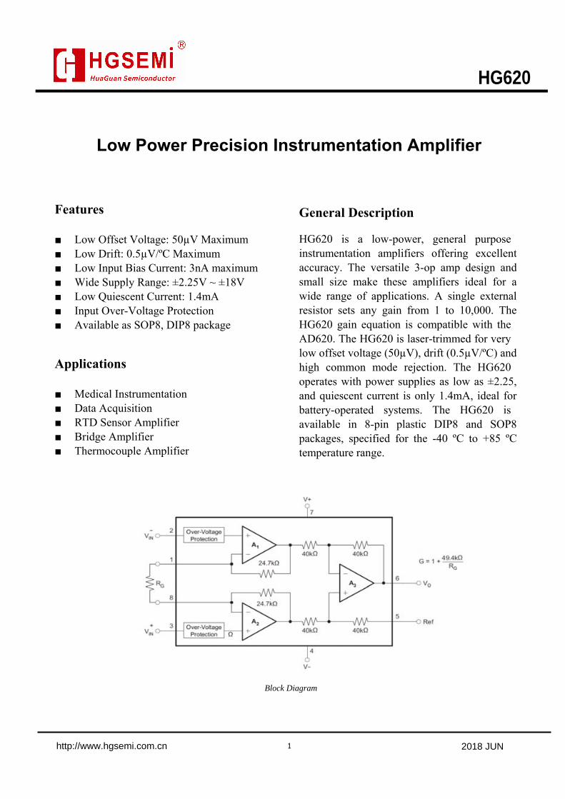
Block Diagram
Low Power Precision Instrumentation Amplifier
1
http://www.hgsemi.com.cn 2018 JUN
HG620
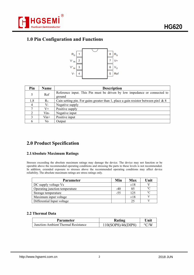
1.0 Pin Configuration and Functions
Pin Name Description
5 Ref Reference input. This Pin must be driven by low impedance or connected to ground
1,8 RG Cain setting pin. For gains greater than 1, place a gain resistor between pin1 & 8 4 V- Negative supply 7 V+ Positive supply 2 Vin- Negative input 3 Vin+ Positive input 6 Vo Output
2.0 Product Specification 2.1Absolute Maximum Ratings Stresses exceeding the absolute maximum ratings may damage the device. The device may not function or be operable above the recommended operating conditions and stressing the parts to these levels is not recommended. In addition, extended exposure to stresses above the recommended operating conditions may affect device reliability. The absolute maximum ratings are stress ratings only.
Parameter Min Max Unit DC supply voltage Vs ±18 V Operating junction temperature -40 85 °C
Storage temperature -55 125 °C
Maximum input voltage ±18 V
Differential Input voltage 25 V
2.2 Thermal Data
Parameter Rating Unit Junction-Ambient Thermal Resistance 110(SOP8)/46(DIP8) °C/W
2
http://www.hgsemi.com.cn 2018 JUN
HG620
2.3 Recommended Operating Conditions
Parameter Rating Unit DC Supply Voltage ±2.25V ~ ±18V V Input common-mode voltage range (V-)+2 ~ (V+)-2 V
Operating ambient temperature -40 to +85 °C
2.4 Electrical Characteristics (Typical values are tested at TA=25 oC, Vs=±15V)
Parameter Symbol Conditions Min. Typ. Max. Unit
Input Offset Voltage VIO - ±15 ±50 µV
Input Offset Voltage Drift TC 0.1 0.6 µV/ºC
Input Offset Current IIO - ±1 ±5 nA
Input Bias Current IBIAS - ±2 ±5 nA
Operating Current ICC - 1.4 1.8 mA
Common Mode Input Voltage Range VICM ±13 ±14 - V
Common Mode Rejection Range CMRR Rs≤10kΩ 70 100 - dB
Supply Voltage Rejection Ratio SVRR Rs≤10kΩ 80 100 - dB
Output Voltage Swing VO(P-P) RL ≥10kΩ ±13 ±13.8 - V
Short Circuit Current ISC - ±28 - mA
Gain Bandwidth Product GBW CL =100pF, RL = 10kΩ - 1000 - kHz
Slew Rate SR CL =100pF, RL=10kΩ, Av=1 - 1.2 - V/µs
Input Noise Voltage eN f= 1kHz
- 6.0 - nV/ √Hz
3.0 Functional Description 3.1 Overview The HG620 instrumentation amplifier is a type of differential amplifier that has been outfitted
with input protection circuit and input buffer amplifiers, which eliminate the need for input
impedance matching and make the amplifier particularly suitable for use in measurement and test
equipment. Additional characteristics of the HG620 include a v ery low DC offset, low drift, low
noise, very high open-loop gain, very high common-mode rejection ratio, and very high input
impedances.
3
http://www.hgsemi.com.cn 2018 JUN
HG620
4
http://www.hgsemi.com.cn 2018 JUN
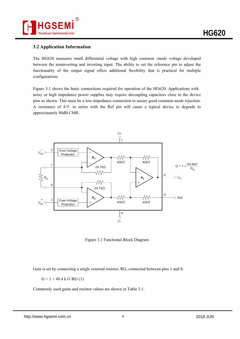
HG620 3.2 Application Information The HG620 measures small differential voltage with high common -mode voltage developed
between the noninverting and inverting input. The ability to set the reference pin to adjust the
functionality of the output signal offers additional flexibility that is practical for multiple
configurations.
Figure 3.1 shows the basic connections required for operation of the HG620. Applications with
noisy or high impedance power supplies may require decoupling capacitors close to the device
pins as shown. This must be a low-impedance connection to assure good common-mode rejection.
A resistance of 8Ω in series with the Ref pin will cause a typical device to degrade to
approximately 80dB CMR.
Figure 3.1 Functional Block Diagram Gain is set by connecting a single external resistor, RG, connected between pins 1 and 8:
G = 1 + 49.4 kΩ/RG (1)
Commonly used gains and resistor values are shown in Table 3.1.
Important statement:
Huaguan Semiconductor Co,Ltd. reserves the right to changethe products and services provided without notice. Customersshould obtain the latest relevant information before ordering,and verify the timeliness and accuracy of this information.
Customers are responsible for complying with safetystandards and taking safety measures when using ourproducts for system design and machine manufacturing toavoid potential risks that may result in personal injury orproperty damage.
Our products are not licensed for applications in life support,military, aerospace, etc., so we do not bear the consequencesof the application of these products in these fields.
Our documentation is only permitted to be copied withoutany tampering with the content, so we do not accept anyresponsibility or liability for the altered documents.
5
http://www.hgsemi.com.cn 2018 JUN
HG620