Embed Size (px)
Citation preview
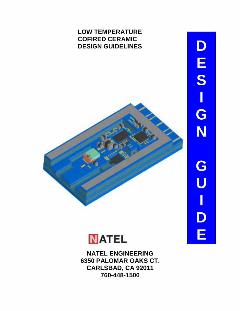
LOW TEMPERATURE COFIRED CERAMIC DESIGN GUIDELINES
NATEL ENGINEERING 6350 PALOMAR OAKS CT.
CARLSBAD, CA 92011 760-448-1500
D E S I G N
G U I D E

LTCC DESIGN GUIDELINES
DATE: 8/16/2011 REV: A PAGE NO: 2 NATEL ENGINEERING, INC – 6350 PALOMAR OAKS CT. – CARLSBAD, CA 92011 – 760-448-1500
UNPUBLISHED WORK – ALL RIGHTS RESERVED This design guide is for the use of Natel Engineering customers and may not be reproduced
without the express permission of Natel Engineering Inc.
TABLE OF CONTENTS
PAGE
Capabilities 3-5
Overview 6
STANDARD DESIGN CONSIDERATIONS
Conductors 7 Conductor Line width and spacing 7 Conductor to edge of substrate clearance 8 Ground and power planes 9 Vias 10 Electrical Vias 10 Catch Pads 11 Electrical via to via spacing on the same layer 12 Electrical via stagger 13 Electrical via to edge of substrate 14 RF vias 14 Thermal vias 15-16 Cavities 17 Cavity bottom conductor to cavity wall clearance 17 Exposed/buried conductor to cavity wall clearance 17 Via to cavity wall clearance 18 Bond shelf 18 Cavity to cavity spacing 19 Special high frequency design provisions 20 Resistors 21 Resistor sheet values 21 Minimum resistor tolerance 22 Resistor to conductor termination overlap 23 Minimum resistor length 24

LTCC DESIGN GUIDELINES
DATE: 8/16/2011 REV: A PAGE NO: 3 NATEL ENGINEERING, INC – 6350 PALOMAR OAKS CT. – CARLSBAD, CA 92011 – 760-448-1500
TABLE OF CONTENTS PAGE
Resistor to resistor spacing 25 Resistor to edge of substrate clearance 26 Resistor over coat overlap 27 Capacitors 28-29 Inductors 30 Post Fired Conductors 31 Cover pad design considerations 31 Metal distribution 32 Soldering 33 Soldering design considerations 33 Solder alloys 34 Material thermal properties 35 Electrical and mechanical properties of LTCC Table of Material thermal properties 35 Table of electrical and mechanical properties of LTCC 36 Microwave insertion loss of Ferro A6 and Dupont 951 to 40 GHz 37 Data base and documentation conventions 38-40
Appendix Sample ring frame drawing A Sample Critical dimensions table B
Those wishing to obtain an electronic version of this design guide may do so from Natel Engineering’s internet Home Page. Our address is http://www.natelengr.com.

LTCC DESIGN GUIDELINES
DATE: 8/16/2011 REV: A PAGE NO: 4 NATEL ENGINEERING, INC – 6350 PALOMAR OAKS CT. – CARLSBAD, CA 92011 – 760-448-1500
NATEL ENGINEERING CAPABILITIES
MATERIAL SYSTEMS
• DUPONT 951 TAPE SYSTEM ALL GOLD MIXED SILVER/GOLD SYSTEM PT/AU – PD/AG – GOLD – COPPER – SILVER – SURFACE METALIZATIONS ALL SILVER
• FERRO A6 TAPE SYSTEM MIXED SILVER/GOLD SYSTEM ALL GOLD PT/AU – PD/AG – GOLD – COPPER – SILVER – SURFACE METALIZATIONS ALL SILVER
• HERAEUS TAPE SYSTEM (Available from C-MAC GMBH; Villingen Germany) Zero Shrink Process MIXED SILVER/GOLD SYSTEM ALL GOLD PT/AU – PD/AG – GOLD – COPPER – SILVER – SURFACE METALIZATIONS ALL SILVER
• EMCA TAPE SYSTEM MIXED SILVER/GOLD SYSTEM ALL GOLD PT/AU – PD/AG – GOLD – COPPER – SILVER – SURFACE METALIZATIONS ALL SILVER

LTCC DESIGN GUIDELINES
DATE: 8/16/2011 REV: A PAGE NO: 5 NATEL ENGINEERING, INC – 6350 PALOMAR OAKS CT. – CARLSBAD, CA 92011 – 760-448-1500
NATEL ENGINEERING CAPABILITIES
SOLDER/EPOXY ATTACHMENT – RING FRAMES HEAT SINKS LEADS AND TIE BARS LOW/HIGH TEMPERATURE SOLDER ALLOYS
CU – MO – CU, CU-W, KOVAR / NI-FE SEAL RING, PINS AND LEADS
COPPER LEADS AND PINS
CERAMIC TIE BAR ATTACHMENT
SYSTEM TECHNOLOGY LTCC DIGITAL/ANALOG/MICROWAVE SUBSTRATES
INTEGRAL MCM AND RF PACKAGING
BALL GRIND ARRAYS
PIN GRIND ARRAYS
INTEGRATED PASSIVE COMPONETS – RESISTORS, CAPACITORS, INDUCTORS AND FILTERS
SERVICES LTCC
THICK FILM
CERAMIC MATCHING
MCM DESIGN AND DATA CONVERSION
SOLDER
LTCC DESIGN GUIDELINES
DATE: 8/16/2011 REV: A PAGE NO: 6 NATEL ENGINEERING, INC – 6350 PALOMAR OAKS CT. – CARLSBAD, CA 92011 – 760-448-1500
OVERVIEW This document summarizes the design guides for use with Low Temperature Co-fired Ceramics (LTCC). These design guides define three levels of producibility as follows:
PROOF OF CONCEPT / DESIGN (POC / POD)
Substrates designed to POC / POD levels of producibility are fabricated in an environment that pushes current state of the art LTCC process. Normal tolerances on this product are exceeded resulting in a higher risk situation where excessive touch up, rework and lower yields may have an impact on producibility scheduling and cost.
LOW VOLUME Substrates designed to these guidelines are capable of being produced with minimum inspection, touchup and rework resulting in reduced cost while maintaining acceptable circuit performance.
PRODUCTION Products designed to these guidelines are fabricated in a semi-automated and manual production environment. These layout guides encourage larger geometries and wider tolderances to reduce inspection and eliminate rework. The overall goal is to produce product at the lowest possible price while maintaining aggressive shipment schedules.
Minimum and preferred dimensions
Minimum and preferred dimensions have been provided whenever possible. If preferred dimensions are provided they should be considered the optimum for the process. When a preferred condition is not provided, the condition defined should be considered a minimum. Good design practice calls for use of minimums only in circumstances where performance and fit cannot tolerate more liberal preferred limits. Use of minimums should be avoided whenever possible.
Physical Considerations
The minimum number of tape layers for any LTCC substrate is three (.015”). Any design using a LTCC substrate should allow a ± .5% shrinkage variable.
The following documentation provides a detailed description of allowable shapes, dimensions and spacings for designing LTCC substrates and packages.
LTCC DESIGN GUIDELINES
DATE: 8/16/2011 REV: A PAGE NO: 7 NATEL ENGINEERING, INC – 6350 PALOMAR OAKS CT. – CARLSBAD, CA 92011 – 760-448-1500
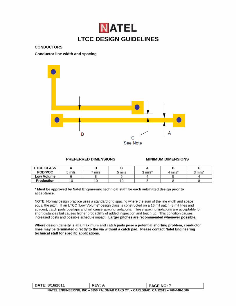
CONDUCTORS
Conductor line width and spacing
PREFERRED DIMENSIONS MINIMUM DIMENSIONS
LTCC CLASS A B C A B C POD/POC 5 mils 7 mils 5 mils 3 mils* 4 mils* 3 mils*
Low Volume 6 8 6 4 5 4 Production 10 10 10 8 8 8
* Must be approved by Natel Engineering technical staff for each submitted design prior to acceptance. NOTE: Normal design practice uses a standard grid spacing where the sum of the line width and space equal the pitch. If an LTCC “Low Volume” design class is constructed on a 16 mil patch (8 mil lines and spaces), catch pads overlaps and will cause spacing violations. These spacing violations are acceptable for short distances but causes higher probablility of added inspection and touch up. This condition causes increased costs and possible schedule impact. Larger pitches are recommended whenever possible.
Where design density is at a maximum and catch pads pose a potential shorting problem, conductor lines may be terminated directly to the via without a catch pad. Please contact Natel Engineering technical staff for specific applications.
LTCC DESIGN GUIDELINES
DATE: 8/16/2011 REV: A PAGE NO: 8 NATEL ENGINEERING, INC – 6350 PALOMAR OAKS CT. – CARLSBAD, CA 92011 – 760-448-1500
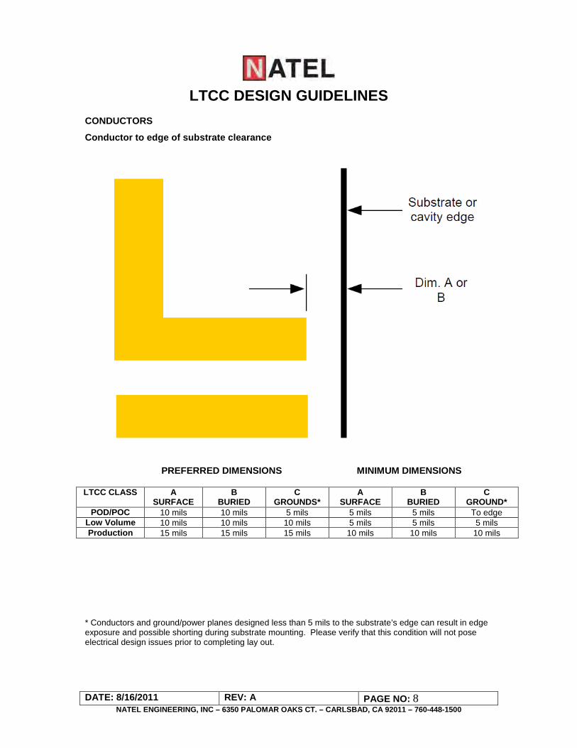
CONDUCTORS
Conductor to edge of substrate clearance
PREFERRED DIMENSIONS MINIMUM DIMENSIONS
LTCC CLASS A SURFACE
B BURIED
C GROUNDS*
A SURFACE
B BURIED
C GROUND*
POD/POC 10 mils 10 mils 5 mils 5 mils 5 mils To edge Low Volume 10 mils 10 mils 10 mils 5 mils 5 mils 5 mils Production 15 mils 15 mils 15 mils 10 mils 10 mils 10 mils
* Conductors and ground/power planes designed less than 5 mils to the substrate’s edge can result in edge exposure and possible shorting during substrate mounting. Please verify that this condition will not pose electrical design issues prior to completing lay out.
LTCC DESIGN GUIDELINES
DATE: 8/16/2011 REV: A PAGE NO: 9 NATEL ENGINEERING, INC – 6350 PALOMAR OAKS CT. – CARLSBAD, CA 92011 – 760-448-1500
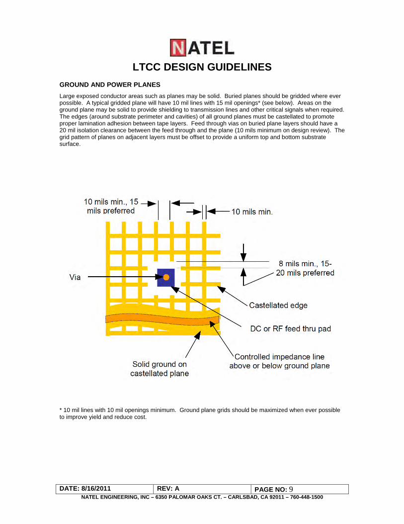
GROUND AND POWER PLANES Large exposed conductor areas such as planes may be solid. Buried planes should be gridded where ever possible. A typical gridded plane will have 10 mil lines with 15 mil openings* (see below). Areas on the ground plane may be solid to provide shielding to transmission lines and other critical signals when required. The edges (around substrate perimeter and cavities) of all ground planes must be castellated to promote proper lamination adhesion between tape layers. Feed through vias on buried plane layers should have a 20 mil isolation clearance between the feed through and the plane (10 mils minimum on design review). The grid pattern of planes on adjacent layers must be offset to provide a uniform top and bottom substrate surface.
* 10 mil lines with 10 mil openings minimum. Ground plane grids should be maximized when ever possible to improve yield and reduce cost.
LTCC DESIGN GUIDELINES
DATE: 8/16/2011 REV: A PAGE NO: 10 NATEL ENGINEERING, INC – 6350 PALOMAR OAKS CT. – CARLSBAD, CA 92011 – 760-448-1500
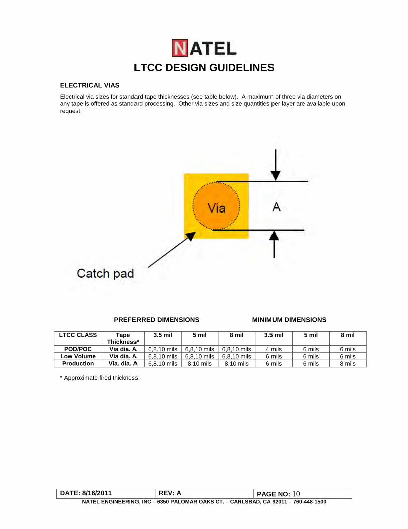
ELECTRICAL VIAS Electrical via sizes for standard tape thicknesses (see table below). A maximum of three via diameters on any tape is offered as standard processing. Other via sizes and size quantities per layer are available upon request.
PREFERRED DIMENSIONS MINIMUM DIMENSIONS
LTCC CLASS Tape Thickness*
3.5 mil 5 mil 8 mil 3.5 mil 5 mil 8 mil
POD/POC Via dia. A 6,8.10 mils 6,8,10 mils 6,8,10 mils 4 mils 6 mils 6 mils Low Volume Via dia. A 6,8.10 mils 6,8,10 mils 6,8,10 mils 6 mils 6 mils 6 mils Production Via. dia. A 6,8.10 mils 8,10 mils 8,10 mils 6 mils 6 mils 8 mils
* Approximate fired thickness.
LTCC DESIGN GUIDELINES
DATE: 8/16/2011 REV: A PAGE NO: 11 NATEL ENGINEERING, INC – 6350 PALOMAR OAKS CT. – CARLSBAD, CA 92011 – 760-448-1500
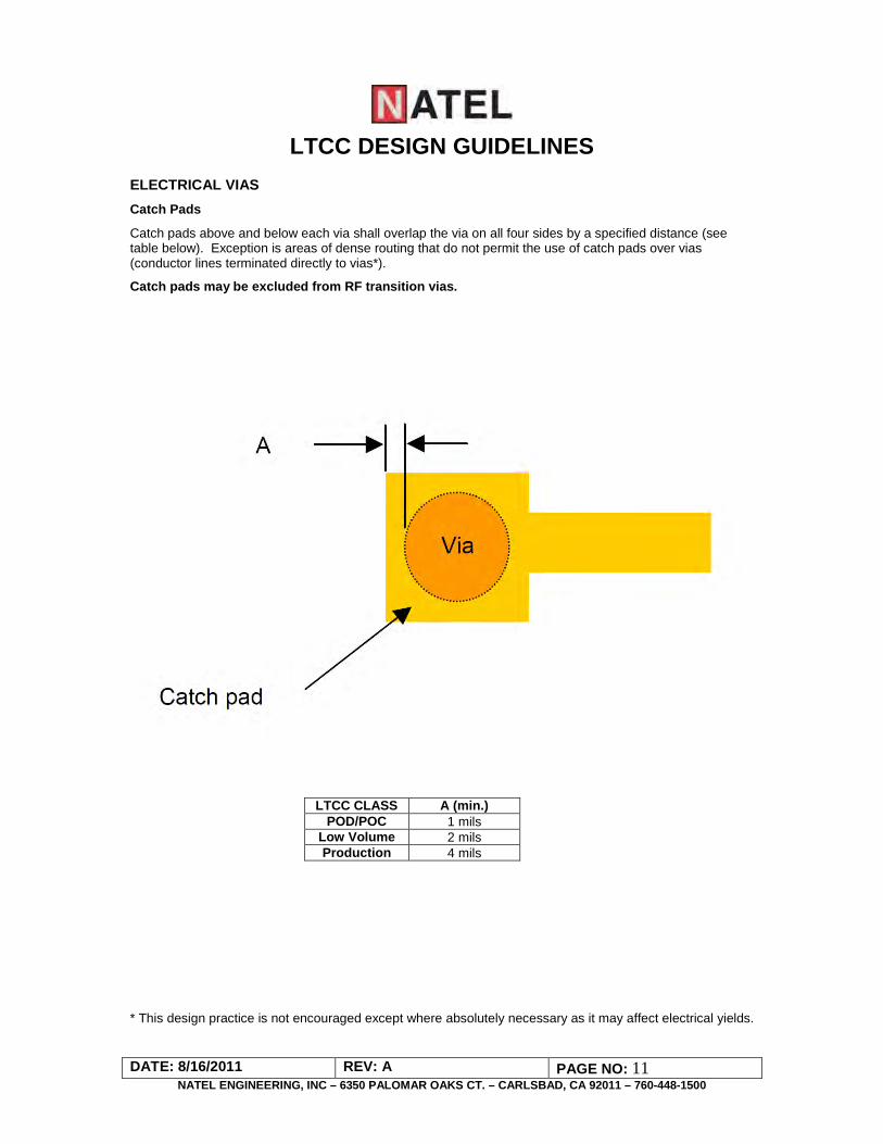
ELECTRICAL VIAS Catch Pads
Catch pads above and below each via shall overlap the via on all four sides by a specified distance (see table below). Exception is areas of dense routing that do not permit the use of catch pads over vias (conductor lines terminated directly to vias*).
Catch pads may be excluded from RF transition vias.
LTCC CLASS A (min.)
POD/POC 1 mils Low Volume 2 mils Production 4 mils
* This design practice is not encouraged except where absolutely necessary as it may affect electrical yields.
LTCC DESIGN GUIDELINES
DATE: 8/16/2011 REV: A PAGE NO: 12 NATEL ENGINEERING, INC – 6350 PALOMAR OAKS CT. – CARLSBAD, CA 92011 – 760-448-1500
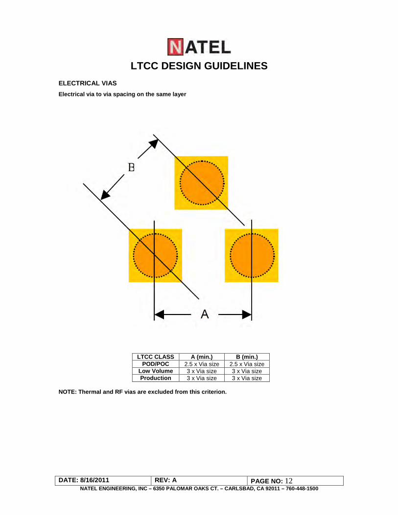
ELECTRICAL VIAS Electrical via to via spacing on the same layer
LTCC CLASS A (min.) B (min.) POD/POC 2.5 x Via size 2.5 x Via size
Low Volume 3 x Via size 3 x Via size Production 3 x Via size 3 x Via size
NOTE: Thermal and RF vias are excluded from this criterion.
LTCC DESIGN GUIDELINES
DATE: 8/16/2011 REV: A PAGE NO: 13 NATEL ENGINEERING, INC – 6350 PALOMAR OAKS CT. – CARLSBAD, CA 92011 – 760-448-1500
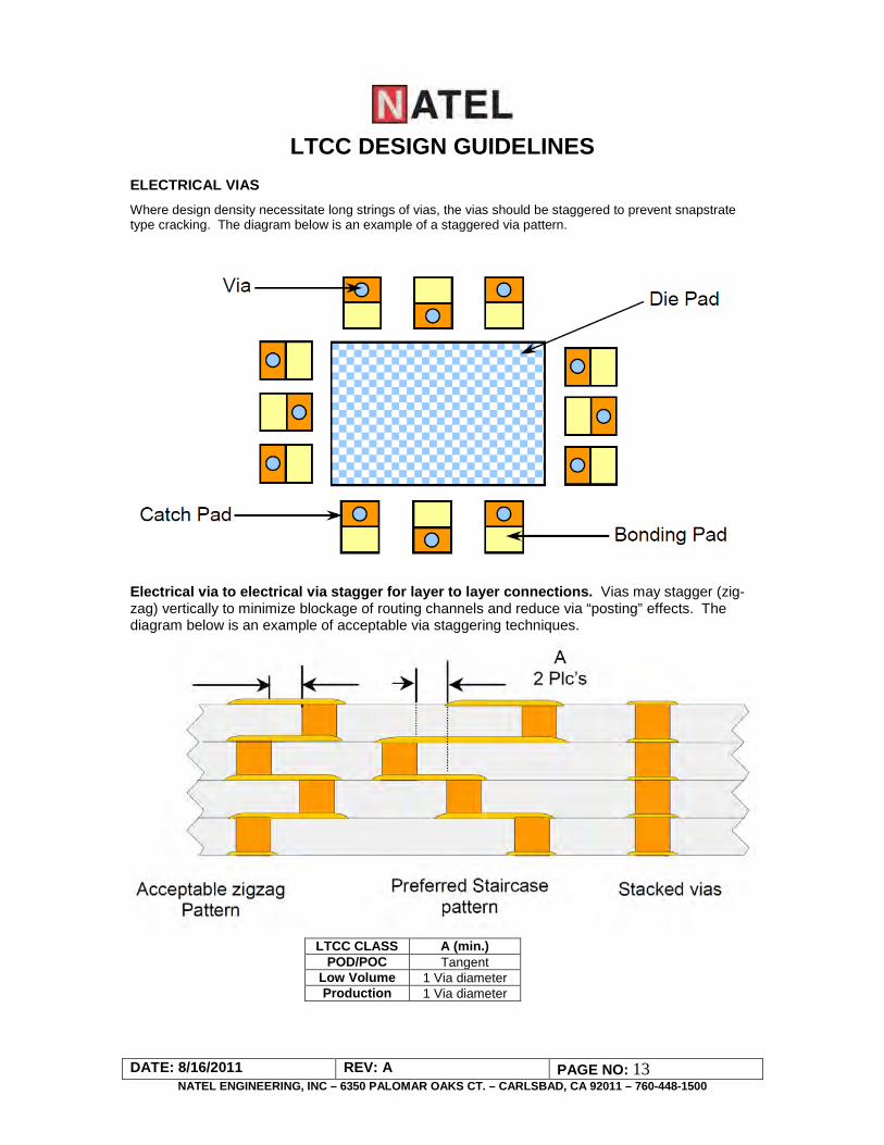
ELECTRICAL VIAS Where design density necessitate long strings of vias, the vias should be staggered to prevent snapstrate type cracking. The diagram below is an example of a staggered via pattern.
Electrical via to electrical via stagger for layer to layer connections. Vias may stagger (zig-zag) vertically to minimize blockage of routing channels and reduce via “posting” effects. The diagram below is an example of acceptable via staggering techniques.
LTCC CLASS A (min.)
POD/POC Tangent Low Volume 1 Via diameter Production 1 Via diameter
LTCC DESIGN GUIDELINES
DATE: 8/16/2011 REV: A PAGE NO: 14 NATEL ENGINEERING, INC – 6350 PALOMAR OAKS CT. – CARLSBAD, CA 92011 – 760-448-1500
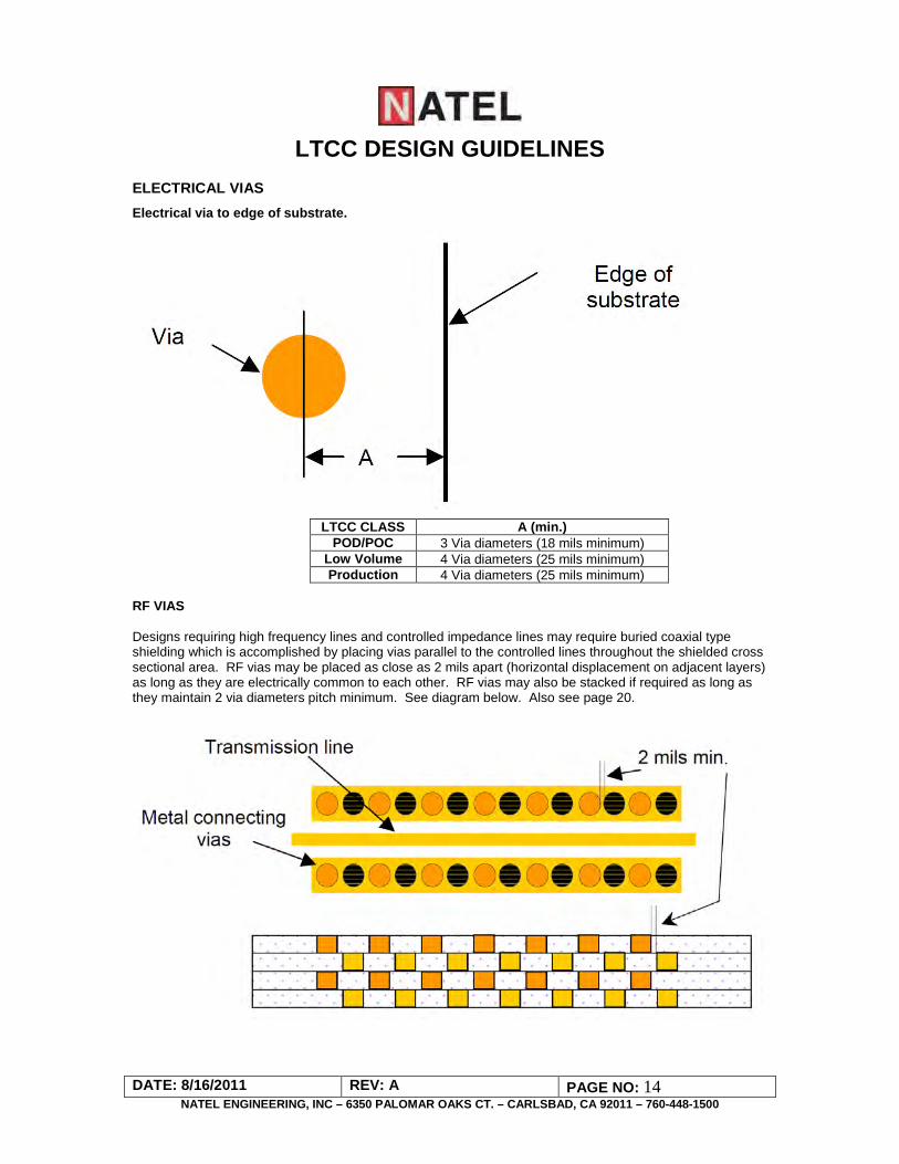
ELECTRICAL VIAS Electrical via to edge of substrate.
LTCC CLASS A (min.)
POD/POC 3 Via diameters (18 mils minimum) Low Volume 4 Via diameters (25 mils minimum) Production 4 Via diameters (25 mils minimum)
RF VIAS Designs requiring high frequency lines and controlled impedance lines may require buried coaxial type shielding which is accomplished by placing vias parallel to the controlled lines throughout the shielded cross sectional area. RF vias may be placed as close as 2 mils apart (horizontal displacement on adjacent layers) as long as they are electrically common to each other. RF vias may also be stacked if required as long as they maintain 2 via diameters pitch minimum. See diagram below. Also see page 20.

LTCC DESIGN GUIDELINES
DATE: 8/16/2011 REV: A PAGE NO: 15 NATEL ENGINEERING, INC – 6350 PALOMAR OAKS CT. – CARLSBAD, CA 92011 – 760-448-1500
THERMAL VIAS Thermal vias diameters.
LTCC CLASS A Dia. (min.)
POD/POC 4, 6, 8,10 mils Low Volume 4, 6, 8,10 mils Production 6, 8, 10 mils
Thermal via pattern
.
Via Diameter (Mils) A B C D 4 9 9 4.5 6.36 6 13.5 13.5 6.75 9.55 8 18 18 9 12.73 10 22.5 22.5 11.25 15.9 12 30 30 15 21.21 15 45 45 22.5 31.82

LTCC DESIGN GUIDELINES
DATE: 8/16/2011 REV: A PAGE NO: 16 NATEL ENGINEERING, INC – 6350 PALOMAR OAKS CT. – CARLSBAD, CA 92011 – 760-448-1500
THERMAL VIAS
The maximum thermal via array size is 250 mil, length or width. Larger thermal arrays using larger via diameters with 3 x via diameter spacing are available upon request. While the thermal vias shown in this design guide show individual cover pads a solid metal single pad covering all vias is acceptable. This approach helps spread heat reducing thermal impedance. To best reduce thermal impedance, select a via diameter that will allow for maximum packing density under the component dissipating the heat. Also try and center a via directly under a known thermal junction in the component. Stacked thermal vias are the most efficient method of reducing thermal impedance. Please keep in mind that stacked thermal via arrays may not be hermetic to helium leak testing.
Additional thermal performance and design information is available in our LTCC Design CD.
Thermal via to edge of substrate clearance.
LTCC CLASS A Minimum A Preferred POD/POC 60 mils 100 mils
Low Volume 60 mils 150 mils Production 150 mils 150 mils

LTCC DESIGN GUIDELINES
DATE: 8/16/2011 REV: A PAGE NO: 17 NATEL ENGINEERING, INC – 6350 PALOMAR OAKS CT. – CARLSBAD, CA 92011 – 760-448-1500
CAVITIES Cavity bottom conductor to cavity wall clearance.
LTCC CLASS A Minimum*
POD/POC 2.5 mils Low Volume 5 mils Production 10 mils
*Bottom conductor electrical connection can be made through cavity wall, if required, but should not exceed 25% of the wall length (preferred), 50% maximum. Castelleated metallization designs may be used to meet this requirement. Exposed/buried conductor to cavity wall clearance.
LTCC CLASS A Exposed B Buried
POD/POC 5 mils 10 mils Low Volume 5 mils 10 mils Production 15 mils 15 mils
LTCC DESIGN GUIDELINES
DATE: 8/16/2011 REV: A PAGE NO: 18 NATEL ENGINEERING, INC – 6350 PALOMAR OAKS CT. – CARLSBAD, CA 92011 – 760-448-1500
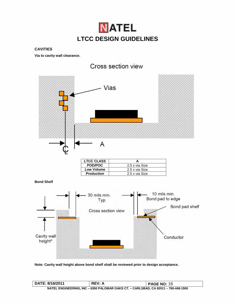
CAVITIES Via to cavity wall clearance.
LTCC CLASS A
POD/POC 2.5 x via Size Low Volume 2.5 x via Size Production 2.5 x via Size
Bond Shelf
Note: Cavity wall height above bond shelf shall be reviewed prior to design acceptance.
LTCC DESIGN GUIDELINES
DATE: 8/16/2011 REV: A PAGE NO: 19 NATEL ENGINEERING, INC – 6350 PALOMAR OAKS CT. – CARLSBAD, CA 92011 – 760-448-1500
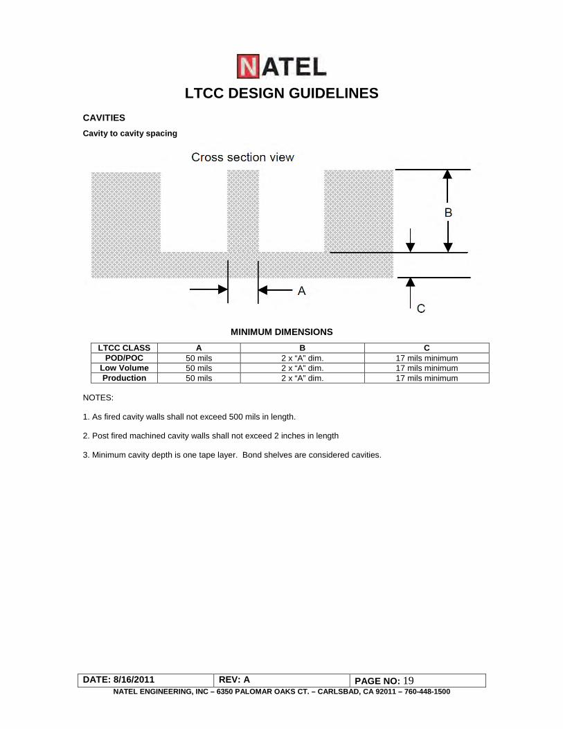
CAVITIES Cavity to cavity spacing
MINIMUM DIMENSIONS
LTCC CLASS A B C POD/POC 50 mils 2 x “A” dim. 17 mils minimum
Low Volume 50 mils 2 x “A” dim. 17 mils minimum Production 50 mils 2 x “A” dim. 17 mils minimum
NOTES: 1. As fired cavity walls shall not exceed 500 mils in length. 2. Post fired machined cavity walls shall not exceed 2 inches in length 3. Minimum cavity depth is one tape layer. Bond shelves are considered cavities.

LTCC DESIGN GUIDELINES
DATE: 8/16/2011 REV: A PAGE NO: 20 NATEL ENGINEERING, INC – 6350 PALOMAR OAKS CT. – CARLSBAD, CA 92011 – 760-448-1500
SPECIAL HIGH FREQUENCY DESIGN PROVISIONS AND SUPPORT
AVAILABLE DIELECTRIC K’s Available tape dielectric constants of 5.9 ± .15 (Ferro low loss), 7.2 (EMCA), 7.8 (Dupont).
DIMENSIONAL TOLERANCES Dielectric Z thickness tolerance is ± .0002” / layer after firing.
Via and cavity positional tolerance is ± .3% after firing.
Layer to layer alignment is ± .001”.
Cavity X, Y tolerance is ± .0025” / side.
Buried resistor tolerance 10% - 50% dependent upon design. Contact Natel applications Engineering for specific details.
VIAS AND CATCH PADS Vias may be stacked in any manner for RF transition and grounding applications.
Catch pads over vias are preferred where possible but may be omitted where electrical performance would be compromised.
GROUND PLANES Internal ground plane metallization should be gridded wherever possible. Ground planes may be made solid in the areas above, below, and adjacent to critical transmission lines.
Minimum grid pattern is .01” lines with .01” openings. A 33% opening to line ratio is preferred wherever possible.
PRECISION LINE WIDTH PROCESS CONTROL AND INSPECTION Natel will perform special measurements of critical lines and spaces when notified prior to layout and fabrication of the substrate. The design data base, mylar artwork and green fire dimensions will be closely monitored to ensure compliance to design. Critical dimensions should be recorded in a table similar to that shown in Appendix B. This table should be accompanied with a picture or diagram of the referenced measurement points.
LTCC DESIGN GUIDELINES
DATE: 8/16/2011 REV: A PAGE NO: 21 NATEL ENGINEERING, INC – 6350 PALOMAR OAKS CT. – CARLSBAD, CA 92011 – 760-448-1500
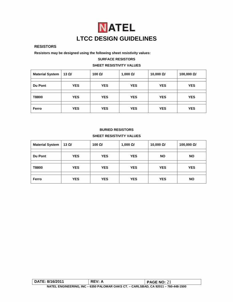
RESISTORS Resistors may be designed using the following sheet resistivity values:
SURFACE RESISTORS
SHEET RESISTIVITY VALUES
Material System 13 Ω/ 100 Ω/ 1,000 Ω/ 10,000 Ω/ 100,000 Ω/
Du Pont YES YES YES YES YES
T8800 YES YES YES YES YES
Ferro YES YES YES YES YES
BURIED RESISTORS
SHEET RESISTIVITY VALUES
Material System 13 Ω/ 100 Ω/ 1,000 Ω/ 10,000 Ω/ 100,000 Ω/
Du Pont YES YES YES NO NO
T8800 YES YES YES YES YES
Ferro YES YES YES YES NO
LTCC DESIGN GUIDELINES
DATE: 8/16/2011 REV: A PAGE NO: 22 NATEL ENGINEERING, INC – 6350 PALOMAR OAKS CT. – CARLSBAD, CA 92011 – 760-448-1500
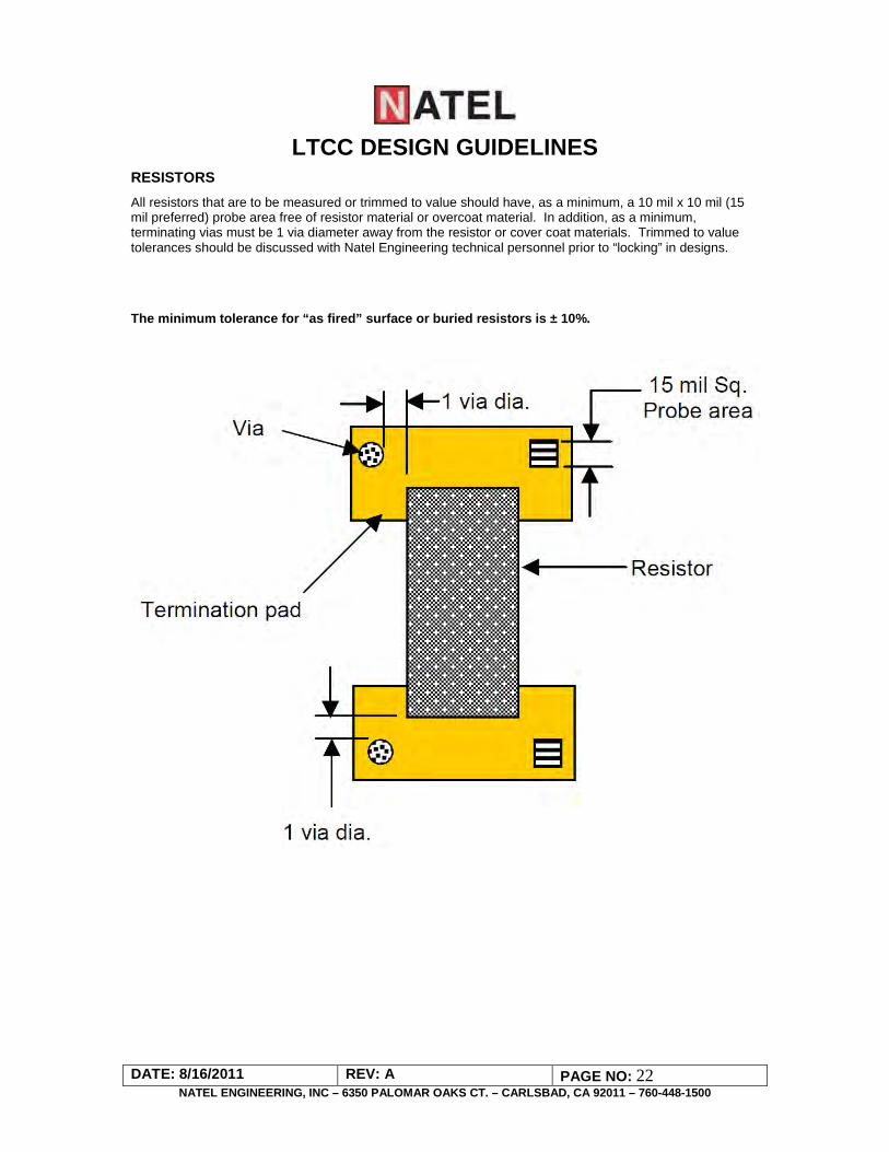
RESISTORS All resistors that are to be measured or trimmed to value should have, as a minimum, a 10 mil x 10 mil (15 mil preferred) probe area free of resistor material or overcoat material. In addition, as a minimum, terminating vias must be 1 via diameter away from the resistor or cover coat materials. Trimmed to value tolerances should be discussed with Natel Engineering technical personnel prior to “locking” in designs.
The minimum tolerance for “as fired” surface or buried resistors is ± 10%.
LTCC DESIGN GUIDELINES
DATE: 8/16/2011 REV: A PAGE NO: 23 NATEL ENGINEERING, INC – 6350 PALOMAR OAKS CT. – CARLSBAD, CA 92011 – 760-448-1500
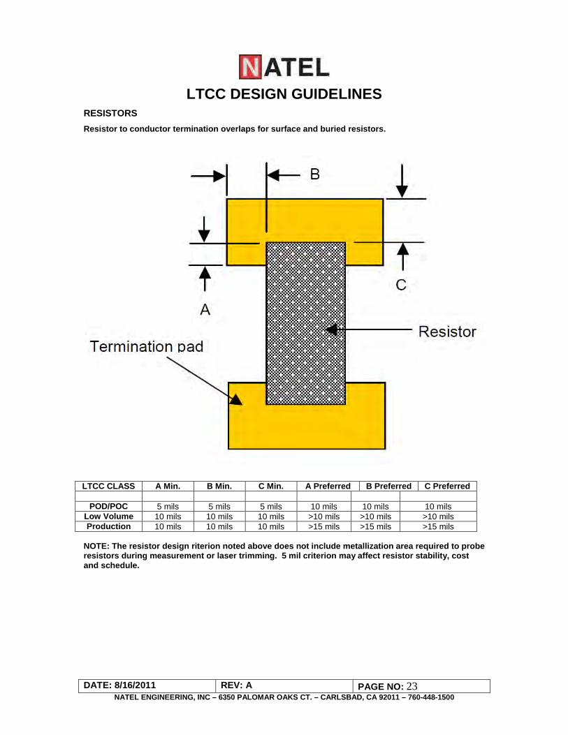
RESISTORS Resistor to conductor termination overlaps for surface and buried resistors.
LTCC CLASS A Min. B Min. C Min. A Preferred B Preferred C Preferred
POD/POC 5 mils 5 mils 5 mils 10 mils 10 mils 10 mils Low Volume 10 mils 10 mils 10 mils >10 mils >10 mils >10 mils Production 10 mils 10 mils 10 mils >15 mils >15 mils >15 mils
NOTE: The resistor design riterion noted above does not include metallization area required to probe resistors during measurement or laser trimming. 5 mil criterion may affect resistor stability, cost and schedule.

LTCC DESIGN GUIDELINES
DATE: 8/16/2011 REV: A PAGE NO: 24 NATEL ENGINEERING, INC – 6350 PALOMAR OAKS CT. – CARLSBAD, CA 92011 – 760-448-1500
RESISTORS The minimum resistor length (between conductors) and width.
The maximum buried resistor size is 70 mils x 70 mils. Buried resistor coverage shall nto exceed 15%. The maximum number of sheet resistivities per buried layer is two; maximum number of surface sheet resistivities is three.
Resistor to resistor spacing for resistors of the same sheet resistivity on the same layer. Resistors of the same sheet value with a common termination pad may abut.
LTCC CLASS A Min. B Min. C Min. A Preferred B Preferred C Preferred
POD/POC 15 mils 15 mils 30 mils 40 mils 40 mils >50 mils Low Volume 20 mils 20 mils 40 mils 40 mils 40 mils >50 mils Production 40 mils 40 mils 50 mils 40 mils 40 mils 100 mils
LTCC DESIGN GUIDELINES
DATE: 8/16/2011 REV: A PAGE NO: 25 NATEL ENGINEERING, INC – 6350 PALOMAR OAKS CT. – CARLSBAD, CA 92011 – 760-448-1500
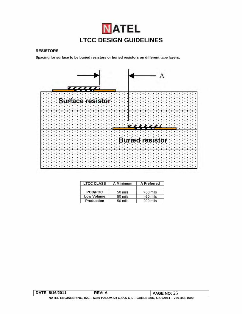
RESISTORS Spacing for surface to be buried resistors or buried resistors on different tape layers.
LTCC CLASS A Minimum A Preferred
POD/POC 50 mils >50 mils Low Volume 50 mils >50 mils Production 50 mils 200 mils

LTCC DESIGN GUIDELINES
DATE: 8/16/2011 REV: A PAGE NO: 26 NATEL ENGINEERING, INC – 6350 PALOMAR OAKS CT. – CARLSBAD, CA 92011 – 760-448-1500
RESISTORS Resistor to edge of substrate clearance
SURFACE BURIED LTCC CLASS A Minimum A Preferred
POD/POC 25 mils >50 mils
Low Volume 25 mils >50 mils Production 25 mils 200 mils

LTCC DESIGN GUIDELINES
DATE: 8/16/2011 REV: A PAGE NO: 27 NATEL ENGINEERING, INC – 6350 PALOMAR OAKS CT. – CARLSBAD, CA 92011 – 760-448-1500
RESISTORS Cover coat overlap.
LTCC CLASS A Minimum POD/POC 5 mils Low Volume 10 mils Production 10 mils

LTCC DESIGN GUIDELINES
DATE: 8/16/2011 REV: A PAGE NO: 28 NATEL ENGINEERING, INC – 6350 PALOMAR OAKS CT. – CARLSBAD, CA 92011 – 760-448-1500
CAPACITORS Capacitors may be fabricated by placing parallel plates on adjacent tape layers. Capacitance values up to 450 pico farads/in2 may be fabricated by using standard EMCA K 7 and Dupont K 7.8 tapes or 350 pico farads/in2 for Ferro K 5.9 A6 tape. Higher capacitance values up to 125,000 pico farads/in2 may be obtained by using K500 – K700 dielectrics. Buried K1000 dielectrics are in development.
The largest buried capacitor plate on standard LTCC tapes allowed is 800 mils square, but in no case shall exceed 50% of the substrate cross sectional area. The maximum plate size allowed when using K100-700 dielectrics is .28” sq. (or equivalent area, see page 28). Minimum substrate cross sections apply when using K100-700 dielectrics. Breakup capacitor plates when higher values are required, and if necessary the use of multiple tape layers is acceptable. Capacitor plates on alternate layers should overlap by 5 – 10 mils minimum on each side to eliminate registration errors that would affect electrical performance.
Please contact Natel Engineering technical staff for specific applications and new developments.

LTCC DESIGN GUIDELINES
DATE: 8/16/2011 REV: A PAGE NO: 29 NATEL ENGINEERING, INC – 6350 PALOMAR OAKS CT. – CARLSBAD, CA 92011 – 760-448-1500
CERAMIC CAPACITOR DIELECTRIC SYSTEM
FOR FERRO TAPE SYS.
2-P PROC
3-P PROC
Dielectric Type X7R NPO
Dielectric K 300 5-6
Cap Range (pf) 10-4000
1-100
Largest Pad size allowed – in2(mm2)
.076 (49)
.303 (198)
Dissipation Factor (%DF)
<2.0% <0.3%
Insulation Res. @ 100VDC
>1011 ohms
>1012 ohms
Breakdown voltage (min.)
>200 VDC
>500 VDC
Capacitance tolerance
±20% ±20%
Cap. Pad Metallizations
Silver/Gold*
Silver/ Gold*
FOR DUPONT TAPE SYS
2-P PROC
3-P PROC
X7R NPO
300 5-6
10-4000
1-100
.076 (49)
.303 (198)
<2.0% <0.3%
>1011 ohms
>1012 ohms
>200 VDC
>500 VDC
±20% ±20%
Silver/Gold*
Silver/ Gold*
FOR EMCA TAPE SYS
2-P PROC
3-P PROC
X7R NPO
300 5-6
10-4000
1-100
.076 (49)
.303 (198)
<2.0% <0.3%
>1011 ohms
>1012 ohms
>200 VDC
>500 VDC
±20% ±20%
Silver/Gold*
Silver/ Gold*
*Using silver conductors *Gold typically generates 20-30% less capacitance than silver *Typical fired thickness is .0015”
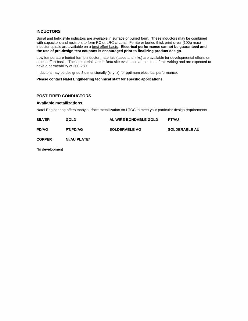
INDUCTORS Spiral and helix style inductors are available in surface or buried form. These inductors may be combined with capacitors and resistors to form RC or LRC circuits. Ferrite or buried thick print silver (100μ max) inductor spirals are available on a best effort basis. Electrical performance cannot be guaranteed and the use of pre-design test coupons is encouraged prior to finalizing product design.
Low temperature buried ferrite inductor materials (tapes and inks) are available for developmental efforts on a best effort basis. These materials are in Beta site evaluation at the time of this writing and are expected to have a permeability of 200-280.
Inductors may be designed 3 dimensionally (x, y, z) for optimum electrical performance.
Please contact Natel Engineering technical staff for specific applications.
POST FIRED CONDUCTORS
Available metallizations. Natel Engineering offers many surface metallization on LTCC to meet your particular design requirements.
SILVER GOLD AL WIRE BONDABLE GOLD PT/AU
PD/AG PT/PD/AG SOLDERABLE AG SOLDERABLE AU
COPPER NI/AU PLATE*
*In development

LTCC DESIGN GUIDELINES
DATE: 8/16/2011 REV: A PAGE NO: 31 NATEL ENGINEERING, INC – 6350 PALOMAR OAKS CT. – CARLSBAD, CA 92011 – 760-448-1500
POST FIRED CONDUCTORS Cover pad design considerations when post print and firing surface metallization over LTCC vias.
LTCC products have, on average, about a .3% variability in shrinkage during firing. If catch pads are designed too small there is a probability that the catch pad and via would not line up (overlap) during printing, resulting in an electrical open. Please see the following two diagrams for recommended cover pad dimensions when designing surface metallization routing.
COVER AD DIMENSION VS. DISTANCE FROM CENTER OF SUBSTRATE
POSSIBLE VIA LOCATION VS. DISTANCE FROM CENTER OF SUBSTRATE
LTCC DESIGN GUIDELINES
DATE: 8/16/2011 REV: A PAGE NO: 32 NATEL ENGINEERING, INC – 6350 PALOMAR OAKS CT. – CARLSBAD, CA 92011 – 760-448-1500
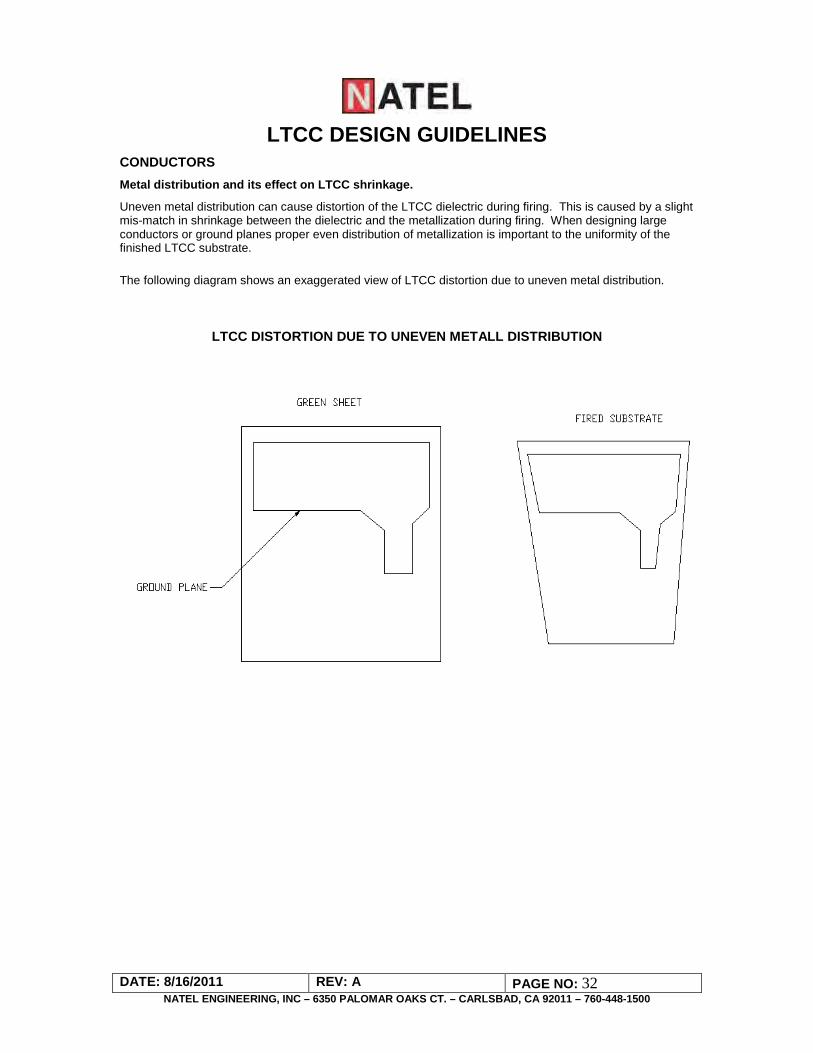
CONDUCTORS Metal distribution and its effect on LTCC shrinkage.
Uneven metal distribution can cause distortion of the LTCC dielectric during firing. This is caused by a slight mis-match in shrinkage between the dielectric and the metallization during firing. When designing large conductors or ground planes proper even distribution of metallization is important to the uniformity of the finished LTCC substrate.
The following diagram shows an exaggerated view of LTCC distortion due to uneven metal distribution.
LTCC DISTORTION DUE TO UNEVEN METALL DISTRIBUTION

LTCC DESIGN GUIDELINES
DATE: 8/16/2011 REV: A PAGE NO: 33 NATEL ENGINEERING, INC – 6350 PALOMAR OAKS CT. – CARLSBAD, CA 92011 – 760-448-1500
SOLDERING DESIGN CONSIDERATIONS Soldering of gold plated Kovar leads, pins, ring frams is standard practice in LTCC technology. Backside strength members or heat spreaders is also available. Head spreaders are available in Al-Si-C Cu-Mo-Cu, Cu-W, Molybdenum, Ni-Fe alloys and Kovar.
• Substrate overall thickness should be 40 mils minimum.
• Metal seal ring cross section should be 30 mils minimum. Ring frame corners should be radiused.
• Kovar leads and rings should be fully annealed prior to plating.
• Metal lead cross section and width should be minimized to reduce stress at the attachment site.
• Metal seal rings and leads should be plated with Ni and then Au.
• Metal seal ring aspect ratio height/width should not exceed 2.
• Preparatory metallization width should be, as a minimum, 40 mils wider than seal ring, 80 mil is preferred. Top barrier metal should overlap bottom adhesion metal 5 mils/side. Metallization corner should be radiused to prevent solder pooling and reduce stress risers.
• Provide for dielectric solder dam material around solder sites. Dielectric should overlap barrier metal 2-5 mils/side.
• Lead or pin attachment sites should be 2x the width/diameter of the lead/pin.
• Circuitry passing under the seal ring should do so at least 2-3 tape layers below the ring (8-11 mils).
LTCC DESIGN GUIDELINES
DATE: 8/16/2011 REV: A PAGE NO: 34 NATEL ENGINEERING, INC – 6350 PALOMAR OAKS CT. – CARLSBAD, CA 92011 – 760-448-1500
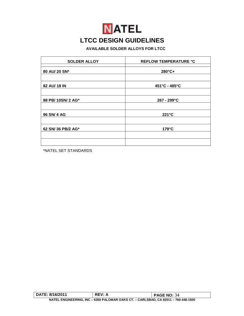
AVAILABLE SOLDER ALLOYS FOR LTCC
SOLDER ALLOY REFLOW TEMPERATURE °C
80 AU/ 20 SN* 280°C+
82 AU/ 18 IN 451°C - 485°C
88 PB/ 10SN/ 2 AG* 267 - 299°C
96 SN/ 4 AG 221°C
62 SN/ 36 PB/2 AG* 179°C
*NATEL SET STANDARDS
LTCC DESIGN GUIDELINES
DATE: 8/16/2011 REV: A PAGE NO: 35 NATEL ENGINEERING, INC – 6350 PALOMAR OAKS CT. – CARLSBAD, CA 92011 – 760-448-1500
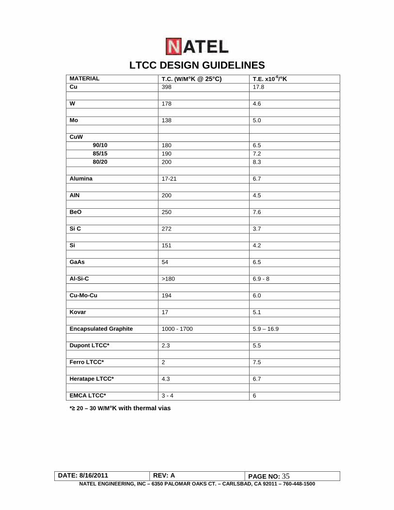
MATERIAL T.C. (W/M°K @ 25°C) T.E. x10-6/°K Cu 398 17.8 W 178 4.6 Mo 138 5.0 CuW
90/10 180 6.5 85/15 190 7.2 80/20 200 8.3
Alumina 17-21 6.7 AIN 200 4.5 BeO 250 7.6 Si C 272 3.7 Si 151 4.2 GaAs 54 6.5 Al-Si-C >180 6.9 - 8 Cu-Mo-Cu 194 6.0 Kovar 17 5.1 Encapsulated Graphite 1000 - 1700 5.9 – 16.9 Dupont LTCC* 2.3 5.5 Ferro LTCC* 2 7.5 Heratape LTCC* 4.3 6.7 EMCA LTCC* 3 - 4 6
*≥ 20 – 30 W/M°K with thermal vias

LTCC DESIGN GUIDELINES
DATE: 8/16/2011 REV: A PAGE NO: 36 NATEL ENGINEERING, INC – 6350 PALOMAR OAKS CT. – CARLSBAD, CA 92011 – 760-448-1500
PROPERTY DUPONT 951 FERROR A6 FERRO A6-B EMCA T8800 HERATAPE CT700*
Color Blue White Black Blue Blue
Available Fired Thickness (mils)
3.7, 5.2, 8.2 3.7, 7.4 3.3, 6.7 3.5-10 3.6, 5.7, 7.9
Dielectric Constant (K) 7.28 5.9 6.5 7.27 7.9
Loss Tangent .15% <.2% <.5% <.2% <.2%
Mwave Insertion Loss(DB/in) @10Ghz
<.6 .18 <.35 <.5 -
Insulation Resistance >1012 Ohms >1012 Ohms >1012 Ohms >1012 Ohms >1012 Ohms
Breakdown Voltage >1000 V/Mil >900 V/Mil >1000 V/Mil >1000 V/Mil >1000 V/Mil
Electrolytic Leak Current - <1μ-amp/cm2 <1μ-amp/cm2 - -
Flexural strength** 207 MPa >124 MPa >124 MPa >276 MPa -
Young’s Modulus (fired) 103 GPa 82 GPa 95 GPa 187 GPa -
Poisson Ratio .17 - - - -
Fired Density 3.1 gm/cc 2.5 gm/cc 2.5 gm/cc 3.06 3.1
Surface Roughness <10 μ in <15 μ in <15 μ in <15 μ in <22 μ in
Chamber Conforms to setter
Conforms to setter
Conforms to setter
Conforms to setter
Conforms to setter
Shrinkage
X, Y 12.7% ± .2% 14.8% ± .2% 14.5% ± .2% 13.3% ± .2% 15% ± .2%
Z 15% ± .2% 25% ± .2% 35% ± .2% 14% ± .2% 25% ± .2%
Metallizations Au/Ag – Ag - Au
Au/Ag – Ag - Au
Au/Ag – Ag - Au
Au/Ag – Ag - Au
Au/Ag – Ag - Au
*Available from C-MAC GmbH (Villingen Germany) with “0 shrink process.” **3 point MOR test - 850°C firing temperature
LTCC DESIGN GUIDELINES
DATE: 8/16/2011 REV: A PAGE NO: 37 NATEL ENGINEERING, INC – 6350 PALOMAR OAKS CT. – CARLSBAD, CA 92011 – 760-448-1500
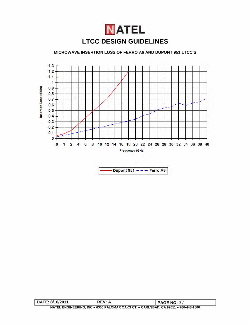
MICROWAVE INSERTION LOSS OF FERRO A6 AND DUPONT 951 LTCC’S

LTCC DESIGN GUIDELINES
DATE: 8/16/2011 REV: A PAGE NO: 38 NATEL ENGINEERING, INC – 6350 PALOMAR OAKS CT. – CARLSBAD, CA 92011 – 760-448-1500
DATABASE AND DOCUMENTATION CONVENTIONS FOR LTCC DESIGNS
DOCUMENTATION PACKAGE
Please provide Natel Engineering the following design documentation package prior to fabrication:
1. Gerber artwork database in 1-up format.
Design size should be 1:1
Aperture list
Readme text file with all pertinent design information (no of layers, metals via sizes, etc.)
2. Artwork layer plots
3. Substrate top level drawing with dimensions and side view alyering scheme.
4. Product specification
5. Electrical net list.
Design/Artwork packages may be sent to Natel Engineering at:
6350 Palomar Oaks Ct.
Carlsbad, CA 92011
Please send data in .zip format.
Drawing templates and this design guide are available for downloading upon request.

LTCC DESIGN GUIDELINES
DATE: 8/16/2011 REV: A PAGE NO: 39 NATEL ENGINEERING, INC – 6350 PALOMAR OAKS CT. – CARLSBAD, CA 92011 – 760-448-1500
ELECTRONIC DESIGN CRITERION
Preferred Design Format
Natel Engineering’s preferred method of receiving data for artwork generation is in Gerber format. This is als oteh least costly because it eliminates conversion. DXF or GDS II formats may be submitted for layout at additional cost. An additional week of lead time should be planned in the schedule if DXF or GDS II formats are used. Please contact our marketing department for design charges and lead times.
Basic LTCC Layout Considerations All designs should be submitted in one up configuration! Natel will step and repeat all designs to best fit internal processing requirements.
All designs should include a substrate outline with all design layers using a common origin. This convention holds true for Gerber, AutoCad and GDS II designs.
All vias should be filled as flashes.
Cavity areas should be shown on its associated via layer as an outline. Please use a 5 mil decode for this structure wit the outermost edge of the decode defining the cavity boundary. Please do not use overlappy polygons, use a single boundary.
All conductors should be rastor filled using Gerber type 274X whenever possible.
Please do not include dielectric layers as part of an LTCC design. Substrate outline, vias, cavity outlines and conductors are the only required design layers.
Required Design Information Please include an aperture list and a readme.txt file to facilitate loading of the design file into our CAD system. Required information in aperture list or readme file are:
a. Format – Gerber RS274, 274x, Fire 9xxx, etc.
b. Zero suppression – Leading, trailing, or none.
c. Type – Absolute or incremental
d. Digits – Integer/Decimal – 2/4, 2/5, etc.
e. Units – English or Metric
f. Decode number, type, and size (do not use decodes of zero). Please identify and describe any custom decodes clearly.
g. Part drawing or sketch defining all required dimensions and specifications. Please specify materials to be used in part fabrication.

LTCC DESIGN GUIDELINES
DATE: 8/16/2011 REV: A PAGE NO: 40 NATEL ENGINEERING, INC – 6350 PALOMAR OAKS CT. – CARLSBAD, CA 92011 – 760-448-1500
LAYER CONVENTION FOR LTCC DESIGNS SAMPLE 7LAYER SUBSTRATE
CAD DESIGN LAYER CONVENTION FOR LTCC
(Sample part; for reference only)
Tape Layer Tape Thickness Via Designation Via Diameters Cond Designation Description
1 Back M1B Ground
1 Top 3.7 mil via1 8 mil M1 Signal
2 5.5 mil via2 6 mil M2 VDD
3 5.5 mil via3 6&8 mil M3 VCC
4 8.3 mil via4 10 mil M4 RF
5 3.7 mil via5 8 mil M5 Ground
6 3.7 mil via6 8 mil M6 Signal
7 3.7 mil via7 8 mil M7 Top Pads Multiple conductors on the same layer should be identified with a suffix -1, -2, -3, … etc. For example: The second conductor (or resistor print) on the back side of tape layer 1 would be identified as M1B-1. The second conductor on tape layer 7 would be M7-2. Cavities should reside on via layers as outlines and be identified by layer. Please show cavities in substrate cross section stackup.
LTCC DESIGN GUIDELINES
DATE: 8/16/2011 REV: A PAGE NO: 41 NATEL ENGINEERING, INC – 6350 PALOMAR OAKS CT. – CARLSBAD, CA 92011 – 760-448-1500
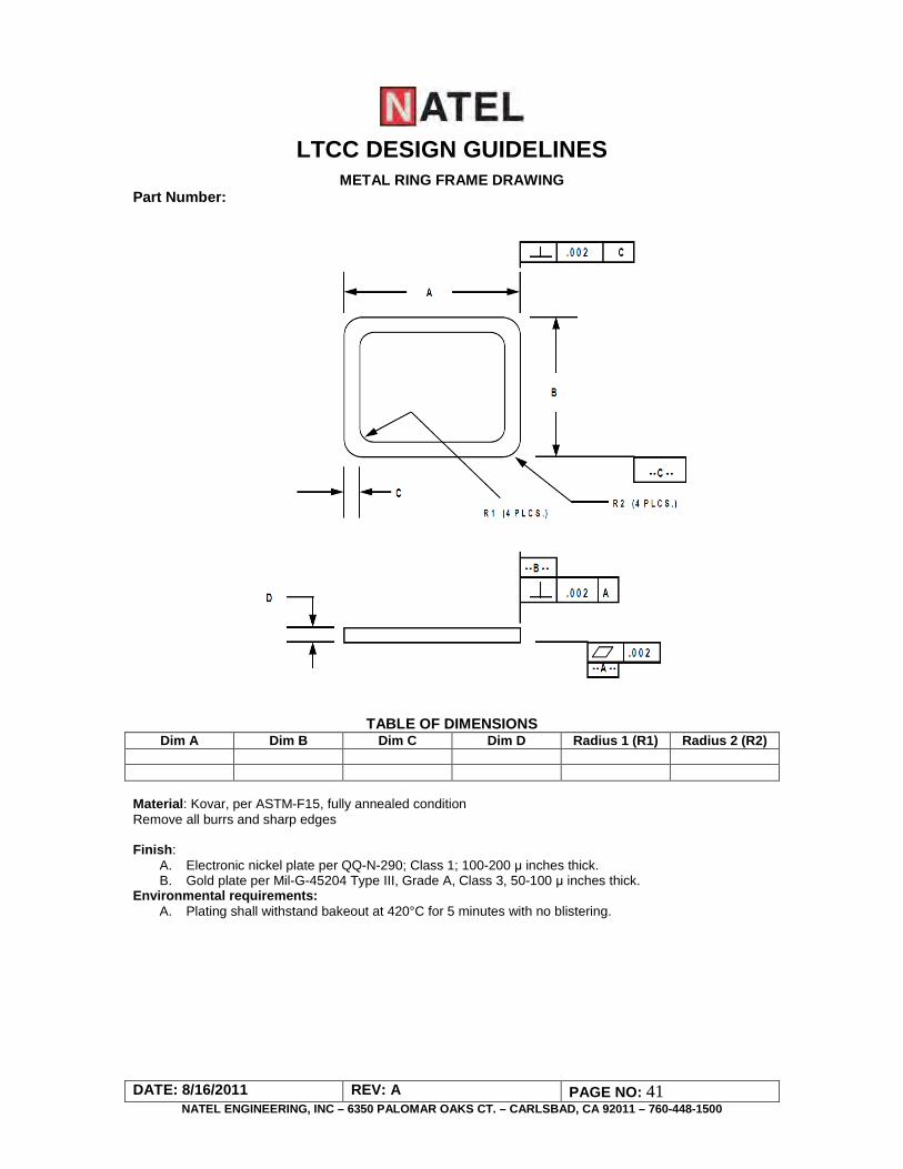
METAL RING FRAME DRAWING Part Number:
TABLE OF DIMENSIONS Dim A Dim B Dim C Dim D Radius 1 (R1) Radius 2 (R2)
Material: Kovar, per ASTM-F15, fully annealed condition Remove all burrs and sharp edges Finish:
A. Electronic nickel plate per QQ-N-290; Class 1; 100-200 μ inches thick. B. Gold plate per Mil-G-45204 Type III, Grade A, Class 3, 50-100 μ inches thick.
Environmental requirements: A. Plating shall withstand bakeout at 420°C for 5 minutes with no blistering.

LTCC DESIGN GUIDELINES
DATE: 8/16/2011 REV: A PAGE NO: 42 NATEL ENGINEERING, INC – 6350 PALOMAR OAKS CT. – CARLSBAD, CA 92011 – 760-448-1500
DESIGN CRITICAL DIMENSION TABLE Dim. Ref. Area Design Layer Dimension Tolerance A B C D E F G H I J K L M N O P Q R S T U V W X Y Z

LTCC DESIGN GUIDELINES
DATE: 8/16/2011 REV: A PAGE NO: 43 NATEL ENGINEERING, INC – 6350 PALOMAR OAKS CT. – CARLSBAD, CA 92011 – 760-448-1500
NOTES