Embed Size (px)
Citation preview

Semiconductor Physics, Quantum Electronics & Optoelectronics, 2013. V. 16, N 2. P. 216-219.
© 2013, V. Lashkaryov Institute of Semiconductor Physics, National Academy of Sciences of Ukraine
216
PACS 78.20.-e, 82.33.Xj
Low-temperature deposition of silicon dioxide films in high-density plasma
A. Yasunas1, D. Kotov1,2, V. Shiripov2, U. Radzionay1
1Belarusian State University of Informatics and Radioelectronics, 6, P. Brovky, 220013 Minsk, Republic of Belarus, e-mail: [email protected], 7-202, Selitskogo str., 220075 Minsk, Republic of Belarus
Abstract. One of the basic operations in the LED (light-emitting diode) chip fabrication technique is formation of dielectric coatings for the purpose of insulation and surface passivation of the LED structure. Oxides and nitrides of silicon obtained by physical or chemical vapor deposition techniques can act as such a coating. Low conformity of physical vapor deposition techniques limits the possibility of their application in a number of cases at LED mesostructures passivation. This work represents the results of experiments on silicon dioxide dielectric films deposition in the inductive coupledplasma under different operation conditions. The findings prove the possibility of low-temperature deposition of thick silicon dioxide films with high conformality by the HDPCVD (high-density plasma chemical vapor deposition) technique.
Keywords: inductive coupled plasma, HDPCVD, TEOS, silicon dioxide, mesa construction.
Manuscript received 12.12.12; revised version received 16.01.13; accepted for publication 19.03.13; published online 25.06.13.
1. Introduction
Glow discharge plasma in reactive gases at a low pressure is used for coatings, in microelectronics and LED technology.
The main advantage of plasma-enhanced reactionsis they occur at temperatures much lower than those in thermal reactions. Thermodynamic non-equilibrium of decomposition processes in gas discharge allows deposition of amorphous and polycrystalline films at much lower temperatures than in similar processes of chemical vapor deposition in which a thermal decomposition of the reaction gas is going on.
The deposition temperature of these films is usually lower than 420 °C, and in high-density plasma is lower than 100 °C, which allows depositing films on substrates that don’t have the necessary stability for thermal processes and significantly extends the technological possibilities.
Besides, the chemical reaction activation by plasma allows to increase the rate of deposition and to obtain films of the unique structure [1].
Into the number of extra edges provided by thedielectric layer deposition process in high-density plasma, it’s necessary to include the high quality of deposition material (from the viewpoint of stoichiometry, density, content of foreign matter –hydrogen, hydroxyl groups, metal atoms, charge characteristics, etc.), which exceeds the quality of layersbeing obtained when using other types of plasma deposition methods.
In high-density plasma chemical vapor deposition (HDPCVD) processes, by increasing the ionization degree of the initial reagents and reducing the operation pressure in the chamber, the ratio of the flow of charged particles to the flow of neutral particles onto substrates two orders of magnitude higher than in the plasma-enhanced chemical vapor deposition (PECVD) processes [2].

Semiconductor Physics, Quantum Electronics & Optoelectronics, 2013. V. 16, N 2. P. 216-219.
© 2013, V. Lashkaryov Institute of Semiconductor Physics, National Academy of Sciences of Ukraine
217
It allows to carry out the deposition process at a lower temperature of the substrate surface.
2. Experimental
The PECVD of SiO2 was carried out in a vacuum chamber installation УРМЗ 3.279.050 using the inductively coupled high-density plasma source of the 240-mm diameter operating at 13.56 MHz frequency. High-vacuum pumping was carried out by a vapor-diffusion pump operating with a pair of mechanical pumps, a double rotary (Roots pump) and rotary vane with oil seal. The initial pressure in the chamber was not
worse than Pa103 3 . The vapor supply of the reactive substance – tetraetoxisilan (TEOS) – was carried out byusing a bubbler, the carrier gas was argon. The operation pressure in the experiments was within the range from 1 to 10 Pa. The TEOS tank temperature was 21 °С. The main goal of the experiments was to obtain a quality film of silicon dioxide at a substrate temperature not higher than 200 °C. As a main criterion of film quality we chose the refractive index that for stoichiometric silicon dioxide is 1.46. The measurements of the refractive index were performed using ellipsometry.
The process was carried out in a cylindrical chamber where the ICP source, the substrate holder and gas distribution were placed (see Fig. 1). Being enhanced by plasma deposition, a coating film was formed at all surfaces in contact with the plasma. The increase in the deposition rate can be achieved by the increase in the vapor flow rate in the deposition area.When distancing the substrate from the gas supply area,the amount of substance entering a reaction in the free volume of the reactor increases, and a vapor-gas mixture depletes, which leads to a decrease in the rate of deposition on the substrate. During the experiments, it was noted that the main area of silicon oxide crystal precipitationis observed at the boundary of plasma formation and at a distance of approximately 5 cm from the vapor-gas mixture supply.
As the intensive reaction of silica formation starts directly when the TEOS vapor gets into the plasma, so the vapor-gas mixture was injected into plasma in front of the substrate. For this purpose a cylindrical Teflon housing was introduced into the design of the reactor, which separates the area of plasma formation from thevapor reagent transfer area. This design allowedachieving of the highest deposition rate.
The research of RF power transferred influence to the discharge on the film quality and its deposition rate was carried out. In these experiments, the distance between the antenna system and the sample was 15 cm.The flow rate ratio of argon to oxygen consumption was equal to 3. The substrate holder wasn’t subjected to heating; the temperature during the deposition process didn’t exceed 200 °C. The resulting dependence of the deposition rate and the refractive index are shown in Fig. 2. One can see that the reduction in power being put
into the lower than 800 W discharge increases the refractive index. It shows that the generated silicon oxide isn’t stoichiometric, and silicon, which is a composite of the film, is not completely oxidized. An increase in operating power over 800 W did not change the properties of the coatings. The deposition rate reducing with increasing the operation power can be explained by the fact that under oxidizing silicon has lower density, and its thickness is higher for the same reagent consumption. It is also confirmed by the deposition rate stabilization at high powers.
Also, the silicon oxide films deposition with various flow ratios of argon and oxygen into the chamber were carried out (see Fig. 2). The flow ratio of argon to oxygen flow varied from 1 up to 10; besides the argon flow rate was constant and equal to 110 sccm. The pressure in the chamber varied between 2.5 to 5 Pa. We see that the reduction of oxygen in the vapor-gas mixturelinearly increases the growth rate of the film, with the ratio f(Ar) / f(O2) more than four. In the same conditions,the refractive index n was beyond the ellipsometer measurements and exceeded 1.52. With the flow ratio 3 ≤ f(Ar) / f(O2) ≤ 4 the deposition rate increased, and the refraction index was within 1.46 ≤ n ≤ 1.47, whatshows good quality of the formed film. With the ratio f(Ar) / f(O2) ≥ 3, the deposition rate is more complex: it decreases to the ratio of two, then it increases within the ratio of 1.25…1.75 and then decreases again. In this case, the refractive index is constantly decreasing, what indicates the porosity of the formed film (see Fig. 4).Such a character of the rate change can be also explained by the same porosity of the film, and its volume increase at the same TEOS flow rate. The resulting film porosityis obvious at the pictures of the scanning electron microscope (SEM).
plasma
MFC
MFC
13 56 MHz .PowersSuply
TEOS
Vacuum pump
substrateholder
substrate
Ar O2
Fig. 1. Reactor configuration for silicon dioxide deposition by HDPCVD method from a mixture of TEOS and O2 (MFC –mass flow controller).
Semiconductor Physics, Quantum Electronics & Optoelectronics, 2013. V. 16, N 2. P. 216-219.
© 2013, V. Lashkaryov Institute of Semiconductor Physics, National Academy of Sciences of Ukraine
218
Fig. 2. The dependence of the refractive index and SiOx film growth rate on the ratio of Ar and O2 in the operation mixture.
Fig. 3. The dependence of the SiO2 film growth rate and refractive index from the input RF power, with the ratio off(Ar) / f(O2) = 3.
a
b
Fig. 4. SEM image of SiO2 film on the glass: (a) f(Ar) / f(O2) = 3, (b) f(Ar) / f(O2) = 2.
a
b
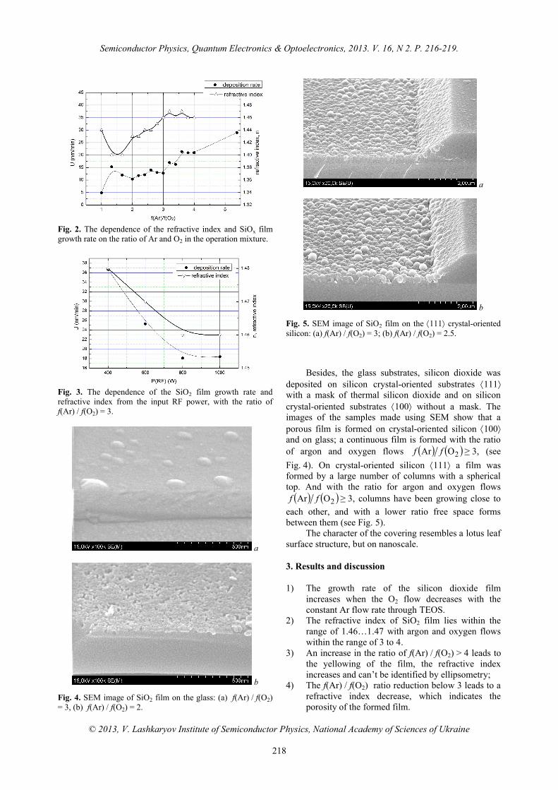
Fig. 5. SEM image of SiO2 film on the 111 crystal-oriented silicon: (a) f(Ar) / f(O2) = 3; (b) f(Ar) / f(O2) = 2.5.
Besides, the glass substrates, silicon dioxide was deposited on silicon crystal-oriented substrates 111with a mask of thermal silicon dioxide and on silicon crystal-oriented substrates 100 without a mask. The images of the samples made using SEM show that aporous film is formed on crystal-oriented silicon 100and on glass; a continuous film is formed with the ratioof argon and oxygen flows 2OAr ff ≥ 3, (see
Fig. 4). On crystal-oriented silicon 111 a film was formed by a large number of columns with a spherical top. And with the ratio for argon and oxygen flows 2OAr ff ≥ 3, columns have been growing close to
each other, and with a lower ratio free space forms between them (see Fig. 5).
The character of the covering resembles a lotus leaf surface structure, but on nanoscale.
3. Results and discussion
1) The growth rate of the silicon dioxide film increases when the O2 flow decreases with theconstant Ar flow rate through TEOS.
2) The refractive index of SiO2 film lies within the range of 1.46…1.47 with argon and oxygen flows within the range of 3 to 4.
3) An increase in the ratio of f(Ar) / f(O2) > 4 leads to the yellowing of the film, the refractive index increases and can’t be identified by ellipsometry;
4) The f(Ar) / f(O2) ratio reduction below 3 leads to a refractive index decrease, which indicates the porosity of the formed film.

Semiconductor Physics, Quantum Electronics & Optoelectronics, 2013. V. 16, N 2. P. 216-219.
© 2013, V. Lashkaryov Institute of Semiconductor Physics, National Academy of Sciences of Ukraine
219
5) With the operation power 800 to 1000 W thedeposition rate and refractive index remain unchanged, a further reduction in power leads tothe refractive index and the growth rate increase, which is associated with silicon being underoxidation.
4. Conclusion
The analysis of the experimental results shows that the method of dielectrics deposition in high-density plasma allows to deposit stoichiometric silicon dioxide films at
the substrate temperature 200 °C, and at the same time stoichiometry can be controlled by varying the reaction components ratio.
References
1. Putria M.G., Plasma Technologies inNanoelectronics. Handbook. MIET Publ. House, Moscow, 2009 (in Russian).
2. Gromov D.G., Metallization in Systems with Nanosize Elements. Handbook. MIET Publ. House, Moscow, 2011 (in Russian).