Embed Size (px)
Citation preview
Low-temperature, site selective graphitization of SiC via ion implantationand pulsed laser annealingMaxime G. Lemaitre, Sefaattin Tongay, Xiaotie Wang, Dinesh K. Venkatachalam, Joel Fridmann et al. Citation: Appl. Phys. Lett. 100, 193105 (2012); doi: 10.1063/1.4707383 View online: http://dx.doi.org/10.1063/1.4707383 View Table of Contents: http://apl.aip.org/resource/1/APPLAB/v100/i19 Published by the American Institute of Physics. Related ArticlesScreened hybrid density functional study on Sr2Nb2O7 for visible light photocatalysis Appl. Phys. Lett. 100, 181903 (2012) Role of donor-acceptor complexes and impurity band in stabilizing ferromagnetic order in Cu-doped SnO2 thinfilms Appl. Phys. Lett. 100, 172402 (2012) Single atom identification by energy dispersive x-ray spectroscopy Appl. Phys. Lett. 100, 154101 (2012) Modification of the electrical properties of poly(3,4-ethylenedioxythiophene) doped with poly(4-styrenesulfonate)upon doping of ZnO nanoparticles of different content J. Appl. Phys. 111, 073712 (2012) S doping effect on the properties of double perovskite La2FeMoO6 Appl. Phys. Lett. 100, 132404 (2012) Additional information on Appl. Phys. Lett.Journal Homepage: http://apl.aip.org/ Journal Information: http://apl.aip.org/about/about_the_journal Top downloads: http://apl.aip.org/features/most_downloaded Information for Authors: http://apl.aip.org/authors
Downloaded 13 May 2012 to 150.203.181.159. Redistribution subject to AIP license or copyright; see http://apl.aip.org/about/rights_and_permissions
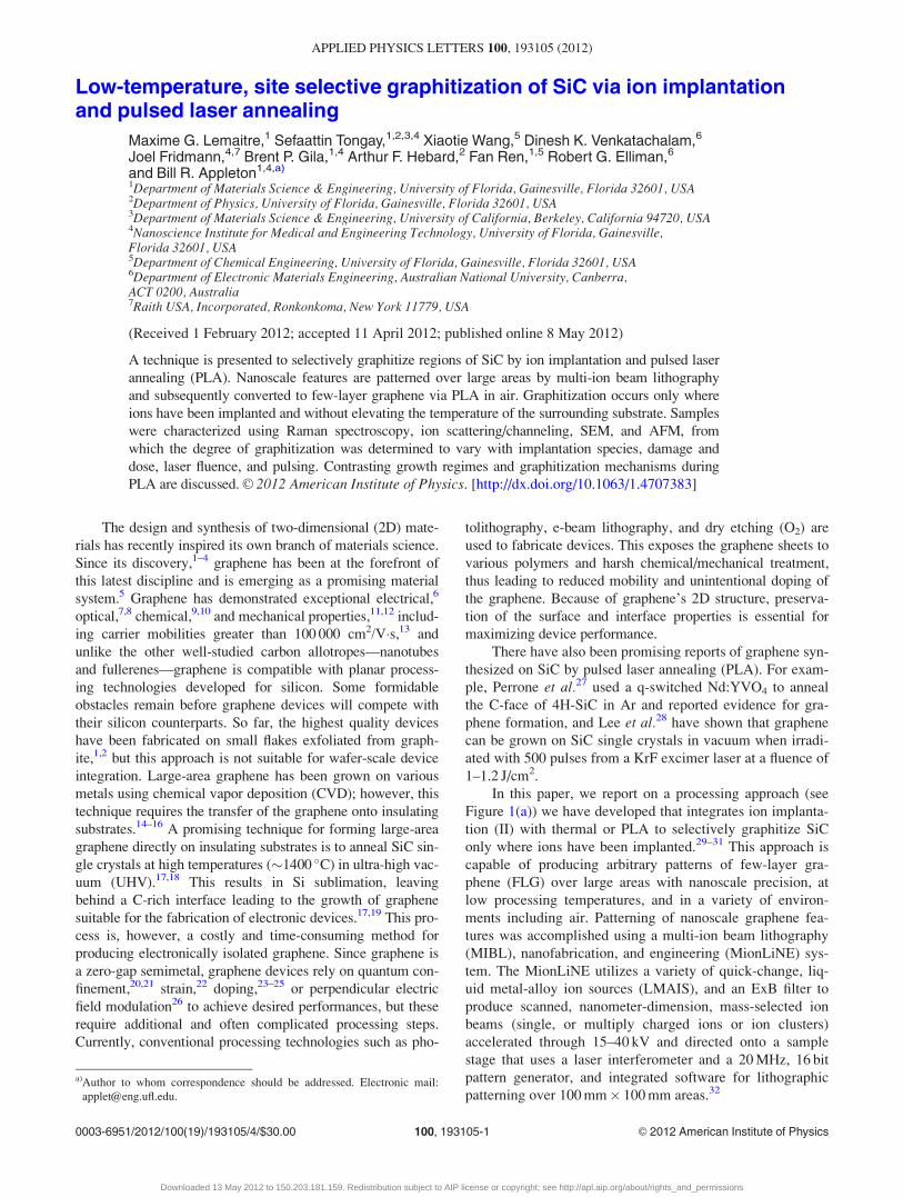
Low-temperature, site selective graphitization of SiC via ion implantationand pulsed laser annealing
Maxime G. Lemaitre,1 Sefaattin Tongay,1,2,3,4 Xiaotie Wang,5 Dinesh K. Venkatachalam,6
Joel Fridmann,4,7 Brent P. Gila,1,4 Arthur F. Hebard,2 Fan Ren,1,5 Robert G. Elliman,6
and Bill R. Appleton1,4,a)
1Department of Materials Science & Engineering, University of Florida, Gainesville, Florida 32601, USA2Department of Physics, University of Florida, Gainesville, Florida 32601, USA3Department of Materials Science & Engineering, University of California, Berkeley, California 94720, USA4Nanoscience Institute for Medical and Engineering Technology, University of Florida, Gainesville,Florida 32601, USA5Department of Chemical Engineering, University of Florida, Gainesville, Florida 32601, USA6Department of Electronic Materials Engineering, Australian National University, Canberra,ACT 0200, Australia7Raith USA, Incorporated, Ronkonkoma, New York 11779, USA
(Received 1 February 2012; accepted 11 April 2012; published online 8 May 2012)
A technique is presented to selectively graphitize regions of SiC by ion implantation and pulsed laser
annealing (PLA). Nanoscale features are patterned over large areas by multi-ion beam lithography
and subsequently converted to few-layer graphene via PLA in air. Graphitization occurs only where
ions have been implanted and without elevating the temperature of the surrounding substrate. Samples
were characterized using Raman spectroscopy, ion scattering/channeling, SEM, and AFM, from
which the degree of graphitization was determined to vary with implantation species, damage and
dose, laser fluence, and pulsing. Contrasting growth regimes and graphitization mechanisms during
PLA are discussed. VC 2012 American Institute of Physics. [http://dx.doi.org/10.1063/1.4707383]
The design and synthesis of two-dimensional (2D) mate-
rials has recently inspired its own branch of materials science.
Since its discovery,1–4 graphene has been at the forefront of
this latest discipline and is emerging as a promising material
system.5 Graphene has demonstrated exceptional electrical,6
optical,7,8 chemical,9,10 and mechanical properties,11,12 includ-
ing carrier mobilities greater than 100 000 cm2/V�s,13 and
unlike the other well-studied carbon allotropes—nanotubes
and fullerenes—graphene is compatible with planar process-
ing technologies developed for silicon. Some formidable
obstacles remain before graphene devices will compete with
their silicon counterparts. So far, the highest quality devices
have been fabricated on small flakes exfoliated from graph-
ite,1,2 but this approach is not suitable for wafer-scale device
integration. Large-area graphene has been grown on various
metals using chemical vapor deposition (CVD); however, this
technique requires the transfer of the graphene onto insulating
substrates.14–16 A promising technique for forming large-area
graphene directly on insulating substrates is to anneal SiC sin-
gle crystals at high temperatures (�1400 �C) in ultra-high vac-
uum (UHV).17,18 This results in Si sublimation, leaving
behind a C-rich interface leading to the growth of graphene
suitable for the fabrication of electronic devices.17,19 This pro-
cess is, however, a costly and time-consuming method for
producing electronically isolated graphene. Since graphene is
a zero-gap semimetal, graphene devices rely on quantum con-
finement,20,21 strain,22 doping,23–25 or perpendicular electric
field modulation26 to achieve desired performances, but these
require additional and often complicated processing steps.
Currently, conventional processing technologies such as pho-
tolithography, e-beam lithography, and dry etching (O2) are
used to fabricate devices. This exposes the graphene sheets to
various polymers and harsh chemical/mechanical treatment,
thus leading to reduced mobility and unintentional doping of
the graphene. Because of graphene’s 2D structure, preserva-
tion of the surface and interface properties is essential for
maximizing device performance.
There have also been promising reports of graphene syn-
thesized on SiC by pulsed laser annealing (PLA). For exam-
ple, Perrone et al.27 used a q-switched Nd:YVO4 to anneal
the C-face of 4H-SiC in Ar and reported evidence for gra-
phene formation, and Lee et al.28 have shown that graphene
can be grown on SiC single crystals in vacuum when irradi-
ated with 500 pulses from a KrF excimer laser at a fluence of
1–1.2 J/cm2.
In this paper, we report on a processing approach (see
Figure 1(a)) we have developed that integrates ion implanta-
tion (II) with thermal or PLA to selectively graphitize SiC
only where ions have been implanted.29–31 This approach is
capable of producing arbitrary patterns of few-layer gra-
phene (FLG) over large areas with nanoscale precision, at
low processing temperatures, and in a variety of environ-
ments including air. Patterning of nanoscale graphene fea-
tures was accomplished using a multi-ion beam lithography
(MIBL), nanofabrication, and engineering (MionLiNE) sys-
tem. The MionLiNE utilizes a variety of quick-change, liq-
uid metal-alloy ion sources (LMAIS), and an ExB filter to
produce scanned, nanometer-dimension, mass-selected ion
beams (single, or multiply charged ions or ion clusters)
accelerated through 15–40 kV and directed onto a sample
stage that uses a laser interferometer and a 20 MHz, 16 bit
pattern generator, and integrated software for lithographic
patterning over 100 mm� 100 mm areas.32
a)Author to whom correspondence should be addressed. Electronic mail:
0003-6951/2012/100(19)/193105/4/$30.00 VC 2012 American Institute of Physics100, 193105-1
APPLIED PHYSICS LETTERS 100, 193105 (2012)
Downloaded 13 May 2012 to 150.203.181.159. Redistribution subject to AIP license or copyright; see http://apl.aip.org/about/rights_and_permissions
We have previously reported that graphene nanoribbons
with dimensions ranging from 20–200 nm in width can be
selectively grown on SiC crystals by maskless ion implanta-
tion of Au or Si and thermal annealing in 1� 10�6 Torr vac-
uum to temperatures at least 100 �C below that required to
graphitize unimplanted SiC.29 The advantage of thermal
annealing implanted SiC is that graphene forms only in the
implanted regions, while the surrounding and underlying SiC
recovers its crystallinity. Here, we show that it is also possi-
ble to grow graphene only in implanted areas by PLA with
an ArF laser. The attractiveness of this alternative is that
PLA is a non-equilibrium, rapid annealing method that main-
tains the substrate surface near room temperature and can be
performed with short processing times in a variety of envi-
ronments including air.
To establish the PLA parameters, a 4 H-N type SiC single
crystal was implanted over broad areas using the accelerator
facilities at the Australian National University. The implant
conditions and retained dopant concentrations as measured by
ion scattering were 60 keV Au at 3.6� 1016 Au/cm2, 40 keV
Cu at 8.0� 1016 Cu/cm2, and 40 keV Ge at 3.5� 1016 Ge/cm2.
Each implanted area as well as the unimplanted regions of the
crystal were then annealed using a JPSATM IX-260 ArF exci-
mer laser system with 193 nm wavelength, 25 ns pulse dura-
tion, and 20 Hz repetition rate. Metal masks were inserted into
the laser beam and imaged on the sample as 45 lm� 45 lm
squares. Eight 45 lm� 45 lm square areas were sequentially
annealed with 500, 300, 100, 50, 10, 5, 2, and 1 pulses, in each
region, at various fluences ranging from 0.1–1.2 J/cm2 per
pulse. The PLA regions were analyzed using micro-Raman
with a 532 nm green laser, scanning electron microscopy
(SEM), atomic force microscopy (AFM), and optical micro-
copy. Raman spectroscopy is ideal for distinguishing single-
layer graphene from multi-layer graphene and graphite33 and
to characterize disorder, stacking symmetry, and doping of the
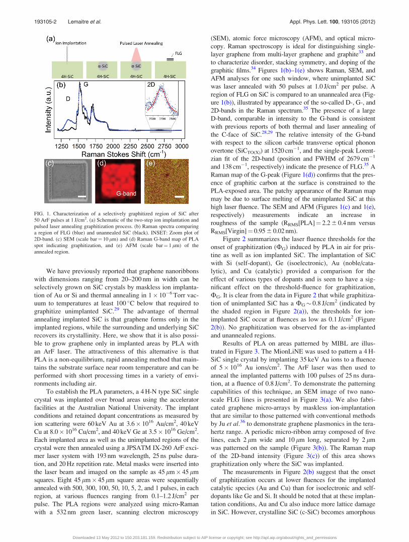
graphitic films.34 Figures 1(b)–1(e) shows Raman, SEM, and
AFM analyses for one such window, where unimplanted SiC
was laser annealed with 50 pulses at 1.0 J/cm2 per pulse. A
region of FLG on SiC is compared to an unannealed area (Fig-
ure 1(b)), illustrated by appearance of the so-called D-, G-, and
2D-bands in the Raman spectrum.35 The presence of a large
D-band, comparable in intensity to the G-band is consistent
with previous reports of both thermal and laser annealing of
the C-face of SiC.28,29 The relative intensity of the G-band
with respect to the silicon carbide transverse optical phonon
overtone (SiCTO(X)) at 1520 cm�1, and the single-peak Lorent-
zian fit of the 2D-band (position and FWHM of 2679 cm�1
and 138 cm�1, respectively) indicate the presence of FLG.35 A
Raman map of the G-peak (Figure 1(d)) confirms that the pres-
ence of graphitic carbon at the surface is constrained to the
PLA-exposed area. The patchy appearance of the Raman map
may be due to surface melting of the unimplanted SiC at this
high laser fluence. The SEM and AFM (Figures 1(c) and 1(e),
respectively) measurements indicate an increase in
roughness of the sample (RRMS[PLA]¼ 2.2 6 0.4 nm versus
RRMS[Virgin]¼ 0.95 6 0.02 nm).
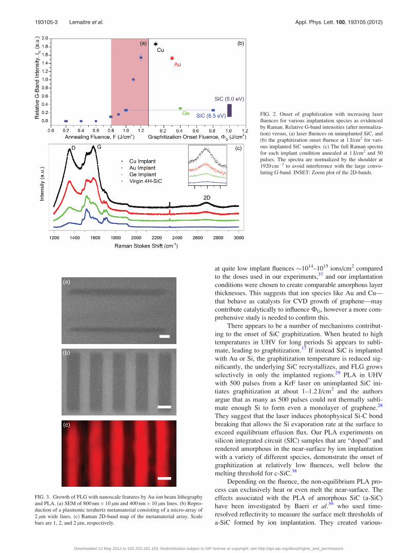
Figure 2 summarizes the laser fluence thresholds for the
onset of graphitization (AG) induced by PLA in air for pris-
tine as well as ion implanted SiC. The implantation of SiC
with Si (self-dopant), Ge (isoelectronic), Au (noble/cata-
lytic), and Cu (catalytic) provided a comparison for the
effect of various types of dopants and is seen to have a sig-
nificant effect on the threshold-fluence for graphitization,
AG. It is clear from the data in Figure 2 that while graphitiza-
tion of unimplanted SiC has a AG� 0.8 J/cm2 (indicated by
the shaded region in Figure 2(a)), the thresholds for ion-
implanted SiC occur at fluences as low as 0.1 J/cm2 (Figure
2(b)). No graphitization was observed for the as-implanted
and unannealed regions.
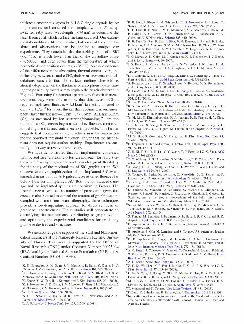
Results of PLA on areas patterned by MIBL are illus-
trated in Figure 3. The MionLiNE was used to pattern a 4 H-
SiC single crystal by implanting 35 keV Au ions to a fluence
of 5� 1016 Au ions/cm2. The ArF laser was then used to
anneal the implanted patterns with 100 pulses of 25 ns dura-
tion, at a fluence of 0.8 J/cm2. To demonstrate the patterning
capabilities of this technique, an SEM image of two nano-
scale FLG lines is presented in Figure 3(a). We also fabri-
cated graphene micro-arrays by maskless ion-implantation
that are similar to those patterned with conventional methods
by Ju et al.36 to demonstrate graphene plasmonics in the tera-
hertz range. A periodic micro-ribbon array composed of five
lines, each 2 lm wide and 10 lm long, separated by 2 lm
was patterned on the sample (Figure 3(b)). The Raman map
of the 2D-band intensity (Figure 3(c)) of this area shows
graphitization only where the SiC was implanted.
The measurements in Figure 2(b) suggest that the onset
of graphitization occurs at lower fluences for the implanted
catalytic species (Au and Cu) than for isoelectronic and self-
dopants like Ge and Si. It should be noted that at these implan-
tation conditions, Au and Cu also induce more lattice damage
in SiC. However, crystalline SiC (c-SiC) becomes amorphous
FIG. 1. Characterization of a selectively graphitized region of SiC after
50 ArF pulses at 1 J/cm2. (a) Schematic of the two-step ion implantation and
pulsed laser annealing graphitization process. (b) Raman spectra comparing
a region of FLG (blue) and unannealed SiC (black). INSET: Zoom plot of
2D-band. (c) SEM (scale bar¼ 10 lm) and (d) Raman G-band map of PLA
spot indicating graphitization, and (e) AFM (scale bar¼ 1 lm) of the
annealed region.
193105-2 Lemaitre et al. Appl. Phys. Lett. 100, 193105 (2012)
Downloaded 13 May 2012 to 150.203.181.159. Redistribution subject to AIP license or copyright; see http://apl.aip.org/about/rights_and_permissions
at quite low implant fluences �1014–1015 ions/cm2 compared
to the doses used in our experiments,37 and our implantation
conditions were chosen to create comparable amorphous layer
thicknesses. This suggests that ion species like Au and Cu—
that behave as catalysts for CVD growth of graphene—may
contribute catalytically to influence AG, however a more com-
prehensive study is needed to confirm this.
There appears to be a number of mechanisms contribut-
ing to the onset of SiC graphitization. When heated to high
temperatures in UHV for long periods Si appears to subli-
mate, leading to graphitization.17 If instead SiC is implanted
with Au or Si, the graphitization temperature is reduced sig-
nificantly, the underlying SiC recrystallizes, and FLG grows
selectively in only the implanted regions.29 PLA in UHV
with 500 pulses from a KrF laser on unimplanted SiC ini-
tiates graphitization at about 1–1.2 J/cm2 and the authors
argue that as many as 500 pulses could not thermally subli-
mate enough Si to form even a monolayer of graphene.28
They suggest that the laser induces photophysical Si-C bond
breaking that allows the Si evaporation rate at the surface to
exceed equilibrium effusion flux. Our PLA experiments on
silicon integrated circuit (SIC) samples that are “doped” and
rendered amorphous in the near-surface by ion implantation
with a variety of different species, demonstrate the onset of
graphitization at relatively low fluences, well below the
melting threshold for c-SiC.38
Depending on the fluence, the non-equilibrium PLA pro-
cess can exclusively heat or even melt the near-surface. The
effects associated with the PLA of amorphous SiC (a-SiC)
have been investigated by Baeri et al.39 who used time-
resolved reflectivity to measure the surface melt thresholds of
a-SiC formed by ion implantation. They created various-
FIG. 3. Growth of FLG with nanoscale features by Au-ion beam lithography
and PLA. (a) SEM of 800 nm� 10 lm and 400 nm� 10 lm lines. (b) Repro-
duction of a plasmonic terahertz metamaterial consisting of a micro-array of
2 lm wide lines. (c) Raman 2D-band map of the metamaterial array. Scale
bars are 1, 2, and 2 lm, respectively.
FIG. 2. Onset of graphitization with increasing laser
fluences for various implantation species as evidenced
by Raman. Relative G-band intensities (after normaliza-
tion) versus, (a) laser fluences on unimplanted SiC, and
(b) the graphitization onset fluence at 1 J/cm2 for vari-
ous implanted SiC samples. (c) The full Raman spectra
for each implant condition annealed at 1 J/cm2 and 50
pulses. The spectra are normalized by the shoulder at
1920 cm�2 to avoid interference with the large convo-
luting G-band. INSET: Zoom plot of the 2D-bands.
193105-3 Lemaitre et al. Appl. Phys. Lett. 100, 193105 (2012)
Downloaded 13 May 2012 to 150.203.181.159. Redistribution subject to AIP license or copyright; see http://apl.aip.org/about/rights_and_permissions
thickness amorphous layers in 6 H-SiC single crystals by Ar
implantations and annealed the samples with a 25 ns, q-
switched ruby laser (wavelength¼ 694 nm) to determine the
laser fluences at which surface melting occurred. Our experi-
mental conditions differ somewhat, but some of their conclu-
sions and observations can be applied to analyze our
experiments. They concluded that the melting point of a-SiC
(�2445 K) is much lower than that of the crystalline phase
(�3500 K), and even lower than the temperature at which
peritectic decomposition occurs (�2850 K). As a consequence
of the differences in the absorption, thermal conductivity, and
diffusivity between a- and c-SiC, their measurements and cal-
culations conclude that the surface melting threshold is
strongly dependent on the thickness of amorphous layers, rais-
ing the possibility that this may explain the trends observed in
Figure 2. Extracting fundamental parameters from their meas-
urements, they were able to show that thin layers �50 nm
required high laser fluences �1.3 J/cm2 to melt, compared to
only �0.4 J/cm2 for layers thicker than 200 nm. But our amor-
phous layer thicknesses—33 nm (Cu), 26 nm (Au), and 31 nm
(Ge), as measured by ion scattering/channeling40—are too
thin and our AG onsets begin at such low fluences compared
to melting that this mechanism seems improbable. This further
suggests that doping or catalytic effects may be responsible
for the observed threshold reduction, and/or that the mecha-
nism does not require surface melting. Experiments are cur-
rently underway to resolve these issues.
We have demonstrated that ion implantation combined
with pulsed laser annealing offers an approach for rapid syn-
thesis of few-layer graphene and provides great flexibility
for the study of the mechanisms of SiC graphitization. We
observe selective graphitization of ion implanted SiC when
annealed in air with an ArF pulsed laser at onset fluences far
below those for unimplanted SiC. Both the ion induced dam-
age and the implanted species are contributing factors. The
laser fluence as well as the number of pulses at a given flu-
ence can also be used to control the amount of graphitization.
Coupled with multi-ion beam lithography, these techniques
provide a low-temperature approach for direct synthesis of
graphene nanostructures. Future studies will concentrate on
quantifying the mechanisms contributing to graphitization
and optimizing the experimental conditions for producing
graphene devices and structures.
We acknowledge the support of the Staff and Nanofabri-
cation Engineers at the Nanoscale Research Facility, Univer-
sity of Florida. This work is supported by the Office of
Naval Research (ONR) under Contract Number 00075094
(BRA) and by the National Science Foundation (NSF) under
Contract Number 1005301 (AFH).
1K. S. Novoselov, A. K. Geim, S. V. Morozov, D. Jiang, Y. Zhang, S. V.
Dubonos, I. V. Grigorieva, and A. A. Firsov, Science 306, 666 (2004).2K. S. Novoselov, D. Jiang, F. Schedin, T. J. Booth, V. V. Khotkevich, S. V.
Morozov, and A. K. Geim, Proc. Natl. Acad. Sci. U.S.A. 102, 10451 (2005).3Y. Zhang, Y.-W. Tan, H. L. Stormer, and P. Kim, Nature 438, 201 (2005).4K. S. Novoselov, A. K. Geim, S. V. Morozov, D. Jiang, M. I. Katsnelson, I.
V. Grigorieva, S. V. Dubonos, and A. A. Firsov, Nature 438, 197 (2005).5A. K. Geim, Science 324, 1530 (2009).6A. H. C. Neto, F. Guinea, N. M. R. Peres, K. S. Novoselov, and A. K.
Geim, Rev. Mod. Phys. 81, 109 (2009).7L. A. Falkovsky, J. Phys.: Conf. Ser. 129, 012004 (2008).
8R. R. Nair, P. Blake, A. N. Grigorenko, K. S. Novoselov, T. J. Booth, T.
Stauber, N. M. R. Peres, and A. K. Geim, Science 320, 1308 (2008).9D. C. Elias, R. R. Nair, T. M. G. Mohiuddin, S. V. Morozov, P. Blake, M.
P. Halsall, A. C. Ferrari, D. W. Boukhvalov, M. I. Katsnelson, A. K.
Geim, and K. S. Novoselov, Science 323, 610 (2009).10R. R. Nair, W. Ren, R. Jalil, I. Riaz, V. G. Kravets, L. Britnell, P. Blake,
F. Schedin, A. S. Mayorov, S. Yuan, M. I. Katsnelson, H. Cheng, W. Stru-
pinski, L. G. Bulusheva, A. V. Okotrub, I. V. Grigorieva, A. N. Grigor-
enko, K. S. Novoselov, and A. K. Geim, Small 6, 2877 (2010).11J. C. Meyer, A. K. Geim, M. I. Katsnelson, K. S. Novoselov, T. J. Booth,
and S. Roth, Nature 446, 60 (2007).12J. S. Bunch, A. M. Van Der Zande, S. S. Verbridge, I. W. Frank, D. M.
Tanenbaum, J. M. Parpia, H. G. Craighead, and P. L. McEuen, Science
315, 490 (2007).13K. I. Bolotin, K. J. Sikes, Z. Jiang, M. Klima, G. Fudenberg, J. Hone, P.
Kim, and H. L. Stormer, Solid State Commun. 146, 351 (2008).14A. Reina, X. Jia, J. Ho, D. Nezich, H. Son, V. Bulovic, M. S. Dresselhaus,
and J. Kong, Nano Lett. 9, 30 (2008).15X. Li, W. Cai, J. An, S. Kim, J. Nah, D. Yang, R. Piner, A. Velamakanni,
I. Jung, E. Tutuc, S. K. Banerjee, L. Colombo, and R. S. Ruoff, Science
324, 1312 (2009).16S. Lee, K. Lee, and Z. Zhong, Nano Lett. 10, 4702 (2010).17K. V. Emtsev, A. Bostwick, K. Horn, J. Jobst, G. L. Kellogg, L. Ley, J. L.
McChesney, T. Ohta, S. A. Reshanov, J. Rohrl, E. Rotenberg, A. K. Schmid,
D. Waldmann, H. B. Weber, and T. Seyller, Nature Mater. 8, 203 (2009).18Y.-M. Lin, C. Dimitrakopoulos, K. A. Jenkins, D. B. Farmer, H.-Y. Chiu,
A. Grill, and P. Avouris, Science 327, 662 (2010).19J. Robinson, X. Weng, K. Trumbull, R. Cavalero, M. Wetherington, E.
Frantz, M. LaBella, Z. Hughes, M. Fanton, and D. Snyder, ACS Nano 4,
153 (2009).20M. Y. Han, B. Ozyilmaz, Y. Zhang, and P. Kim, Phys. Rev. Lett. 98,
206805 (2007).21B. Ozyilmaz, P. Jarillo-Herrero, D. Efetov, and P. Kim, Appl. Phys. Lett.
91, 192107 (2007).22Z. H. Ni, T. Yu, Y. H. Lu, Y. Y. Wang, Y. P. Feng, and Z. X. Shen, ACS
Nano 2, 2301 (2008).23T. O. Wehling, K. S. Novoselov, S. V. Morozov, E. E. Vdovin, M. I. Kats-
nelson, A. K. Geim, and A. I. Lichtenstein, Nano Lett. 8, 173 (2007).24X. Wang, X. Li, L. Zhang, Y. Yoon, P. K. Weber, H. Wang, J. Guo, and
H. Dai, Science 324, 768 (2009).25S. Tongay, K. Berke, M. Lemaitre, Z. Nasrollahi, D. B. Tanner, A. F.
Hebard, and B. R. Appleton, Nanotechnology 22, 425701 (2011).26Y. Zhang, T.-T. Tang, C. Girit, Z. Hao, M. C. Martin, A. Zettl, M. F.
Crommie, Y. R. Shen, and F. Wang, Nature 459, 820 (2009).27D. Perrone, G. Maccioni, A. Chiolerio, C. Martinez de Marigorta, M.
Naretto, P. Pandolfi, P. Martino, C. Ricciardi, A. Chiodoni, E. Celasco, L.
Scaltrito, and S. Ferrero, in Proceedings of the Fifth International
WLT-Conference on Laser Manufacturing, Munich, June 2009.28S. Lee, M. F. Toney, W. Ko, J. C. Randel, H. J. Jung, K. Munakata, J. Lu,
T. H. Geballe, M. R. Beasley, R. Sinclair, H. C. Manoharan, and A. Salleo,
ACS Nano 4, 7524 (2010).29S. Tongay, M. Lemaitre, J. Fridmann, A. F. Hebard, B. P. Gila, and B. R.
Appleton, Appl. Phys. Lett. 100, 073501 (2012).30B. Appleton and B. Gila, U.S. patent application pct/us2010/024723
(2 February 2009).31B. Appleton, B. Gila, M. Lemaitre, and S. Tongay, U.S. patent application
61/526,510 (8 August 2011).32B. R. Appleton, S. Tongay, M. Lemaitre, B. Gila, J. Fridmann, P.
Mazarov, J. E. Sanabia, S. Bauerdick, L. Bruchhaus, R. Mimura, and R.
Jede, Nucl. Instrum. Methods Phys. Res. B 272, 153 (2012).33A. C. Ferrari, J. C. Meyer, V. Scardaci, C. Casiraghi, M. Lazzeri, F. Mauri,
S. Piscanec, D. Jiang, K. S. Novoselov, S. Roth, and A. K. Geim, Phys.
Rev. Lett. 97, 187401 (2006).34A. C. Ferrari, Solid State Commun. 143, 47 (2007).35Z. H. Ni, W. Chen, X. F. Fan, J. L. Kuo, T. Yu, A. T. S. Wee, and Z. X.
Shen, Phys. Rev. B 77, 115416 (2008).36L. Ju, B. Geng, J. Horng, C. Girit, M. Martin, Z. Hao, H. A. Bechtel, X.
Liang, A. Zettl, Y. R. Shen, and F. Wang, Nat. Nanotechnol. 6, 630 (2011).37M. V. Rao, P. Griffiths, O. W. Holland, G. Kelner, J. A. Freitas, D. S.
Simons, P. H. Chi, and M. Ghezzo, J. Appl. Phys. 77, 2479 (1995).38T. Mizunami and N. Toyama, Opt. Laser Technol. 35, 451 (2003).39P. Baeri, C. Spinella, and R. Reitano, Int. J. Thermophys. 20, 1211 (1999).40Ion scattering/channeling measurements made at the Vanderbilt University
accelerator facility in collaboration with Leonard Feldman, Sarit Dhar, and
Anthony Hmelo.
193105-4 Lemaitre et al. Appl. Phys. Lett. 100, 193105 (2012)
Downloaded 13 May 2012 to 150.203.181.159. Redistribution subject to AIP license or copyright; see http://apl.aip.org/about/rights_and_permissions