Embed Size (px)
Citation preview
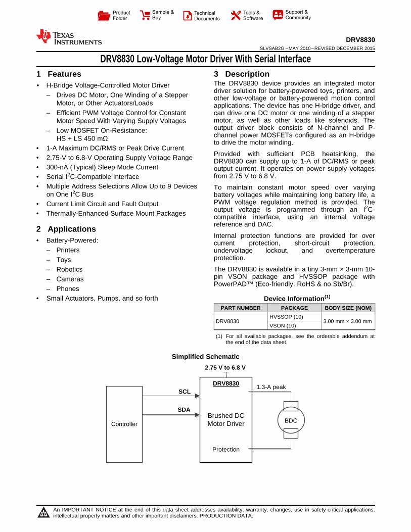
2.75 V to 6.8 V
DRV8830
Brushed DC Motor Driver BDC
SCL1.3-A peak
Controller
Protection
SDA
Product
Folder
Sample &Buy
Technical
Documents
Tools &
Software
Support &Community
DRV8830SLVSAB2G –MAY 2010–REVISED DECEMBER 2015
DRV8830 Low-Voltage Motor Driver With Serial Interface1 Features 3 Description
The DRV8830 device provides an integrated motor1• H-Bridge Voltage-Controlled Motor Driver
driver solution for battery-powered toys, printers, and– Drives DC Motor, One Winding of a Stepper other low-voltage or battery-powered motion controlMotor, or Other Actuators/Loads applications. The device has one H-bridge driver, and
– Efficient PWM Voltage Control for Constant can drive one DC motor or one winding of a steppermotor, as well as other loads like solenoids. TheMotor Speed With Varying Supply Voltagesoutput driver block consists of N-channel and P-– Low MOSFET On-Resistance:channel power MOSFETs configured as an H-bridgeHS + LS 450 mΩ to drive the motor winding.
• 1-A Maximum DC/RMS or Peak Drive CurrentProvided with sufficient PCB heatsinking, the• 2.75-V to 6.8-V Operating Supply Voltage Range DRV8830 can supply up to 1-A of DC/RMS or peak
• 300-nA (Typical) Sleep Mode Current output current. It operates on power supply voltagesfrom 2.75 V to 6.8 V.• Serial I2C-Compatible Interface
• Multiple Address Selections Allow Up to 9 Devices To maintain constant motor speed over varyingon One I2C Bus battery voltages while maintaining long battery life, a
PWM voltage regulation method is provided. The• Current Limit Circuit and Fault Outputoutput voltage is programmed through an I2C-• Thermally-Enhanced Surface Mount Packages compatible interface, using an internal voltagereference and DAC.2 ApplicationsInternal protection functions are provided for over
• Battery-Powered: current protection, short-circuit protection,– Printers undervoltage lockout, and overtemperature
protection.– ToysThe DRV8830 is available in a tiny 3-mm × 3-mm 10-– Roboticspin VSON package and HVSSOP package with– CamerasPowerPAD™ (Eco-friendly: RoHS & no Sb/Br).
– Phones• Small Actuators, Pumps, and so forth Device Information(1)
PART NUMBER PACKAGE BODY SIZE (NOM)HVSSOP (10)
DRV8830 3.00 mm × 3.00 mmVSON (10)
(1) For all available packages, see the orderable addendum atthe end of the data sheet.
Simplified Schematic
1
An IMPORTANT NOTICE at the end of this data sheet addresses availability, warranty, changes, use in safety-critical applications,intellectual property matters and other important disclaimers. PRODUCTION DATA.
DRV8830SLVSAB2G –MAY 2010–REVISED DECEMBER 2015 www.ti.com
Table of Contents7.6 Register Maps ......................................................... 131 Features .................................................................. 1
8 Application and Implementation ........................ 152 Applications ........................................................... 18.1 Application Information............................................ 153 Description ............................................................. 18.2 Typical Application ................................................. 154 Revision History..................................................... 2
9 Power Supply Recommendations ...................... 195 Pin Configuration and Functions ......................... 39.1 Power Supervisor.................................................... 196 Specifications......................................................... 39.2 Bulk Capacitance .................................................... 196.1 Absolute Maximum Ratings ...................................... 3
10 Layout................................................................... 206.2 ESD Ratings.............................................................. 410.1 Layout Guidelines ................................................. 206.3 Recommended Operating Conditions....................... 410.2 Layout Example .................................................... 206.4 Thermal Information .................................................. 410.3 Thermal Considerations ........................................ 206.5 Electrical Characteristics........................................... 5
11 Device and Documentation Support ................. 216.6 I2C Timing Requirements.......................................... 611.1 Documentation Support ........................................ 216.7 Typical Characteristics .............................................. 711.2 Community Resources.......................................... 217 Detailed Description .............................................. 811.3 Trademarks ........................................................... 217.1 Overview ................................................................... 811.4 Electrostatic Discharge Caution............................ 217.2 Functional Block Diagram ......................................... 811.5 Glossary ................................................................ 217.3 Feature Description................................................... 8
12 Mechanical, Packaging, and Orderable7.4 Device Functional Modes........................................ 11Information ........................................................... 217.5 Programming........................................................... 12
4 Revision HistoryNOTE: Page numbers for previous revisions may differ from page numbers in the current version.
Changes from Revision F (February 2012) to Revision G Page
• Added Pin Configuration and Functions section, ESD Ratings table, Feature Description section, Device FunctionalModes, Application and Implementation section, Power Supply Recommendations section, Layout section, Deviceand Documentation Support section, and Mechanical, Packaging, and Orderable Information section .............................. 1
2 Submit Documentation Feedback Copyright © 2010–2015, Texas Instruments Incorporated
Product Folder Links: DRV8830
1
2
3
4
10
9
8
7
GND
(ThermalPad)
SCL
SDA
A1
A0
OUT1
VCC
ISENSE
OUT2
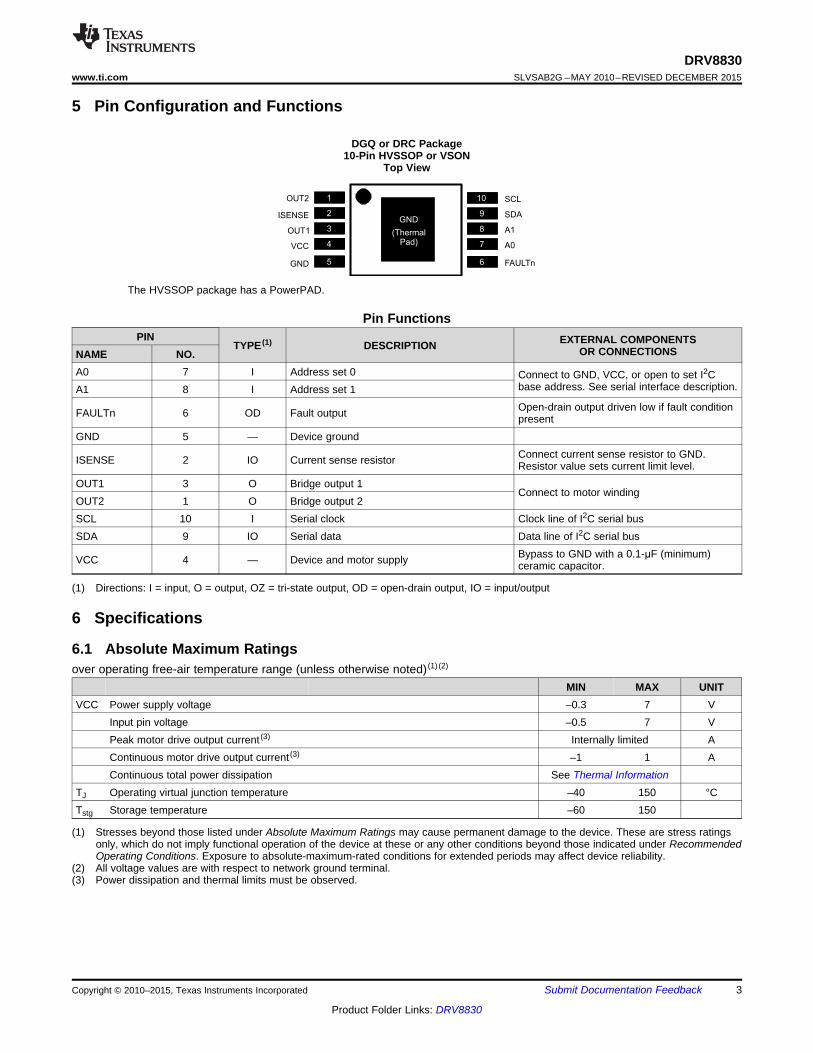
5 6 FAULTnGND
DRV8830www.ti.com SLVSAB2G –MAY 2010–REVISED DECEMBER 2015
5 Pin Configuration and Functions
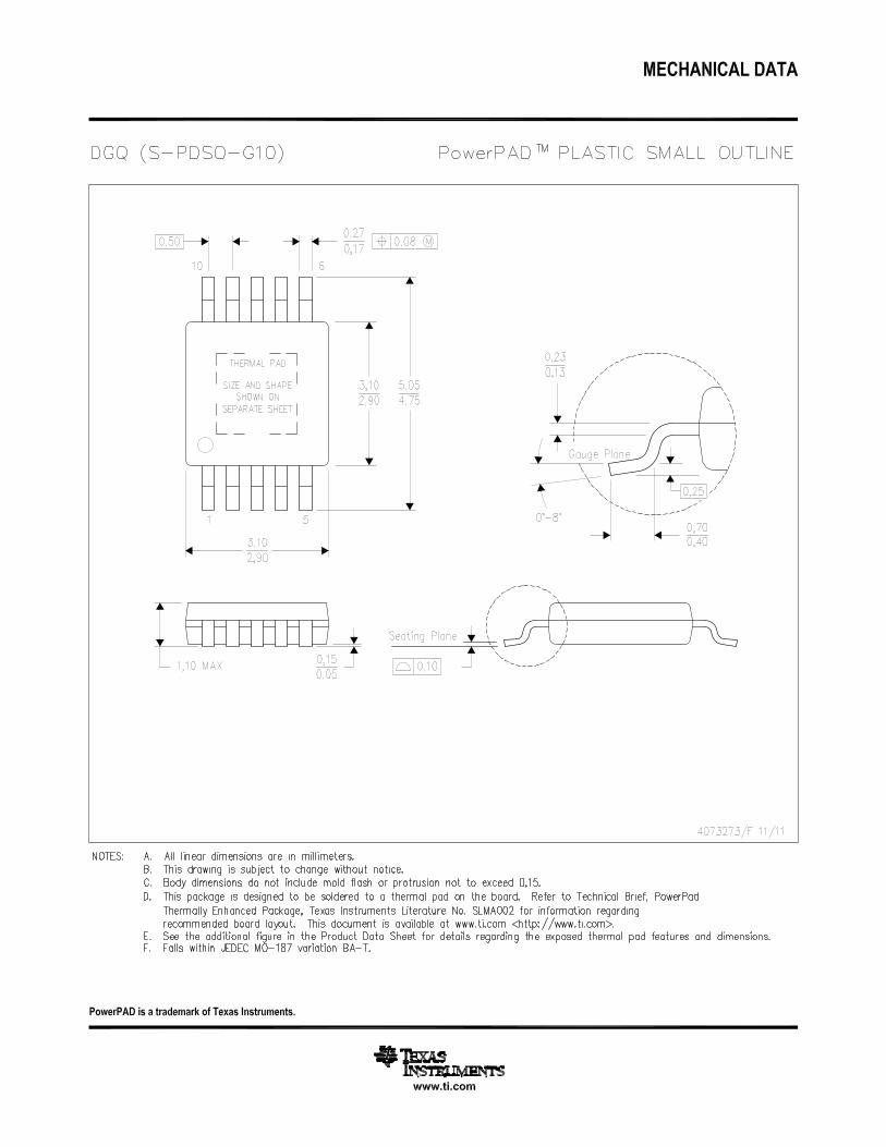
DGQ or DRC Package10-Pin HVSSOP or VSON
Top View
The HVSSOP package has a PowerPAD.
Pin FunctionsPIN EXTERNAL COMPONENTSTYPE (1) DESCRIPTION OR CONNECTIONSNAME NO.
A0 7 I Address set 0 Connect to GND, VCC, or open to set I2Cbase address. See serial interface description.A1 8 I Address set 1Open-drain output driven low if fault conditionFAULTn 6 OD Fault output present
GND 5 — Device groundConnect current sense resistor to GND.ISENSE 2 IO Current sense resistor Resistor value sets current limit level.
OUT1 3 O Bridge output 1Connect to motor winding
OUT2 1 O Bridge output 2SCL 10 I Serial clock Clock line of I2C serial busSDA 9 IO Serial data Data line of I2C serial bus
Bypass to GND with a 0.1-μF (minimum)VCC 4 — Device and motor supply ceramic capacitor.
(1) Directions: I = input, O = output, OZ = tri-state output, OD = open-drain output, IO = input/output
6 Specifications
6.1 Absolute Maximum Ratingsover operating free-air temperature range (unless otherwise noted) (1) (2)
MIN MAX UNITVCC Power supply voltage –0.3 7 V
Input pin voltage –0.5 7 VPeak motor drive output current (3) Internally limited AContinuous motor drive output current (3) –1 1 AContinuous total power dissipation See Thermal Information
TJ Operating virtual junction temperature –40 150 °CTstg Storage temperature –60 150
(1) Stresses beyond those listed under Absolute Maximum Ratings may cause permanent damage to the device. These are stress ratingsonly, which do not imply functional operation of the device at these or any other conditions beyond those indicated under RecommendedOperating Conditions. Exposure to absolute-maximum-rated conditions for extended periods may affect device reliability.
(2) All voltage values are with respect to network ground terminal.(3) Power dissipation and thermal limits must be observed.
Copyright © 2010–2015, Texas Instruments Incorporated Submit Documentation Feedback 3
Product Folder Links: DRV8830
DRV8830SLVSAB2G –MAY 2010–REVISED DECEMBER 2015 www.ti.com
6.2 ESD RatingsVALUE UNIT
Human body model (HBM), per ANSI/ESDA/JEDEC JS-001 (1) ±2000ElectrostaticV(ESD) Vdischarge Charged-device model (CDM), per JEDEC specification JESD22-C101 (2) ±1000
(1) JEDEC document JEP155 states that 500-V HBM allows safe manufacturing with a standard ESD control process.(2) JEDEC document JEP157 states that 250-V CDM allows safe manufacturing with a standard ESD control process.
6.3 Recommended Operating Conditionsover operating free-air temperature range (unless otherwise noted)
MIN MAX UNITVCC Motor power supply voltage 2.75 6.8 VIOUT Continuous or peak H-bridge output current (1) 0 1 A
(1) Power dissipation and thermal limits must be observed.
6.4 Thermal InformationDRV8830
THERMAL METRIC (1) DGQ (HVSSOP) DRC (VSON) UNIT10 PINS 10 PINS
RθJA Junction-to-ambient thermal resistance 69.3 50.2 °C/WRθJC(top) Junction-to-case (top) thermal resistance 63.5 78.4 °C/WRθJB Junction-to-board thermal resistance 51.6 18.8 °C/WψJT Junction-to-top characterization parameter 1.5 1.1 °C/WψJB Junction-to-board characterization parameter 23.2 17.9 °C/WRθJB Junction-to-case (bottom) thermal resistance 9.5 5.1 °C/W
(1) For more information about traditional and new thermal metrics, see the Semiconductor and IC Package Thermal Metrics applicationreport, SPRA953.
4 Submit Documentation Feedback Copyright © 2010–2015, Texas Instruments Incorporated
Product Folder Links: DRV8830
DRV8830www.ti.com SLVSAB2G –MAY 2010–REVISED DECEMBER 2015
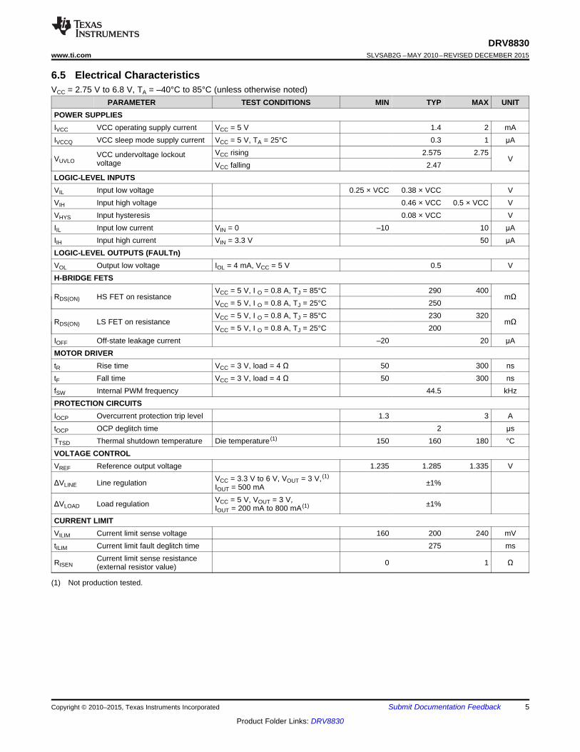
6.5 Electrical CharacteristicsVCC = 2.75 V to 6.8 V, TA = –40°C to 85°C (unless otherwise noted)
PARAMETER TEST CONDITIONS MIN TYP MAX UNITPOWER SUPPLIESIVCC VCC operating supply current VCC = 5 V 1.4 2 mAIVCCQ VCC sleep mode supply current VCC = 5 V, TA = 25°C 0.3 1 μA
VCC rising 2.575 2.75VCC undervoltage lockoutVUVLO Vvoltage VCC falling 2.47LOGIC-LEVEL INPUTSVIL Input low voltage 0.25 × VCC 0.38 × VCC VVIH Input high voltage 0.46 × VCC 0.5 × VCC VVHYS Input hysteresis 0.08 × VCC VIIL Input low current VIN = 0 –10 10 μAIIH Input high current VIN = 3.3 V 50 μALOGIC-LEVEL OUTPUTS (FAULTn)VOL Output low voltage IOL = 4 mA, VCC = 5 V 0.5 VH-BRIDGE FETS
VCC = 5 V, I O = 0.8 A, TJ = 85°C 290 400RDS(ON) HS FET on resistance mΩ
VCC = 5 V, I O = 0.8 A, TJ = 25°C 250VCC = 5 V, I O = 0.8 A, TJ = 85°C 230 320
RDS(ON) LS FET on resistance mΩVCC = 5 V, I O = 0.8 A, TJ = 25°C 200
IOFF Off-state leakage current –20 20 μAMOTOR DRIVERtR Rise time VCC = 3 V, load = 4 Ω 50 300 nstF Fall time VCC = 3 V, load = 4 Ω 50 300 nsfSW Internal PWM frequency 44.5 kHzPROTECTION CIRCUITSIOCP Overcurrent protection trip level 1.3 3 AtOCP OCP deglitch time 2 μsTTSD Thermal shutdown temperature Die temperature (1) 150 160 180 °CVOLTAGE CONTROLVREF Reference output voltage 1.235 1.285 1.335 V
VCC = 3.3 V to 6 V, VOUT = 3 V, (1)ΔVLINE Line regulation ±1%IOUT = 500 mA
VCC = 5 V, VOUT = 3 V,ΔVLOAD Load regulation ±1%IOUT = 200 mA to 800 mA (1)
CURRENT LIMITVILIM Current limit sense voltage 160 200 240 mVtILIM Current limit fault deglitch time 275 ms
Current limit sense resistanceRISEN 0 1 Ω(external resistor value)
(1) Not production tested.
Copyright © 2010–2015, Texas Instruments Incorporated Submit Documentation Feedback 5
Product Folder Links: DRV8830
SCL
SDA0.7 VCC
0.3 VCC
0.7 VCC
0.3 VCC9
D7/A
tvd
tsds
tsps
tbuf
Stop Condition
Start Condition
8
SCL
SDA0.7 VCC
0.3 VCC
0.7 VCC
0.3 VCC
1/fscl
tscl
tsch
ticf
ticf
ticr tsdh
tsdsticr
tvd
tsth
Start Condition
1 2 3 4
DRV8830SLVSAB2G –MAY 2010–REVISED DECEMBER 2015 www.ti.com
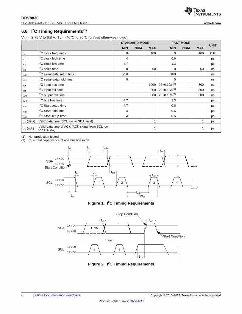
6.6 I2C Timing Requirements (1)
VCC = 2.75 V to 6.8 V, TA = -40°C to 85°C (unless otherwise noted)STANDARD MODE FAST MODE
UNITMIN NOM MAX MIN NOM MAX
fscl I2C clock frequency 0 100 0 400 kHztsch I2C clock high time 4 0.6 µstscl I2C clock low time 4.7 1.3 µstsp I2C spike time 0 50 0 50 nstsds I2C serial data setup time 250 100 nstsdh I2C serial data hold time 0 0 nsticr I2C input rise time 1000 20+0.1Cb (2) 300 nsticf I2C input fall time 300 20+0.1Cb (2) 300 nstocf I2C output fall time 300 20+0.1Cb (2) 300 nstbuf I2C bus free time 4.7 1.3 µststs I2C Start setup time 4.7 0.6 µststh I2C Start hold time 4 0.6 µstsps I2C Stop setup time 4 0.6 µstvd (data) Valid data time (SCL low to SDA valid) 1 1 µs
Valid data time of ACK (ACK signal from SCL lowtvd (ack) 1 1 µsto SDA low)
(1) Not production tested.(2) Cb = total capacitance of one bus line in pF
Figure 1. I2C Timing Requirements
Figure 2. I2C Timing Requirements
6 Submit Documentation Feedback Copyright © 2010–2015, Texas Instruments Incorporated
Product Folder Links: DRV8830
VCC(V)
RD
S(O
N)(
HS
+LS
) (m:
)
2.75 3.25 3.75 4.25 4.75 5.25 5.75 6350375400425450475500525550575600625650675700725
D003
-40qC25qC85qC
VCC(V)
I VC
C(u
A)
2.75 3.25 3.75 4.25 4.75 5.25 5.75 61000
1200
1400
1600
1800
2000
D001
-40qC25qC85qC
VCC(V)
I VC
CQ
(nA
)
2.75 3.25 3.75 4.25 4.75 5.25 5.75 650
100
150
200
250
300
350
400
450
500
550
D002
-40qC25qC85qC
50%
55%
60%
65%
70%
75%
80%
85%
90%
95%
100%
0.2 0.4 0.6 0.8
LOAD - A
EF
FIC
IEN
CY
0%
10%
20%
30%
40%
50%
60%
70%
80%
90%
100%
0.5 1.5 2.5 3.5 4.5 5.5
V - VOUT
EF
FIC
EN
CY
Linear Regulator
DRV8830
DRV8830www.ti.com SLVSAB2G –MAY 2010–REVISED DECEMBER 2015
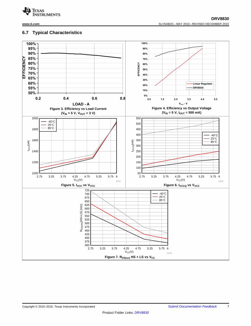
6.7 Typical Characteristics
Figure 4. Efficiency vs Output VoltageFigure 3. Efficiency vs Load Current(VIN = 5 V, IOUT = 500 mA)(VIN = 5 V, VOUT = 3 V)
Figure 5. IVCC vs VVCC Figure 6. IVCCQ vs VVCC
Figure 7. RDS(on) HS + LS vs VCC
Copyright © 2010–2015, Texas Instruments Incorporated Submit Documentation Feedback 7
Product Folder Links: DRV8830
Over-
Temp
OUT1
OUT2
GND
SDA
A0
A1
VCC
VCC
VCC
Battery
DCM
Gate
Drive
Integ.
Comp
+
-
Ref
Osc
OCP
VCC
Gate
Drive
OCP
SCL
Current
Sense
FAULTn
ISENSE
I2C
Addr
Sel
5
Logic
DAC
DRV8830SLVSAB2G –MAY 2010–REVISED DECEMBER 2015 www.ti.com
7 Detailed Description
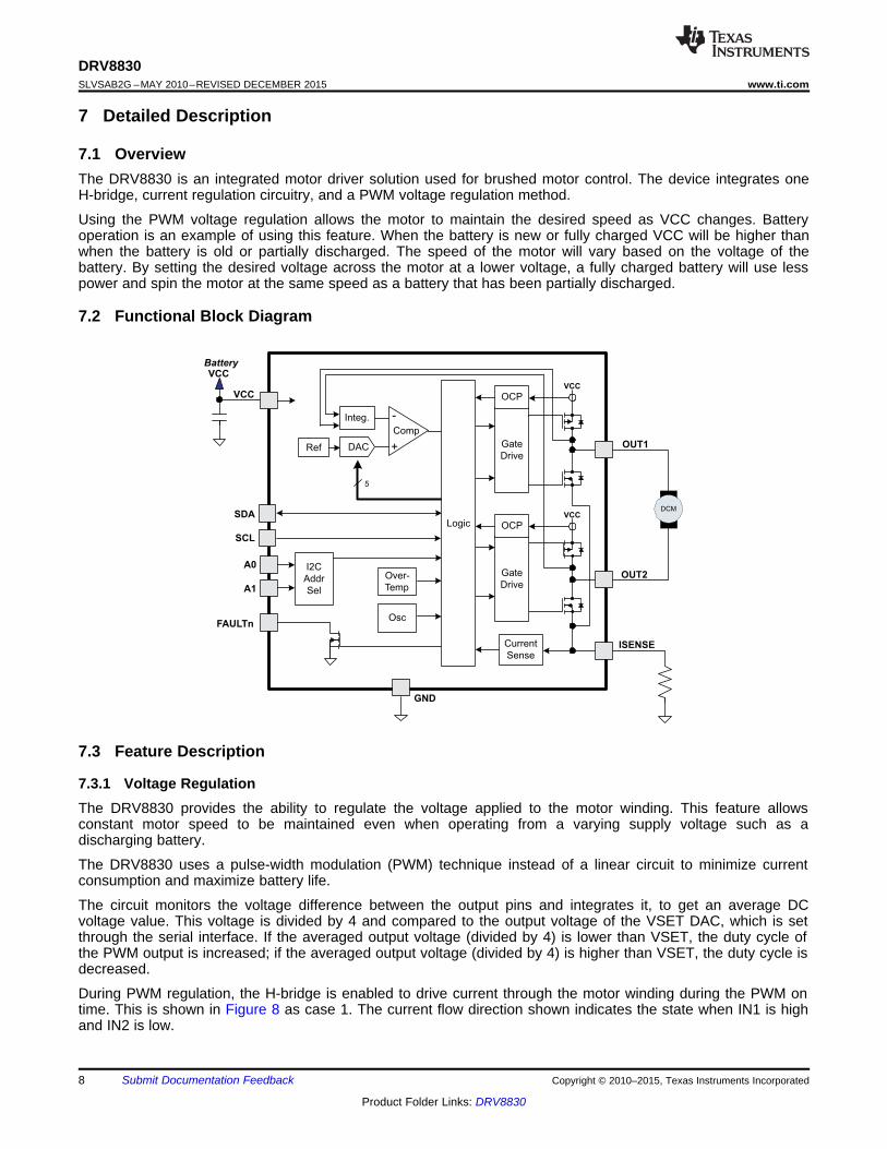
7.1 OverviewThe DRV8830 is an integrated motor driver solution used for brushed motor control. The device integrates oneH-bridge, current regulation circuitry, and a PWM voltage regulation method.
Using the PWM voltage regulation allows the motor to maintain the desired speed as VCC changes. Batteryoperation is an example of using this feature. When the battery is new or fully charged VCC will be higher thanwhen the battery is old or partially discharged. The speed of the motor will vary based on the voltage of thebattery. By setting the desired voltage across the motor at a lower voltage, a fully charged battery will use lesspower and spin the motor at the same speed as a battery that has been partially discharged.
7.2 Functional Block Diagram
7.3 Feature Description
7.3.1 Voltage RegulationThe DRV8830 provides the ability to regulate the voltage applied to the motor winding. This feature allowsconstant motor speed to be maintained even when operating from a varying supply voltage such as adischarging battery.
The DRV8830 uses a pulse-width modulation (PWM) technique instead of a linear circuit to minimize currentconsumption and maximize battery life.
The circuit monitors the voltage difference between the output pins and integrates it, to get an average DCvoltage value. This voltage is divided by 4 and compared to the output voltage of the VSET DAC, which is setthrough the serial interface. If the averaged output voltage (divided by 4) is lower than VSET, the duty cycle ofthe PWM output is increased; if the averaged output voltage (divided by 4) is higher than VSET, the duty cycle isdecreased.
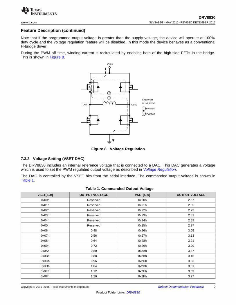
During PWM regulation, the H-bridge is enabled to drive current through the motor winding during the PWM ontime. This is shown in Figure 8 as case 1. The current flow direction shown indicates the state when IN1 is highand IN2 is low.
8 Submit Documentation Feedback Copyright © 2010–2015, Texas Instruments Incorporated
Product Folder Links: DRV8830
OUT1 OUT2
2
1
2
PWM on
PWM off
VCC
1Shown with
IN1=1, IN2=0
DRV8830www.ti.com SLVSAB2G –MAY 2010–REVISED DECEMBER 2015
Feature Description (continued)Note that if the programmed output voltage is greater than the supply voltage, the device will operate at 100%duty cycle and the voltage regulation feature will be disabled. In this mode the device behaves as a conventionalH-bridge driver.
During the PWM off time, winding current is recirculated by enabling both of the high-side FETs in the bridge.This is shown in Figure 8.
Figure 8. Voltage Regulation
7.3.2 Voltage Setting (VSET DAC)The DRV8830 includes an internal reference voltage that is connected to a DAC. This DAC generates a voltagewhich is used to set the PWM regulated output voltage as described in Voltage Regulation.
The DAC is controlled by the VSET bits from the serial interface. The commanded output voltage is shown inTable 1.
Table 1. Commanded Output VoltageVSET[5..0] OUTPUT VOLTAGE VSET[5..0] OUTPUT VOLTAGE
0x00h Reserved 0x20h 2.570x01h Reserved 0x21h 2.650x02h Reserved 0x22h 2.730x03h Reserved 0x23h 2.810x04h Reserved 0x24h 2.890x05h Reserved 0x25h 2.970x06h 0.48 0x26h 3.050x07h 0.56 0x27h 3.130x08h 0.64 0x28h 3.210x09h 0.72 0x29h 3.290x0Ah 0.80 0x2Ah 3.370x0Bh 0.88 0x2Bh 3.450x0Ch 0.96 0x2Ch 3.530x0Dh 1.04 0x2Dh 3.610x0Eh 1.12 0x2Eh 3.690x0Fh 1.20 0x2Fh 3.77
Copyright © 2010–2015, Texas Instruments Incorporated Submit Documentation Feedback 9
Product Folder Links: DRV8830
R =ISENSE
200 mV¾
ILIMIT
DRV8830SLVSAB2G –MAY 2010–REVISED DECEMBER 2015 www.ti.com
Feature Description (continued)Table 1. Commanded Output Voltage (continued)
VSET[5..0] OUTPUT VOLTAGE VSET[5..0] OUTPUT VOLTAGE0x10h 1.29 0x30h 3.860x11h 1.37 0x31h 3.940x12h 1.45 0x32h 4.020x13h 1.53 0x33h 4.10x14h 1.61 0x34h 4.180x15h 1.69 0x35h 4.260x16h 1.77 0x36h 4.340x17h 1.85 0x37h 4.420x18h 1.93 0x38h 4.50x19h 2.01 0x39h 4.580x1Ah 2.09 0x3Ah 4.660x1Bh 2.17 0x3Bh 4.740x1Ch 2.25 0x3Ch 4.820x1Dh 2.33 0x3Dh 4.90x1Eh 2.41 0x3Eh 4.980x1Fh 2.49 0x3Fh 5.06
The voltage can be calculated as 4 x VREF x (VSET +1) / 64, where VREF is the internal 1.285-V reference.
7.3.3 Current LimitA current limit circuit is provided to protect the system in the event of an overcurrent condition, such as whatwould be encountered if driving a DC motor at start-up or with an abnormal mechanical load (stall condition).
The motor current is sensed by monitoring the voltage across an external sense resistor. When the voltageexceeds a reference voltage of 200 mV for more than approximately 3 µs, the PWM duty cycle is reduced to limitthe current through the motor to this value. This current limit allows for starting the motor while controlling thecurrent.
If the current limit condition persists for some time, it is likely that a fault condition has been encountered, suchas the motor being run into a stop or a stalled condition. An overcurrent event must persist for approximately275 ms before the fault is registered. After approximately 275 ms, a fault signaled to the host by driving theFAULTn signal low and setting the FAULT and ILIMIT bits in the serial interface register. Operation of the motordriver will continue.
The current limit fault condition is cleared by setting both IN1 and IN2 to zero to disable the motor current, byputting the device into the shutdown state (IN1 and IN2 both set to 1), by setting the CLEAR bit in the faultregister, or by removing and re-applying power to the device.
The resistor used to set the current limit must be less than 1 Ω. Its value may be calculated as follows:
where• RISENSE is the current sense resistor value.• ILIMIT is the desired current limit (in mA). (1)
If the current limit feature is not needed, the ISENSE pin may be directly connected to ground.
7.3.4 Protection CircuitsThe DRV8830 is fully protected against undervoltage, overcurrent and overtemperature events. A FAULTn pin isavailable to signal a fault condition to the system, as well as a FAULT register in the serial interface that allowsdetermination of the fault source.
10 Submit Documentation Feedback Copyright © 2010–2015, Texas Instruments Incorporated
Product Folder Links: DRV8830
DRV8830www.ti.com SLVSAB2G –MAY 2010–REVISED DECEMBER 2015
7.3.4.1 Overcurrent Protection (OCP)An analog current limit circuit on each FET limits the current through the FET by removing the gate drive. If thisanalog current limit persists for longer than the OCP time, all FETs in the H-bridge will be disabled, the FAULTnsignal will be driven low, and the FAULT and OCP bits in the FAULT register will be set. The device will remaindisabled until the CLEAR bit in the FAULT register is written to 1, or VCC is removed and re-applied.
Overcurrent conditions are sensed independently on both high and low side devices. A short to ground, supply,or across the motor winding will all result in an overcurrent shutdown. Note that OCP is independent of thecurrent limit function, which is typically set to engage at a lower current level; the OCP function is intended toprevent damage to the device under abnormal (for example, short circuit) conditions.
7.3.4.2 Thermal Shutdown (TSD)If the die temperature exceeds safe limits, all FETs in the H-bridge will be disabled, the FAULTn signal will bedriven low, and the FAULT and OTS bits in the serial interface register will be set. Once the die temperature hasfallen to a safe level operation will automatically resume.
7.3.4.3 Undervoltage Lockout (UVLO)If at any time the voltage on the VCC pins falls below the undervoltage lockout threshold voltage, all FETs in theH-bridge will be disabled, the FAULTn signal will be driven low, and the FAULT and UVLO bits in the FAULTregister will be set. Operation will resume when VCC rises above the UVLO threshold.
Table 2. Device ProtectionFAULT CONDITION ERROR REPORT H-BRIDGE INTERNAL CIRCUITS RECOVERY
VCC undervoltage VCC < VUVLO FAULTn Disabled Disabled VCC > VUVLO(UVLO)Overcurret (OCP) IOUT > IOCP FAULT n Disabled Operating Power cycle VCCThermal shutdown TJ > TTSD FAULTn Disabled Operating TJ > TTSD – THYS(TSD)
7.4 Device Functional ModesThe DRV8830 is active when either IN1 or IN2 are set to a logic high. Sleep mode is entered when both IN1 andIN2 are set to a logic low. When in sleep mode, the H-bridge FETs are disabled (Hi-Z).
Table 3. Modes of OperationFAULT CONDITION H-BRIDGE INTERNAL CIRCUITS
Operating IN1 or IN2 high Operating OperatingSleep mode IN1 or IN2 low Disabled Diabled
Fault encountered Any fault condition met Disabled See Table 2
7.4.1 Bridge ControlThe IN1 and IN2 control bits in the serial interface register enable the H-bridge outputs. Table 4 shows the logic:
Table 4. H-Bridge LogicIN1 IN2 OUT1 OUT2 FUNCTION0 0 Z Z Standby / coast0 1 L H Reverse1 0 H L Forward1 1 H H Brake
Copyright © 2010–2015, Texas Instruments Incorporated Submit Documentation Feedback 11
Product Folder Links: DRV8830
DRV8830SLVSAB2G –MAY 2010–REVISED DECEMBER 2015 www.ti.com
When both bits are zero, the output drivers are disabled and the device is placed into a low-power shutdownstate. The current limit fault condition (if present) is also cleared.
At initial power up, the device will enter the low-power shutdown state. Note that when transitioning from eitherbrake or standby mode to forward or reverse, the voltage control PWM starts at zero duty cycle. The duty cycleslowly ramps up to the commanded voltage. This can take up to 12 ms to go from standby to 100% duty cycle.
7.5 Programming
7.5.1 I2C-Compatible Serial InterfaceThe I2C interface allows control and monitoring of the DRV8830 by a microcontroller. I2C is a two-wire serialinterface developed by Philips Semiconductor (see I2C – Bus Specification, Version 2.1, January 2000). The busconsists of a data line (SDA) and a clock line (SCL) with off-chip pull-up resistors. When the bus is idle, bothSDA and SCL lines are pulled high.
A master device, usually a microcontroller or a digital signal processor, controls the bus. The master isresponsible for generating the SCL signal and device addresses. The master also generates specific conditionsthat indicate the START and STOP of data transfer.
A slave device receives and/or transmits data on the bus under control of the master device. This deviceoperates only as a slave device.
I2C communication is initiated by a master sending a start condition, a high-to-low transition on the SDA I/O whileSCL is held high. After the start condition, the device address byte is sent, most-significant bit (MSB) first,including the data direction bit (R/W). After receiving a valid address byte, this device responds with anacknowledge, a low on the SDA I/O during the high of the acknowledge-related clock pulse.
The lower three bits of the device address are input from pins A0 - A1, which can be tied to VCC (logic high),GND (logic low), or left open. These three address bits are latched into the device at power up, so cannot bechanged dynamically.
The upper address bits of the device address are fixed at 0xC0h, so the device address is as follows:
Table 5. Device AddressesA3..A0 BITSA1 PIN A0 PIN ADDRESS (WRITE) ADDRESS (READ)(as below)
0 0 0000 0xC0h 0xC1h0 open 0001 0xC2h 0xC3h0 1 0010 0xC4h 0xC5h
open 0 0011 0xC6h 0xC7hopen open 0100 0xC8h 0xC9hopen 1 0101 0xCAh 0xCBh
1 0 0110 0xCCh 0xCDh1 open 0111 0xCEh 0xCFh1 1 1000 0xD0h 0xD1h
The DRV8830 does not respond to the general call address.
A data byte follows the address acknowledge. If the R/W bit is low, the data is written from the master. If the R/Wbit is high, the data from this device are the values read from the register previously selected by a write to thesubaddress register. The data byte is followed by an acknowledge sent from this device. Data is output only ifcomplete bytes are received and acknowledged. A stop condition, which is a low-to-high transition on the SDAI/O while the SCL input is high, is sent by the master to terminate the transfer.
A master bus device must wait at least 60 μs after power is applied to VCC to generate a START condition.
I2C transactions are shown in the timing diagrams Figure 9 and Figure 10:
12 Submit Documentation Feedback Copyright © 2010–2015, Texas Instruments Incorporated
Product Folder Links: DRV8830
S
1 1
0
(As) (An)
W
STA
RT
Slave
Address AC
K Sub
Address AC
K
(Dn) (Dn+1)
Data
AC
K
Data
AC
K
ST
OP
S
1 1
0
(As) (An)
W
S
1 1
0
(As) (Dn)
R
(Dn+1)S
TA
RT
Slave
Address AC
K Sub
Address AC
KS
TA
RT
Slave
Address AC
K
Data
AC
K
Data
AC
K
ST
OP
DRV8830www.ti.com SLVSAB2G –MAY 2010–REVISED DECEMBER 2015
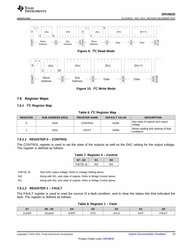
Figure 9. I2C Read Mode
Figure 10. I2C Write Mode
7.6 Register Maps
7.6.1 I2C Register Map
Table 6. I2C Register MapREGISTER SUB ADDRESS (HEX) REGISTER NAME DEFAULT VALUE DESCRIPTION
Sets state of outputs and output0 0x00 CONTROL 0x00h voltageAllows reading and clearing of fault1 0x01 FAULT 0x00h conditions
7.6.1.1 REGISTER 0 – CONTROLThe CONTROL register is used to set the state of the outputs as well as the DAC setting for the output voltage.The register is defined as follows:
Table 7. Register 0 – ControlD7 - D2 D1 D0
VSET[5..0] IN2 IN1
VSET[5..0]: Sets DAC output voltage. Refer to Voltage Setting above.IN2: Along with IN1, sets state of outputs. Refer to Bridge Control above.IN1: Along with IN2, sets state of outputs. Refer to Bridge Control above.
7.6.1.2 REGISTER 1 – FAULTThe FAULT register is used to read the source of a fault condition, and to clear the status bits that indicated thefault. The register is defined as follows:
Table 8. Register 1 – FaultD7 D6 - D5 D4 D3 D2 D1 D0
CLEAR Unused ILIMIT OTS UVLO OCP FAULT
Copyright © 2010–2015, Texas Instruments Incorporated Submit Documentation Feedback 13
Product Folder Links: DRV8830
DRV8830SLVSAB2G –MAY 2010–REVISED DECEMBER 2015 www.ti.com
CLEAR: When written to 1, clears the fault status bitsILIMIT: If set, indicates the fault was caused by an extended current limit eventOTS: If set, indicates that the fault was caused by an overtemperature (OTS) conditionUVLO: If set, indicates the fault was caused by an undervoltage lockoutOCP: If set, indicates the fault was caused by an overcurrent (OCP) eventFAULT: Set if any fault condition exists
14 Submit Documentation Feedback Copyright © 2010–2015, Texas Instruments Incorporated
Product Folder Links: DRV8830
OUT1
GND
SCL
OUT2
SDA
A1
A0
BDC
FAULTn
VCC
VCC
10 µF
Controller
PPAD
ISENSE
0.4
2.87k
10k
DRV8830www.ti.com SLVSAB2G –MAY 2010–REVISED DECEMBER 2015
8 Application and Implementation
NOTEInformation in the following applications sections is not part of the TI componentspecification, and TI does not warrant its accuracy or completeness. TI’s customers areresponsible for determining suitability of components for their purposes. Customers shouldvalidate and test their design implementation to confirm system functionality.
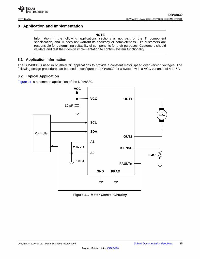
8.1 Application InformationThe DRV8830 is used in brushed DC applications to provide a constant motor speed over varying voltages. Thefollowing design procedure can be used to configure the DRV8830 for a system with a VCC variance of 4 to 6 V.
8.2 Typical ApplicationFigure 11 is a common application of the DRV8830.
Figure 11. Motor Control Circuitry
Copyright © 2010–2015, Texas Instruments Incorporated Submit Documentation Feedback 15
Product Folder Links: DRV8830
DRV8830SLVSAB2G –MAY 2010–REVISED DECEMBER 2015 www.ti.com
Typical Application (continued)8.2.1 Design RequirementsTable 9 lists the design parameters of the DRV8830.
Table 9. Design ParametersDESIGN REFERENCE EXAMPLE VALUEPARAMETER
Motor voltage VCC 5 VMotor RMS current IRMS 0.3 A
Motor start-up ISTART 1.3 AMotor current trip ILIMIT 0.9 Apoint
8.2.2 Detailed Design Procedure
8.2.2.1 Motor VoltageThe motor voltage to use will depend on the ratings of the motor selected and the desired RPM. A higher voltagespins a brushed DC motor faster with the same PWM duty cycle applied to the power FETs. A higher voltagealso increases the rate of current change through the inductive motor windings.
For the DRV8830, TI recommends to set a motor voltage at the lowest system VCC. This will maintain a constantRPM across varying VCC conditions.
For example if the VCC voltage can vary from 4.5V to 5.5V, setting the VSET voltage to 1.125 V will compensatefor power supply variation. The DRV8830 will set the motor voltage at 4.5 V, even if VCC is 5.5 V.
8.2.2.2 Motor Current Trip PointWhen the voltage on pin ISENSE exceeds VILIM (0.2 V), overcurrent is detected. The RSENSE resistor shouldbe sized to set the desired ILIMIT level.
RISENSE = 0.2 V / ILIMIT (2)
To set IILIMIT to 0.5 A, RISENSE = 0.2 V / 0.9 A = 0.22 Ω.
To prevent false trips, ILIMIT must be higher than regular operating current. Motor current during start-up istypically much higher than steady-state spinning, because the initial load torque is higher, and the absence ofback-EMF causes a higher voltage and extra current across the motor windings.
It can be beneficial to limit start-up current by using series inductors on the DRV8830 output, as that allows ILIMITto be lower, and it may decrease the system’s required bulk capacitance. Start-up current can also be limited byramping the forward drive duty cycle.
8.2.2.3 Sense Resistor SelectionFor optimal performance, it is important for the sense resistor to be:• Surface-mount• Low inductance• Rated for high enough power• Placed closely to the motor driver
The power dissipated by the sense resistor equals IRMS2 × R. For example, if peak motor current is 1 A, RMSmotor current is 0.7 A, and a 0.4-Ω sense resistor is used, the resistor will dissipate 0.7 A2 × 0.4 Ω = 0.2 W. Thepower quickly increases with higher current levels.
Resistors typically have a rated power within some ambient temperature range, along with a de-rated powercurve for high ambient temperatures. When a PCB is shared with other components generating heat, marginshould be added. It is always best to measure the actual sense resistor temperature in a final system, along withthe power MOSFETs, as those are often the hottest components.
16 Submit Documentation Feedback Copyright © 2010–2015, Texas Instruments Incorporated
Product Folder Links: DRV8830
DRV8830www.ti.com SLVSAB2G –MAY 2010–REVISED DECEMBER 2015
Because power resistors are larger and more expensive than standard resistors, it is common practice to usemultiple standard resistors in parallel, between the sense node and ground. This distributes the current and heatdissipation.
8.2.2.4 Low Power OperationUnder normal operation, using sleep mode to minimize supply current should be sufficient.
If desired, power can be removed to the DRV8830 to further decrease supply current. TI recommends to removepower to the FAULTn pullup resistor when removing power to the DRV8830. Removing power from the FAULTnpullup resistor will eliminate a current path from the FAULTn pin through an ESD protection diode to VCC. TIrecommends to set both IN1 and IN2 as a logic low when power is removed.
An undervoltage event may cause the address to be re-evaluated. If this occurs, the I2C interface may stopworking until power is cycled.
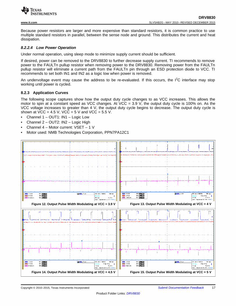
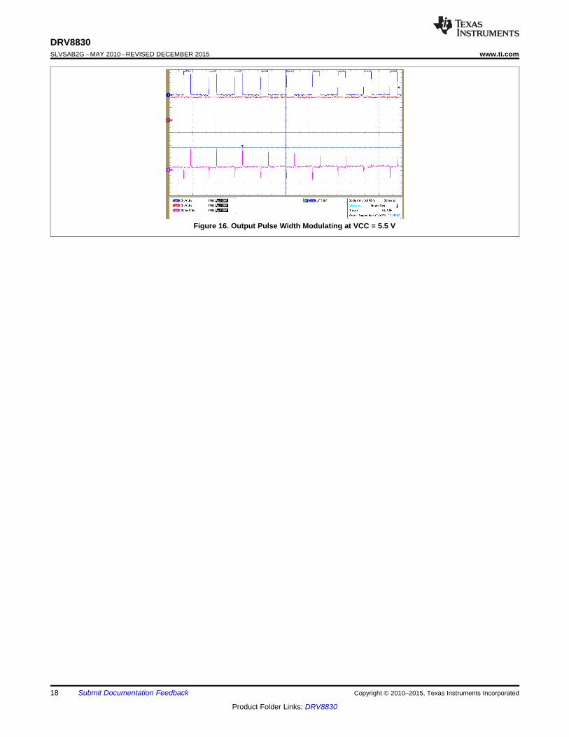
8.2.3 Application CurvesThe following scope captures show how the output duty cycle changes to as VCC increases. This allows themotor to spin at a constant speed as VCC changes. At VCC = 3.9 V, the output duty cycle is 100% on. As theVCC voltage increases to greater than 4 V, the output duty cycle begins to decrease. The output duty cycle isshown at VCC = 4.5 V, VCC = 5 V and VCC = 5.5 V.• Channel 1 – OUT1: IN1 – Logic Low• Channel 2 – OUT2: IN2 – Logic High• Channel 4 – Motor current: VSET – 1 V• Motor used: NMB Technologies Corporation, PPN7PA12C1
Figure 13. Output Pulse Width Modulating at VCC = 4 VFigure 12. Output Pulse Width Modulating at VCC = 3.9 V
Figure 14. Output Pulse Width Modulating at VCC = 4.5 V Figure 15. Output Pulse Width Modulating at VCC = 5 V
Copyright © 2010–2015, Texas Instruments Incorporated Submit Documentation Feedback 17
Product Folder Links: DRV8830
DRV8830SLVSAB2G –MAY 2010–REVISED DECEMBER 2015 www.ti.com
Figure 16. Output Pulse Width Modulating at VCC = 5.5 V
18 Submit Documentation Feedback Copyright © 2010–2015, Texas Instruments Incorporated
Product Folder Links: DRV8830
Local Bulk Capacitor
Parasitic WireInductance
++
±±Motor Driver
Power Supply Motor Drive System
VCC
GND
+
IC Bypass Capacitor
DRV8830www.ti.com SLVSAB2G –MAY 2010–REVISED DECEMBER 2015
9 Power Supply Recommendations
9.1 Power SupervisorThe DRV8830 is capable of entering a low-power sleep mode by bringing both of the INx control inputs logic low.The outputs will be disabled Hi-Z.
To exit the sleep mode, bring either or both of the INx inputs logic high. This will enable the H-bridges. Whenexiting the sleep mode, the FAULTn pin will pulse low.
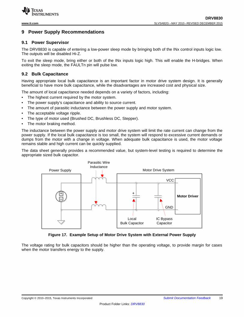
9.2 Bulk CapacitanceHaving appropriate local bulk capacitance is an important factor in motor drive system design. It is generallybeneficial to have more bulk capacitance, while the disadvantages are increased cost and physical size.
The amount of local capacitance needed depends on a variety of factors, including:• The highest current required by the motor system.• The power supply’s capacitance and ability to source current.• The amount of parasitic inductance between the power supply and motor system.• The acceptable voltage ripple.• The type of motor used (Brushed DC, Brushless DC, Stepper).• The motor braking method.
The inductance between the power supply and motor drive system will limit the rate current can change from thepower supply. If the local bulk capacitance is too small, the system will respond to excessive current demands ordumps from the motor with a change in voltage. When adequate bulk capacitance is used, the motor voltageremains stable and high current can be quickly supplied.
The data sheet generally provides a recommended value, but system-level testing is required to determine theappropriate sized bulk capacitor.
Figure 17. Example Setup of Motor Drive System with External Power Supply
The voltage rating for bulk capacitors should be higher than the operating voltage, to provide margin for caseswhen the motor transfers energy to the supply.
Copyright © 2010–2015, Texas Instruments Incorporated Submit Documentation Feedback 19
Product Folder Links: DRV8830
P = R (I )TOT DS(ON) OUT(RMS)22
· ·
OUT2
ISENSE
OUT1
VCC
GND
SCL
SDA
A1
A0
10 µFFAULTn
DRV8830SLVSAB2G –MAY 2010–REVISED DECEMBER 2015 www.ti.com
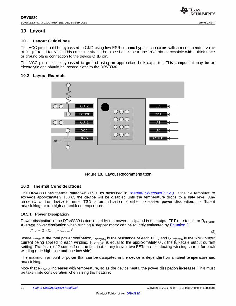
10 Layout
10.1 Layout GuidelinesThe VCC pin should be bypassed to GND using low-ESR ceramic bypass capacitors with a recommended valueof 0.1-μF rated for VCC. This capacitor should be placed as close to the VCC pin as possible with a thick traceor ground plane connection to the device GND pin.
The VCC pin must be bypassed to ground using an appropriate bulk capacitor. This component may be anelectrolytic and should be located close to the DRV8830.
10.2 Layout Example
Figure 18. Layout Recommendation
10.3 Thermal ConsiderationsThe DRV8830 has thermal shutdown (TSD) as described in Thermal Shutdown (TSD). If the die temperatureexceeds approximately 160°C, the device will be disabled until the temperature drops to a safe level. Anytendency of the device to enter TSD is an indication of either excessive power dissipation, insufficientheatsinking, or too high an ambient temperature.
10.3.1 Power DissipationPower dissipation in the DRV8830 is dominated by the power dissipated in the output FET resistance, or RDS(ON).Average power dissipation when running a stepper motor can be roughly estimated by Equation 3.
(3)
where PTOT is the total power dissipation, RDS(ON) is the resistance of each FET, and IOUT(RMS) is the RMS outputcurrent being applied to each winding. IOUT(RMS) is equal to the approximately 0.7x the full-scale output currentsetting. The factor of 2 comes from the fact that at any instant two FETs are conducting winding current for eachwinding (one high-side and one low-side).
The maximum amount of power that can be dissipated in the device is dependent on ambient temperature andheatsinking.
Note that RDS(ON) increases with temperature, so as the device heats, the power dissipation increases. This mustbe taken into consideration when sizing the heatsink.
20 Submit Documentation Feedback Copyright © 2010–2015, Texas Instruments Incorporated
Product Folder Links: DRV8830
DRV8830www.ti.com SLVSAB2G –MAY 2010–REVISED DECEMBER 2015
11 Device and Documentation Support
11.1 Documentation Support
11.1.1 Related DocumentationFor related documentation, see the following:• PowerPAD™ Thermally Enhanced Package, SLMA002• PowerPAD™ Made Easy, SLMA004
11.2 Community ResourcesThe following links connect to TI community resources. Linked contents are provided "AS IS" by the respectivecontributors. They do not constitute TI specifications and do not necessarily reflect TI's views; see TI's Terms ofUse.
TI E2E™ Online Community TI's Engineer-to-Engineer (E2E) Community. Created to foster collaborationamong engineers. At e2e.ti.com, you can ask questions, share knowledge, explore ideas and helpsolve problems with fellow engineers.
Design Support TI's Design Support Quickly find helpful E2E forums along with design support tools andcontact information for technical support.
11.3 TrademarksPowerPAD, E2E are trademarks of Texas Instruments.All other trademarks are the property of their respective owners.
11.4 Electrostatic Discharge CautionThese devices have limited built-in ESD protection. The leads should be shorted together or the device placed in conductive foamduring storage or handling to prevent electrostatic damage to the MOS gates.
11.5 GlossarySLYZ022 — TI Glossary.
This glossary lists and explains terms, acronyms, and definitions.
12 Mechanical, Packaging, and Orderable InformationThe following pages include mechanical, packaging, and orderable information. This information is the mostcurrent data available for the designated devices. This data is subject to change without notice and revision ofthis document. For browser-based versions of this data sheet, refer to the left-hand navigation.
Copyright © 2010–2015, Texas Instruments Incorporated Submit Documentation Feedback 21
Product Folder Links: DRV8830
PACKAGE OPTION ADDENDUM
www.ti.com 10-Oct-2014
Addendum-Page 1
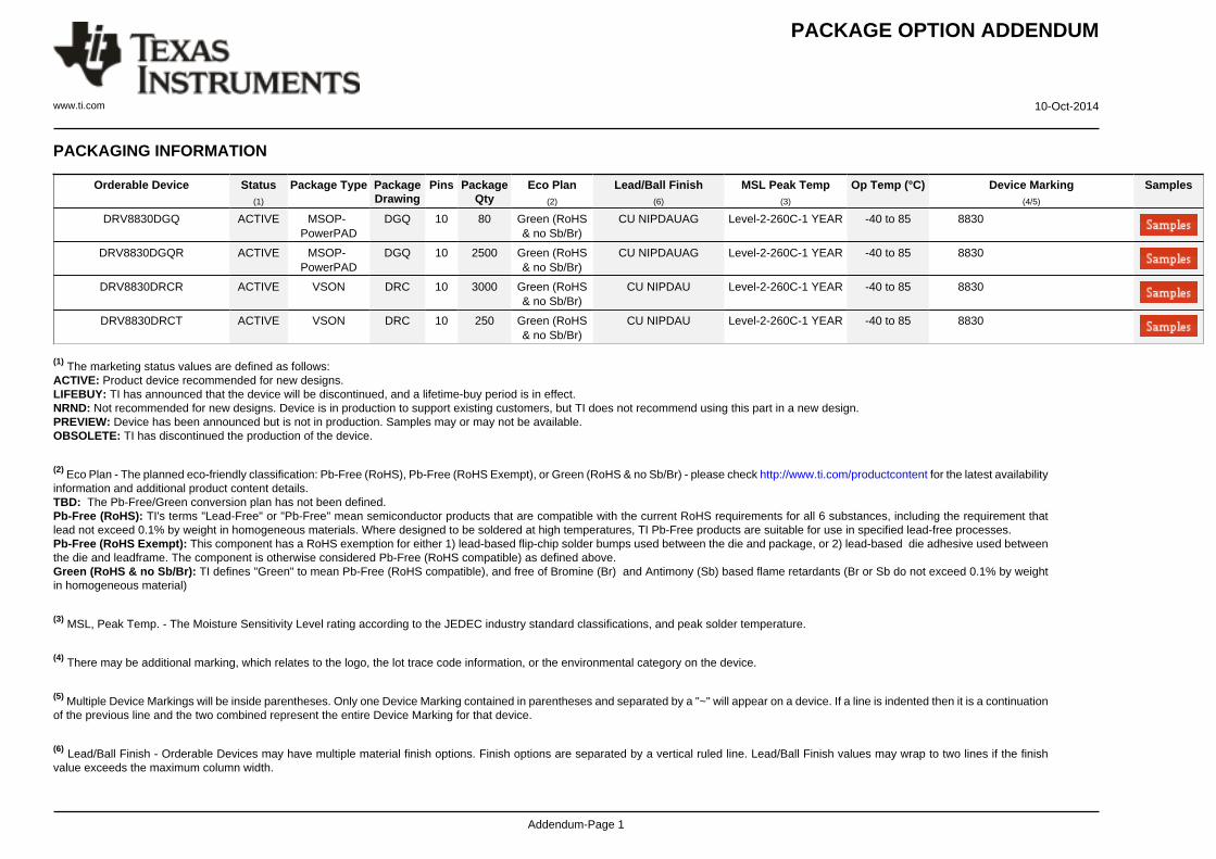
PACKAGING INFORMATION
Orderable Device Status(1)
Package Type PackageDrawing
Pins PackageQty
Eco Plan(2)
Lead/Ball Finish(6)
MSL Peak Temp(3)
Op Temp (°C) Device Marking(4/5)
Samples
DRV8830DGQ ACTIVE MSOP-PowerPAD
DGQ 10 80 Green (RoHS& no Sb/Br)
CU NIPDAUAG Level-2-260C-1 YEAR -40 to 85 8830
DRV8830DGQR ACTIVE MSOP-PowerPAD
DGQ 10 2500 Green (RoHS& no Sb/Br)
CU NIPDAUAG Level-2-260C-1 YEAR -40 to 85 8830
DRV8830DRCR ACTIVE VSON DRC 10 3000 Green (RoHS& no Sb/Br)
CU NIPDAU Level-2-260C-1 YEAR -40 to 85 8830
DRV8830DRCT ACTIVE VSON DRC 10 250 Green (RoHS& no Sb/Br)
CU NIPDAU Level-2-260C-1 YEAR -40 to 85 8830
(1) The marketing status values are defined as follows:ACTIVE: Product device recommended for new designs.LIFEBUY: TI has announced that the device will be discontinued, and a lifetime-buy period is in effect.NRND: Not recommended for new designs. Device is in production to support existing customers, but TI does not recommend using this part in a new design.PREVIEW: Device has been announced but is not in production. Samples may or may not be available.OBSOLETE: TI has discontinued the production of the device.
(2) Eco Plan - The planned eco-friendly classification: Pb-Free (RoHS), Pb-Free (RoHS Exempt), or Green (RoHS & no Sb/Br) - please check http://www.ti.com/productcontent for the latest availabilityinformation and additional product content details.TBD: The Pb-Free/Green conversion plan has not been defined.Pb-Free (RoHS): TI's terms "Lead-Free" or "Pb-Free" mean semiconductor products that are compatible with the current RoHS requirements for all 6 substances, including the requirement thatlead not exceed 0.1% by weight in homogeneous materials. Where designed to be soldered at high temperatures, TI Pb-Free products are suitable for use in specified lead-free processes.Pb-Free (RoHS Exempt): This component has a RoHS exemption for either 1) lead-based flip-chip solder bumps used between the die and package, or 2) lead-based die adhesive used betweenthe die and leadframe. The component is otherwise considered Pb-Free (RoHS compatible) as defined above.Green (RoHS & no Sb/Br): TI defines "Green" to mean Pb-Free (RoHS compatible), and free of Bromine (Br) and Antimony (Sb) based flame retardants (Br or Sb do not exceed 0.1% by weightin homogeneous material)
(3) MSL, Peak Temp. - The Moisture Sensitivity Level rating according to the JEDEC industry standard classifications, and peak solder temperature.
(4) There may be additional marking, which relates to the logo, the lot trace code information, or the environmental category on the device.
(5) Multiple Device Markings will be inside parentheses. Only one Device Marking contained in parentheses and separated by a "~" will appear on a device. If a line is indented then it is a continuationof the previous line and the two combined represent the entire Device Marking for that device.
(6) Lead/Ball Finish - Orderable Devices may have multiple material finish options. Finish options are separated by a vertical ruled line. Lead/Ball Finish values may wrap to two lines if the finishvalue exceeds the maximum column width.
PACKAGE OPTION ADDENDUM
www.ti.com 10-Oct-2014
Addendum-Page 2
Important Information and Disclaimer:The information provided on this page represents TI's knowledge and belief as of the date that it is provided. TI bases its knowledge and belief on informationprovided by third parties, and makes no representation or warranty as to the accuracy of such information. Efforts are underway to better integrate information from third parties. TI has taken andcontinues to take reasonable steps to provide representative and accurate information but may not have conducted destructive testing or chemical analysis on incoming materials and chemicals.TI and TI suppliers consider certain information to be proprietary, and thus CAS numbers and other limited information may not be available for release.
In no event shall TI's liability arising out of such information exceed the total purchase price of the TI part(s) at issue in this document sold by TI to Customer on an annual basis.
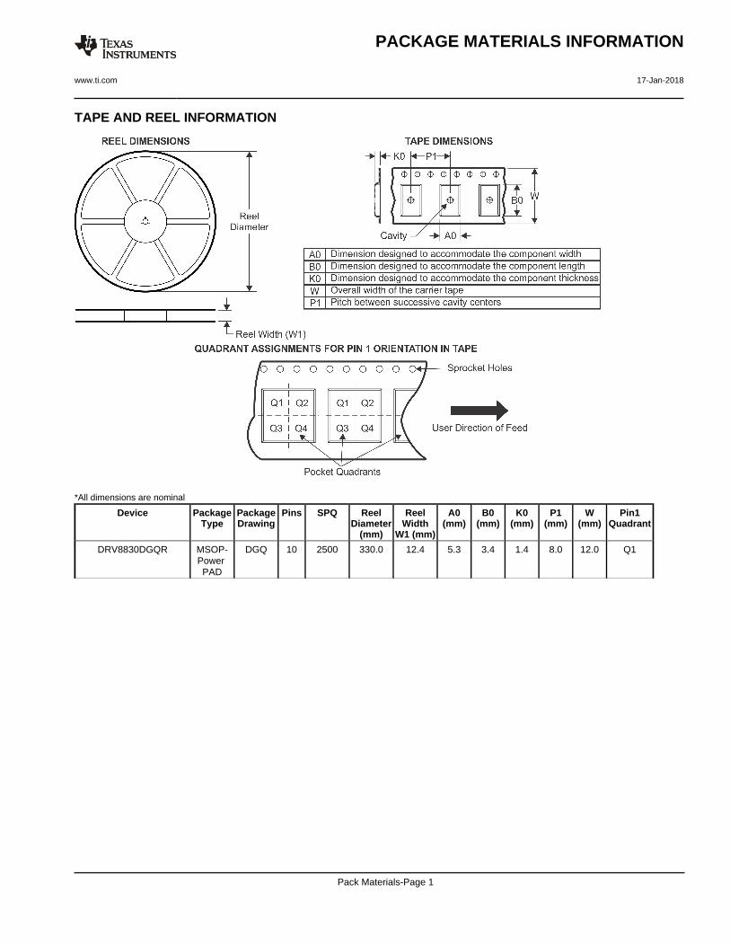
TAPE AND REEL INFORMATION
*All dimensions are nominal
Device PackageType
PackageDrawing
Pins SPQ ReelDiameter
(mm)
ReelWidth
W1 (mm)
A0(mm)
B0(mm)
K0(mm)
P1(mm)
W(mm)
Pin1Quadrant
DRV8830DGQR MSOP-Power PAD
DGQ 10 2500 330.0 12.4 5.3 3.4 1.4 8.0 12.0 Q1
PACKAGE MATERIALS INFORMATION
www.ti.com 17-Jan-2018
Pack Materials-Page 1
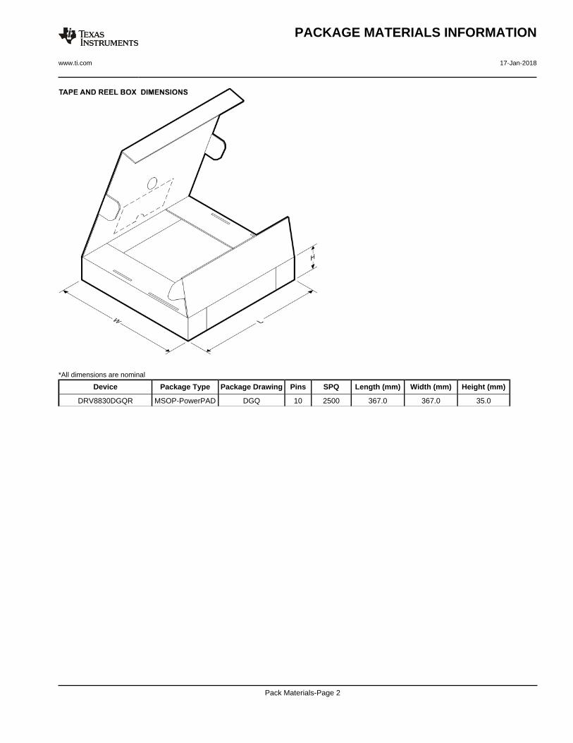
*All dimensions are nominal
Device Package Type Package Drawing Pins SPQ Length (mm) Width (mm) Height (mm)
DRV8830DGQR MSOP-PowerPAD DGQ 10 2500 367.0 367.0 35.0
PACKAGE MATERIALS INFORMATION
www.ti.com 17-Jan-2018
Pack Materials-Page 2
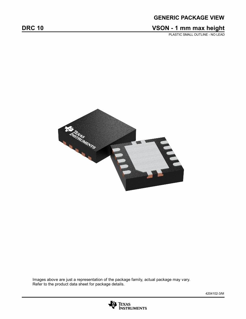
GENERIC PACKAGE VIEW
Images above are just a representation of the package family, actual package may vary.Refer to the product data sheet for package details.
DRC 10 VSON - 1 mm max heightPLASTIC SMALL OUTLINE - NO LEAD
4204102-3/M
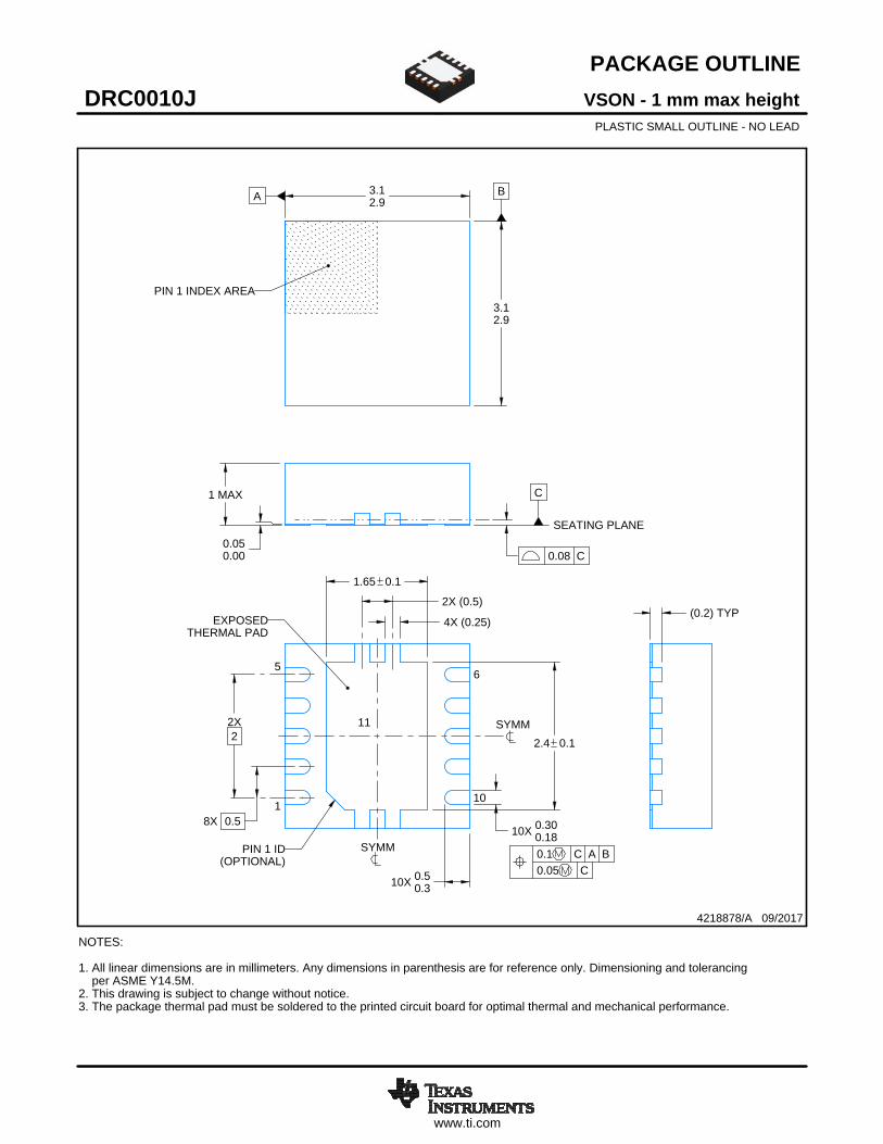
www.ti.com
PACKAGE OUTLINE
C
10X 0.300.18
2.4 0.1
2X2
1.65 0.1
8X 0.5
1 MAX
10X 0.50.3
0.050.00
A 3.12.9
B
3.12.9
(0.2) TYP4X (0.25)
2X (0.5)
VSON - 1 mm max heightDRC0010JPLASTIC SMALL OUTLINE - NO LEAD
4218878/A 09/2017
PIN 1 INDEX AREA
SEATING PLANE
0.08 C
1
56
10
(OPTIONAL)PIN 1 ID 0.1 C A B
0.05 C
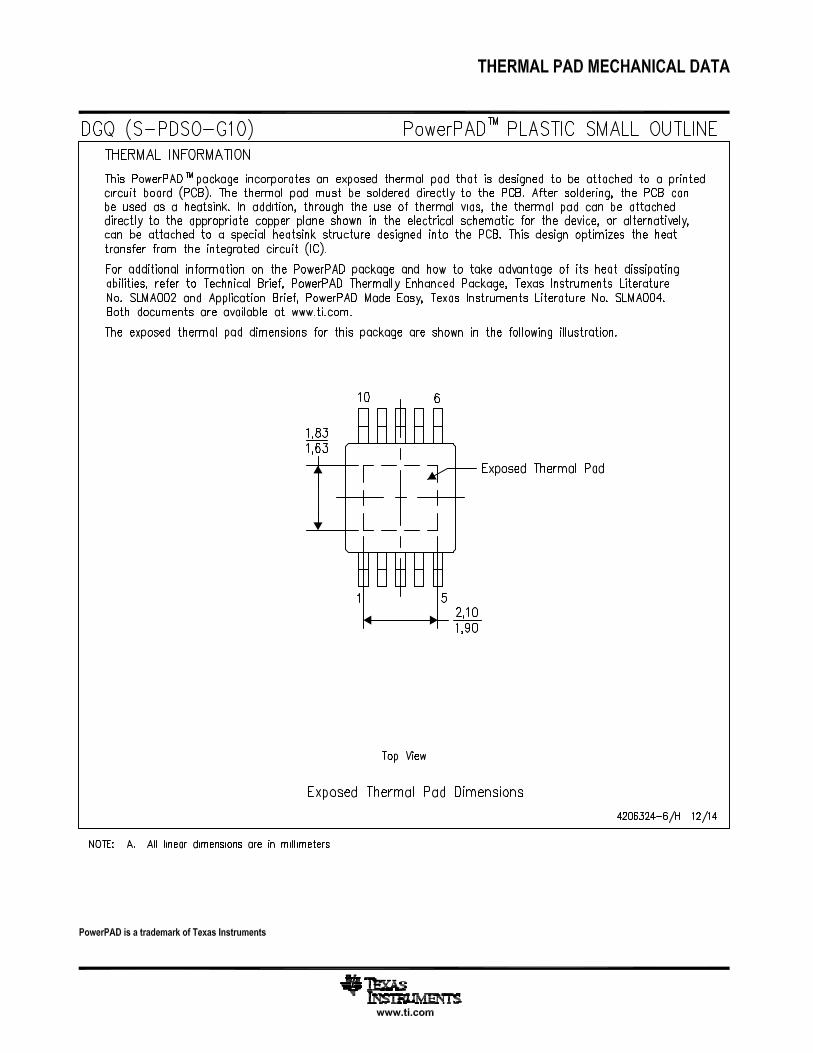
THERMAL PADEXPOSED
SYMM
SYMM11
NOTES: 1. All linear dimensions are in millimeters. Any dimensions in parenthesis are for reference only. Dimensioning and tolerancing per ASME Y14.5M. 2. This drawing is subject to change without notice. 3. The package thermal pad must be soldered to the printed circuit board for optimal thermal and mechanical performance.
SCALE 4.000
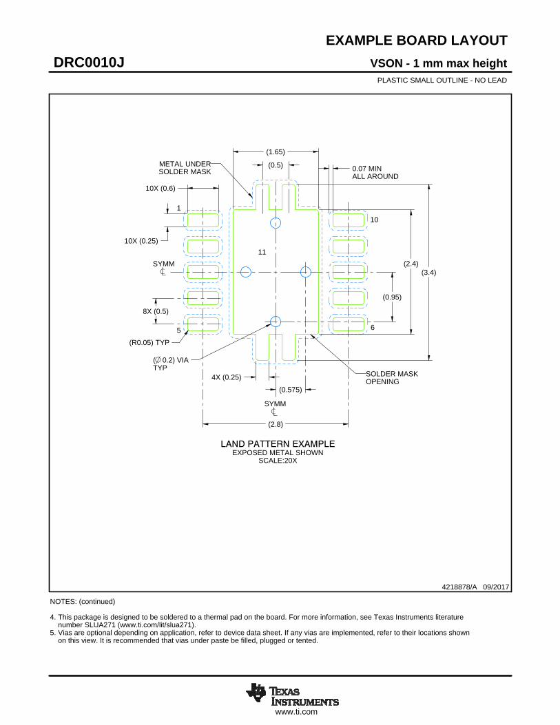
www.ti.com
EXAMPLE BOARD LAYOUT
0.07 MINALL AROUND
10X (0.25)
(2.4)
(2.8)
8X (0.5)
(1.65)
( 0.2) VIATYP
(0.575)
(0.95)
10X (0.6)
(R0.05) TYP
(3.4)
4X (0.25)
(0.5)
VSON - 1 mm max heightDRC0010JPLASTIC SMALL OUTLINE - NO LEAD
4218878/A 09/2017
SYMM
1
5 6
10
LAND PATTERN EXAMPLEEXPOSED METAL SHOWN
SCALE:20X
11SYMM
METAL UNDERSOLDER MASK
SOLDER MASKOPENING
NOTES: (continued) 4. This package is designed to be soldered to a thermal pad on the board. For more information, see Texas Instruments literature number SLUA271 (www.ti.com/lit/slua271).5. Vias are optional depending on application, refer to device data sheet. If any vias are implemented, refer to their locations shown on this view. It is recommended that vias under paste be filled, plugged or tented.
www.ti.com
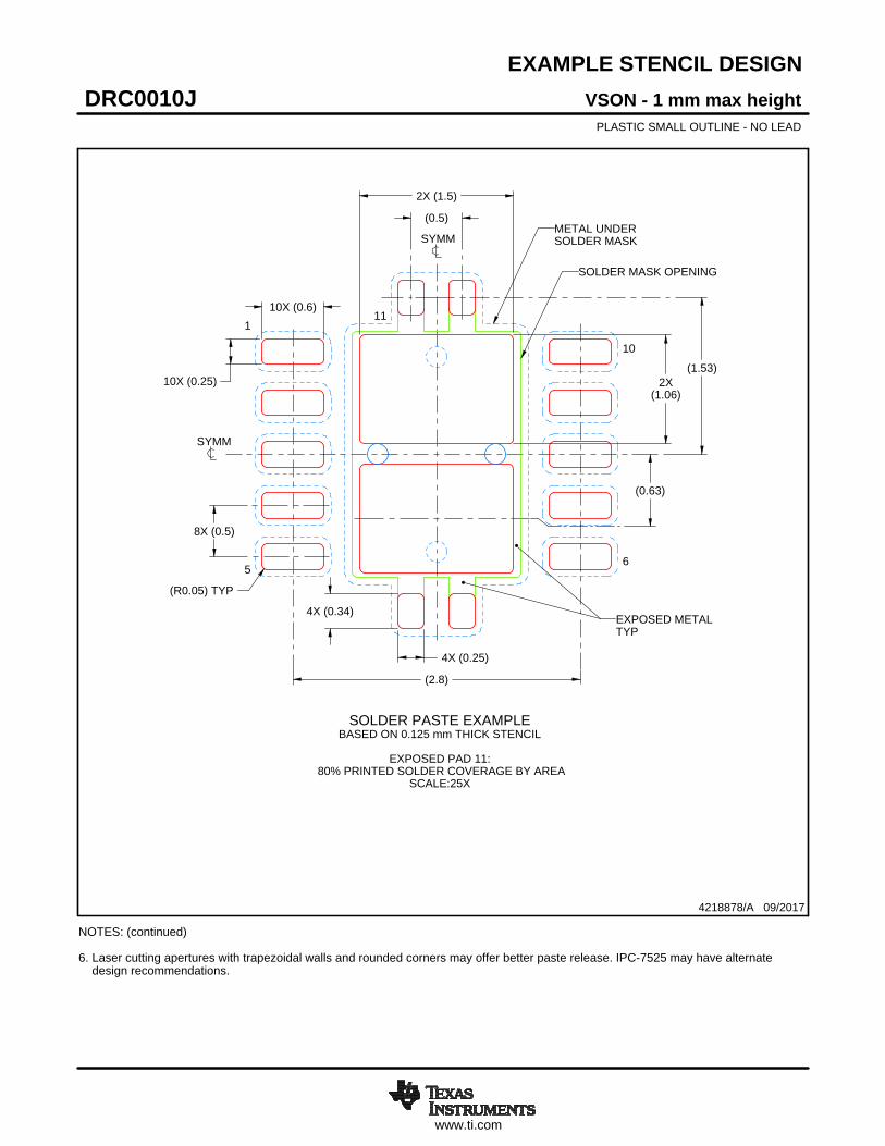
EXAMPLE STENCIL DESIGN
(R0.05) TYP
10X (0.25)
10X (0.6)
2X (1.5)
2X(1.06)
(2.8)
(0.63)
8X (0.5)
(0.5)
4X (0.34)
4X (0.25)
(1.53)
VSON - 1 mm max heightDRC0010JPLASTIC SMALL OUTLINE - NO LEAD
4218878/A 09/2017
NOTES: (continued) 6. Laser cutting apertures with trapezoidal walls and rounded corners may offer better paste release. IPC-7525 may have alternate design recommendations.
SOLDER PASTE EXAMPLEBASED ON 0.125 mm THICK STENCIL
EXPOSED PAD 11:
80% PRINTED SOLDER COVERAGE BY AREASCALE:25X
SYMM
1
56
10
EXPOSED METALTYP
11
SYMM
SOLDER MASK OPENING
METAL UNDERSOLDER MASK
IMPORTANT NOTICE
Texas Instruments Incorporated (TI) reserves the right to make corrections, enhancements, improvements and other changes to itssemiconductor products and services per JESD46, latest issue, and to discontinue any product or service per JESD48, latest issue. Buyersshould obtain the latest relevant information before placing orders and should verify that such information is current and complete.TI’s published terms of sale for semiconductor products (http://www.ti.com/sc/docs/stdterms.htm) apply to the sale of packaged integratedcircuit products that TI has qualified and released to market. Additional terms may apply to the use or sale of other types of TI products andservices.Reproduction of significant portions of TI information in TI data sheets is permissible only if reproduction is without alteration and isaccompanied by all associated warranties, conditions, limitations, and notices. TI is not responsible or liable for such reproduceddocumentation. Information of third parties may be subject to additional restrictions. Resale of TI products or services with statementsdifferent from or beyond the parameters stated by TI for that product or service voids all express and any implied warranties for theassociated TI product or service and is an unfair and deceptive business practice. TI is not responsible or liable for any such statements.Buyers and others who are developing systems that incorporate TI products (collectively, “Designers”) understand and agree that Designersremain responsible for using their independent analysis, evaluation and judgment in designing their applications and that Designers havefull and exclusive responsibility to assure the safety of Designers' applications and compliance of their applications (and of all TI productsused in or for Designers’ applications) with all applicable regulations, laws and other applicable requirements. Designer represents that, withrespect to their applications, Designer has all the necessary expertise to create and implement safeguards that (1) anticipate dangerousconsequences of failures, (2) monitor failures and their consequences, and (3) lessen the likelihood of failures that might cause harm andtake appropriate actions. Designer agrees that prior to using or distributing any applications that include TI products, Designer willthoroughly test such applications and the functionality of such TI products as used in such applications.TI’s provision of technical, application or other design advice, quality characterization, reliability data or other services or information,including, but not limited to, reference designs and materials relating to evaluation modules, (collectively, “TI Resources”) are intended toassist designers who are developing applications that incorporate TI products; by downloading, accessing or using TI Resources in anyway, Designer (individually or, if Designer is acting on behalf of a company, Designer’s company) agrees to use any particular TI Resourcesolely for this purpose and subject to the terms of this Notice.TI’s provision of TI Resources does not expand or otherwise alter TI’s applicable published warranties or warranty disclaimers for TIproducts, and no additional obligations or liabilities arise from TI providing such TI Resources. TI reserves the right to make corrections,enhancements, improvements and other changes to its TI Resources. TI has not conducted any testing other than that specificallydescribed in the published documentation for a particular TI Resource.Designer is authorized to use, copy and modify any individual TI Resource only in connection with the development of applications thatinclude the TI product(s) identified in such TI Resource. NO OTHER LICENSE, EXPRESS OR IMPLIED, BY ESTOPPEL OR OTHERWISETO ANY OTHER TI INTELLECTUAL PROPERTY RIGHT, AND NO LICENSE TO ANY TECHNOLOGY OR INTELLECTUAL PROPERTYRIGHT OF TI OR ANY THIRD PARTY IS GRANTED HEREIN, including but not limited to any patent right, copyright, mask work right, orother intellectual property right relating to any combination, machine, or process in which TI products or services are used. Informationregarding or referencing third-party products or services does not constitute a license to use such products or services, or a warranty orendorsement thereof. Use of TI Resources may require a license from a third party under the patents or other intellectual property of thethird party, or a license from TI under the patents or other intellectual property of TI.TI RESOURCES ARE PROVIDED “AS IS” AND WITH ALL FAULTS. TI DISCLAIMS ALL OTHER WARRANTIES ORREPRESENTATIONS, EXPRESS OR IMPLIED, REGARDING RESOURCES OR USE THEREOF, INCLUDING BUT NOT LIMITED TOACCURACY OR COMPLETENESS, TITLE, ANY EPIDEMIC FAILURE WARRANTY AND ANY IMPLIED WARRANTIES OFMERCHANTABILITY, FITNESS FOR A PARTICULAR PURPOSE, AND NON-INFRINGEMENT OF ANY THIRD PARTY INTELLECTUALPROPERTY RIGHTS. TI SHALL NOT BE LIABLE FOR AND SHALL NOT DEFEND OR INDEMNIFY DESIGNER AGAINST ANY CLAIM,INCLUDING BUT NOT LIMITED TO ANY INFRINGEMENT CLAIM THAT RELATES TO OR IS BASED ON ANY COMBINATION OFPRODUCTS EVEN IF DESCRIBED IN TI RESOURCES OR OTHERWISE. IN NO EVENT SHALL TI BE LIABLE FOR ANY ACTUAL,DIRECT, SPECIAL, COLLATERAL, INDIRECT, PUNITIVE, INCIDENTAL, CONSEQUENTIAL OR EXEMPLARY DAMAGES INCONNECTION WITH OR ARISING OUT OF TI RESOURCES OR USE THEREOF, AND REGARDLESS OF WHETHER TI HAS BEENADVISED OF THE POSSIBILITY OF SUCH DAMAGES.Unless TI has explicitly designated an individual product as meeting the requirements of a particular industry standard (e.g., ISO/TS 16949and ISO 26262), TI is not responsible for any failure to meet such industry standard requirements.Where TI specifically promotes products as facilitating functional safety or as compliant with industry functional safety standards, suchproducts are intended to help enable customers to design and create their own applications that meet applicable functional safety standardsand requirements. Using products in an application does not by itself establish any safety features in the application. Designers mustensure compliance with safety-related requirements and standards applicable to their applications. Designer may not use any TI products inlife-critical medical equipment unless authorized officers of the parties have executed a special contract specifically governing such use.Life-critical medical equipment is medical equipment where failure of such equipment would cause serious bodily injury or death (e.g., lifesupport, pacemakers, defibrillators, heart pumps, neurostimulators, and implantables). Such equipment includes, without limitation, allmedical devices identified by the U.S. Food and Drug Administration as Class III devices and equivalent classifications outside the U.S.TI may expressly designate certain products as completing a particular qualification (e.g., Q100, Military Grade, or Enhanced Product).Designers agree that it has the necessary expertise to select the product with the appropriate qualification designation for their applicationsand that proper product selection is at Designers’ own risk. Designers are solely responsible for compliance with all legal and regulatoryrequirements in connection with such selection.Designer will fully indemnify TI and its representatives against any damages, costs, losses, and/or liabilities arising out of Designer’s non-compliance with the terms and provisions of this Notice.
Mailing Address: Texas Instruments, Post Office Box 655303, Dallas, Texas 75265Copyright © 2018, Texas Instruments Incorporated