Embed Size (px)
Citation preview
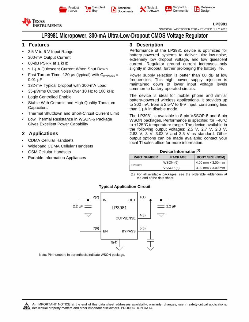
IN
BYPASS
LP39812.2 µF
EN
OUT-SENSE
OUT2(2)
7(6)
1(1)
4(3)
6(5)
5(4)
2.2 µF
Product
Folder
Sample &Buy
Technical
Documents
Tools &
Software
Support &Community
ReferenceDesign
LP3981SNVS159H –OCTOBER 2001–REVISED JULY 2015
LP3981 Micropower, 300-mA Ultra-Low-Dropout CMOS Voltage Regulator1 Features 3 Description
Performance of the LP3981 device is optimized for1• 2.5-V to 6-V Input Range
battery-powered systems to deliver ultra-low-noise,• 300-mA Output Current extremely low dropout voltage, and low quiescent• 60-dB PSRR at 1 kHz current. Regulator ground current increases only
slightly in dropout, further prolonging the battery life.• ≤ 1-μA Quiescent Current When Shut Down• Fast Turnon Time: 120 μs (typical) with CBYPASS = Power supply rejection is better than 60 dB at low
0.01 µF frequencies. This high power supply rejection ismaintained down to lower input voltage levels• 132-mV Typical Dropout with 300-mA Loadcommon to battery-operated circuits.• 35-μVrms Output Noise Over 10 Hz to 100 kHzThe device is ideal for mobile phone and similar• Logic Controlled Enablebattery-powered wireless applications. It provides up
• Stable With Ceramic and High-Quality Tantalum to 300 mA, from a 2.5-V to 6-V input, consuming lessCapacitors than 1 µA in disable mode.
• Thermal Shutdown and Short-Circuit Current Limit The LP3981 is available in 8-pin VSSOP-8 and 6-pin• Low Thermal Resistance in WSON-6 Package WSON packages. Performance is specified for −40°C
Gives Excellent Power Capability to +125°C temperature range. The device available inthe following output voltages: 2.5 V, 2.7 V, 2.8 V,2.83 V, 3 V, 3.03 V and 3.3 V as standard. Other2 Applicationsoutput options can be made available; contact your• CDMA Cellular Handsets local TI sales office for more information.
• Wideband CDMA Cellular HandsetsDevice Information(1)• GSM Cellular Handsets
PART NUMBER PACKAGE BODY SIZE (NOM)• Portable Information AppliancesWSON (6) 4.00 mm x 3.00 mm
LP3981VSSOP (8) 3.00 mm x 3.00 mm
(1) For all available packages, see the orderable addendum atthe end of the data sheet.
Typical Application Circuit
Note: Pin numbers in parenthesis indicate WSON package.
1
An IMPORTANT NOTICE at the end of this data sheet addresses availability, warranty, changes, use in safety-critical applications,intellectual property matters and other important disclaimers. PRODUCTION DATA.
LP3981SNVS159H –OCTOBER 2001–REVISED JULY 2015 www.ti.com
Table of Contents8.2 Functional Block Diagram ....................................... 101 Features .................................................................. 18.3 Feature Description................................................. 102 Applications ........................................................... 18.4 Device Functional Modes........................................ 113 Description ............................................................. 1
9 Application and Implementation ........................ 124 Revision History..................................................... 29.1 Application Information............................................ 125 Pin Configuration and Functions ......................... 39.2 Typical Application ................................................. 126 Specifications......................................................... 4
10 Power Supply Recommendations ..................... 156.1 Absolute Maximum Ratings ...................................... 411 Layout................................................................... 156.2 ESD Ratings.............................................................. 4
11.1 Layout Guidelines ................................................. 156.3 Recommended Operating Conditions....................... 411.2 Layout Example .................................................... 156.4 Thermal Information .................................................. 4
12 Device and Documentation Support ................. 166.5 Electrical Characteristics........................................... 512.1 Community Resources.......................................... 166.6 Timing Requirements ................................................ 612.2 Trademarks ........................................................... 166.7 Typical Characteristics .............................................. 712.3 Electrostatic Discharge Caution............................ 167 Parameter Measurement Information .................. 912.4 Glossary ................................................................ 168 Detailed Description ............................................ 10
13 Mechanical, Packaging, and Orderable8.1 Overview ................................................................. 10Information ........................................................... 16
4 Revision HistoryNOTE: Page numbers for previous revisions may differ from page numbers in the current version.
Changes from Revision G (May 2013) to Revision H Page
• Added Device Information and Pin Configuration and Functions sections, ESD Rating table, Feature Description,Device Functional Modes, Application and Implementation, Power Supply Recommendations, Layout, Device andDocumentation Support , and Mechanical, Packaging, and Orderable Information sections ................................................ 1
• Update pin names to TI nomenclature .................................................................................................................................. 1• Deleted Ordering Information table - duplicative of POA ....................................................................................................... 1• Deleted Lead temperature spec from Abs Max table - it is in POA. ..................................................................................... 4• Deleted rows for max power dissipation - info in Power Dissipation and Device Operation ................................................. 4• Deleted rows for max power dissipation - info in Power Dissipation and Device Operation ................................................. 4• Added 2 new paragraphs to Power Dissipation and Device Operation subsection. ............................................................ 13
Changes from Revision F (May 2013) to Revision G Page
• Changed layout of National Data Sheet to TI format ........................................................................................................... 10
2 Submit Documentation Feedback Copyright © 2001–2015, Texas Instruments Incorporated
Product Folder Links: LP3981
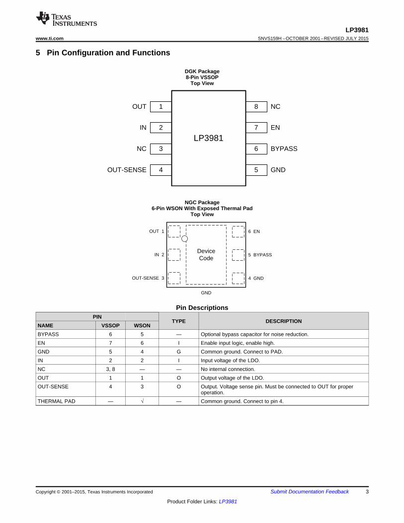
DeviceCode
IN 2
GND
6 ENOUT 1
4 GNDOUT-SENSE 3
5 BYPASS
NC
OUT-SENSE
OUT
LP3981
1
2
3
4 5
6
7
8
IN
NC
EN
BYPASS
GND
LP3981www.ti.com SNVS159H –OCTOBER 2001–REVISED JULY 2015
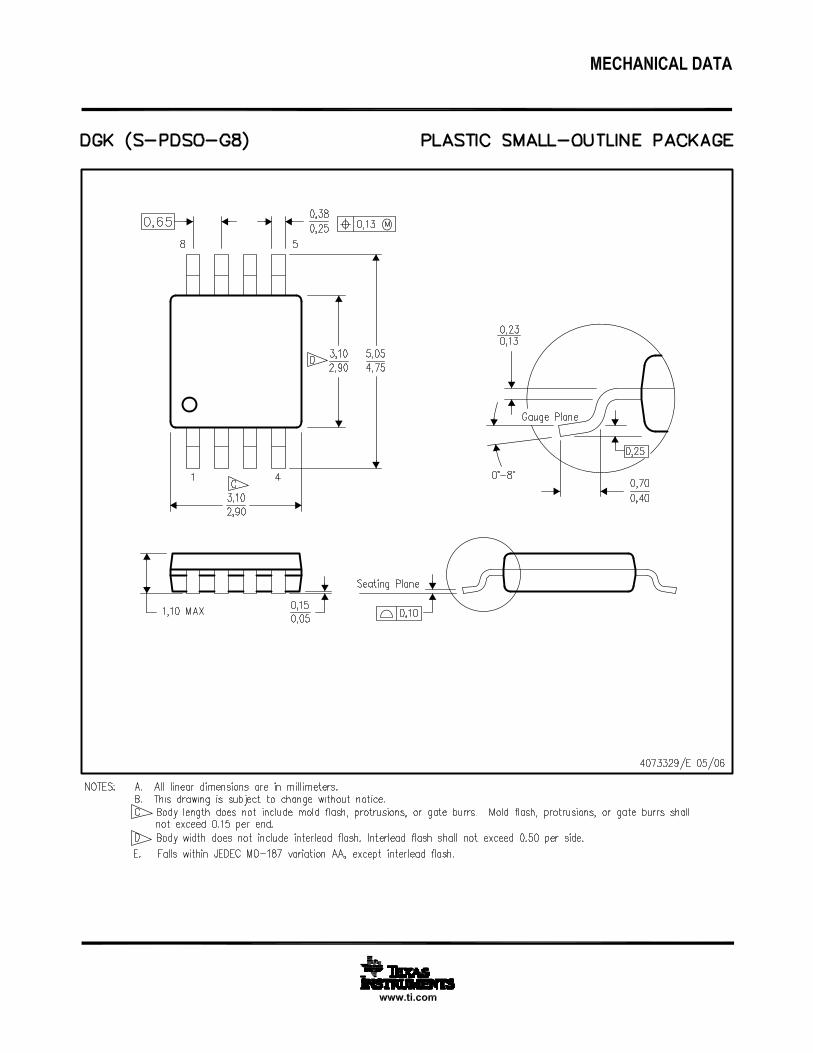
5 Pin Configuration and Functions
DGK Package8-Pin VSSOP
Top View
NGC Package6-Pin WSON With Exposed Thermal Pad
Top View
Pin DescriptionsPIN
TYPE DESCRIPTIONNAME VSSOP WSONBYPASS 6 5 — Optional bypass capacitor for noise reduction.EN 7 6 I Enable input logic, enable high.GND 5 4 G Common ground. Connect to PAD.IN 2 2 I Input voltage of the LDO.NC 3, 8 — — No internal connection.OUT 1 1 O Output voltage of the LDO.OUT-SENSE 4 3 O Output. Voltage sense pin. Must be connected to OUT for proper
operation.THERMAL PAD — √ — Common ground. Connect to pin 4.
Copyright © 2001–2015, Texas Instruments Incorporated Submit Documentation Feedback 3
Product Folder Links: LP3981
LP3981SNVS159H –OCTOBER 2001–REVISED JULY 2015 www.ti.com
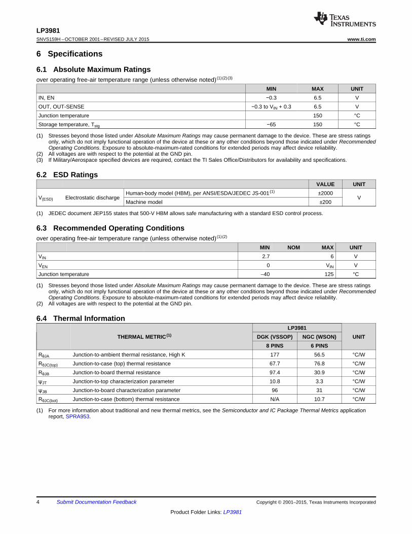
6 Specifications
6.1 Absolute Maximum Ratingsover operating free-air temperature range (unless otherwise noted) (1) (2) (3)
MIN MAX UNITIN, EN −0.3 6.5 VOUT, OUT-SENSE −0.3 to VIN + 0.3 6.5 VJunction temperature 150 °CStorage temperature, Tstg −65 150 °C
(1) Stresses beyond those listed under Absolute Maximum Ratings may cause permanent damage to the device. These are stress ratingsonly, which do not imply functional operation of the device at these or any other conditions beyond those indicated under RecommendedOperating Conditions. Exposure to absolute-maximum-rated conditions for extended periods may affect device reliability.
(2) All voltages are with respect to the potential at the GND pin.(3) If Military/Aerospace specified devices are required, contact the TI Sales Office/Distributors for availability and specifications.
6.2 ESD RatingsVALUE UNIT
Human-body model (HBM), per ANSI/ESDA/JEDEC JS-001 (1) ±2000V(ESD) Electrostatic discharge V
Machine model ±200
(1) JEDEC document JEP155 states that 500-V HBM allows safe manufacturing with a standard ESD control process.
6.3 Recommended Operating Conditionsover operating free-air temperature range (unless otherwise noted) (1) (2)
MIN NOM MAX UNITVIN 2.7 6 VVEN 0 VIN VJunction temperature –40 125 °C
(1) Stresses beyond those listed under Absolute Maximum Ratings may cause permanent damage to the device. These are stress ratingsonly, which do not imply functional operation of the device at these or any other conditions beyond those indicated under RecommendedOperating Conditions. Exposure to absolute-maximum-rated conditions for extended periods may affect device reliability.
(2) All voltages are with respect to the potential at the GND pin.
6.4 Thermal InformationLP3981
THERMAL METRIC (1) DGK (VSSOP) NGC (WSON) UNIT8 PINS 6 PINS
RθJA Junction-to-ambient thermal resistance, High K 177 56.5 °C/WRθJC(top) Junction-to-case (top) thermal resistance 67.7 76.8 °C/WRθJB Junction-to-board thermal resistance 97.4 30.9 °C/WψJT Junction-to-top characterization parameter 10.8 3.3 °C/WψJB Junction-to-board characterization parameter 96 31 °C/WRθJC(bot) Junction-to-case (bottom) thermal resistance N/A 10.7 °C/W
(1) For more information about traditional and new thermal metrics, see the Semiconductor and IC Package Thermal Metrics applicationreport, SPRA953.
4 Submit Documentation Feedback Copyright © 2001–2015, Texas Instruments Incorporated
Product Folder Links: LP3981
LP3981www.ti.com SNVS159H –OCTOBER 2001–REVISED JULY 2015
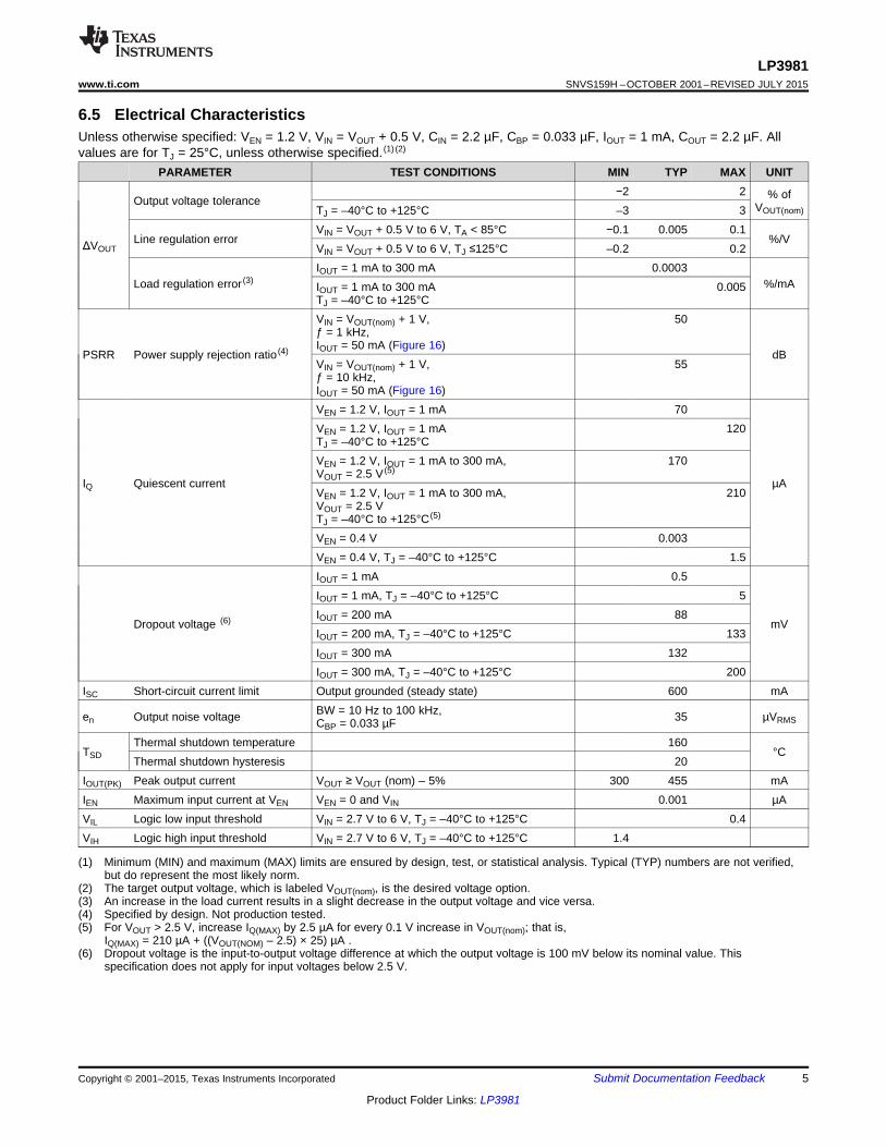
6.5 Electrical CharacteristicsUnless otherwise specified: VEN = 1.2 V, VIN = VOUT + 0.5 V, CIN = 2.2 µF, CBP = 0.033 µF, IOUT = 1 mA, COUT = 2.2 µF. Allvalues are for TJ = 25°C, unless otherwise specified. (1) (2)
PARAMETER TEST CONDITIONS MIN TYP MAX UNIT−2 2 % ofOutput voltage tolerance VOUT(nom)TJ = –40°C to +125°C –3 3
VIN = VOUT + 0.5 V to 6 V, TA < 85°C −0.1 0.005 0.1Line regulation error %/VΔVOUT VIN = VOUT + 0.5 V to 6 V, TJ ≤125°C –0.2 0.2
IOUT = 1 mA to 300 mA 0.0003Load regulation error (3) %/mAIOUT = 1 mA to 300 mA 0.005
TJ = –40°C to +125°CVIN = VOUT(nom) + 1 V, 50ƒ = 1 kHz,IOUT = 50 mA (Figure 16)
PSRR Power supply rejection ratio (4) dBVIN = VOUT(nom) + 1 V, 55ƒ = 10 kHz,IOUT = 50 mA (Figure 16)VEN = 1.2 V, IOUT = 1 mA 70VEN = 1.2 V, IOUT = 1 mA 120TJ = –40°C to +125°CVEN = 1.2 V, IOUT = 1 mA to 300 mA, 170VOUT = 2.5 V (5)
IQ Quiescent current µAVEN = 1.2 V, IOUT = 1 mA to 300 mA, 210VOUT = 2.5 VTJ = –40°C to +125°C (5)
VEN = 0.4 V 0.003VEN = 0.4 V, TJ = –40°C to +125°C 1.5IOUT = 1 mA 0.5IOUT = 1 mA, TJ = –40°C to +125°C 5IOUT = 200 mA 88
Dropout voltage (6) mVIOUT = 200 mA, TJ = –40°C to +125°C 133IOUT = 300 mA 132IOUT = 300 mA, TJ = –40°C to +125°C 200
ISC Short-circuit current limit Output grounded (steady state) 600 mABW = 10 Hz to 100 kHz,en Output noise voltage 35 µVRMSCBP = 0.033 µF
Thermal shutdown temperature 160TSD °C
Thermal shutdown hysteresis 20IOUT(PK) Peak output current VOUT ≥ VOUT (nom) – 5% 300 455 mAIEN Maximum input current at VEN VEN = 0 and VIN 0.001 µAVIL Logic low input threshold VIN = 2.7 V to 6 V, TJ = –40°C to +125°C 0.4VIH Logic high input threshold VIN = 2.7 V to 6 V, TJ = –40°C to +125°C 1.4
(1) Minimum (MIN) and maximum (MAX) limits are ensured by design, test, or statistical analysis. Typical (TYP) numbers are not verified,but do represent the most likely norm.
(2) The target output voltage, which is labeled VOUT(nom), is the desired voltage option.(3) An increase in the load current results in a slight decrease in the output voltage and vice versa.(4) Specified by design. Not production tested.(5) For VOUT > 2.5 V, increase IQ(MAX) by 2.5 µA for every 0.1 V increase in VOUT(nom); that is,
IQ(MAX) = 210 µA + ((VOUT(NOM) – 2.5) × 25) µA .(6) Dropout voltage is the input-to-output voltage difference at which the output voltage is 100 mV below its nominal value. This
specification does not apply for input voltages below 2.5 V.
Copyright © 2001–2015, Texas Instruments Incorporated Submit Documentation Feedback 5
Product Folder Links: LP3981
LP3981SNVS159H –OCTOBER 2001–REVISED JULY 2015 www.ti.com
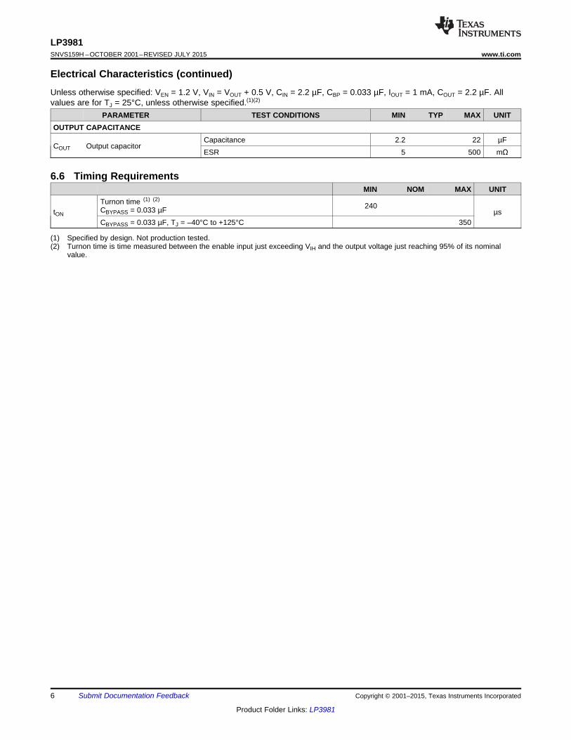
Electrical Characteristics (continued)Unless otherwise specified: VEN = 1.2 V, VIN = VOUT + 0.5 V, CIN = 2.2 µF, CBP = 0.033 µF, IOUT = 1 mA, COUT = 2.2 µF. Allvalues are for TJ = 25°C, unless otherwise specified.(1)(2)
PARAMETER TEST CONDITIONS MIN TYP MAX UNITOUTPUT CAPACITANCE
Capacitance 2.2 22 µFCOUT Output capacitor
ESR 5 500 mΩ
6.6 Timing RequirementsMIN NOM MAX UNIT
Turnon time (1) (2)240CBYPASS = 0.033 µFtON µs
CBYPASS = 0.033 µF, TJ = –40°C to +125°C 350
(1) Specified by design. Not production tested.(2) Turnon time is time measured between the enable input just exceeding VIH and the output voltage just reaching 95% of its nominal
value.
6 Submit Documentation Feedback Copyright © 2001–2015, Texas Instruments Incorporated
Product Folder Links: LP3981
LP3981www.ti.com SNVS159H –OCTOBER 2001–REVISED JULY 2015
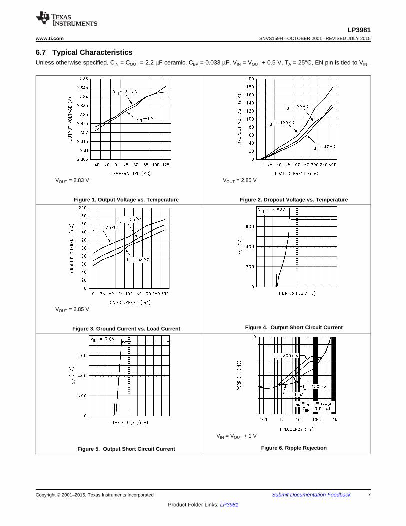
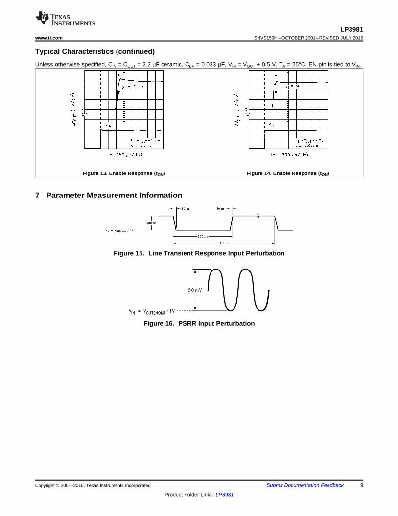
6.7 Typical CharacteristicsUnless otherwise specified, CIN = COUT = 2.2 µF ceramic, CBP = 0.033 µF, VIN = VOUT + 0.5 V, TA = 25°C, EN pin is tied to VIN.
VOUT = 2.83 V VOUT = 2.85 V
Figure 1. Output Voltage vs. Temperature Figure 2. Dropout Voltage vs. Temperature
VOUT = 2.85 V
Figure 4. Output Short Circuit CurrentFigure 3. Ground Current vs. Load Current
VIN = VOUT + 1 V
Figure 6. Ripple RejectionFigure 5. Output Short Circuit Current
Copyright © 2001–2015, Texas Instruments Incorporated Submit Documentation Feedback 7
Product Folder Links: LP3981
LP3981SNVS159H –OCTOBER 2001–REVISED JULY 2015 www.ti.com
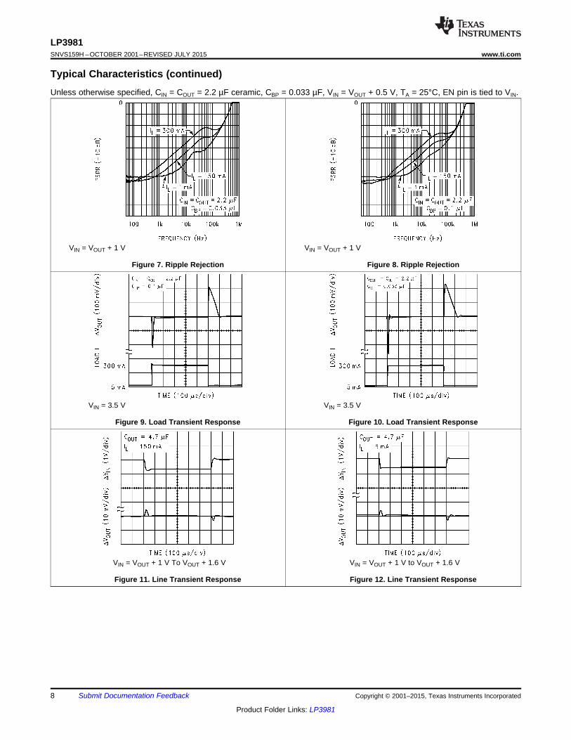
Typical Characteristics (continued)Unless otherwise specified, CIN = COUT = 2.2 µF ceramic, CBP = 0.033 µF, VIN = VOUT + 0.5 V, TA = 25°C, EN pin is tied to VIN.
VIN = VOUT + 1 V VIN = VOUT + 1 V
Figure 7. Ripple Rejection Figure 8. Ripple Rejection
VIN = 3.5 V VIN = 3.5 V
Figure 9. Load Transient Response Figure 10. Load Transient Response
VIN = VOUT + 1 V To VOUT + 1.6 V VIN = VOUT + 1 V to VOUT + 1.6 V
Figure 11. Line Transient Response Figure 12. Line Transient Response
8 Submit Documentation Feedback Copyright © 2001–2015, Texas Instruments Incorporated
Product Folder Links: LP3981
LP3981www.ti.com SNVS159H –OCTOBER 2001–REVISED JULY 2015
Typical Characteristics (continued)Unless otherwise specified, CIN = COUT = 2.2 µF ceramic, CBP = 0.033 µF, VIN = VOUT + 0.5 V, TA = 25°C, EN pin is tied to VIN.
Figure 13. Enable Response (tON) Figure 14. Enable Response (tON)
7 Parameter Measurement Information
Figure 15. Line Transient Response Input Perturbation
Figure 16. PSRR Input Perturbation
Copyright © 2001–2015, Texas Instruments Incorporated Submit Documentation Feedback 9
Product Folder Links: LP3981
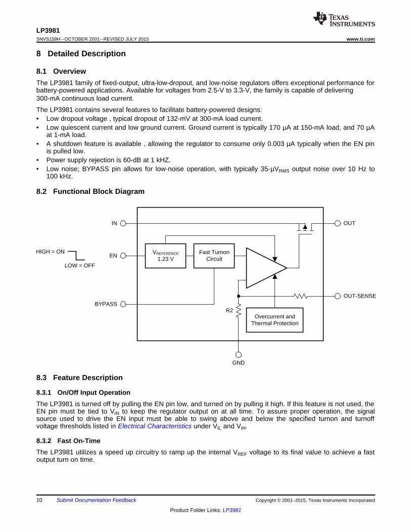
HIGH = ON
LOW = OFF
Overcurrent and Thermal Protection
VREFERENCE
1.23 VFast Turnon
Circuit
R2
IN
EN
BYPASS
OUT
OUT-SENSE
GND
LP3981SNVS159H –OCTOBER 2001–REVISED JULY 2015 www.ti.com
8 Detailed Description
8.1 OverviewThe LP3981 family of fixed-output, ultra-low-dropout, and low-noise regulators offers exceptional performance forbattery-powered applications. Available for voltages from 2.5-V to 3.3-V, the family is capable of delivering300-mA continuous load current.
The LP3981 contains several features to facilitate battery-powered designs:• Low dropout voltage , typical dropout of 132-mV at 300-mA load current.• Low quiescent current and low ground current. Ground current is typically 170 µA at 150-mA load, and 70 µA
at 1-mA load.• A shutdown feature is available , allowing the regulator to consume only 0.003 µA typically when the EN pin
is pulled low.• Power supply rejection is 60-dB at 1 kHZ.• Low noise; BYPASS pin allows for low-noise operation, with typically 35-µVRMS output noise over 10 Hz to
100 kHz.
8.2 Functional Block Diagram
8.3 Feature Description
8.3.1 On/Off Input OperationThe LP3981 is turned off by pulling the EN pin low, and turned on by pulling it high. If this feature is not used, theEN pin must be tied to VIN to keep the regulator output on at all time. To assure proper operation, the signalsource used to drive the EN input must be able to swing above and below the specified turnon and turnoffvoltage thresholds listed in Electrical Characteristics under VIL and VIH.
8.3.2 Fast On-TimeThe LP3981 utilizes a speed up circuitry to ramp up the internal VREF voltage to its final value to achieve a fastoutput turn on time.
10 Submit Documentation Feedback Copyright © 2001–2015, Texas Instruments Incorporated
Product Folder Links: LP3981
LP3981www.ti.com SNVS159H –OCTOBER 2001–REVISED JULY 2015
8.4 Device Functional Modes
8.4.1 Operation with VOUT(TARGET) + 0.3 V ≤ VIN ≤ 6 VThe device operate if the input voltage is equal to, or exceeds VOUT(TARGET) + 0.3 V. At input voltages below theminimum VIN requirement, the devices do not operate correctly and output voltage may not reach target value.
8.4.2 Operation With EN ControlIf the voltage on the EN pin is less than 0.4 V, the device is disabled, and in this state the shutdown current doesnot exceed 1.5 μA. Raising EN above 1.4 V initiates the start-up sequence of the device.
Copyright © 2001–2015, Texas Instruments Incorporated Submit Documentation Feedback 11
Product Folder Links: LP3981
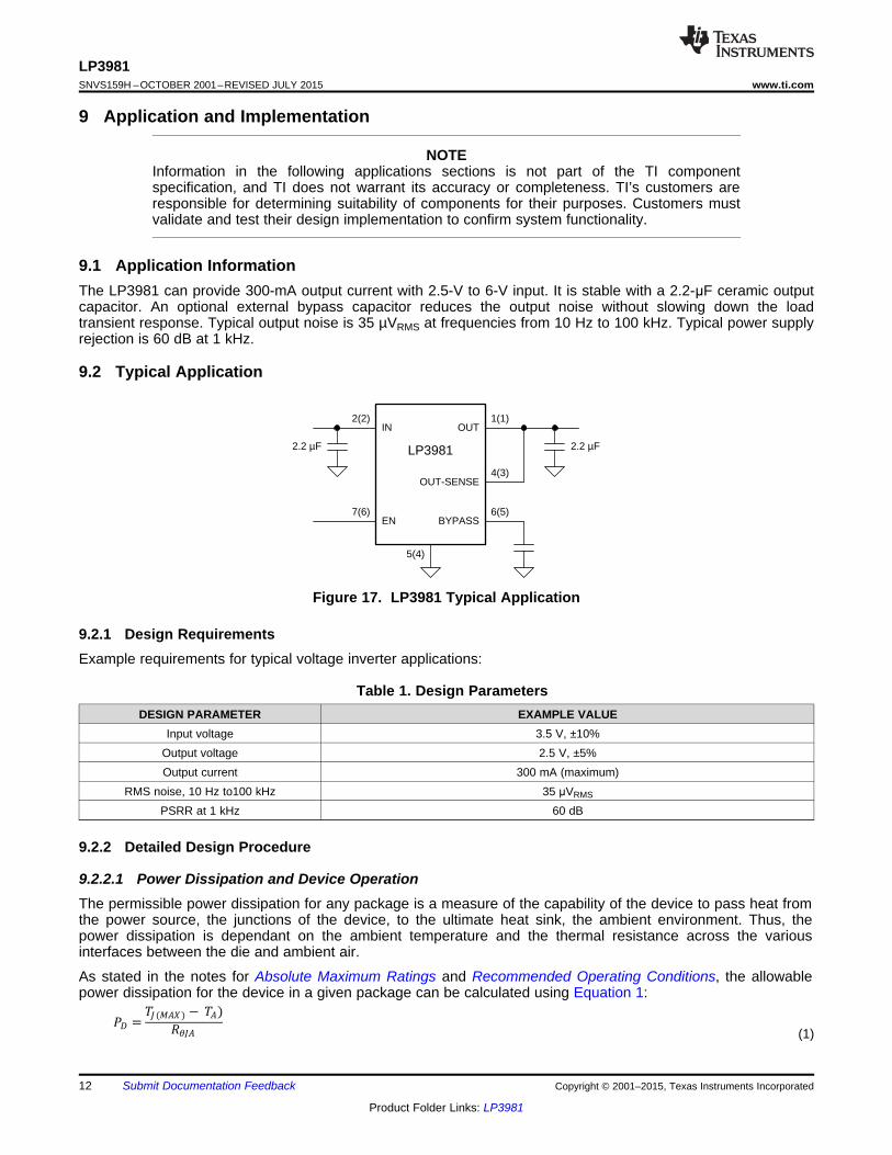
2& =6,(/#:) F 6#)
4à,#
IN
BYPASS
LP39812.2 µF
EN
OUT-SENSE
OUT2(2)
7(6)
1(1)
4(3)
6(5)
5(4)
2.2 µF
LP3981SNVS159H –OCTOBER 2001–REVISED JULY 2015 www.ti.com
9 Application and Implementation
NOTEInformation in the following applications sections is not part of the TI componentspecification, and TI does not warrant its accuracy or completeness. TI’s customers areresponsible for determining suitability of components for their purposes. Customers mustvalidate and test their design implementation to confirm system functionality.
9.1 Application InformationThe LP3981 can provide 300-mA output current with 2.5-V to 6-V input. It is stable with a 2.2-μF ceramic outputcapacitor. An optional external bypass capacitor reduces the output noise without slowing down the loadtransient response. Typical output noise is 35 µVRMS at frequencies from 10 Hz to 100 kHz. Typical power supplyrejection is 60 dB at 1 kHz.
9.2 Typical Application
Figure 17. LP3981 Typical Application
9.2.1 Design RequirementsExample requirements for typical voltage inverter applications:
Table 1. Design ParametersDESIGN PARAMETER EXAMPLE VALUE
Input voltage 3.5 V, ±10%Output voltage 2.5 V, ±5%Output current 300 mA (maximum)
RMS noise, 10 Hz to100 kHz 35 μVRMS
PSRR at 1 kHz 60 dB
9.2.2 Detailed Design Procedure
9.2.2.1 Power Dissipation and Device OperationThe permissible power dissipation for any package is a measure of the capability of the device to pass heat fromthe power source, the junctions of the device, to the ultimate heat sink, the ambient environment. Thus, thepower dissipation is dependant on the ambient temperature and the thermal resistance across the variousinterfaces between the die and ambient air.
As stated in the notes for Absolute Maximum Ratings and Recommended Operating Conditions, the allowablepower dissipation for the device in a given package can be calculated using Equation 1:
(1)
12 Submit Documentation Feedback Copyright © 2001–2015, Texas Instruments Incorporated
Product Folder Links: LP3981
2& = :8+0 F 8176; × +176
LP3981www.ti.com SNVS159H –OCTOBER 2001–REVISED JULY 2015
With an RθJA = 56.5°C/W, the device in the WSON package returns a value of 1.77 W with a maximum junctiontemperature of 125°C and an ambient temperature of 25°C. The device in a VSSOP package returns a figure of0.565 W (R θJA = 177°C/W).
The actual power dissipation across the device can be represented by Equation 2:(2)
This establishes the relationship between the power dissipation allowed due to thermal considerations, thevoltage drop across the device, and the continuous current capability of the device. The device can deliver 300mA but care must be taken when choosing the continuous current output for the device under the operating loadconditions.
The RθJA value is not a characteristic of the package by itself but of the package, the printed circuit board(PCB), and other environmental factors. Equation 2 is only valid when the application configuration matches theEIA/JEDEC JESD51-7 (High-K) configuration in which RθJA was either measured or modeled. Few, if any, userapplications conform to the PCB configuration defined by the EIA/JEDEC standards. As a result, the RθJA valuesare useful only when comparing assorted packages that have been measured or modeled to the EIA/JEDECstandards, but are of little use to estimate real world junction temperatures.
The EIA/JEDEC standard JESD51-2 provides methodologies to estimate the junction temperature from externalmeasurements (ψJB references the temperature at the PCB, and ψJT references the temperature at the topsurface of the package) when operating under steady-state power dissipation conditions. These methodologieshave been determined to be relatively independent of the PCB attached to the package when compared to themore typical RθJA. Refer to Semiconductor and IC Package Thermal Metrics application report, SPRA953, forspecifics.
9.2.2.2 External CapacitorsLike any low-dropout regulator, the LP3981 requires external capacitors for regulator stability. The LP3981 isspecifically designed for portable applications requiring minimum board space and smallest components. Thesecapacitors must be correctly selected for good performance.
9.2.2.3 Input CapacitorAn input capacitance of ≊ 2.2 µF is required between the LP3981 input pin and ground (the amount of thecapacitance may be increased without limit).
This capacitor must be located a distance of not more than 1 cm from the input pin and returned to a cleananalog ground. Any good quality ceramic, tantalum, or film capacitor may be used at the input.
NOTETantalum capacitors can suffer catastrophic failures due to surge current when connectedto a low-impedance source of power (like a battery or a very large capacitor). If a tantalumcapacitor is used at the input, it must be specified by the manufacturer to have a surgecurrent rating sufficient for the application.
There are no requirements for the ESR on the input capacitor, but tolerance and temperature coefficient must beconsidered when selecting the capacitor to ensure the capacitance is ≊ 2.2 µF over the entire operatingtemperature range.
9.2.2.4 Output CapacitorThe LP3981 is designed specifically to work with very small ceramic output capacitors. A ceramic capacitor(dielectric types Z5U, Y5V or X7R) in the 2.2-µF to 22-µF range with 5-mΩ to 500-mΩ ESR is suitable in theLP3981 application circuit.
It is also possible to use tantalum or film capacitors at the output, but these are not as attractive for reasons ofsize and cost (see Capacitor Characteristics).
The output capacitor must meet the requirement for minimum amount of capacitance and also have anequivalent series resistance (ESR) value which is within a stable range (5 mΩ to 500 mΩ).
Copyright © 2001–2015, Texas Instruments Incorporated Submit Documentation Feedback 13
Product Folder Links: LP3981
LP3981SNVS159H –OCTOBER 2001–REVISED JULY 2015 www.ti.com
9.2.2.5 No-Load StabilityThe LP3981 remains stable and in regulation with no external load. This is specially important in CMOS RAMkeep-alive applications.
9.2.2.6 Noise Bypass CapacitorConnecting a 0.033-µF capacitor between the BYPASS pin and ground significantly reduces noise on theregulator output. This capacitor is connected directly to a high impedance node in the bad gap reference circuit.Any significant loading on this node causes a change on the regulated output voltage. For this reason, DCleakage current through this pin must be kept as low as possible for best output voltage accuracy.
The types of capacitors best suited for the noise bypass capacitor are ceramic and film. Hight-quality ceramiccapacitors with either NPO or COG dielectric typically have very low leakage. Polypropolene and polycarbonatefilm capacitors are available in small surface-mount packages and typically have extremely low leakage current.
Unlike many other LDOs, addition of a noise reduction capacitor does not effect the transient response of thedevice.
9.2.2.7 Capacitor CharacteristicsThe LP3981 is designed to work with ceramic capacitors on the output to take advantage of the benefits theyoffer: for capacitance values in the range of 1 µF to 4.7 µF, ceramic capacitors are the smallest, least expensiveand have the lowest ESR values (which makes them best for eliminating high frequency noise). The ESR of atypical 1µF ceramic capacitor is in the range of 20 mΩ to 40 mΩ, which easily meets the ESR requirement forstability by the LP3981.
Capacitance of a ceramic capacitor can vary with temperature. Most large value ceramic capacitors (≊ 2.2 µF)are manufactured with Z5U or Y5V temperature characteristics, which results in the capacitance dropping bymore than 50% as the temperature goes from 25°C to 85°C.
A better choice for temperature coefficient in a ceramic capacitor is X7R, which holds the capacitance within±15%.
Tantalum capacitors are less desirable than ceramic for use as output capacitors because they are moreexpensive when comparing equivalent capacitance and voltage ratings in the 1-µF to 4.7-µF range.
Another important consideration is that tantalum capacitors have higher ESR values than equivalently sizedceramics. This means that while it may be possible to find a tantalum capacitor with an ESR value within thestable range, it would have to be larger in capacitance (which means bigger and more costly) than a ceramiccapacitor with the same ESR value. It must also be noted that the ESR of a typical tantalum increases about 2:1as the temperature goes from 25°C down to −40°C, so some guard band must be allowed.
9.2.3 Application Curves
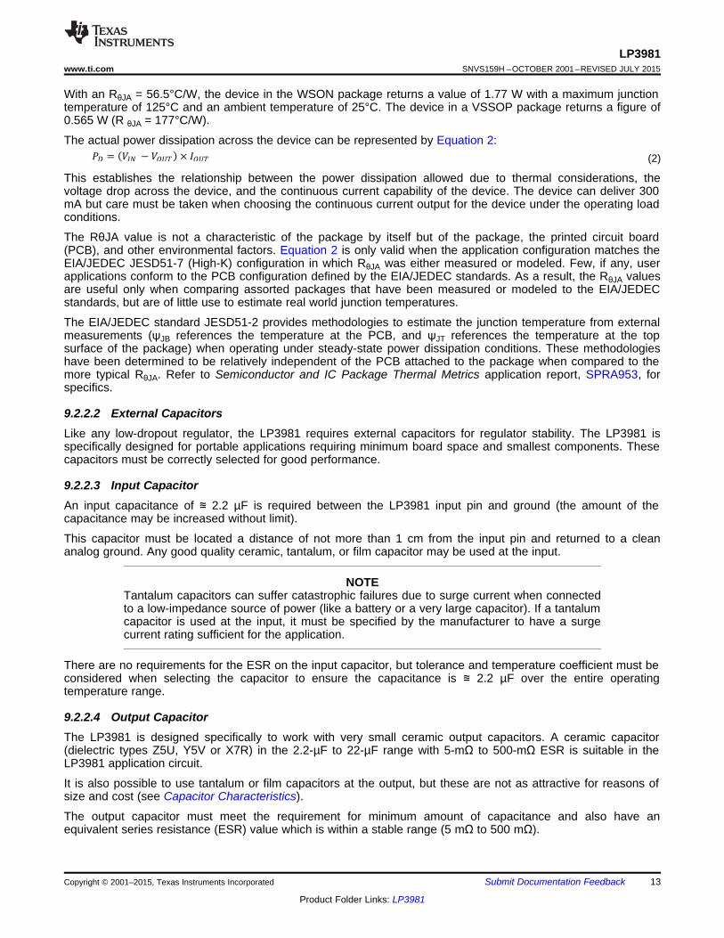
VIN = VOUT + 1 V to VOUT + 1.6 V VIN = VOUT + 1V to VOUT + 1.6 V
Figure 18. Line Transient Response Figure 19. Line Transient Response
14 Submit Documentation Feedback Copyright © 2001–2015, Texas Instruments Incorporated
Product Folder Links: LP3981
1
2
3
6
5
4
OUT
IN
EN
BYPASS
GND
CIN
COUT
CBYPASS
OUT-SENSE
LP3981www.ti.com SNVS159H –OCTOBER 2001–REVISED JULY 2015
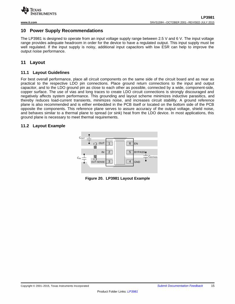
10 Power Supply RecommendationsThe LP3981 is designed to operate from an input voltage supply range between 2.5 V and 6 V. The input voltagerange provides adequate headroom in order for the device to have a regulated output. This input supply must bewell regulated. If the input supply is noisy, additional input capacitors with low ESR can help to improve theoutput noise performance.
11 Layout
11.1 Layout GuidelinesFor best overall performance, place all circuit components on the same side of the circuit board and as near aspractical to the respective LDO pin connections. Place ground return connections to the input and outputcapacitor, and to the LDO ground pin as close to each other as possible, connected by a wide, component-side,copper surface. The use of vias and long traces to create LDO circuit connections is strongly discouraged andnegatively affects system performance. This grounding and layout scheme minimizes inductive parasitics, andthereby reduces load-current transients, minimizes noise, and increases circuit stability. A ground referenceplane is also recommended and is either embedded in the PCB itself or located on the bottom side of the PCBopposite the components. This reference plane serves to assure accuracy of the output voltage, shield noise,and behaves similar to a thermal plane to spread (or sink) heat from the LDO device. In most applications, thisground plane is necessary to meet thermal requirements.
11.2 Layout Example
Figure 20. LP3981 Layout Example
Copyright © 2001–2015, Texas Instruments Incorporated Submit Documentation Feedback 15
Product Folder Links: LP3981
LP3981SNVS159H –OCTOBER 2001–REVISED JULY 2015 www.ti.com
12 Device and Documentation Support
12.1 Community ResourcesThe following links connect to TI community resources. Linked contents are provided "AS IS" by the respectivecontributors. They do not constitute TI specifications and do not necessarily reflect TI's views; see TI's Terms ofUse.
TI E2E™ Online Community TI's Engineer-to-Engineer (E2E) Community. Created to foster collaborationamong engineers. At e2e.ti.com, you can ask questions, share knowledge, explore ideas and helpsolve problems with fellow engineers.
Design Support TI's Design Support Quickly find helpful E2E forums along with design support tools andcontact information for technical support.
12.2 TrademarksE2E is a trademark of Texas Instruments.All other trademarks are the property of their respective owners.
12.3 Electrostatic Discharge CautionThese devices have limited built-in ESD protection. The leads should be shorted together or the device placed in conductive foamduring storage or handling to prevent electrostatic damage to the MOS gates.
12.4 GlossarySLYZ022 — TI Glossary.
This glossary lists and explains terms, acronyms, and definitions.
13 Mechanical, Packaging, and Orderable InformationThe following pages include mechanical, packaging, and orderable information. This information is the mostcurrent data available for the designated devices. This data is subject to change without notice and revision ofthis document. For browser-based versions of this data sheet, refer to the left-hand navigation.
16 Submit Documentation Feedback Copyright © 2001–2015, Texas Instruments Incorporated
Product Folder Links: LP3981
PACKAGE OPTION ADDENDUM
www.ti.com 14-Sep-2018
Addendum-Page 1
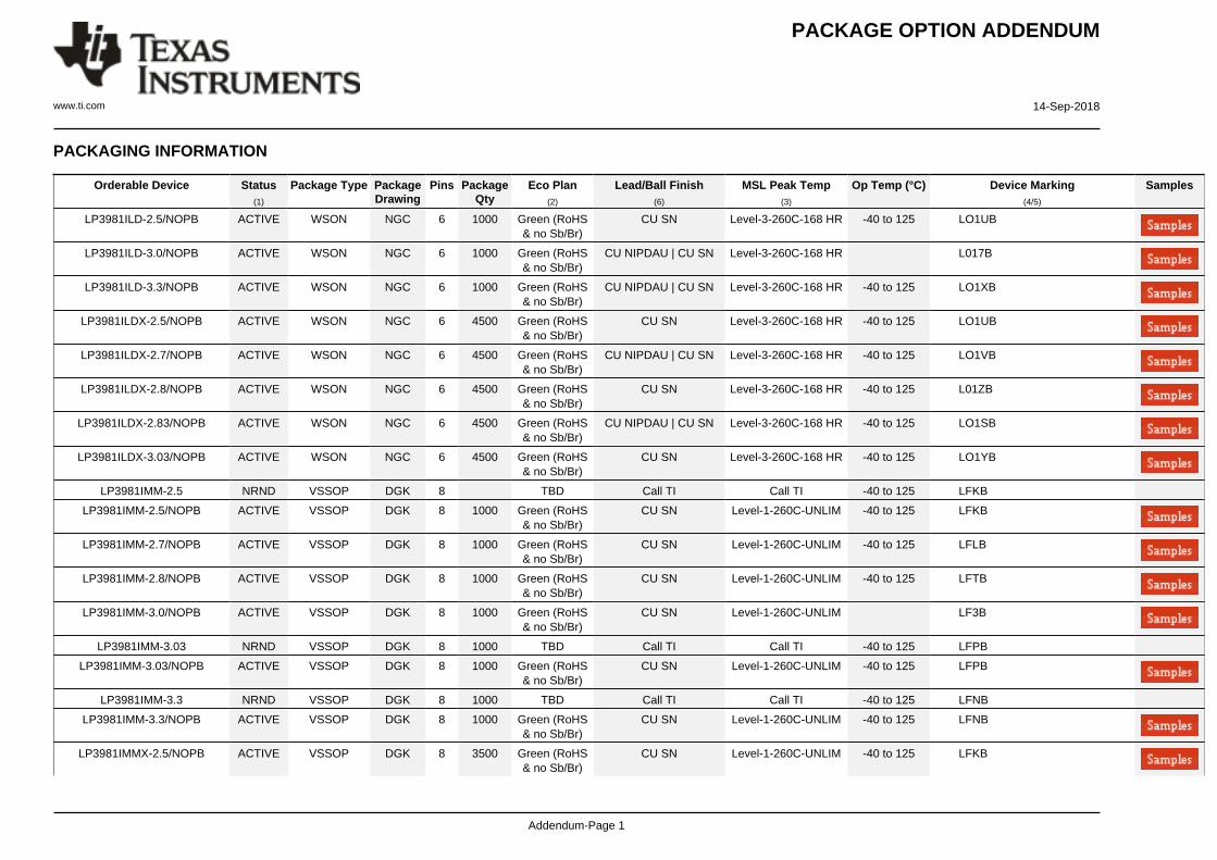
PACKAGING INFORMATION
Orderable Device Status(1)
Package Type PackageDrawing
Pins PackageQty
Eco Plan(2)
Lead/Ball Finish(6)
MSL Peak Temp(3)
Op Temp (°C) Device Marking(4/5)
Samples
LP3981ILD-2.5/NOPB ACTIVE WSON NGC 6 1000 Green (RoHS& no Sb/Br)
CU SN Level-3-260C-168 HR -40 to 125 LO1UB
LP3981ILD-3.0/NOPB ACTIVE WSON NGC 6 1000 Green (RoHS& no Sb/Br)
CU NIPDAU | CU SN Level-3-260C-168 HR L017B
LP3981ILD-3.3/NOPB ACTIVE WSON NGC 6 1000 Green (RoHS& no Sb/Br)
CU NIPDAU | CU SN Level-3-260C-168 HR -40 to 125 LO1XB
LP3981ILDX-2.5/NOPB ACTIVE WSON NGC 6 4500 Green (RoHS& no Sb/Br)
CU SN Level-3-260C-168 HR -40 to 125 LO1UB
LP3981ILDX-2.7/NOPB ACTIVE WSON NGC 6 4500 Green (RoHS& no Sb/Br)
CU NIPDAU | CU SN Level-3-260C-168 HR -40 to 125 LO1VB
LP3981ILDX-2.8/NOPB ACTIVE WSON NGC 6 4500 Green (RoHS& no Sb/Br)
CU SN Level-3-260C-168 HR -40 to 125 L01ZB
LP3981ILDX-2.83/NOPB ACTIVE WSON NGC 6 4500 Green (RoHS& no Sb/Br)
CU NIPDAU | CU SN Level-3-260C-168 HR -40 to 125 LO1SB
LP3981ILDX-3.03/NOPB ACTIVE WSON NGC 6 4500 Green (RoHS& no Sb/Br)
CU SN Level-3-260C-168 HR -40 to 125 LO1YB
LP3981IMM-2.5 NRND VSSOP DGK 8 TBD Call TI Call TI -40 to 125 LFKB
LP3981IMM-2.5/NOPB ACTIVE VSSOP DGK 8 1000 Green (RoHS& no Sb/Br)
CU SN Level-1-260C-UNLIM -40 to 125 LFKB
LP3981IMM-2.7/NOPB ACTIVE VSSOP DGK 8 1000 Green (RoHS& no Sb/Br)
CU SN Level-1-260C-UNLIM -40 to 125 LFLB
LP3981IMM-2.8/NOPB ACTIVE VSSOP DGK 8 1000 Green (RoHS& no Sb/Br)
CU SN Level-1-260C-UNLIM -40 to 125 LFTB
LP3981IMM-3.0/NOPB ACTIVE VSSOP DGK 8 1000 Green (RoHS& no Sb/Br)
CU SN Level-1-260C-UNLIM LF3B
LP3981IMM-3.03 NRND VSSOP DGK 8 1000 TBD Call TI Call TI -40 to 125 LFPB
LP3981IMM-3.03/NOPB ACTIVE VSSOP DGK 8 1000 Green (RoHS& no Sb/Br)
CU SN Level-1-260C-UNLIM -40 to 125 LFPB
LP3981IMM-3.3 NRND VSSOP DGK 8 1000 TBD Call TI Call TI -40 to 125 LFNB
LP3981IMM-3.3/NOPB ACTIVE VSSOP DGK 8 1000 Green (RoHS& no Sb/Br)
CU SN Level-1-260C-UNLIM -40 to 125 LFNB
LP3981IMMX-2.5/NOPB ACTIVE VSSOP DGK 8 3500 Green (RoHS& no Sb/Br)
CU SN Level-1-260C-UNLIM -40 to 125 LFKB
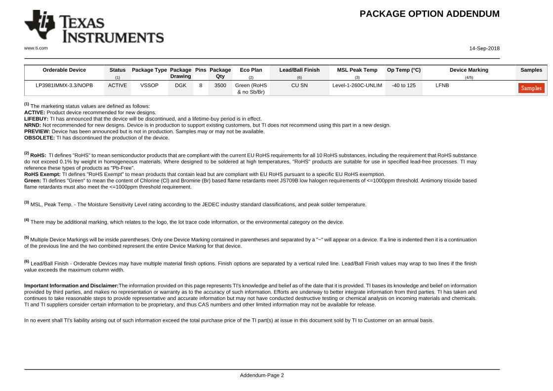
PACKAGE OPTION ADDENDUM
www.ti.com 14-Sep-2018
Addendum-Page 2
Orderable Device Status(1)
Package Type PackageDrawing
Pins PackageQty
Eco Plan(2)
Lead/Ball Finish(6)
MSL Peak Temp(3)
Op Temp (°C) Device Marking(4/5)
Samples
LP3981IMMX-3.3/NOPB ACTIVE VSSOP DGK 8 3500 Green (RoHS& no Sb/Br)
CU SN Level-1-260C-UNLIM -40 to 125 LFNB
(1) The marketing status values are defined as follows:ACTIVE: Product device recommended for new designs.LIFEBUY: TI has announced that the device will be discontinued, and a lifetime-buy period is in effect.NRND: Not recommended for new designs. Device is in production to support existing customers, but TI does not recommend using this part in a new design.PREVIEW: Device has been announced but is not in production. Samples may or may not be available.OBSOLETE: TI has discontinued the production of the device.
(2) RoHS: TI defines "RoHS" to mean semiconductor products that are compliant with the current EU RoHS requirements for all 10 RoHS substances, including the requirement that RoHS substancedo not exceed 0.1% by weight in homogeneous materials. Where designed to be soldered at high temperatures, "RoHS" products are suitable for use in specified lead-free processes. TI mayreference these types of products as "Pb-Free".RoHS Exempt: TI defines "RoHS Exempt" to mean products that contain lead but are compliant with EU RoHS pursuant to a specific EU RoHS exemption.Green: TI defines "Green" to mean the content of Chlorine (Cl) and Bromine (Br) based flame retardants meet JS709B low halogen requirements of <=1000ppm threshold. Antimony trioxide basedflame retardants must also meet the <=1000ppm threshold requirement.
(3) MSL, Peak Temp. - The Moisture Sensitivity Level rating according to the JEDEC industry standard classifications, and peak solder temperature.
(4) There may be additional marking, which relates to the logo, the lot trace code information, or the environmental category on the device.
(5) Multiple Device Markings will be inside parentheses. Only one Device Marking contained in parentheses and separated by a "~" will appear on a device. If a line is indented then it is a continuationof the previous line and the two combined represent the entire Device Marking for that device.
(6) Lead/Ball Finish - Orderable Devices may have multiple material finish options. Finish options are separated by a vertical ruled line. Lead/Ball Finish values may wrap to two lines if the finishvalue exceeds the maximum column width.
Important Information and Disclaimer:The information provided on this page represents TI's knowledge and belief as of the date that it is provided. TI bases its knowledge and belief on informationprovided by third parties, and makes no representation or warranty as to the accuracy of such information. Efforts are underway to better integrate information from third parties. TI has taken andcontinues to take reasonable steps to provide representative and accurate information but may not have conducted destructive testing or chemical analysis on incoming materials and chemicals.TI and TI suppliers consider certain information to be proprietary, and thus CAS numbers and other limited information may not be available for release.
In no event shall TI's liability arising out of such information exceed the total purchase price of the TI part(s) at issue in this document sold by TI to Customer on an annual basis.
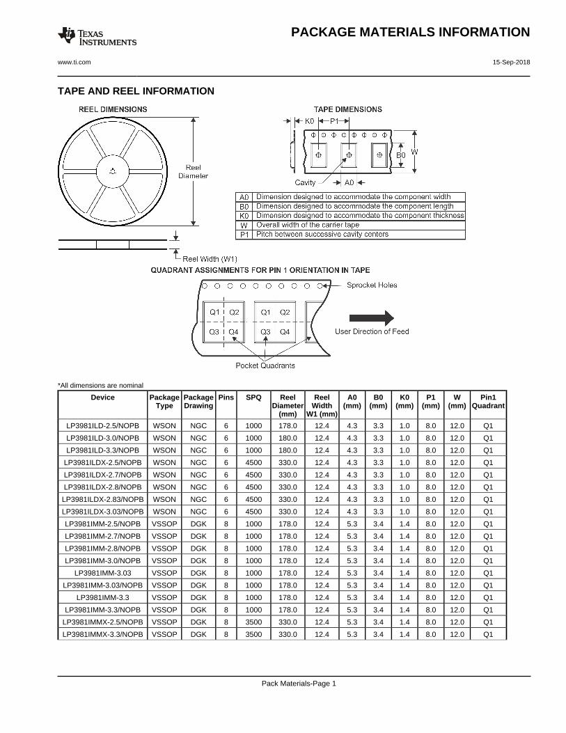
TAPE AND REEL INFORMATION
*All dimensions are nominal
Device PackageType
PackageDrawing
Pins SPQ ReelDiameter
(mm)
ReelWidth
W1 (mm)
A0(mm)
B0(mm)
K0(mm)
P1(mm)
W(mm)
Pin1Quadrant
LP3981ILD-2.5/NOPB WSON NGC 6 1000 178.0 12.4 4.3 3.3 1.0 8.0 12.0 Q1
LP3981ILD-3.0/NOPB WSON NGC 6 1000 180.0 12.4 4.3 3.3 1.0 8.0 12.0 Q1
LP3981ILD-3.3/NOPB WSON NGC 6 1000 180.0 12.4 4.3 3.3 1.0 8.0 12.0 Q1
LP3981ILDX-2.5/NOPB WSON NGC 6 4500 330.0 12.4 4.3 3.3 1.0 8.0 12.0 Q1
LP3981ILDX-2.7/NOPB WSON NGC 6 4500 330.0 12.4 4.3 3.3 1.0 8.0 12.0 Q1
LP3981ILDX-2.8/NOPB WSON NGC 6 4500 330.0 12.4 4.3 3.3 1.0 8.0 12.0 Q1
LP3981ILDX-2.83/NOPB WSON NGC 6 4500 330.0 12.4 4.3 3.3 1.0 8.0 12.0 Q1
LP3981ILDX-3.03/NOPB WSON NGC 6 4500 330.0 12.4 4.3 3.3 1.0 8.0 12.0 Q1
LP3981IMM-2.5/NOPB VSSOP DGK 8 1000 178.0 12.4 5.3 3.4 1.4 8.0 12.0 Q1
LP3981IMM-2.7/NOPB VSSOP DGK 8 1000 178.0 12.4 5.3 3.4 1.4 8.0 12.0 Q1
LP3981IMM-2.8/NOPB VSSOP DGK 8 1000 178.0 12.4 5.3 3.4 1.4 8.0 12.0 Q1
LP3981IMM-3.0/NOPB VSSOP DGK 8 1000 178.0 12.4 5.3 3.4 1.4 8.0 12.0 Q1
LP3981IMM-3.03 VSSOP DGK 8 1000 178.0 12.4 5.3 3.4 1.4 8.0 12.0 Q1
LP3981IMM-3.03/NOPB VSSOP DGK 8 1000 178.0 12.4 5.3 3.4 1.4 8.0 12.0 Q1
LP3981IMM-3.3 VSSOP DGK 8 1000 178.0 12.4 5.3 3.4 1.4 8.0 12.0 Q1
LP3981IMM-3.3/NOPB VSSOP DGK 8 1000 178.0 12.4 5.3 3.4 1.4 8.0 12.0 Q1
LP3981IMMX-2.5/NOPB VSSOP DGK 8 3500 330.0 12.4 5.3 3.4 1.4 8.0 12.0 Q1
LP3981IMMX-3.3/NOPB VSSOP DGK 8 3500 330.0 12.4 5.3 3.4 1.4 8.0 12.0 Q1
PACKAGE MATERIALS INFORMATION
www.ti.com 15-Sep-2018
Pack Materials-Page 1
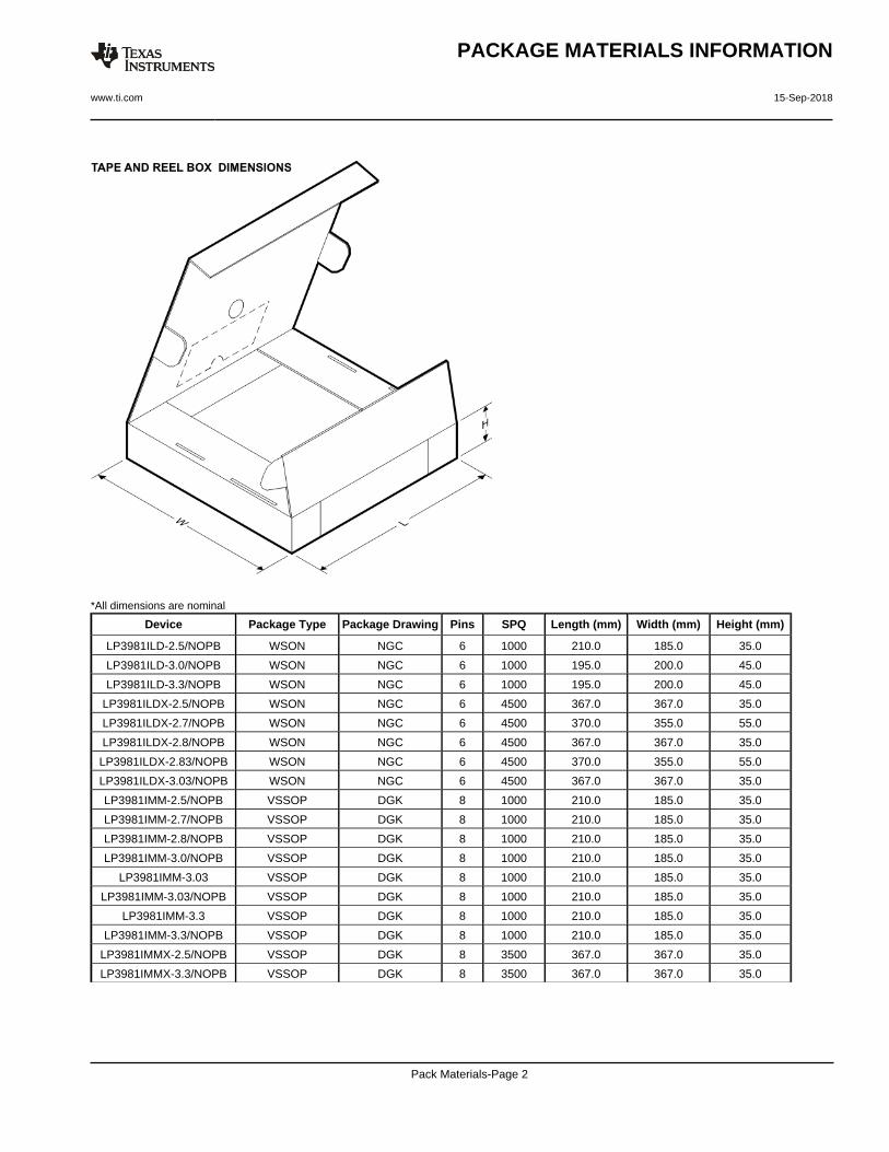
*All dimensions are nominal
Device Package Type Package Drawing Pins SPQ Length (mm) Width (mm) Height (mm)
LP3981ILD-2.5/NOPB WSON NGC 6 1000 210.0 185.0 35.0
LP3981ILD-3.0/NOPB WSON NGC 6 1000 195.0 200.0 45.0
LP3981ILD-3.3/NOPB WSON NGC 6 1000 195.0 200.0 45.0
LP3981ILDX-2.5/NOPB WSON NGC 6 4500 367.0 367.0 35.0
LP3981ILDX-2.7/NOPB WSON NGC 6 4500 370.0 355.0 55.0
LP3981ILDX-2.8/NOPB WSON NGC 6 4500 367.0 367.0 35.0
LP3981ILDX-2.83/NOPB WSON NGC 6 4500 370.0 355.0 55.0
LP3981ILDX-3.03/NOPB WSON NGC 6 4500 367.0 367.0 35.0
LP3981IMM-2.5/NOPB VSSOP DGK 8 1000 210.0 185.0 35.0
LP3981IMM-2.7/NOPB VSSOP DGK 8 1000 210.0 185.0 35.0
LP3981IMM-2.8/NOPB VSSOP DGK 8 1000 210.0 185.0 35.0
LP3981IMM-3.0/NOPB VSSOP DGK 8 1000 210.0 185.0 35.0
LP3981IMM-3.03 VSSOP DGK 8 1000 210.0 185.0 35.0
LP3981IMM-3.03/NOPB VSSOP DGK 8 1000 210.0 185.0 35.0
LP3981IMM-3.3 VSSOP DGK 8 1000 210.0 185.0 35.0
LP3981IMM-3.3/NOPB VSSOP DGK 8 1000 210.0 185.0 35.0
LP3981IMMX-2.5/NOPB VSSOP DGK 8 3500 367.0 367.0 35.0
LP3981IMMX-3.3/NOPB VSSOP DGK 8 3500 367.0 367.0 35.0
PACKAGE MATERIALS INFORMATION
www.ti.com 15-Sep-2018
Pack Materials-Page 2
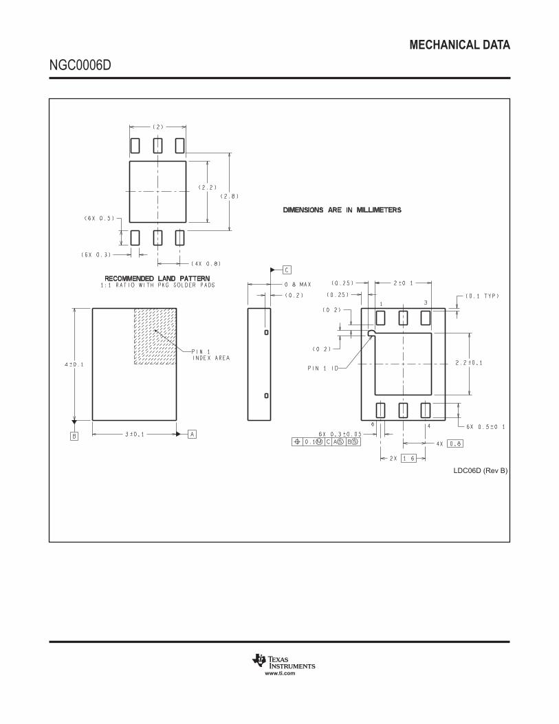
MECHANICAL DATA
NGC0006D
www.ti.com
LDC06D (Rev B)
IMPORTANT NOTICE AND DISCLAIMER
TI PROVIDES TECHNICAL AND RELIABILITY DATA (INCLUDING DATASHEETS), DESIGN RESOURCES (INCLUDING REFERENCEDESIGNS), APPLICATION OR OTHER DESIGN ADVICE, WEB TOOLS, SAFETY INFORMATION, AND OTHER RESOURCES “AS IS”AND WITH ALL FAULTS, AND DISCLAIMS ALL WARRANTIES, EXPRESS AND IMPLIED, INCLUDING WITHOUT LIMITATION ANYIMPLIED WARRANTIES OF MERCHANTABILITY, FITNESS FOR A PARTICULAR PURPOSE OR NON-INFRINGEMENT OF THIRDPARTY INTELLECTUAL PROPERTY RIGHTS.These resources are intended for skilled developers designing with TI products. You are solely responsible for (1) selecting the appropriateTI products for your application, (2) designing, validating and testing your application, and (3) ensuring your application meets applicablestandards, and any other safety, security, or other requirements. These resources are subject to change without notice. TI grants youpermission to use these resources only for development of an application that uses the TI products described in the resource. Otherreproduction and display of these resources is prohibited. No license is granted to any other TI intellectual property right or to any thirdparty intellectual property right. TI disclaims responsibility for, and you will fully indemnify TI and its representatives against, any claims,damages, costs, losses, and liabilities arising out of your use of these resources.TI’s products are provided subject to TI’s Terms of Sale (www.ti.com/legal/termsofsale.html) or other applicable terms available either onti.com or provided in conjunction with such TI products. TI’s provision of these resources does not expand or otherwise alter TI’s applicablewarranties or warranty disclaimers for TI products.
Mailing Address: Texas Instruments, Post Office Box 655303, Dallas, Texas 75265Copyright © 2018, Texas Instruments Incorporated