Embed Size (px)
Citation preview
LPKF-DistributorLPKF Laser & Electronics AGOsteriede 7D-30827 GarbsenGermany
Phone +49(0)5131-7095-0Fax +49(0)5131-7095-90
KF
AG
, 119
838
-10
07-E
N
PRODUCT CATALOG
Circuit Board Plotters
Laser Circuit Structuring
Through-Hole Conductivity
Multilayer Prototyping
SMT/Finishing
Technical Guide
InhouseRapid PCB
Prototyping
www.lpkf.com
PR
OD
UC
T C
ATA
LOG
LPK
F La
ser
& E
lect
roni
cs
Printed circuit board manufacturing – clear and brief
In the workflow overview you will see the simple steps to develop a finished printed circuit board using LPKF technology; process steps for galvanic or chemistry-free through-hole plating are shown. On the declared pages you will find detailed information about the appropriate steps of the production process.
Detailed information starting at page 95.
www.lpkf.com See page 124 to locate an LPKF distributor near you.
Price listsAny price list inserted or attached to this catalog is not a part of this catalog. All prices subject to change. Contact your nearest Distributor for the most current prices.
Technology noteAll specifications are subject to technical modifications.
Privacy policyLPKF protects client and customer personal and professional information. All such submitted information will be used only by LPKF and not resold or shared with any third party.
Indicia
Indicia
129
Phone and FaxPhone +49 (0) 5131-7095-0Fax +49 (0) 5131-7095-90
[email protected]@lpkf.de
LPKF websitewww.lpkf.dewww.lpkf.com
LPKF maintains a worldwide distribution network. Find the most convenient one on page 124, or visit www.lpkf.com for more information.
Here you find all information you need. Our competent sales and service team is waiting for your call.
Placing an order? Need technical support? No problem!
Europe (LPKF Headquarters)
North/Central America China
LPKF Sales and Service
Worldwide LPKF distribution partners
Phone and Fax Phone +1 (503) 454-4219Fax +1 (503) 682-7151
[email protected]@lpkfusa.com
LPKF websitewww.lpkfusa.com
Phone and Fax Sales Phone +86-13920308369Service Phone +86-13032289111Fax +86-2223006965
LPKF websitewww.lpkf.cn
Indicia, trademarks, and patents© 2007 LPKF Laser & Electronics AG, Garbsen, Germany. All rights reserved. Systems and products offered by LPKF and its subsidiaries are protected by issued and pending German and international patents. Any non-LPKF products mentioned are for reference purposes only and may be trademarks or registered trademarks of their respective companies. The LPKF logo and “LPKF ProConduct” are registered trademarks of LPKF Laser & Electronics AG.
Process steps
The color-coded steps are only necessary for the production of multilayer boards.
Data preparation
Milling inner layers (2+3 and 4+5)
Bonding multilayer
Marking and drilling
Galvanic through-hole plating
Milling external layers (bonded multilayer)
Cutting out the printed circuit board
Solder resist masks, legend printing
Solder paste printing
Assembling
Reflow soldering
Data preparation
Milling external layers (each layer done before bonding)
Milling inner layers (2+3)
Bonding multilayer
Marking and drilling
Through-hole conductivity without chemicals
Cutting out the printed circuit board
Solder resist masks, legend printing
Solder paste printing
Assembling
Reflow soldering
98
97 & 102
104
106
108
97
106
110
111
112
113
98
97 & 102
97 & 102
104
106
107
106
110
111
112
113
Page
Page
Galvanic through-hole plating
Through-hole plating without chemicals
�
Why in-house prototyping?In-house PCB prototyping is simply the only way to stay ahead of competition with the lightning pace of today‘s technology. In-house prototyping lets engineering and research groups build a prototype, test it, modify the design, and construct a new prototype – in a fraction of the time required by an outside prototyping house. Depending on the complexity of the prototype, a single shift might see several development cycles.
Security is also a huge factor, and in-house prototyping keeps all design work in the engineering lab where it belongs. No external vendors, no couriers, no one outside the lab sees the data.
In addition to speed and security, probably the simplest benefit to in-house prototyping is the convenience. There’s
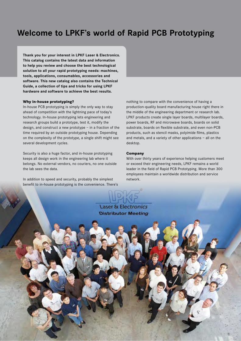
Welcome to LPKF’s world of Rapid PCB Prototyping
nothing to compare with the convenience of having a production-quality board manufacturing house right there in the middle of the engineering department or research lab. LPKF products create single layer boards, multilayer boards, power boards, RF and microwave boards, boards on solid substrate, boards on flexible substrate, and even non-PCB products, such as stencil masks, polyimide films, plastics and metals, and a variety of other applications – all on the desktop.
Company With over thirty years of experience helping customers meet or exceed their engineering needs, LPKF remains a world leader in the field of Rapid PCB Prototyping. More than 300 employees maintain a worldwide distribution and service network.
Thank you for your interest in LPKF Laser & Electronics. This catalog contains the latest data and information to help you review and choose the best technological solution to all your rapid prototyping needs: machines, tools, applications, consumables, accessories and software. This new catalog also contains the Technical Guide, a collection of tips and tricks for using LPKF hardware and software to achieve the best results.
� www.lpkf.com See page 124 to locate an LPKF distributor near you.
Plot
ters
Lase
rPl
atin
gSM
T/Fi
nish
ing
Tech
Gui
deIn
dex
Mul
tila
yer
Contents
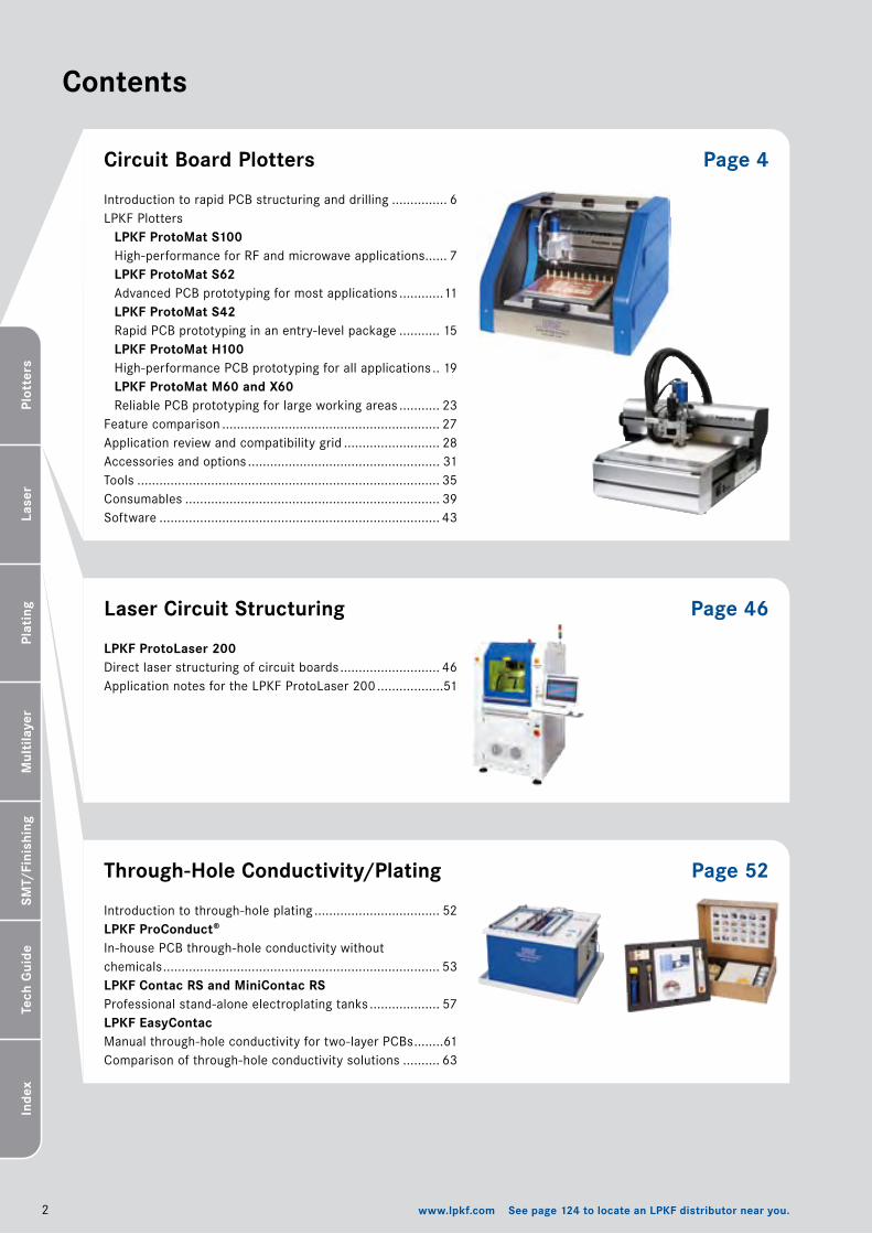
Circuit Board Plotters
Introduction to rapid PCB structuring and drilling ............... 6LPKF Plotters LPKF ProtoMat S100 High-performance for RF and microwave applications ...... 7 LPKF ProtoMat S62 Advanced PCB prototyping for most applications ............�� LPKF ProtoMat S42 Rapid PCB prototyping in an entry-level package ........... �5 LPKF ProtoMat H100 High-performance PCB prototyping for all applications .. �9 LPKF ProtoMat M60 and X60 Reliable PCB prototyping for large working areas ........... �3Feature comparison ........................................................... �7Application review and compatibility grid .......................... �8Accessories and options .................................................... 3�Tools .................................................................................. 35Consumables ..................................................................... 39Software ............................................................................ 43
Laser Circuit Structuring
LPKF ProtoLaser 200Direct laser structuring of circuit boards ........................... 46Application notes for the LPKF ProtoLaser �00 ..................5�
Through-Hole Conductivity/Plating
Page 4
Page 46
Page 52
Introduction to through-hole plating .................................. 5�LPKF ProConduct®In-house PCB through-hole conductivity without chemicals ........................................................................... 53LPKF Contac RS and MiniContac RSProfessional stand-alone electroplating tanks ................... 57LPKF EasyContacManual through-hole conductivity for two-layer PCBs ........6�Comparison of through-hole conductivity solutions .......... 63
Plot
ters
Lase
rPl
atin
gSM
T/Fi
nish
ing
Tech
Gui
de
3
Inde
xM
ulti
laye
r
www.lpkf.com See page 124 to locate an LPKF distributor near you.
Contents
Multilayer Prototyping
Surface Mount Technology/Finishing
Technical Guide
Page 64
Page 68
Page 92
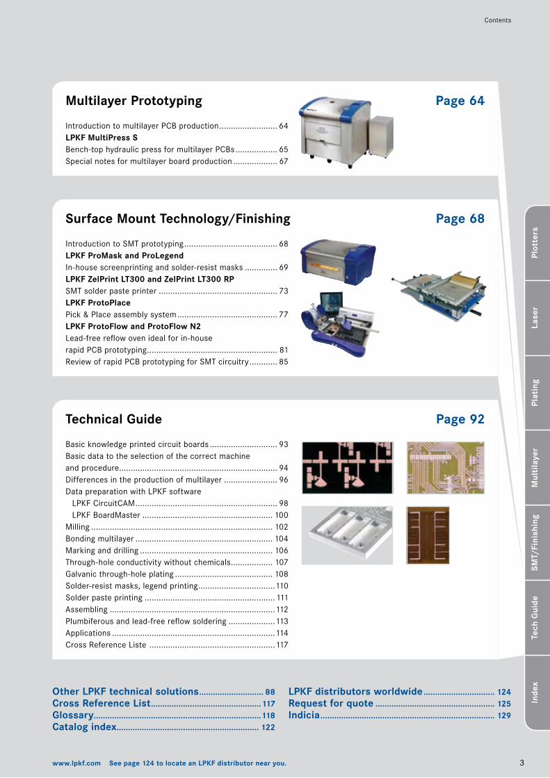
Introduction to multilayer PCB production ......................... 64LPKF MultiPress SBench-top hydraulic press for multilayer PCBs .................. 65Special notes for multilayer board production ................... 67
Introduction to SMT prototyping ........................................ 68LPKF ProMask and ProLegendIn-house screenprinting and solder-resist masks .............. 69LPKF ZelPrint LT300 and ZelPrint LT300 RPSMT solder paste printer ................................................... 73LPKF ProtoPlacePick & Place assembly system ........................................... 77LPKF ProtoFlow and ProtoFlow N2Lead-free reflow oven ideal for in-house rapid PCB prototyping ........................................................ 8�Review of rapid PCB prototyping for SMT circuitry ............ 85
Basic knowledge printed circuit boards ............................. 93Basic data to the selection of the correct machine and procedure .................................................................... 94Differences in the production of multilayer ....................... 96Data preparation with LPKF software LPKF CircuitCAM ............................................................. 98 LPKF BoardMaster ........................................................ �00Milling .............................................................................. �0�Bonding multilayer ........................................................... �04Marking and drilling ......................................................... �06Through-hole conductivity without chemicals .................. �07Galvanic through-hole plating .......................................... �08Solder-resist masks, legend printing .................................��0Solder paste printing ........................................................���Assembling .......................................................................���Plumbiferous and lead-free reflow soldering ....................��3Applications ......................................................................��4Cross Reference Liste ......................................................��7
Other LPKF technical solutions ............................ 88Cross Reference List ................................................117Glossary.........................................................................118Catalog index.............................................................. 122
LPKF distributors worldwide ............................... 124Request for quote .................................................... 125Indicia ............................................................................ 129
4 www.lpkf.com See page 124 to locate an LPKF distributor near you.
Plot
ters
Lase
rPl
atin
gSM
T/Fi
nish
ing
Tech
Gui
deIn
dex
Mul
tila
yer
BoardMasterCircuitCAM
LPKF circuit board plottersfor in-house manufacturing of prototype and small-batch printed circuit boards
LPKF circuit board plotters
Each LPKF circuit board plotter includes a comprehensive software package for importing data from any PCB CAD package and for controlling the plotter.
5www.lpkf.com See page 124 to locate an LPKF distributor near you.
Plot
ters
Lase
rPl
atin
gSM
T/Fi
nish
ing
Tech
Gui
deIn
dex
Mul
tila
yer
Introduction to rapid PCB structuring and drilling . . . . . . . . . . . . . . . . . . . . . . . . . . . . . . . . .6LPKF ProtoMat S100 . . . . . . . . . . . . . . . . . . . . .7 High-performance for RF and microwave applicationsLPKF ProtoMat S62 . . . . . . . . . . . . . . . . . . . . .11 Advanced PCB prototyping for most applicationsLPKF ProtoMat S42 . . . . . . . . . . . . . . . . . . . . 15 Rapid PCB prototyping in an entry-level packageLPKF ProtoMat H100 . . . . . . . . . . . . . . . . . . . .19 High-performance PCB prototyping for all applicationsLPKF ProtoMat M60 and X60 . . . . . . . . . . . . 23 Reliable PCB prototyping for large working areasFeature comparison . . . . . . . . . . . . . . . . . . . . 27Application review and compatibility grid . 28Accessories and options . . . . . . . . . . . . . . . . .31Tools. . . . . . . . . . . . . . . . . . . . . . . . . . . . . . . . . 35Consumables . . . . . . . . . . . . . . . . . . . . . . . . . 39Software . . . . . . . . . . . . . . . . . . . . . . . . . . . . . 43
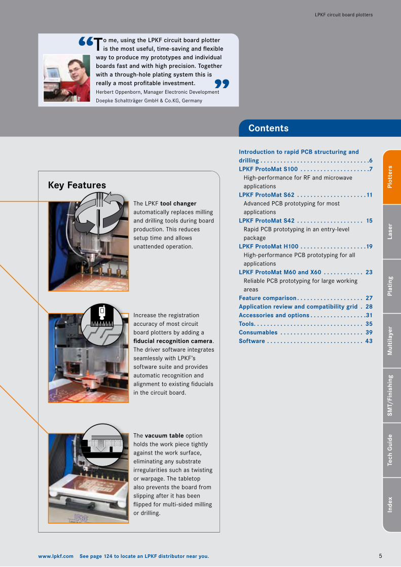
Increase the registration accuracy of most circuit board plotters by adding a fiducial recognition camera. The driver software integrates seamlessly with LPKF’s software suite and provides automatic recognition and alignment to existing fiducials in the circuit board.
The LPKF tool changer automatically replaces milling and drilling tools during board production. This reduces setup time and allows unattended operation.
The vacuum table option holds the work piece tightly against the work surface, eliminating any substrate irregularities such as twisting or warpage. The tabletop also prevents the board from slipping after it has been flipped for multi-sided milling or drilling.
Key Features
Contents
LPKF circuit board plotters
To me, using the LPKF circuit board plotter is the most useful, time-saving and flexible
way to produce my prototypes and individual boards fast and with high precision. Together with a through-hole plating system this is really a most profitable investment. Herbert Oppenborn, Manager Electronic Development
Doepke Schaltträger GmbH & Co.KG, Germany
“”
6 www.lpkf.com See page 124 to locate an LPKF distributor near you.
Plot
ters
Lase
rPl
atin
gSM
T/Fi
nish
ing
Tech
Gui
deIn
dex
Mul
tila
yer
Introduction to rapid PCB structuring and drilling
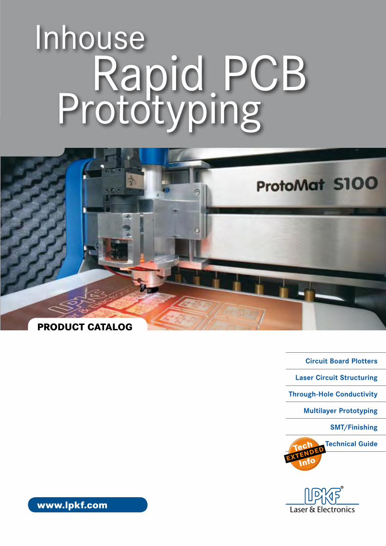
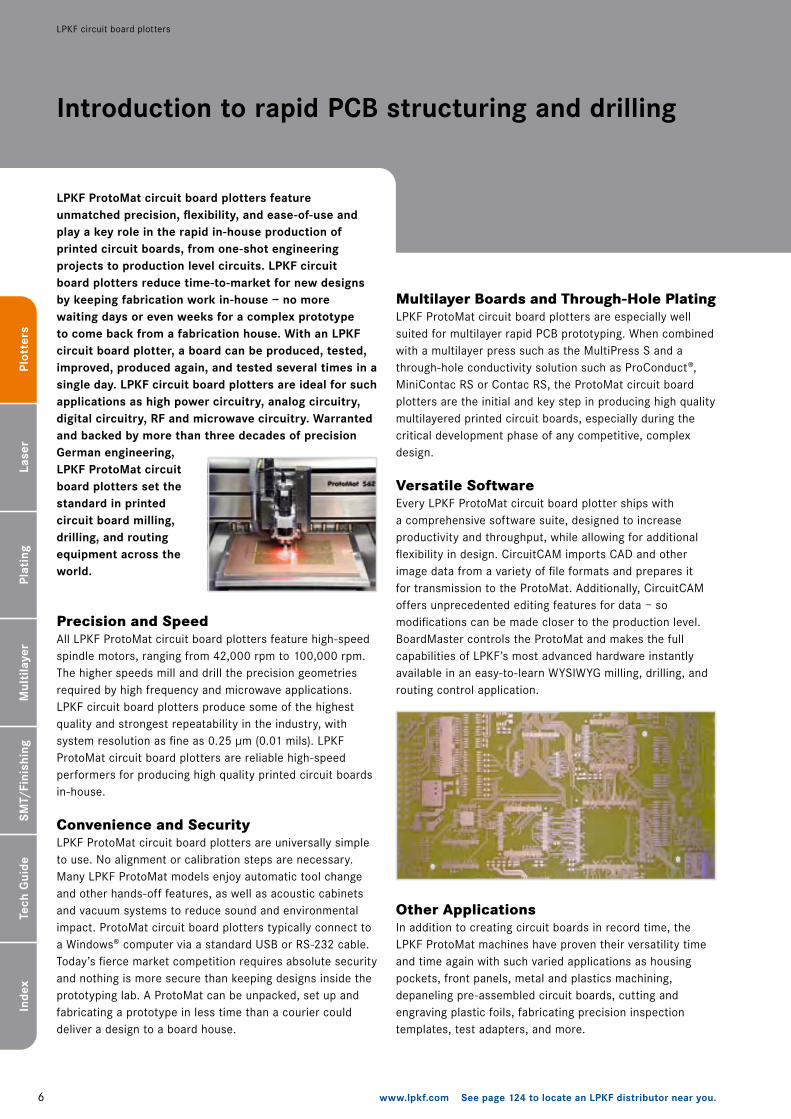
LPKF ProtoMat circuit board plotters feature unmatched precision, flexibility, and ease-of-use and play a key role in the rapid in-house production of printed circuit boards, from one-shot engineering projects to production level circuits. LPKF circuit board plotters reduce time-to-market for new designs by keeping fabrication work in-house – no more waiting days or even weeks for a complex prototype to come back from a fabrication house. With an LPKF circuit board plotter, a board can be produced, tested, improved, produced again, and tested several times in a single day. LPKF circuit board plotters are ideal for such applications as high power circuitry, analog circuitry, digital circuitry, RF and microwave circuitry. Warranted and backed by more than three decades of precision German engineering, LPKF ProtoMat circuit board plotters set the standard in printed circuit board milling, drilling, and routing equipment across the world.
Precision and SpeedAll LPKF ProtoMat circuit board plotters feature high-speed spindle motors, ranging from 4�,000 rpm to �00,000 rpm. The higher speeds mill and drill the precision geometries required by high frequency and microwave applications. LPKF circuit board plotters produce some of the highest quality and strongest repeatability in the industry, with system resolution as fine as 0.�5 µm (0.0� mils). LPKF ProtoMat circuit board plotters are reliable high-speed performers for producing high quality printed circuit boards in-house.
Convenience and SecurityLPKF ProtoMat circuit board plotters are universally simple to use. No alignment or calibration steps are necessary. Many LPKF ProtoMat models enjoy automatic tool change and other hands-off features, as well as acoustic cabinets and vacuum systems to reduce sound and environmental impact. ProtoMat circuit board plotters typically connect to a Windows® computer via a standard USB or RS-�3� cable. Today’s fierce market competition requires absolute security and nothing is more secure than keeping designs inside the prototyping lab. A ProtoMat can be unpacked, set up and fabricating a prototype in less time than a courier could deliver a design to a board house.
Multilayer Boards and Through-Hole PlatingLPKF ProtoMat circuit board plotters are especially well suited for multilayer rapid PCB prototyping. When combined with a multilayer press such as the MultiPress S and a through-hole conductivity solution such as ProConduct®, MiniContac RS or Contac RS, the ProtoMat circuit board plotters are the initial and key step in producing high quality multilayered printed circuit boards, especially during the critical development phase of any competitive, complex design.
Versatile SoftwareEvery LPKF ProtoMat circuit board plotter ships with a comprehensive software suite, designed to increase productivity and throughput, while allowing for additional flexibility in design. CircuitCAM imports CAD and other image data from a variety of file formats and prepares it for transmission to the ProtoMat. Additionally, CircuitCAM offers unprecedented editing features for data – so modifications can be made closer to the production level. BoardMaster controls the ProtoMat and makes the full capabilities of LPKF’s most advanced hardware instantly available in an easy-to-learn WYSIWYG milling, drilling, and routing control application.
Other ApplicationsIn addition to creating circuit boards in record time, the LPKF ProtoMat machines have proven their versatility time and time again with such varied applications as housing pockets, front panels, metal and plastics machining, depaneling pre-assembled circuit boards, cutting and engraving plastic foils, fabricating precision inspection templates, test adapters, and more.
LPKF circuit board plotters
S100
AUTOMATICTOOL CHANGEAUTOMATICTOOL CHANGE
7www.lpkf.com See page 124 to locate an LPKF distributor near you.
Plot
ters
Lase
rPl
atin
gSM
T/Fi
nish
ing
Tech
Gui
deIn
dex
Mul
tila
yer
LPKF ProtoMat S�00
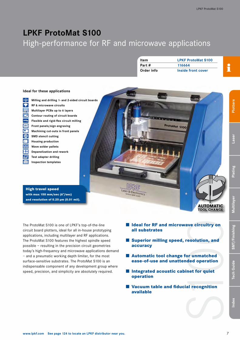
Item LPKF ProtoMat S100Part # 116664Order info Inside front cover
LPKF ProtoMat S100 High-performance for RF and microwave applications
The ProtoMat S�00 is one of LPKF’s top-of-the-line circuit board plotters, ideal for all in-house prototyping applications, including multilayer and RF applications. The ProtoMat S�00 features the highest spindle speed possible – resulting in the precision circuit geometries today’s high-frequency and microwave applications demand – and a pneumatic working depth limiter, for the most surface-sensitive substrates. The ProtoMat S�00 is an indispensable component of any development group where speed, precision, and simplicity are absolutely required.
Ideal for these applications
Milling and drilling 1- and 2-sided circuit boards
RF & microwave circuits
Multilayer PCBs up to 6 layers
Contour routing of circuit boards
Flexible and rigid-flex circuit milling
Front panels/sign engraving
Machining cut-outs in front panels
SMD stencil cutting
Housing production
Wave solder pallets
Depanelization and rework
Test adapter drilling
Inspection templates
Ideal for RF and microwave circuitry on all substrates
Superior milling speed, resolution, and accuracy
Automatic tool change for unmatched ease-of-use and unattended operation
Integrated acoustic cabinet for quiet operation
Vacuum table and fiducial recognition available
High travel speedwith max 150 mm/sec (6”/sec)
and resolution of 0.25 µm (0.01 mil).
100000 rpm
8 www.lpkf.com See page 124 to locate an LPKF distributor near you.
Plot
ters
Lase
rPl
atin
gSM
T/Fi
nish
ing
Tech
Gui
deIn
dex
Mul
tila
yer
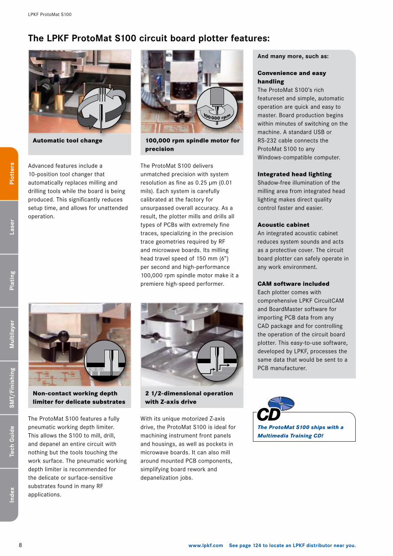
Non-contact working depth limiter for delicate substrates
The ProtoMat S�00 features a fully pneumatic working depth limiter. This allows the S�00 to mill, drill, and depanel an entire circuit with nothing but the tools touching the work surface. The pneumatic working depth limiter is recommended for the delicate or surface-sensitive substrates found in many RF applications.
Convenience and easy handlingThe ProtoMat S�00’s rich featureset and simple, automatic operation are quick and easy to master. Board production begins within minutes of switching on the machine. A standard USB or RS-�3� cable connects the ProtoMat S�00 to any Windows-compatible computer.
2 1/2-dimensional operation with Z-axis drive
With its unique motorized Z-axis drive, the ProtoMat S�00 is ideal for machining instrument front panels and housings, as well as pockets in microwave boards. It can also mill around mounted PCB components, simplifying board rework and depanelization jobs.
Integrated head lightingShadow-free illumination of the milling area from integrated head lighting makes direct quality control faster and easier.
100,000 rpm spindle motor for precision
The ProtoMat S�00 delivers unmatched precision with system resolution as fine as 0.�5 µm (0.0� mils). Each system is carefully calibrated at the factory for unsurpassed overall accuracy. As a result, the plotter mills and drills all types of PCBs with extremely fine traces, specializing in the precision trace geometries required by RF and microwave boards. Its milling head travel speed of �50 mm (6”) per second and high-performance �00,000 rpm spindle motor make it a premiere high-speed performer.
Automatic tool change
Advanced features include a �0-position tool changer that automatically replaces milling and drilling tools while the board is being produced. This significantly reduces setup time, and allows for unattended operation.
Acoustic cabinetAn integrated acoustic cabinet reduces system sounds and acts as a protective cover. The circuit board plotter can safely operate in any work environment.
LPKF ProtoMat S�00
And many more, such as:
CAM software includedEach plotter comes with comprehensive LPKF CircuitCAM and BoardMaster software for importing PCB data from any CAD package and for controlling the operation of the circuit board plotter. This easy-to-use software, developed by LPKF, processes the same data that would be sent to a PCB manufacturer.
The LPKF ProtoMat S100 circuit board plotter features:
The ProtoMat S100 ships with a Multimedia Training CD!
9www.lpkf.com See page 124 to locate an LPKF distributor near you.
Plot
ters
Lase
rPl
atin
gSM
T/Fi
nish
ing
Tech
Gui
deIn
dex
Mul
tila
yer
LPKF ProtoMat S�00
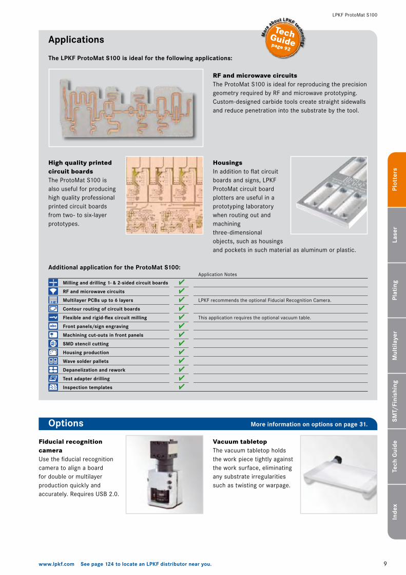
The LPKF ProtoMat S100 is ideal for the following applications:
Applications
RF and microwave circuitsThe ProtoMat S�00 is ideal for reproducing the precision geometry required by RF and microwave prototyping. Custom-designed carbide tools create straight sidewalls and reduce penetration into the substrate by the tool.
High quality printed circuit boardsThe ProtoMat S�00 is also useful for producing high quality professional printed circuit boards from two- to six-layer prototypes.
Fiducial recognition cameraUse the fiducial recognition camera to align a board for double or multilayer production quickly and accurately. Requires USB �.0.
Vacuum tabletopThe vacuum tabletop holds the work piece tightly against the work surface, eliminating any substrate irregularities such as twisting or warpage.
HousingsIn addition to flat circuit boards and signs, LPKF ProtoMat circuit board plotters are useful in a prototyping laboratory when routing out and machining three-dimensional objects, such as housings and pockets in such material as aluminum or plastic.
Additional application for the ProtoMat S100:
Milling and drilling 1- & 2-sided circuit boards
RF and microwave circuits
Multilayer PCBs up to 6 layers
Contour routing of circuit boards
Flexible and rigid-flex circuit milling
Front panels/sign engraving
Machining cut-outs in front panels
SMD stencil cutting
Housing production
Wave solder pallets
Depanelization and rework
Test adapter drilling
Inspection templates
Application Notes
LPKF recommends the optional Fiducial Recognition Camera.
This application requires the optional vacuum table.
Options More information on options on page 31.
�0 www.lpkf.com See page 124 to locate an LPKF distributor near you.
Plot
ters
Lase
rPl
atin
gSM
T/Fi
nish
ing
Tech
Gui
deIn
dex
Mul
tila
yer
LPKF ProtoMat S�00
Part #
Working area (X/Y/Z)
Working area with vacuum table (X/Y/Z)
Resolution (X/Y)
Repeatability
Precision of front-to-back alignment
Milling motor
Tool change
Tool collet
Drilling speed
Travel speed (max)
X/Y positioning system
Z drive
Dimensions (W/H/D)
Weight
Power supply
Compressed air supply
116664
��9 x 305 x 38 mm (9” x ��” x �.5”)
��9 x 305 x �5 mm (9” x ��” x �”)
0.�5 µm (0.0� mil)
±0.00� mm (±0.04 mil)
±0.0� mm (±0.8 mil)
Max. �00,000 rpm, software controlled
Automatic, �0 positions
3.�75 mm (�/8”), pneumatic release collet
�50 strokes/min
Max. �50 mm/sec (6”/sec)
3-phase stepper motors
Stepper motor
670 x 540 x 760 mm (�6.4” x ��.3” x �9.9”)
55 kg (��� lbs)
��5/�30 V, 50–60 Hz, �00 W
6 bar (87 psi), �00 l/min (3.5�8 cfm)
LPKF ProtoMat S100
Specification table
Starter SetContains high-quality tools and consumable material.Multilayer Start-SetEverything needed to start making multilayer boards.Base materialsA collection of copper clad FR4 substrates.
40
41
42
More details on pageConical milling toolsSturdy tooling for all purposes.Cylindrical milling toolsIdeal for RF structuring.Drilling/routing toolsDrilling and depaneling bits.
36
36
37
More details on page
Dust extractionKeeps the work area free of debris of all sizes.CompressorA clean source of compressed air.Measuring microscope 60x magnification for proper alignment.StatusLight Indicates the status of the machine.Brush headRemoves debris from the work area when working in � �/�-dimensional mode.
33
34
33
34
33
More details on page
Accessories Software (included)
Tools Consumables
Accessories, software, tools and consumables
LPKF CircuitCAM PCBA complete workstation for the ProtoMat S�00.LPKF BoardMasterVersatile control software for all ProtoMat models.
44
45
More details on page
Size of tracks and gaps depends on materials and tools. 100 µm tracks and gaps possible with LPKF MicroCutter on FR4 18/18 µm Cu. More information on materials page 93 and tools page 35.
Specifications subject to change.
S62
AUTOMATICTOOL CHANGEAUTOMATICTOOL CHANGE
��www.lpkf.com See page 124 to locate an LPKF distributor near you.
Plot
ters
Lase
rPl
atin
gSM
T/Fi
nish
ing
Tech
Gui
deIn
dex
Mul
tila
yer
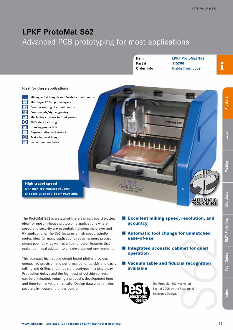
LPKF ProtoMat S62 Advanced PCB prototyping for most applications
LPKF ProtoMat S6�
Item LPKF ProtoMat S62Part # 115788Order info Inside front cover
The ProtoMat S6� is a state-of-the-art circuit board plotter, ideal for most in-house prototyping applications where speed and security are essential, including multilayer and RF applications. The S6� features a high speed spindle motor, ideal for many applications requiring more precise circuit geometry, as well as a host of other features that make it an ideal addition to any development environment.
This compact high-speed circuit board plotter provides unequalled precision and performance for quickly and easily milling and drilling circuit board prototypes in a single day. Production delays and the high cost of outside vendors can be eliminated, reducing a product’s development time and time-to-market dramatically. Design data also remains securely in-house and under control.
Ideal for these applications
Milling and drilling 1- and 2-sided circuit boards
Multilayer PCBs up to 6 layers
Contour routing of circuit boards
Front panels/sign engraving
Machining cut-outs in front panels
SMD stencil cutting
Housing production
Depanelization and rework
Test adapter drilling
Inspection templates
Excellent milling speed, resolution, and accuracy
Automatic tool change for unmatched ease-of-use
Integrated acoustic cabinet for quiet operation
Vacuum table and fiducial recognition available
High travel speedwith max 150 mm/sec (6”/sec)
and resolution of 0.25 µm (0.01 mil).
The ProtoMat S6� was voted
Best of �005 by the Readers of
Electronic Design.
62000 rpm
�� www.lpkf.com See page 124 to locate an LPKF distributor near you.
Plot
ters
Lase
rPl
atin
gSM
T/Fi
nish
ing
Tech
Gui
deIn
dex
Mul
tila
yer
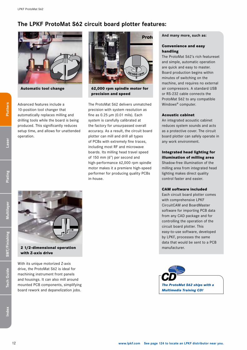
Automatic tool change
Advanced features include a �0-position tool changer that automatically replaces milling and drilling tools while the board is being produced. This significantly reduces setup time, and allows for unattended operation.
Convenience and easy handlingThe ProtoMat S6�’s rich featureset and simple, automatic operation are quick and easy to master. Board production begins within minutes of switching on the machine, and requires no external air compressors. A standard USB or RS-�3� cable connects the ProtoMat S6� to any compatible Windows® computer.
Integrated head lighting for illumination of milling areaShadow-free illumination of the milling area from integrated head lighting makes direct quality control faster and easier.
62,000 rpm spindle motor for precision and speed
The ProtoMat S6� delivers unmatched precision with system resolution as fine as 0.�5 µm (0.0� mils). Each system is carefully calibrated at the factory for unsurpassed overall accuracy. As a result, the circuit board plotter can mill and drill all types of PCBs with extremely fine traces, including most RF and microwave boards. Its milling head travel speed of �50 mm (6”) per second and high-performance 6�,000 rpm spindle motor makes it a premiere high-speed performer for producing quality PCBs in-house.
Acoustic cabinetAn integrated acoustic cabinet reduces system sounds and acts as a protective cover. The circuit board plotter can safely operate in any work environment.
LPKF ProtoMat S6�
CAM software includedEach circuit board plotter comes with comprehensive LPKF CircuitCAM and BoardMaster software for importing PCB data from any CAD package and for controlling the operation of the circuit board plotter. This easy-to-use software, developed by LPKF, processes the same data that would be sent to a PCB manufacturer.2 1/2-dimensional operation
with Z-axis drive
With its unique motorized Z-axis drive, the ProtoMat S6� is ideal for machining instrument front panels and housings. It can also mill around mounted PCB components, simplifying board rework and depanelization jobs.
The LPKF ProtoMat S62 circuit board plotter features:
And many more, such as:
The ProtoMat S62 ships with a Multimedia Training CD!
�3www.lpkf.com See page 124 to locate an LPKF distributor near you.
Plot
ters
Lase
rPl
atin
gSM
T/Fi
nish
ing
Tech
Gui
deIn
dex
Mul
tila
yer
LPKF ProtoMat S6�
Although the LPKF ProtoMat S62 is an excellent tool for a wide variety of applications, it is particularly well-suited for:
Additional applications for the LPKF ProtoMat S62:
Applications
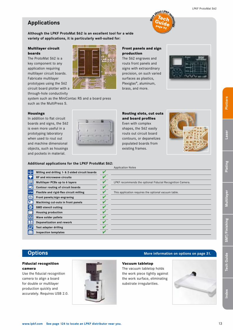
Multilayer circuit boardsThe ProtoMat S6� is a key component to any application requiring multilayer circuit boards. Fabricate multilayer prototypes using the S6� circuit board plotter with a through-hole conductivity system such as the MiniContac RS and a board press such as the MultiPress S.
Front panels and sign productionThe S6� engraves and routs front panels and signs with extraordinary precision, on such varied surfaces as plastics, Plexiglas®, aluminum, brass, and more.
HousingsIn addition to flat circuit boards and signs, the S6� is even more useful in a prototyping laboratory when used to rout out and machine dimensional objects, such as housings and pockets in material.
Routing slots, cut outs and board profilesEven with complex shapes, the S6� easily routs out circuit board contours, or depanelizes populated boards from existing frames.
Fiducial recognition cameraUse the fiducial recognition camera to align a board for double or multilayer production quickly and accurately. Requires USB �.0.
Vacuum tabletopThe vacuum tabletop holds the work piece tightly against the work surface, eliminating substrate irregularities.
Milling and drilling 1- & 2-sided circuit boards
RF and microwave circuits
Multilayer PCBs up to 6 layers
Contour routing of circuit boards
Flexible and rigid-flex circuit milling
Front panels/sign engraving
Machining cut-outs in front panels
SMD stencil cutting
Housing production
Wave solder pallets
Depanelization and rework
Test adapter drilling
Inspection templates
Application Notes
LPKF recommends the optional Fiducial Recognition Camera.
This application requires the optional vacuum table.
Options More information on options on page 31.
�4 www.lpkf.com See page 124 to locate an LPKF distributor near you.
Plot
ters
Lase
rPl
atin
gSM
T/Fi
nish
ing
Tech
Gui
deIn
dex
Mul
tila
yer
LPKF ProtoMat S6�
More details on pageConical milling toolsSturdy tooling for all purposes.Cylindrical milling toolsIdeal for RF structuring and big rubouts.Drilling/routing toolsDrilling and depaneling bits.
36
36
37
More details on page
Dust extractionKeeps the work area free of debris of all sizes.Measuring microscope 60x magnification for proper alignment.StatusLight Indicates the status of the machine.Brush headRemoves debris from the work area when working in � �/�-dimensional mode.
33
33
34
33
More details on page
Accessories Software (included)
Tools Consumables
Accessories, software, tools and consumables
LPKF CircuitCAM PCBA complete workstation for the ProtoMat S6�.LPKF BoardMaster Versatile control software for all ProtoMat models.
44
45
More details on page
Part #
Working area (X/Y/Z)
Working area with vacuum table (X/Y/Z)
Resolution (X/Y)
Repeatability
Precision of front-to-back alignment
Milling motor
Tool change
Tool collet
Drilling speed
Travel speed (max)
X/Y positioning system
Z drive
Dimensions (W/H/D)
Weight
Power supply
Compressed air supply
115788
��9 x 305 x 38 mm (9” x ��” x �.5”)
��9 x 305 x �5 mm (9” x ��” x �”)
0.�5 µm (0.0� mil)
±0.00� mm (±0.04 mil)
±0.0� mm (±0.8 mil)
Max. 6�,000 rpm, software controlled
Automatic, �0 positions
3.�75 mm (�/8”)
�50 strokes/min
Max. �50 mm/sec (6”/sec)
3-phase stepper motors
Stepper motor
670 x 540 x 760 mm (�6.4” x ��.3” x �9.9”)
55 kg (��� lbs)
��5/�30 V, 50–60 Hz, �00 W
Not required
LPKF ProtoMat S62
Specification table
Size of tracks and gaps depends on materials and tools. 100 µm tracks and gaps possible with LPKF MicroCutter on FR4 18/18 µm Cu. More information on materials page 93 and tools page 35.
Specifications subject to change.
Starter SetContains high-quality tools and consumable material.Multilayer Start-SetEverything needed to start making multilayer boards.Base materialsA collection of copper clad FR4 substrates.
40
41
42
S42
�5www.lpkf.com See page 124 to locate an LPKF distributor near you.
Plot
ters
Lase
rPl
atin
gSM
T/Fi
nish
ing
Tech
Gui
deIn
dex
Mul
tila
yer
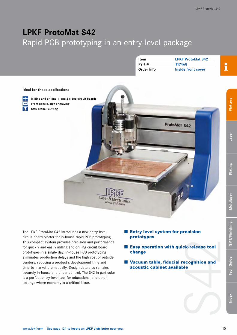
Item LPKF ProtoMat S42Part # 117468Order info Inside front cover
LPKF ProtoMat S4�
LPKF ProtoMat S42 Rapid PCB prototyping in an entry-level package
The LPKF ProtoMat S4� introduces a new entry-level circuit board plotter for in-house rapid PCB prototyping. This compact system provides precision and performance for quickly and easily milling and drilling circuit board prototypes in a single day. In-house PCB prototyping eliminates production delays and the high cost of outside vendors, reducing a product’s development time and time-to-market dramatically. Design data also remains securely in-house and under control. The S4� in particular is a perfect entry-level tool for educational and other settings where economy is a critical issue.
Ideal for these applications
Milling and drilling 1- and 2-sided circuit boards
Front panels/sign engraving
SMD stencil cutting
Entry level system for precision prototypes
Easy operation with quick-release tool change
Vacuum table, fiducial recognition and acoustic cabinet available
42000 rpm
�6 www.lpkf.com See page 124 to locate an LPKF distributor near you.
Plot
ters
Lase
rPl
atin
gSM
T/Fi
nish
ing
Tech
Gui
deIn
dex
Mul
tila
yer
Integrated head lighting for illumination of milling area
Shadow-free illumination of the milling area from integrated head lighting makes direct quality control faster and easier.
Convenience and easy handlingThe ProtoMat S4�’s simple operation is quick and easy to master. Board production begins within minutes of switching on the machine, and it requires no external air compressors or other products. A standard USB or RS-�3� cable connects the ProtoMat S4� to any compatible Windows® computer.
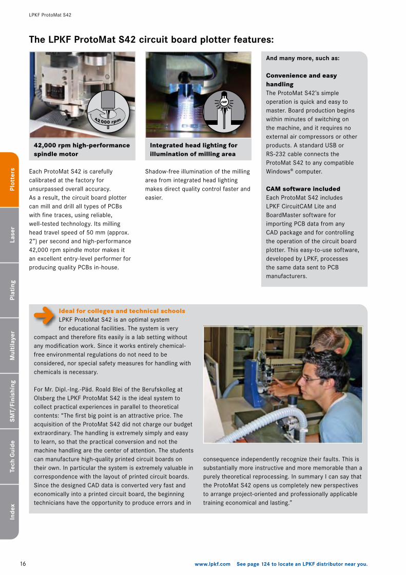
42,000 rpm high-performancespindle motor
Each ProtoMat S4� is carefully calibrated at the factory for unsurpassed overall accuracy. As a result, the circuit board plotter can mill and drill all types of PCBs with fine traces, using reliable, well-tested technology. Its milling head travel speed of 50 mm (approx. �”) per second and high-performance 4�,000 rpm spindle motor makes it an excellent entry-level performer for producing quality PCBs in-house.
The LPKF ProtoMat S42 circuit board plotter features:
LPKF ProtoMat S4�
And many more, such as:
CAM software includedEach ProtoMat S4� includes LPKF CircuitCAM Lite and BoardMaster software for importing PCB data from any CAD package and for controlling the operation of the circuit board plotter. This easy-to-use software, developed by LPKF, processes the same data sent to PCB manufacturers.
Ideal for colleges and technical schoolsLPKF ProtoMat S4� is an optimal system for educational facilities. The system is very
compact and therefore fits easily is a lab setting without any modification work. Since it works entirely chemical-free environmental regulations do not need to be considered, nor special safety measures for handling with chemicals is necessary.
For Mr. Dipl.-Ing.-Päd. Roald Blei of the Berufskolleg at Olsberg the LPKF ProtoMat S4� is the ideal system to collect practical experiences in parallel to theoretical contents: “The first big point is an attractive price. The acquisition of the ProtoMat S4� did not charge our budget extraordinary. The handling is extremely simply and easy to learn, so that the practical conversion and not the machine handling are the center of attention. The students can manufacture high-quality printed circuit boards on their own. In particular the system is extremely valuable in correspondence with the layout of printed circuit boards. Since the designed CAD data is converted very fast and economically into a printed circuit board, the beginning technicians have the opportunity to produce errors and in
consequence independently recognize their faults. This is substantially more instructive and more memorable than a purely theoretical reprocessing. In summary I can say that the ProtoMat S4� opens us completely new perspectives to arrange project-oriented and professionally applicable training economical and lasting.”
�7www.lpkf.com See page 124 to locate an LPKF distributor near you.
Plot
ters
Lase
rPl
atin
gSM
T/Fi
nish
ing
Tech
Gui
deIn
dex
Mul
tila
yer
LPKF ProtoMat S4�
Although the LPKF ProtoMat S42 is an excellent tool for a wide variety of applications, it is particularly well-suited for:
Additional applications for the LPKF ProtoMat S42:
Applications
1- and 2-sided circuit boards on different materialsThe most common use for the LPKF ProtoMat S4� is the production of high-quality professional printed circuit boards on FR4 in a prototyping environment. This system reproduces a prototype accurately from the original design data.
Acoustic cabinetLPKF acoustic cabinets reduce noise and dust emissions, perfect for CAD offices and electronics prototyping labs.
Vacuum tabletopThe vacuum tabletop holds the work piece tightly against the work surface, eliminating substrate irregularities.
Fiducial recognition cameraUse the fiducial recognition camera to align a board for double or multilayer production quickly and accurately. Requires USB �.0.
Milling and drilling 1- & 2-sided circuit boards
RF and microwave circuits
Multilayer PCBs up to 6 layers
Contour routing of circuit boards
Flexible and rigid-flex circuit milling
Front panels/sign engraving
Machining cut-outs in front panels
SMD stencil cutting
Housing production
Wave solder pallets
Depanelization and rework
Test adapter drilling
Inspection templates
Application Notes
LPKF recommends the S6�, S�00, or H�00 for RF/microwave applications.
LPKF recommends the S�00, S6� or H�00 for multilayer boards.
LPKF recommends the use of the S�00, S6�, H�00, M60 or X60.
LPKF recommends the S�00 or S6� with optional vacuum table, or the H�00.
LPKF recommends the S�00 or S6� for routing aluminum front panels.
LPKF recommends the S�00 or S6� with optional vacuum table, or the H�00.
LPKF recommends the S�00 or S6� for high clearances.
LPKF recommends the stepper driven depth controlled S�00 or S6�.
LPKF recommends the S�00 and S6� for rework because of high clearance.
LPKF recommends the stepper driven depth controlled S�00 or S6�.
LPKF recommends an S�00 or H�00 to avoid melting template plastic.
Options More information on options on page 31.
–
–
–
–––––
�8 www.lpkf.com See page 124 to locate an LPKF distributor near you.
Plot
ters
Lase
rPl
atin
gSM
T/Fi
nish
ing
Tech
Gui
deIn
dex
Mul
tila
yer
LPKF ProtoMat S4�
More details on pageConical milling toolsSturdy tooling for all purposes.Cylindrical milling toolsIdeal for big rubouts.Drilling/routing toolsDrilling and depaneling bits.
36
36
37
More details on page
Dust extractionKeeps the work area free of debris of all sizes.Measuring microscope 60x magnification for proper alignment.
33
33
More details on page
Accessories Software (included)
Tools Consumables
Accessories, software, tools and consumables
LPKF CircuitCAM LiteCAM workstation specially for the S4�.LPKF BoardMaster Versatile control software for all ProtoMat models.
44
45
More details on page
Part #
Working area (X/Y/Z)
Resolution (X/Y)
Repeatability
Precision of front-to-back alignment
Milling motor
Tool change
Tool collet
Drilling speed
Travel speed (max.)
X/Y positioning system
Z drive
Dimensions (W/H/D)
Weight
Power supply
Compressed air supply
117468
��9 x 305 x 5 mm (9” x ��” x 0.�”)
� µm (0.04 mil)
±0.005 mm (±0.� mil)
±0.0� mm (±0.8 mil)
Max. 4�,000 rpm, software controlled
Manual, quick-release
3.�75 mm (�/8”)
90 strokes/min
Max. 50 mm/sec (�.97”/sec)
�-phase stepper motors
Electromagnetic, 5 mm (0.�”) stroke
580 x 480 x 6�0 mm (��.8” x �8.9” x �4.4”)
43 kg (95 lbs)
��5/�30 V, 50–60 Hz, �00 W
Not required
LPKF ProtoMat S42
Specification table
Size of tracks and gaps depends on materials and tools. 100 µm tracks and gaps possible with LPKF MicroCutter on FR4 18/18 µm Cu. More information on materials page 93 and tools page 35.
Specifications subject to change.
Starter SetContains high-quality tools and consumable material.Multilayer Start-SetEverything needed to start making multilayer boards.Base materialsA collection of copper clad FR4 substrates.
40
41
42
H100
AUTOMATICTOOL CHANGEAUTOMATICTOOL CHANGE
380 mm (�5”)
365
mm
(�
4.4”
)
�9www.lpkf.com See page 124 to locate an LPKF distributor near you.
Plot
ters
Lase
rPl
atin
gSM
T/Fi
nish
ing
Tech
Gui
deIn
dex
Mul
tila
yer
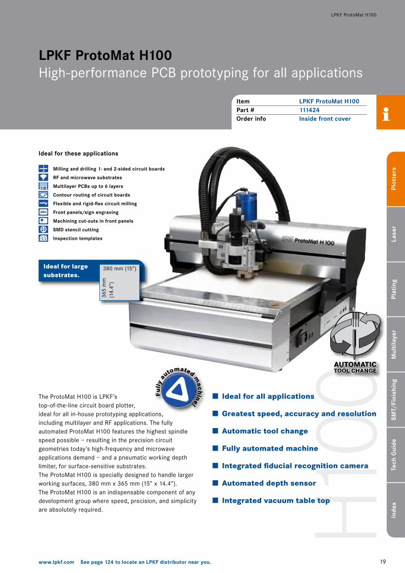
Item LPKF ProtoMat H100Part # 111424Order info Inside front cover
LPKF ProtoMat H�00
LPKF ProtoMat H100 High-performance PCB prototyping for all applications
The ProtoMat H�00 is LPKF’s top-of-the-line circuit board plotter, ideal for all in-house prototyping applications, including multilayer and RF applications. The fully automated ProtoMat H�00 features the highest spindle speed possible – resulting in the precision circuit geometries today’s high-frequency and microwave applications demand – and a pneumatic working depth limiter, for surface-sensitive substrates. The ProtoMat H�00 is specially designed to handle larger working surfaces, 380 mm x 365 mm (�5” x �4.4”). The ProtoMat H�00 is an indispensable component of any development group where speed, precision, and simplicity are absolutely required.
Ideal for these applications
Milling and drilling 1- and 2-sided circuit boards
RF and microwave substrates
Multilayer PCBs up to 6 layers
Contour routing of circuit boards
Flexible and rigid-flex circuit milling
Front panels/sign engraving
Machining cut-outs in front panels
SMD stencil cutting
Inspection templates
Ideal for all applications
Greatest speed, accuracy and resolution
Automatic tool change
Fully automated machine
Integrated fiducial recognition camera
Automated depth sensor
Integrated vacuum table top
Fully
automated m
achine!
Ideal for large substrates.
�0 www.lpkf.com See page 124 to locate an LPKF distributor near you.
Plot
ters
Lase
rPl
atin
gSM
T/Fi
nish
ing
Tech
Gui
deIn
dex
Mul
tila
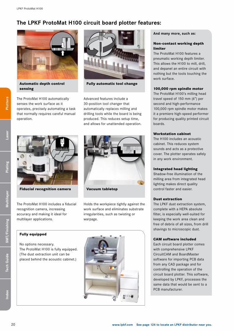
yer Fiducial recognition camera
The ProtoMat H�00 includes a fiducial recognition camera, increasing accuracy and making it ideal for multilayer applications.
Automatic depth control sensing
The ProtoMat H�00 automatically senses the work surface as it operates, precisely automating a task that normally requires careful manual operation.
The LPKF ProtoMat H100 circuit board plotter features:
Vacuum tabletop
Holds the workpiece tightly against the work surface and eliminates substrate irregularities, such as twisting or warpage.
LPKF ProtoMat H�00
Non-contact working depth limiterThe ProtoMat H�00 features a pneumatic working depth limiter. This allows the H�00 to mill, drill, and depanel an entire circuit with nothing but the tools touching the work surface.
Integrated head lightingShadow-free illumination of the milling area from integrated head lighting makes direct quality control faster and easier.
Workstation cabinetThe H�00 includes an acoustic cabinet. This reduces system sounds and acts as a protective cover. The plotter operates safely in any work environment.
Dust extractionThe LPKF dust extraction system, complete with a HEPA absolute filter, is especially well-suited for keeping the work area clean and free of debris of all sizes, from drill shavings to microscopic dust.
And many more, such as:
100,000 rpm spindle motorThe ProtoMat H�00’s milling head travel speed of �50 mm (6”) per second and high-performance �00,000 rpm spindle motor makes it a premiere high-speed performer for producing quality printed circuit boards.
Fully automatic tool change
Advanced features include a 30-position tool changer that automatically replaces milling and drilling tools while the board is being produced. This reduces setup time, and allows for unattended operation.
CAM software includedEach circuit board plotter comes with comprehensive LPKF CircuitCAM and BoardMaster software for importing PCB data from any CAD package and for controlling the operation of the circuit board plotter. This software, developed by LPKF, processes the same data that would be sent to a PCB manufacturer.
Fully equipped
No options necessary. The ProtoMat H�00 is fully equipped. (The dust extraction unit can be placed behind the acoustic cabinet.)
��www.lpkf.com See page 124 to locate an LPKF distributor near you.
Plot
ters
Lase
rPl
atin
gSM
T/Fi
nish
ing
Tech
Gui
deIn
dex
Mul
tila
yer
LPKF ProtoMat H�00
The LPKF ProtoMat H100 is ideal for the following applications:
Additional applications for the ProtoMat H100:
Applications
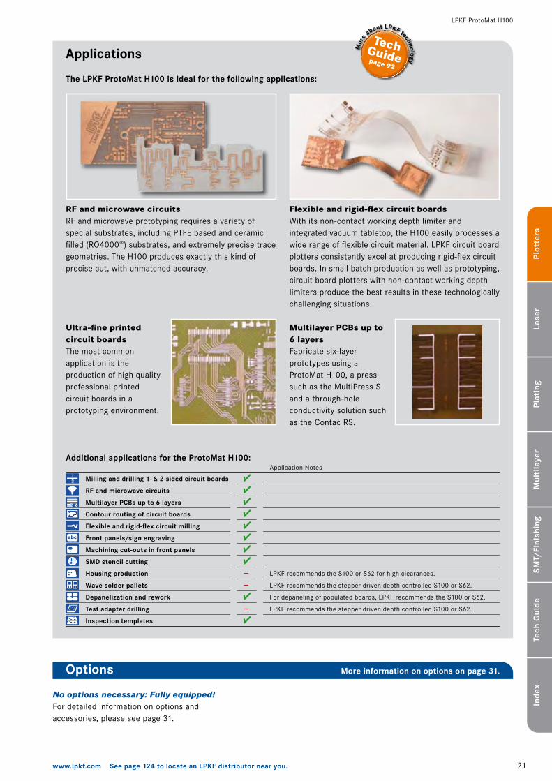
RF and microwave circuitsRF and microwave prototyping requires a variety of special substrates, including PTFE based and ceramic filled (RO4000®) substrates, and extremely precise trace geometries. The H�00 produces exactly this kind of precise cut, with unmatched accuracy.
Flexible and rigid-flex circuit boardsWith its non-contact working depth limiter and integrated vacuum tabletop, the H�00 easily processes a wide range of flexible circuit material. LPKF circuit board plotters consistently excel at producing rigid-flex circuit boards. In small batch production as well as prototyping, circuit board plotters with non-contact working depth limiters produce the best results in these technologically challenging situations.
Ultra-fine printed circuit boardsThe most common application is the production of high quality professional printed circuit boards in a prototyping environment.
No options necessary: Fully equipped!For detailed information on options and accessories, please see page 3�.
Milling and drilling 1- & 2-sided circuit boards
RF and microwave circuits
Multilayer PCBs up to 6 layers
Contour routing of circuit boards
Flexible and rigid-flex circuit milling
Front panels/sign engraving
Machining cut-outs in front panels
SMD stencil cutting
Housing production
Wave solder pallets
Depanelization and rework
Test adapter drilling
Inspection templates
Application Notes
LPKF recommends the S�00 or S6� for high clearances.
LPKF recommends the stepper driven depth controlled S�00 or S6�.
For depaneling of populated boards, LPKF recommends the S�00 or S6�.
LPKF recommends the stepper driven depth controlled S�00 or S6�.
Multilayer PCBs up to 6 layersFabricate six-layer prototypes using a ProtoMat H�00, a press such as the MultiPress S and a through-hole conductivity solution such as the Contac RS.
Options More information on options on page 31.
––
–
�� www.lpkf.com See page 124 to locate an LPKF distributor near you.
Plot
ters
Lase
rPl
atin
gSM
T/Fi
nish
ing
Tech
Gui
deIn
dex
Mul
tila
yer
More details on page
LPKF ProtoMat H�00
Conical milling toolsSturdy tooling for all purposesCylindrical milling toolsIdeal for RF structuring.Drilling/routing toolsDrilling and depaneling bits.
36
36
37
More details on page
CompressorA clean source of compressed air.Measuring microscope 60x magnification for proper alignment.StatusLight Indicates the status of the machine.
34
33
34
More details on page
Accessories Software (included)
Tools Consumables
Accessories, software, tools and consumables
Part #
Working area (X/Y/Z)
Resolution (X/Y)
Repeatability
Precision of front-to-back alignment
Milling motor
Tool change
Tool collet
Drilling speed
Travel speed
X/Y positioning system
Z drive
Dimensions (W/H/D)
Weight
Power supply
Compressed air supply
111424
380 x 365 x �4 mm (�5” x �4.4” x 0.55”)
0.�5 µm (0.0� mil)
±0.00� mm (±0.04 mil)
±0.0� mm (±0.8 mil)
Max. �00,000 rpm, software controlled
Automatic, 30 tools
3.�75 mm (�/8”), pneumatic release collet
��0 strokes/min
Max. �50 mm/sec (6”/sec)
3-phase stepper motors
Pneumatic, �4 mm (0.55”)
650 x 430 x 750 mm (�5.6” x �7” x �9.5”)
50 kg (��0 lbs)
��5/�30 V, 50–60 Hz, �00 W
6 bar (87 psi), �00 l/min (3.5�8 cfm)
LPKF ProtoMat H100
Specification table
LPKF CircuitCAM PCBA complete workstation for the ProtoMat H�00.LPKF BoardMaster Versatile control software for all ProtoMat models.
44
45
More details on page
Size of tracks and gaps depends on materials and tools. 100 µm tracks and gaps possible with LPKF MicroCutter on FR4 18/18 µm Cu. More information on materials page 93 and tools page 35.
Specifications subject to change.
Starter SetContains high-quality tools and consumable material.Multilayer Start-SetEverything needed to start making multilayer boards.Base materialsA collection of copper clad FR4 substrates.
40
41
42
M60
, X60540 mm (��.�5”)
375
mm
(�
4.75
5”)
650 mm (�5.6”)
530
mm
(�0.
8”)
�3www.lpkf.com See page 124 to locate an LPKF distributor near you.
Plot
ters
Lase
rPl
atin
gSM
T/Fi
nish
ing
Tech
Gui
deIn
dex
Mul
tila
yerIdeal for large
substrates.
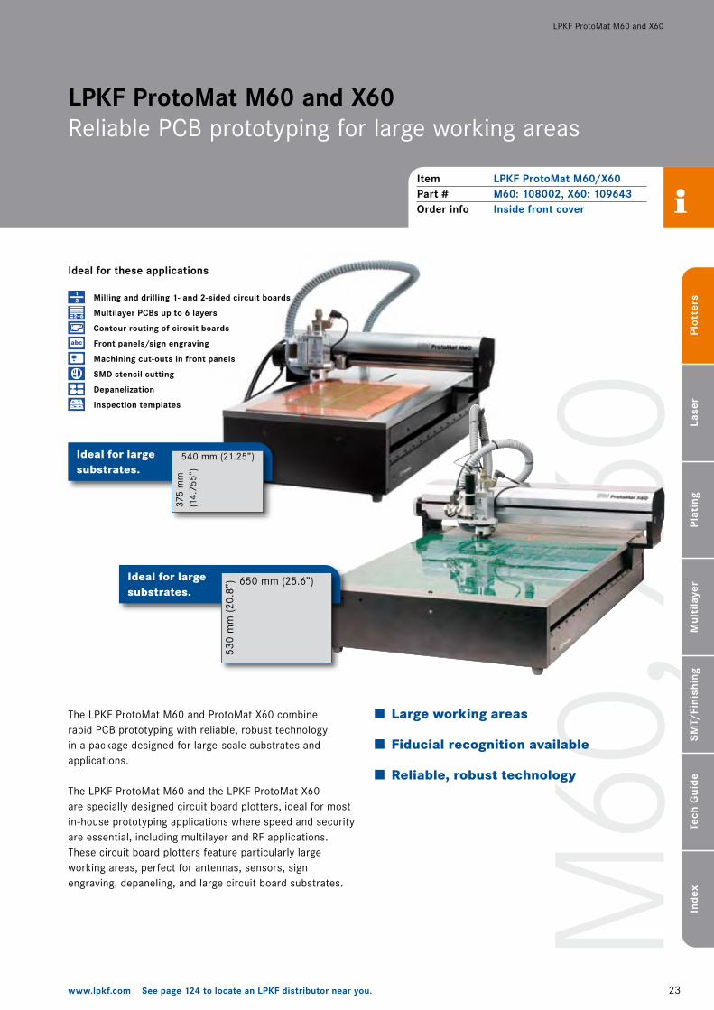
Item LPKF ProtoMat M60/X60Part # M60: 108002, X60: 109643Order info Inside front cover
LPKF ProtoMat M60 and X60
LPKF ProtoMat M60 and X60 Reliable PCB prototyping for large working areas
The LPKF ProtoMat M60 and ProtoMat X60 combine rapid PCB prototyping with reliable, robust technology in a package designed for large-scale substrates and applications.
The LPKF ProtoMat M60 and the LPKF ProtoMat X60 are specially designed circuit board plotters, ideal for most in-house prototyping applications where speed and security are essential, including multilayer and RF applications. These circuit board plotters feature particularly large working areas, perfect for antennas, sensors, sign engraving, depaneling, and large circuit board substrates.
Ideal for these applications
Milling and drilling 1- and 2-sided circuit boards
Multilayer PCBs up to 6 layers
Contour routing of circuit boards
Front panels/sign engraving
Machining cut-outs in front panels
SMD stencil cutting
Depanelization
Inspection templates
Large working areas
Fiducial recognition available
Reliable, robust technology
Ideal for large substrates.
60000 rpm
�4 www.lpkf.com See page 124 to locate an LPKF distributor near you.
Plot
ters
Lase
rPl
atin
gSM
T/Fi
nish
ing
Tech
Gui
deIn
dex
Mul
tila
yer
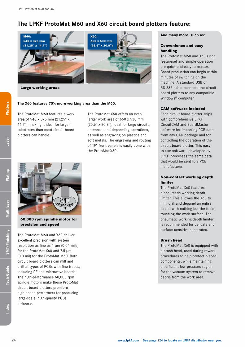
The ProtoMat M60 features a work area of 540 x 375 mm (��.�5” x �4.7”), making it ideal for larger substrates than most circuit board plotters can handle.
Convenience and easy handlingThe ProtoMat M60 and X60’s rich featureset and simple operation are quick and easy to master. Board production can begin within minutes of switching on the machine. A standard USB or RS-�3� cable connects the circuit board plotters to any compatible Windows® computer.
60,000 rpm spindle motor for precision and speed
The ProtoMat M60 and X60 deliver excellent precision with system resolution as fine as � µm (0.04 mils) for the ProtoMat X60 and 7.5 µm (0.3 mil) for the ProtoMat M60. Both circuit board plotters can mill and drill all types of PCBs with fine traces, including RF and microwave boards. The high-performance 60,000 rpm spindle motors make these ProtoMat circuit board plotters premiere high-speed performers for producing large-scale, high-quality PCBs in-house.
The LPKF ProtoMat M60 and X60 circuit board plotters feature:
CAM software includedEach circuit board plotter ships with comprehensive LPKF CircuitCAM and BoardMaster software for importing PCB data from any CAD package and for controlling the operation of the circuit board plotter. This easy-to-use software, developed by LPKF, processes the same data that would be sent to a PCB manufacturer.
LPKF ProtoMat M60 and X60
And many more, such as:M60:540 x 375 mm (21.25” x 14.7”)
Non-contact working depth limiterThe ProtoMat X60 features a pneumatic working depth limiter. This allowes the X60 to mill, drill and depanel an entire circuit with nothing but the tools touching the work surface. The pneumatic working depth limiter is recommended for delicate and surface-sensitive substrates.
Brush headThe ProtoMat X60 is equipped with a brush head, used during rework procedures to help protect placed components, while maintaining a sufficient low-pressure region for the vacuum system to remove debris from the work area.
X60:650 x 530 mm (25.6” x 20.8”)
The ProtoMat X60 offers an even larger work area of 650 x 530 mm (�5.6” x �0.8”), ideal for large circuits, antennas, and depaneling operations, as well as engraving on plastics and soft metals. The engraving and routing of �9” front panels is easily done with the ProtoMat X60.
Large working areas
The X60 features 70% more working area than the M60.
�5www.lpkf.com See page 124 to locate an LPKF distributor near you.
Plot
ters
Lase
rPl
atin
gSM
T/Fi
nish
ing
Tech
Gui
deIn
dex
Mul
tila
yer
Fiducial recognition cameraUse the fiducial recognition camera to align a board for double or multilayer production quickly and accurately. Requires USB �.0.
LPKF ProtoMat M60 and X60
The LPKF ProtoMat M60 and X60 are ideal for the following applications:
Further applications for the LPKF ProtoMat M60 and X60 are:
Applications
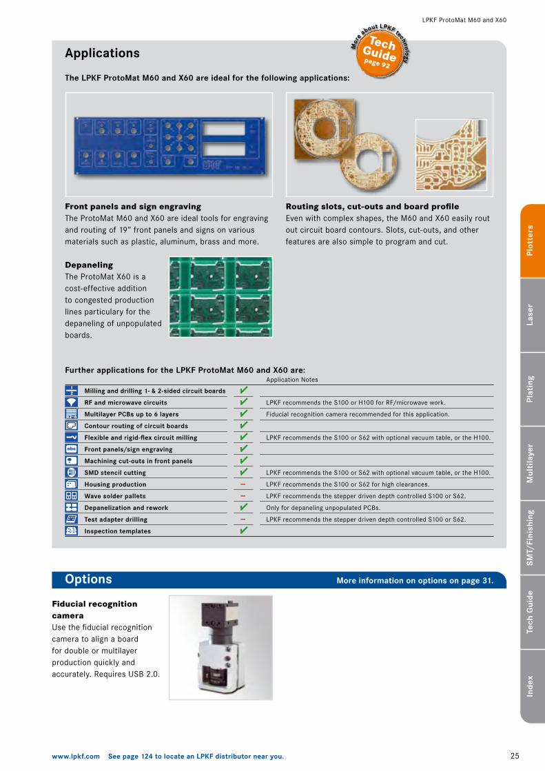
Front panels and sign engravingThe ProtoMat M60 and X60 are ideal tools for engraving and routing of �9” front panels and signs on various materials such as plastic, aluminum, brass and more.
Routing slots, cut-outs and board profileEven with complex shapes, the M60 and X60 easily rout out circuit board contours. Slots, cut-outs, and other features are also simple to program and cut.
Options
DepanelingThe ProtoMat X60 is a cost-effective addition to congested production lines particulary for the depaneling of unpopulated boards.
Milling and drilling 1- & 2-sided circuit boards
RF and microwave circuits
Multilayer PCBs up to 6 layers
Contour routing of circuit boards
Flexible and rigid-flex circuit milling
Front panels/sign engraving
Machining cut-outs in front panels
SMD stencil cutting
Housing production
Wave solder pallets
Depanelization and rework
Test adapter drilling
Inspection templates
Application Notes
LPKF recommends the S�00 or H�00 for RF/microwave work.
Fiducial recognition camera recommended for this application.
LPKF recommends the S�00 or S6� with optional vacuum table, or the H�00.
LPKF recommends the S�00 or S6� with optional vacuum table, or the H�00.
LPKF recommends the S�00 or S6� for high clearances.
LPKF recommends the stepper driven depth controlled S�00 or S6�.
Only for depaneling unpopulated PCBs.
LPKF recommends the stepper driven depth controlled S�00 or S6�.
More information on options on page 31.
––
–
�6 www.lpkf.com See page 124 to locate an LPKF distributor near you.
Plot
ters
Lase
rPl
atin
gSM
T/Fi
nish
ing
Tech
Gui
deIn
dex
Mul
tila
yer
More details on page
LPKF ProtoMat M60 and X60
Conical milling toolsSturdy tooling for all purposesCylindrical milling toolsIdeal for big rubouts.Drilling/routing toolsDrilling and depaneling bits.
36
36
37
More details on page
CompressorA clean source of compressed air.Dust extractionFor keeping the work area clean and free of debris.Measuring microscope 60x magnification for proper alignment.
34
33
33
More details on page
Accessories
Tools Consumables
Accessories, software, tools and consumables
LPKF CircuitCAM PCBA complete workstation for the ProtoMat M60.LPKF BoardMaster Versatile control software for all ProtoMat models.
44
45
More details on page
Part #
Working area (X/Y/Z)
Resolution (X/Y)
Repeatability
Precision of front-to-back alignment
Milling motor
Tool change
Tool collet
Drilling speed
Travel speed (max.)
X/Y positioning system
Z drive
Machine table base
Dimensions (W/H/D)
Weight
Power supply
Compressed air supply
108002
540 x 375 x 5 mm (��” x �5” x 0.�”)
7.937 µm (0.3��5 mil)
±0.005 mm (±0.� mil)
±0.0� mm (±0.8 mil)
Max. 60,000 rpm, software controlled
Manual, quick-release
3.�75 mm (�/8”)
90 strokes/min
40 mm/sec (�.575”/sec)
�-phase stepper motors
Electromagnetic, 5 mm (0.�”)
Precision milled aluminum bed
600 x 375 x 760 mm (�3.6” x �4.75” x 30”)
43 kg (95 lbs)
��5/�30 V, 50–60 Hz, �00 W
None required
LPKF ProtoMat M60
Specification table
Software (included)
Size of tracks and gaps depends on materials and tools. 100 µm tracks and gaps possible with LPKF MicroCutter on FR4 18/18 µm Cu. More information on materials page 93 and tools page 35.
Specifications subject to change.
109643
650 x 530 x �4 mm (�5.6” x �0.8” x 0.55”)
� µm (0.04 mil)
±0.00� mm (±0.04 mil)
±0.0� mm (±0.8 mil)
Max. 60,000 rpm, software controlled
Manual, quick-release
3.�75 mm (�/8”)
��0 strokes/min
�00 mm/sec (3.94”/sec)
3-phase stepper motors
Pneumatic, �4 mm (0.55”)
Precision milled aluminum bed
750 x 4�0 x 900 mm (�9.5” x �6.5” x 35.4”)
69 kg (�5� lbs)
��5/�30 V, 50–60 Hz, �00 W
6 bar (87 psi), �00 l/min (3.5�8 cfm)
LPKF ProtoMat X60
Starter SetContains high-quality tools and consumable material.Multilayer Start-SetEverything needed to start making multilayer boards.Base materialsA collection of copper clad FR4 substrates.
40
41
42
�7www.lpkf.com See page 124 to locate an LPKF distributor near you.
Plot
ters
Lase
rPl
atin
gSM
T/Fi
nish
ing
Tech
Gui
deIn
dex
Mul
tila
yer
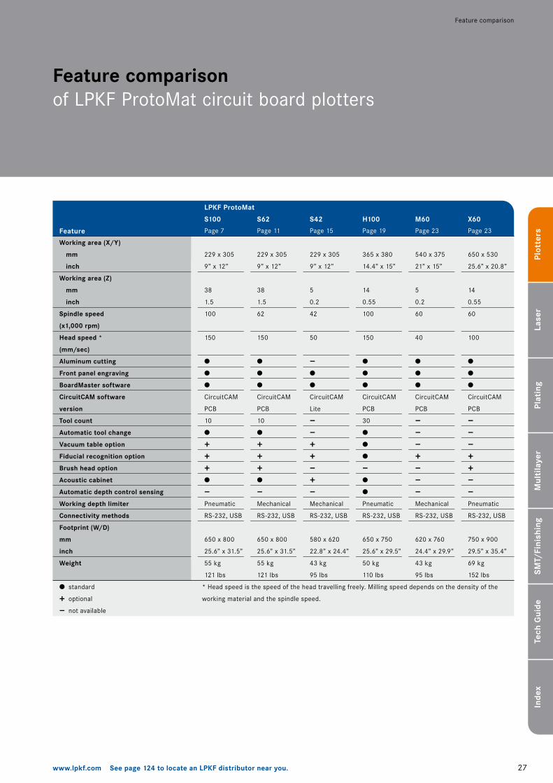
Feature comparison
Working area (X/Y)
mm
inch
Working area (Z)
mm
inch
Spindle speed
(x1,000 rpm)
Head speed *
(mm/sec)
Aluminum cutting
Front panel engraving
BoardMaster software
CircuitCAM software
version
Tool count
Automatic tool change
Vacuum table option
Fiducial recognition option
Brush head option
Acoustic cabinet
Automatic depth control sensing
Working depth limiter
Connectivity methods
Footprint (W/D)
mm
inch
Weight
��9 x 305
9” x ��”
38
�.5
�00
�50
CircuitCAM
PCB
�0
+++
–Pneumatic
RS-�3�, USB
650 x 800
�5.6” x 3�.5”
55 kg
��� lbs
S100
��9 x 305
9” x ��”
38
�.5
6�
�50
CircuitCAM
PCB
�0
+++
–Mechanical
RS-�3�, USB
650 x 800
�5.6” x 3�.5”
55 kg
��� lbs
��9 x 305
9” x ��”
5
0.�
4�
50
–
CircuitCAM
Lite
––++
–+–Mechanical
RS-�3�, USB
580 x 6�0
��.8” x �4.4”
43 kg
95 lbs
S62 S42
LPKF ProtoMat
365 x 380
�4.4” x �5”
�4
0.55
�00
�50
CircuitCAM
PCB
30
–
Pneumatic
RS-�3�, USB
650 x 750
�5.6” x �9.5”
50 kg
��0 lbs
H100
540 x 375
��” x �5”
5
0.�
60
40
CircuitCAM
PCB
–––+–––Mechanical
RS-�3�, USB
6�0 x 760
�4.4” x �9.9”
43 kg
95 lbs
M60
650 x 530
�5.6” x �0.8”
�4
0.55
60
�00
CircuitCAM
PCB
–––++––Pneumatic
RS-�3�, USB
750 x 900
�9.5” x 35.4”
69 kg
�5� lbs
X60
Feature Page 7 Page �� Page �5 Page �9 Page �3 Page �3
Feature comparison of LPKF ProtoMat circuit board plotters
* Head speed is the speed of the head travelling freely. Milling speed depends on the density of the
working material and the spindle speed.
standard
+ optional
– not available
�8 www.lpkf.com See page 124 to locate an LPKF distributor near you.
Plot
ters
Lase
rPl
atin
gSM
T/Fi
nish
ing
Tech
Gui
deIn
dex
Mul
tila
yer
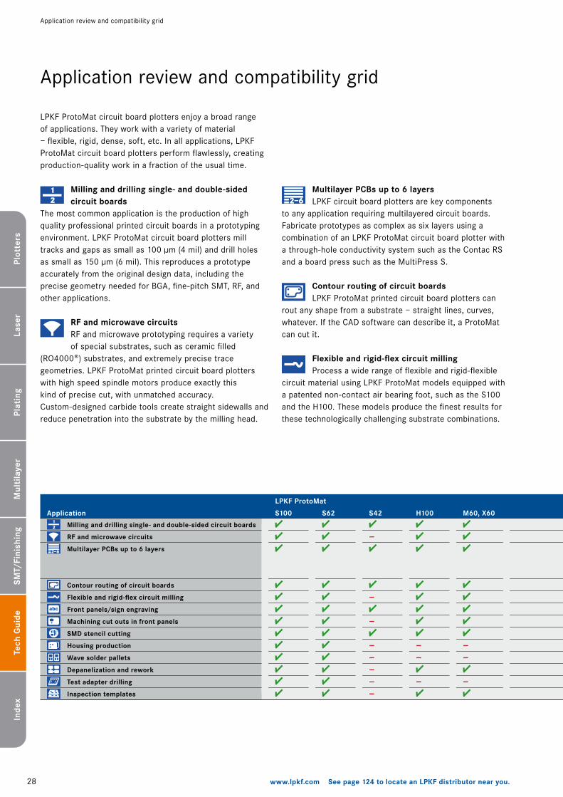
Application review and compatibility grid
Application review and compatibility grid
LPKF ProtoMat circuit board plotters enjoy a broad range of applications. They work with a variety of material – flexible, rigid, dense, soft, etc. In all applications, LPKF ProtoMat circuit board plotters perform flawlessly, creating production-quality work in a fraction of the usual time.
Milling and drilling single- and double-sided circuit boards
The most common application is the production of high quality professional printed circuit boards in a prototyping environment. LPKF ProtoMat circuit board plotters mill tracks and gaps as small as �00 µm (4 mil) and drill holes as small as �50 µm (6 mil). This reproduces a prototype accurately from the original design data, including the precise geometry needed for BGA, fine-pitch SMT, RF, and other applications.
RF and microwave circuitsRF and microwave prototyping requires a variety of special substrates, such as ceramic filled
(RO4000®) substrates, and extremely precise trace geometries. LPKF ProtoMat printed circuit board plotters with high speed spindle motors produce exactly this kind of precise cut, with unmatched accuracy. Custom-designed carbide tools create straight sidewalls and reduce penetration into the substrate by the milling head.
Multilayer PCBs up to 6 layersLPKF circuit board plotters are key components
to any application requiring multilayered circuit boards. Fabricate prototypes as complex as six layers using a combination of an LPKF ProtoMat circuit board plotter with a through-hole conductivity system such as the Contac RS and a board press such as the MultiPress S.
Contour routing of circuit boardsLPKF ProtoMat printed circuit board plotters can
rout any shape from a substrate – straight lines, curves, whatever. If the CAD software can describe it, a ProtoMat can cut it.
Flexible and rigid-flex circuit millingProcess a wide range of flexible and rigid-flexible
circuit material using LPKF ProtoMat models equipped with a patented non-contact air bearing foot, such as the S�00 and the H�00. These models produce the finest results for these technologically challenging substrate combinations.
Application
Milling and drilling single- and double-sided circuit boards
RF and microwave circuits
Multilayer PCBs up to 6 layers
Contour routing of circuit boards
Flexible and rigid-flex circuit milling
Front panels/sign engraving
Machining cut outs in front panels
SMD stencil cutting
Housing production
Wave solder pallets
Depanelization and rework
Test adapter drilling
Inspection templates
S100 S62 S42
LPKF ProtoMat
H100 M60, X60
–
–
–
–––––
––
–
––
–
�9www.lpkf.com See page 124 to locate an LPKF distributor near you.
Plot
ters
Lase
rPl
atin
gSM
T/Fi
nish
ing
Tech
Gui
deIn
dex
Mul
tila
yer
Application review and compatibility grid
LPKF recommends the S�00 or H�00 when the primary application is RF/microwave.
LPKF recommends the increased accuracy and ease-of-use afforded by the optional fiducial recognition camera (the camera is standard with
the H�00).
Note that the LPKF MultiPress S, required for pressing 4+ layer boards, has a maximum layout area of �00 x �75 mm (7.8” x �0.8”).
Working with flexible substrates requires a vacuum table, an option on the S6� and the S�00. A vacuum table is a standard feature of the H�00.
LPKF recommends the S�00 or S6� for routing aluminum front panels.
Working with flexible substrates requires a vacuum table, an option on the S6� and the S�00. A vacuum table is a standard feature of the H�00.
LPKF recommends the S�00 and S6� for the high clearances necessary for plastic and aluminum housings.
LPKF recommends the S�00 or S6� with stepper controlled z-axis and a high clearance.
LPKF recommends the S�00 and S6� for rework because of the high clearance, however the M60 and X60 will depanel unpopulated PCBs.
LPKF recommends the S�00 or S6� for the stepper controlled Z-axis and high clearance.
LPKF recommends an S�00 or other high-speed ProtoMat to avoid melting template plastic.
Application Notes
Front panels/sign engravingLPKF ProtoMat circuit board plotters engrave front
panels and signs with extraordinary precision, on plastics, Plexiglas, aluminum, brass, and more.
Machining cut outs in front panelsLPKF ProtoMat circuit board plotters with fast
spindle speed motors rout aluminum front panels quickly and easily.
SMD stencil cuttingIn the mass production of SMT circuit boards,
the use of polyimide solder masks is critical, driving the precision of solder application and protecting the board from environmental influences.
Housing productionIn addition to flat circuit boards and signs, LPKF
ProtoMat circuit board plotters are useful in a prototyping lab when routing out and machining three-dimensional objects, such as housings and pockets in material.
Wave solder palletsWave solder pallets hold PCBs steady during wave
soldering. LPKF ProtoMat circuit board plotters with stepper motor Z-axis control are ideal for routing and milling support structures in thick, temperature-resistant plastics.
Depanelization and reworkAn LPKF ProtoMat can be a valuable element in a
fast-paced production environment, providing independent depaneling of populated and unpopulated circuit boards. ProtoMat circuit board plotters are also excellent for certain kinds of rework and circuit tuning.
Test adapter drillingBed-of-nails testing platforms require custom fabricated plastic adaptors, and high speed LPKF
ProtoMat circuit board plotters with stepper motors controlling the Z-axis are perfect for this application.
Inspection templatesLPKF ProtoMat circuit board plotters are well suited
for the precise machining of solder frames and inspection templates – two crucial elements of quality control in the mass production of printed circuit boards.
30 www.lpkf.com See page 124 to locate an LPKF distributor near you.
Plot
ters
Lase
rPl
atin
gSM
T/Fi
nish
ing
Tech
Gui
deIn
dex
Mul
tila
yer
Introduction to ProtoMat accessories, options, tools, and consumables
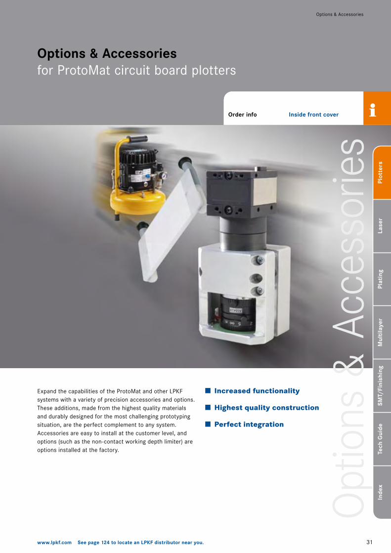
Options & AccessoriesExpand the functionality of an LPKF ProtoMat circuit board plotter (and other LPKF equipment) with a variety of precision accessories. Install accessories (such as acoustic cabinets, etc.) onsite and in a matter of minutes.
Most every LPKF ProtoMat circuit board plotter can be enhanced before it ever leaves the factory with the addition of a number of factory-installed options (such as non-contact air-bearing depth limiter). All options are custom-designed to perfectly complement and enhance an LPKF system.
Introduction to ProtoMat accessories, options, tools, and consumables
Options & Accessories. . . . . . . . . . . . . . . . . . .31 for the ProtoMat circuit board plottersTools. . . . . . . . . . . . . . . . . . . . . . . . . . . . . . . . . 35 Reliable tooling for the ProtoMat circuit board plottersConsumables . . . . . . . . . . . . . . . . . . . . . . . . . 39 for the ProtoMat circuit board plotters
Contents
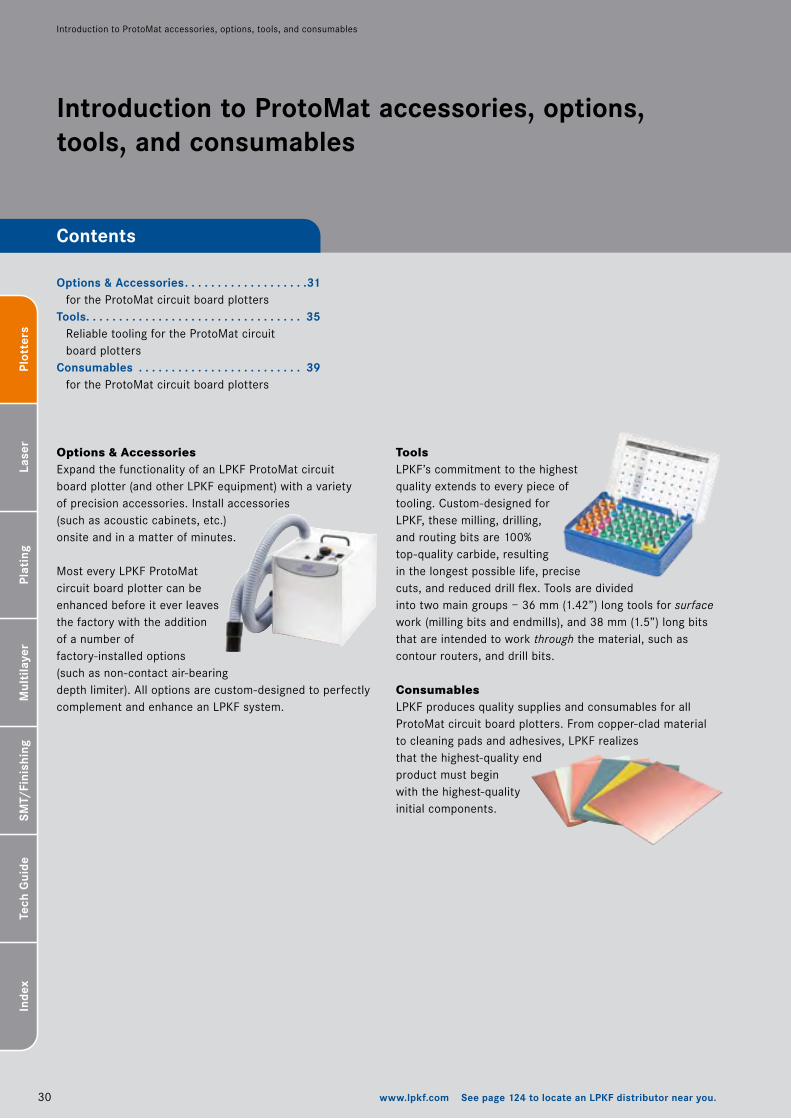
ToolsLPKF’s commitment to the highest quality extends to every piece of tooling. Custom-designed for LPKF, these milling, drilling, and routing bits are �00% top-quality carbide, resulting in the longest possible life, precise cuts, and reduced drill flex. Tools are divided into two main groups – 36 mm (�.4�”) long tools for surface work (milling bits and endmills), and 38 mm (�.5”) long bits that are intended to work through the material, such as contour routers, and drill bits.
ConsumablesLPKF produces quality supplies and consumables for all ProtoMat circuit board plotters. From copper-clad material to cleaning pads and adhesives, LPKF realizes that the highest-quality end product must begin with the highest-quality initial components.
Opt
ions
& A
cces
sorie
s
3�www.lpkf.com See page 124 to locate an LPKF distributor near you.
Plot
ters
Lase
rPl
atin
gSM
T/Fi
nish
ing
Tech
Gui
deIn
dex
Mul
tila
yer
Order info Inside front cover
Options & Accessories
Options & Accessories for ProtoMat circuit board plotters
Expand the capabilities of the ProtoMat and other LPKF systems with a variety of precision accessories and options. These additions, made from the highest quality materials and durably designed for the most challenging prototyping situation, are the perfect complement to any system. Accessories are easy to install at the customer level, and options (such as the non-contact working depth limiter) are options installed at the factory.
Increased functionality
Highest quality construction
Perfect integration
3� www.lpkf.com See page 124 to locate an LPKF distributor near you.
Plot
ters
Lase
rPl
atin
gSM
T/Fi
nish
ing
Tech
Gui
deIn
dex
Mul
tila
yer
Options & Accessories
Options
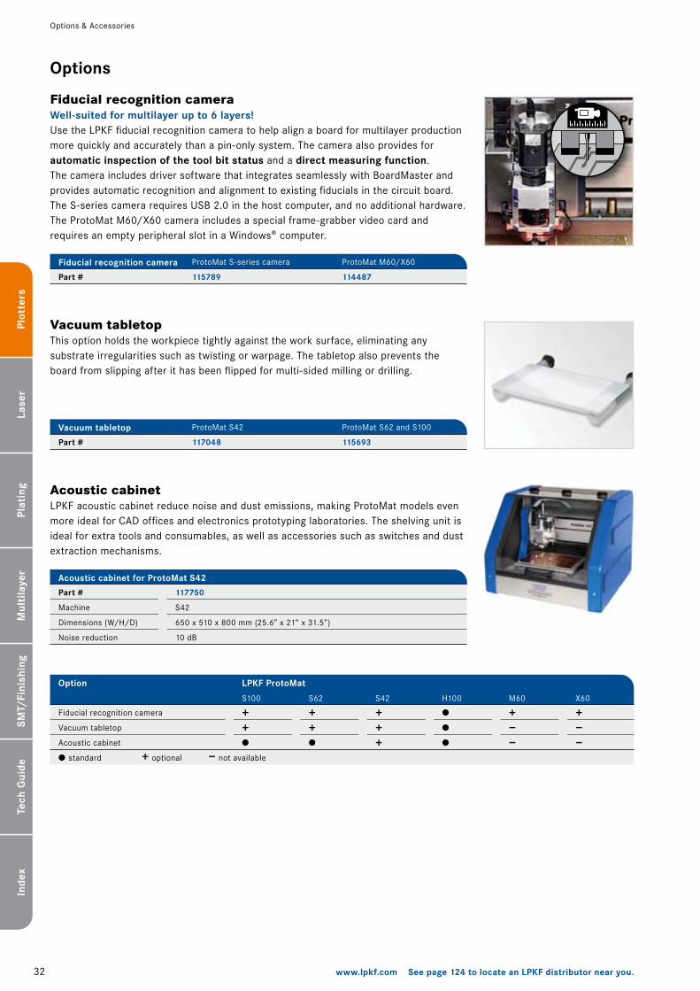
Fiducial recognition camera
Fiducial recognition cameraWell-suited for multilayer up to 6 layers!Use the LPKF fiducial recognition camera to help align a board for multilayer production more quickly and accurately than a pin-only system. The camera also provides for automatic inspection of the tool bit status and a direct measuring function. The camera includes driver software that integrates seamlessly with BoardMaster and provides automatic recognition and alignment to existing fiducials in the circuit board. The S-series camera requires USB �.0 in the host computer, and no additional hardware. The ProtoMat M60/X60 camera includes a special frame-grabber video card and requires an empty peripheral slot in a Windows® computer.
Fiducial recognition camera
Vacuum tabletop
Acoustic cabinet
S�00
LPKF ProtoMatOption
S6� S4� H�00 M60
ProtoMat S-series camera
115789
ProtoMat M60/X60
114487Part #
Vacuum tabletopThis option holds the workpiece tightly against the work surface, eliminating any substrate irregularities such as twisting or warpage. The tabletop also prevents the board from slipping after it has been flipped for multi-sided milling or drilling.
ProtoMat S4�
117048
ProtoMat S6� and S�00
115693
Acoustic cabinetLPKF acoustic cabinet reduce noise and dust emissions, making ProtoMat models even more ideal for CAD offices and electronics prototyping laboratories. The shelving unit is ideal for extra tools and consumables, as well as accessories such as switches and dust extraction mechanisms.
117750
S4�
650 x 5�0 x 800 mm (�5.6” x ��” x 3�.5”)
�0 dB
Part #
Machine
Dimensions (W/H/D)
Noise reduction
Vacuum tabletop
Part #
Acoustic cabinet for ProtoMat S42
X60
++
standard
++
+++
+––
+ optional – not available
+––
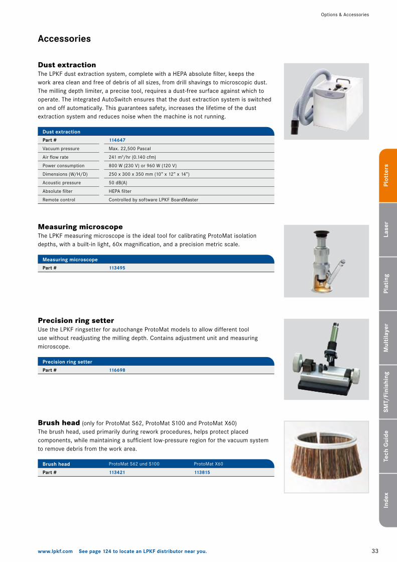
33www.lpkf.com See page 124 to locate an LPKF distributor near you.
Plot
ters
Lase
rPl
atin
gSM
T/Fi
nish
ing
Tech
Gui
deIn
dex
Mul
tila
yer
Accessories
Options & Accessories
Dust extraction
Dust extractionThe LPKF dust extraction system, complete with a HEPA absolute filter, keeps the work area clean and free of debris of all sizes, from drill shavings to microscopic dust. The milling depth limiter, a precise tool, requires a dust-free surface against which to operate. The integrated AutoSwitch ensures that the dust extraction system is switched on and off automatically. This guarantees safety, increases the lifetime of the dust extraction system and reduces noise when the machine is not running.
114647
Max. ��,500 Pascal
�4� m3/hr (0.�40 cfm)
800 W (�30 V) or 960 W (��0 V)
�50 x 300 x 350 mm (�0” x ��” x �4”)
50 dB(A)
HEPA filter
Controlled by software LPKF BoardMaster
Part #
Vacuum pressure
Air flow rate
Power consumption
Dimensions (W/H/D)
Acoustic pressure
Absolute filter
Remote control
Measuring microscopeThe LPKF measuring microscope is the ideal tool for calibrating ProtoMat isolation depths, with a built-in light, 60x magnification, and a precision metric scale.
113495Part #
Precision ring setterUse the LPKF ringsetter for autochange ProtoMat models to allow different tool use without readjusting the milling depth. Contains adjustment unit and measuring microscope.
116698Part #
Brush head (only for ProtoMat S6�, ProtoMat S�00 and ProtoMat X60)The brush head, used primarily during rework procedures, helps protect placed components, while maintaining a sufficient low-pressure region for the vacuum system to remove debris from the work area.
Part #
Measuring microscope
Precision ring setter
Brush head
113421
ProtoMat S6� und S�00 ProtoMat X60
113815
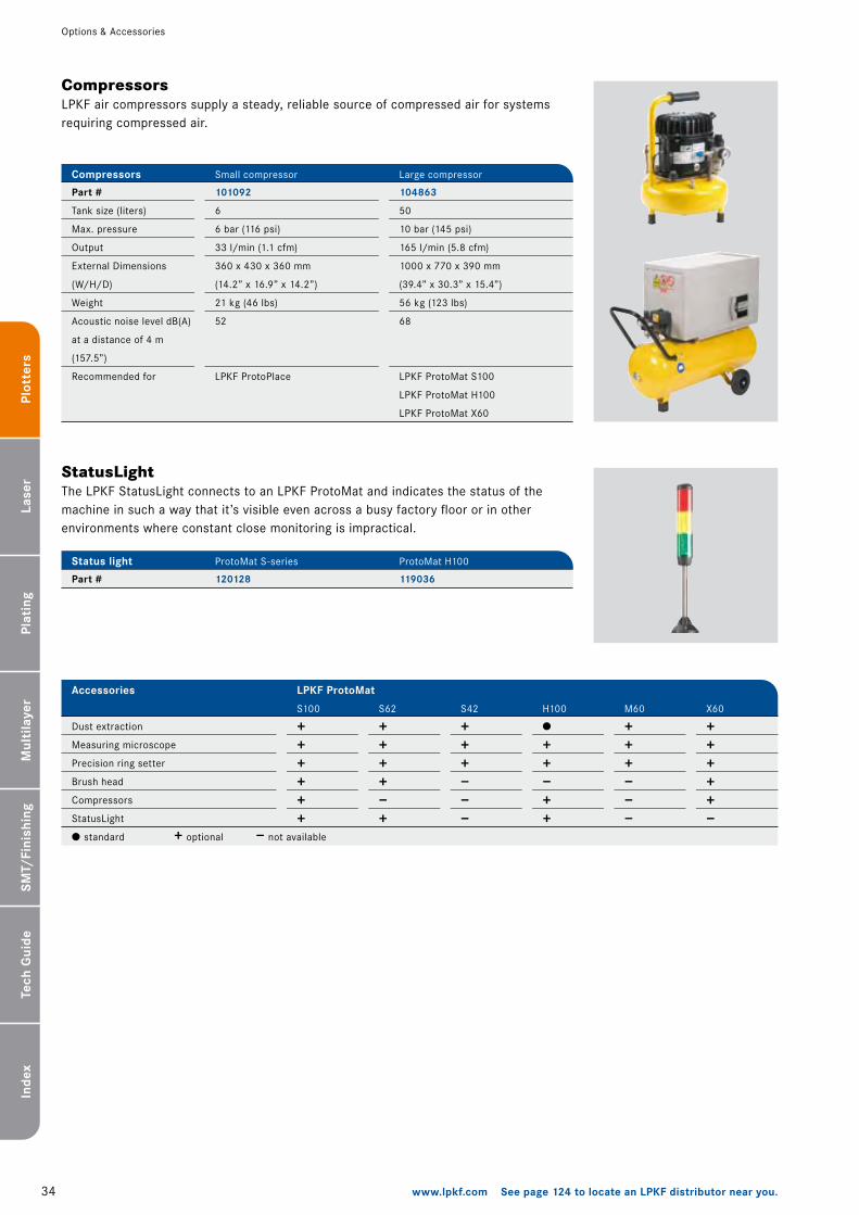
34 www.lpkf.com See page 124 to locate an LPKF distributor near you.
Plot
ters
Lase
rPl
atin
gSM
T/Fi
nish
ing
Tech
Gui
deIn
dex
Mul
tila
yer
Options & Accessories
Small compressor
101092
6
6 bar (��6 psi)
33 l/min (�.� cfm)
360 x 430 x 360 mm
(�4.�” x �6.9” x �4.�”)
�� kg (46 lbs)
5�
LPKF ProtoPlace
CompressorsLPKF air compressors supply a steady, reliable source of compressed air for systems requiring compressed air.
Large compressor
104863
50
�0 bar (�45 psi)
�65 l/min (5.8 cfm)
�000 x 770 x 390 mm
(39.4” x 30.3” x �5.4”)
56 kg (��3 lbs)
68
LPKF ProtoMat S�00
LPKF ProtoMat H�00
LPKF ProtoMat X60
Part #
Tank size (liters)
Max. pressure
Output
External Dimensions
(W/H/D)
Weight
Acoustic noise level dB(A)
at a distance of 4 m
(�57.5”)
Recommended for
StatusLightThe LPKF StatusLight connects to an LPKF ProtoMat and indicates the status of the machine in such a way that it’s visible even across a busy factory floor or in other environments where constant close monitoring is impractical.
120128Part #
Dust extraction
Measuring microscope
Precision ring setter
Brush head
Compressors
StatusLight
S�00
LPKF ProtoMatAccessories
S6� S4� H�00 M60
Compressors
Status light ProtoMat S-series
119036
ProtoMat H�00
X60
standard + optional – not available
++++++
++++–+
+++–––
++–++
+++–––
+++++–
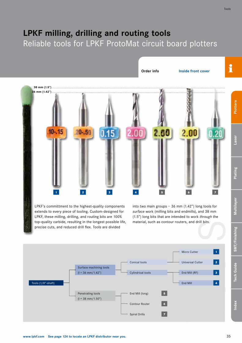
Tool
s
35www.lpkf.com See page 124 to locate an LPKF distributor near you.
Plot
ters
Lase
rPl
atin
gSM
T/Fi
nish
ing
Tech
Gui
deIn
dex
Mul
tila
yer
Tools
LPKF’s committment to the highest-quality components extends to every piece of tooling. Custom-designed for LPKF, these milling, drilling, and routing bits are �00% top-quality carbide, resulting in the longest possible life, precise cuts, and reduced drill flex. Tools are divided
Tools (�/8”-shaft)
Surface machining tools
(l = 36 mm/�.4�”)
Penetrating tools
(l = 38 mm/�.50”)
Conical tools
Cylindrical tools
End Mill (long)
Contour Router
Spiral Drills
End Mill (RF)
End Mill
Micro Cutter
Universal Cutter
1 2 3 4 5 6 7
into two main groups – 36 mm (�.4�”) long tools for surface work (milling bits and endmills), and 38 mm (�.5”) long bits that are intended to work through the material, such as contour routers, and drill bits.
7
6
5
4
3
2
1
38 mm (1.5”)36 mm (1.42”)
Order info Inside front cover
LPKF milling, drilling and routing toolsReliable tools for LPKF ProtoMat circuit board plotters
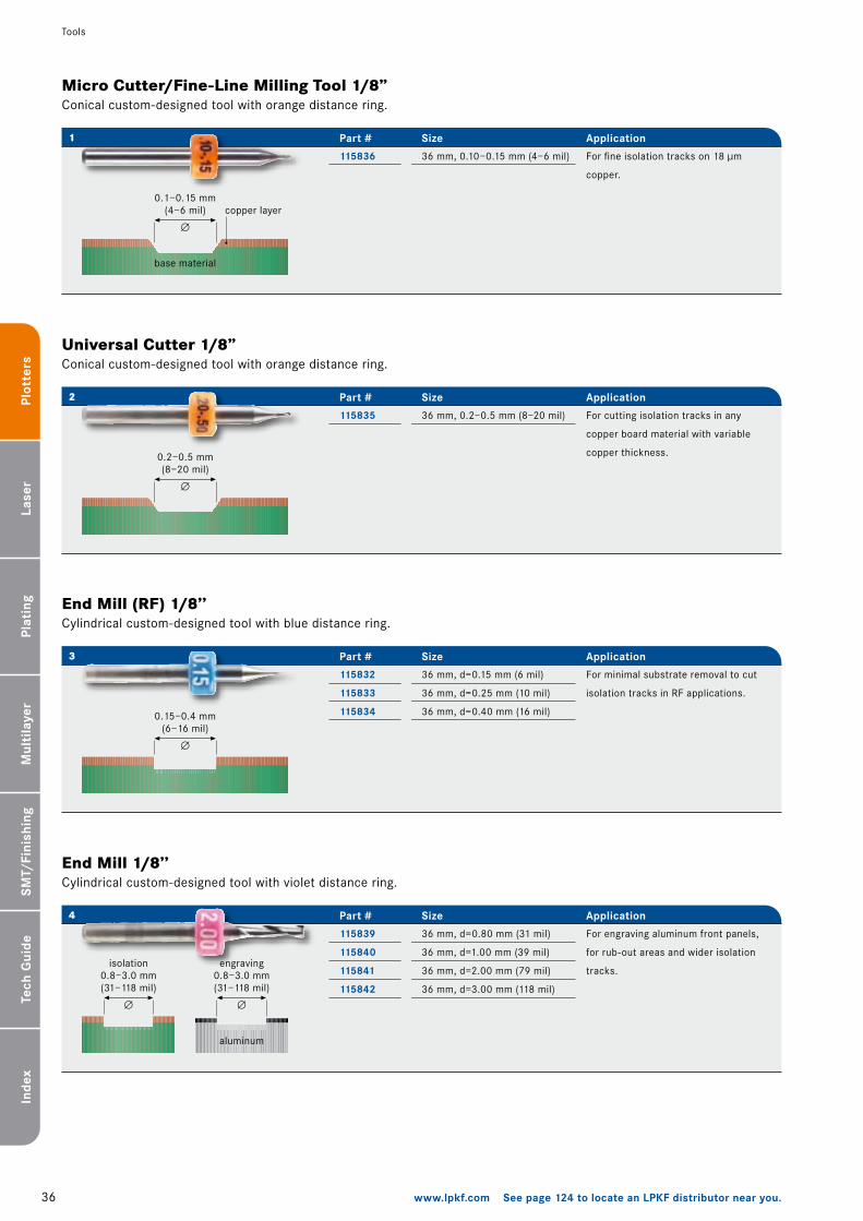
0.2–0.5 mm(8–20 mil)
∅
base material
0.1–0.15 mm(4–6 mil)
∅copper layer
base material
0.15–0.4 mm(6–16 mil)
∅
isolation0.8–3.0 mm(31–118 mil)
∅
aluminum
engraving0.8–3.0 mm(31–118 mil)
∅
36 www.lpkf.com See page 124 to locate an LPKF distributor near you.
Plot
ters
Lase
rPl
atin
gSM
T/Fi
nish
ing
Tech
Gui
deIn
dex
Mul
tila
yer
Tools
115835 36 mm, 0.�–0.5 mm (8–�0 mil)
Size Application
For cutting isolation tracks in any
copper board material with variable
copper thickness.
Part #
Universal Cutter 1/8”Conical custom-designed tool with orange distance ring.
Micro Cutter/Fine-Line Milling Tool 1/8”Conical custom-designed tool with orange distance ring.
115836 36 mm, 0.�0–0.�5 mm (4–6 mil)
Size Application
For fine isolation tracks on �8 µm
copper.
Part #
End Mill (RF) 1/8’’Cylindrical custom-designed tool with blue distance ring.
115832
115833
115834
36 mm, d=0.�5 mm (6 mil)
36 mm, d=0.�5 mm (�0 mil)
36 mm, d=0.40 mm (�6 mil)
Size Application
For minimal substrate removal to cut
isolation tracks in RF applications.
Part #
1
2
3
End Mill 1/8’’Cylindrical custom-designed tool with violet distance ring.
115839
115840
115841
115842
36 mm, d=0.80 mm (3� mil)
36 mm, d=�.00 mm (39 mil)
36 mm, d=�.00 mm (79 mil)
36 mm, d=3.00 mm (��8 mil)
Size Application
For engraving aluminum front panels,
for rub-out areas and wider isolation
tracks.
Part #4
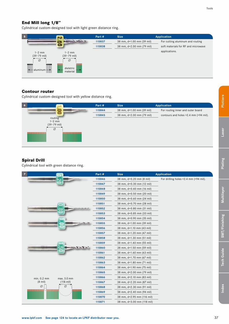
min. 0.2 mm(8 mil)
∅
max. 3.0 mm(118 mil)
∅
1–2 mm(39–79 mil)
∅
1–2 mm(39–79 mil)
∅
dieletricmaterialaluminum
routing1–2 mm
(39–79 mil)
∅
37www.lpkf.com See page 124 to locate an LPKF distributor near you.
Plot
ters
Lase
rPl
atin
gSM
T/Fi
nish
ing
Tech
Gui
deIn
dex
Mul
tila
yer
Tools
End Mill long 1/8’’Cylindrical custom-designed tool with light green distance ring.
115837
115838
38 mm, d=�.00 mm (39 mil)
38 mm, d=�.00 mm (79 mil)
Size Application
For cutting aluminum and routing
soft materials for RF and microwave
applications.
Part #
115844
115845
38 mm, d=�.00 mm (39 mil)
38 mm, d=�.00 mm (79 mil)
SizePart #
Contour routerCylindrical custom-designed tool with yellow distance ring.
Application
For routing inner and outer board
contours and holes >�.4 mm (>94 mil).
Spiral DrillCylindrical tool with green distance ring.
115846
115847
115848
115849
115850
115851
115852
115853
115854
115855
115856
115857
115858
115859
115860
115861
115862
115863
115864
115865
115866
115867
115868
115869
115870
115871
38 mm, d=0.�0 mm (8 mil)
38 mm, d=0.30 mm (�� mil)
38 mm, d=0.40 mm (�6 mil)
38 mm, d=0.50 mm (�0 mil)
38 mm, d=0.60 mm (�4 mil)
38 mm, d=0.70 mm (�8 mil)
38 mm, d=0.80 mm (3� mil)
38 mm, d=0.85 mm (33 mil)
38 mm, d=0.90 mm (35 mil)
38 mm, d=�.00 mm (39 mil)
38 mm, d=�.�0 mm (43 mil)
38 mm, d=�.�0 mm (47 mil)
38 mm, d=�.30 mm (5� mil)
38 mm, d=�.40 mm (55 mil)
38 mm, d=�.50 mm (59 mil)
38 mm, d=�.60 mm (63 mil)
38 mm, d=�.70 mm (67 mil)
38 mm, d=�.80 mm (7� mil)
38 mm, d=�.90 mm (75 mil)
38 mm, d=�.00 mm (79 mil)
38 mm, d=�.�0 mm (83 mil)
38 mm, d=�.�0 mm (87 mil)
38 mm, d=�.30 mm (9� mil)
38 mm, d=�.40 mm (94 mil)
38 mm, d=�.95 mm (��6 mil)
38 mm, d=3.00 mm (��8 mil)
Size Application
For drilling holes <�.4 mm (<94 mil).
Part #
6
7
5
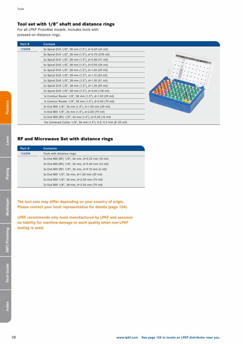
38 www.lpkf.com See page 124 to locate an LPKF distributor near you.
Plot
ters
Lase
rPl
atin
gSM
T/Fi
nish
ing
Tech
Gui
deIn
dex
Mul
tila
yer
Tools
115909 5x Spiral Drill �/8”, 38 mm (�.5”), d=0.60 (�4 mil)
5x Spiral Drill �/8”, 38 mm (�.5”), d=0.70 (�78 mil)
5x Spiral Drill �/8”, 38 mm (�.5”), d=0.80 (3� mil)
5x Spiral Drill �/8”, 38 mm (�.5”), d=0.90 (35 mil)
5x Spiral Drill �/8”, 38 mm (�.5”), d=�.00 (39 mil)
�x Spiral Drill �/8”, 38 mm (�.5”), d=�.�0 (43 mil)
�x Spiral Drill �/8”, 38 mm (�.5”), d=�.30 (5� mil)
�x Spiral Drill �/8”, 38 mm (�.5”), d=�.50 (59 mil)
�x Spiral Drill �/8”, 38 mm (�.5”), d=3.00 (��8 mil)
�x Contour Router �/8”, 38 mm (�.5”), d=�.00 (39 mil)
�x Contour Router �/8”, 38 mm (�.5”), d=�.00 (79 mil)
�x End Mill �/8”, 36 mm (�.4”), d=�.00 mm (39 mil)
�x End Mill �/8”, 36 mm (�.4”), d=�.00 (79 mil)
�x End Mill (RF) �/8”, 36 mm (�.4”), d=0.40 (�6 mil)
�0x Universal Cutter �/8”, 36 mm (�.4”), 0.�–0.5 mm (8–�0 mil)
ContentPart #
Tool set with 1/8” shaft and distance ringsFor all LPKF ProtoMat models. Includes tools with pressed-on distance rings.
116394
Contents
Tools with distance rings:
5x End Mill (RF) �/8”, 36 mm, d=0.�5 mm (�0 mil)
3x End Mill (RF) �/8”, 36 mm, d=0.40 mm (�6 mil)
3x End Mill (RF) �/8”, 36 mm, d=0.�5 mm (6 mil)
5x End Mill �/8”, 36 mm, d=�.00 mm (39 mil)
�x End Mill �/8”, 36 mm, d=�.00 mm (79 mil)
�x End Mill �/8”, 38 mm, d=�.00 mm (79 mil)
Part #
RF and Microwave Set with distance rings
The tool sets may differ depending on your country of origin. Please contact your local representative for details (page 124).
LPKF recommends only tools manufactured by LPKF and assumes no liability for machine damage or work quality when non-LPKF tooling is used.
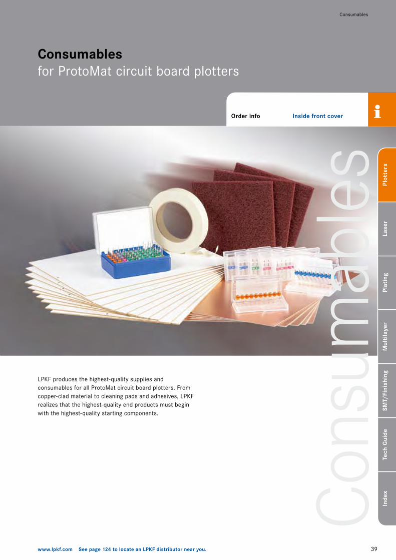
Con
sum
able
s
39www.lpkf.com See page 124 to locate an LPKF distributor near you.
Plot
ters
Lase
rPl
atin
gSM
T/Fi
nish
ing
Tech
Gui
deIn
dex
Mul
tila
yer
Consumables
LPKF produces the highest-quality supplies and consumables for all ProtoMat circuit board plotters. From copper-clad material to cleaning pads and adhesives, LPKF realizes that the highest-quality end products must begin with the highest-quality starting components.
Order info Inside front cover
Consumablesfor ProtoMat circuit board plotters
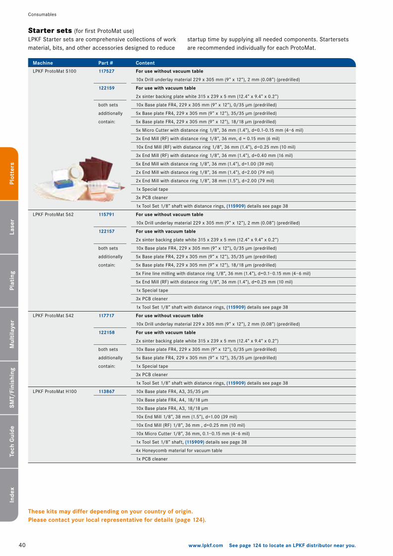
40 www.lpkf.com See page 124 to locate an LPKF distributor near you.
Plot
ters
Lase
rPl
atin
gSM
T/Fi
nish
ing
Tech
Gui
deIn
dex
Mul
tila
yer
Consumables
LPKF Starter sets are comprehensive collections of work material, bits, and other accessories designed to reduce
117527
122159
115791
122157
117717
122158
113867
For use without vacuum table
�0x Drill underlay material ��9 x 305 mm (9” x ��”), � mm (0.08”) (predrilled)
For use with vacuum table
�x sinter backing plate white 3�5 x �39 x 5 mm (��.4” x 9.4” x 0.�”)
�0x Base plate FR4, ��9 x 305 mm (9” x ��”), 0/35 µm (predrilled)
5x Base plate FR4, ��9 x 305 mm (9” x ��”), 35/35 µm (predrilled)
5x Base plate FR4, ��9 x 305 mm (9” x ��”), �8/�8 µm (predrilled)
5x Micro Cutter with distance ring �/8”, 36 mm (�.4”), d=0.�-0.�5 mm (4–6 mil)
3x End Mill (RF) with distance ring �/8”, 36 mm, d = 0.�5 mm (6 mil)
�0x End Mill (RF) with distance ring �/8”, 36 mm (�.4”), d=0.�5 mm (�0 mil)
3x End Mill (RF) with distance ring �/8”, 36 mm (�.4”), d=0.40 mm (�6 mil)
5x End Mill with distance ring �/8”, 36 mm (�.4”), d=�.00 (39 mil)
�x End Mill with distance ring �/8”, 36 mm (�.4”), d=�.00 (79 mil)
�x End Mill with distance ring �/8”, 38 mm (�.5”), d=�.00 (79 mil)
�x Special tape
3x PCB cleaner
�x Tool Set �/8” shaft with distance rings, (115909) details see page 38
For use without vacuum table
�0x Drill underlay material ��9 x 305 mm (9” x ��”), � mm (0.08”) (predrilled)
For use with vacuum table
�x sinter backing plate white 3�5 x �39 x 5 mm (��.4” x 9.4” x 0.�”)
�0x Base plate FR4, ��9 x 305 mm (9” x ��”), 0/35 µm (predrilled)
5x Base plate FR4, ��9 x 305 mm (9” x ��”), 35/35 µm (predrilled)
5x Base plate FR4, ��9 x 305 mm (9” x ��”), �8/�8 µm (predrilled)
5x Fine line milling with distance ring �/8”, 36 mm (�.4”), d=0.�–0.�5 mm (4–6 mil)
5x End Mill (RF) with distance ring �/8”, 36 mm (�.4”), d=0.�5 mm (�0 mil)
�x Special tape
3x PCB cleaner
�x Tool Set �/8” shaft with distance rings, (115909) details see page 38
For use without vacuum table
�0x Drill underlay material ��9 x 305 mm (9” x ��”), � mm (0.08”) (predrilled)
For use with vacuum table
�x sinter backing plate white 3�5 x �39 x 5 mm (��.4” x 9.4” x 0.�”)
�0x Base plate FR4, ��9 x 305 mm (9” x ��”), 0/35 µm (predrilled)
5x Base plate FR4, ��9 x 305 mm (9” x ��”), 35/35 µm (predrilled)
�x Special tape
3x PCB cleaner
�x Tool Set �/8” shaft with distance rings, (115909) details see page 38
�0x Base plate FR4, A3, 35/35 µm
�0x Base plate FR4, A4, �8/�8 µm
�0x Base plate FR4, A3, �8/�8 µm
�0x End Mill �/8”, 38 mm (�.5”), d=�.00 (39 mil)
�0x End Mill (RF) �/8”, 36 mm , d=0.�5 mm (�0 mil)
�0x Micro Cutter �/8”, 36 mm, 0.�–0.�5 mm (4–6 mil)
�x Tool Set �/8” shaft, (115909) details see page 38
4x Honeycomb material for vacuum table
�x PCB cleaner
ContentPart #
LPKF ProtoMat S�00
LPKF ProtoMat S6�
LPKF ProtoMat S4�
LPKF ProtoMat H�00
Machine
Starter sets (for first ProtoMat use)
These kits may differ depending on your country of origin. Please contact your local representative for details (page 124).
startup time by supplying all needed components. Startersets are recommended individually for each ProtoMat.
both sets
additionally
contain:
both sets
additionally
contain:
both sets
additionally
contain:
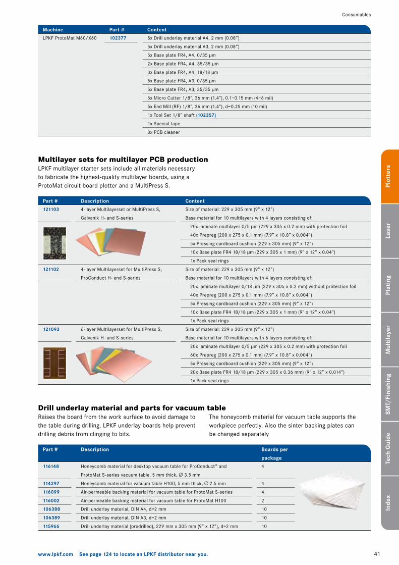
4�www.lpkf.com See page 124 to locate an LPKF distributor near you.
Plot
ters
Lase
rPl
atin
gSM
T/Fi
nish
ing
Tech
Gui
deIn
dex
Mul
tila
yer
Consumables
LPKF multilayer starter sets include all materials necessary to fabricate the highest-quality multilayer boards, using a ProtoMat circuit board plotter and a MultiPress S.
Multilayer sets for multilayer PCB production
116148
114297
116099
116002
106388
106389
115966
Honeycomb material for desktop vacuum table for ProConduct® and
ProtoMat S-series vacuum table, 5 mm thick, 3.5 mm
Honeycomb material for vacuum table H�00, 5 mm thick, �.5 mm
Air-permeable backing material for vacuum table for ProtoMat S-series
Air-permeable backing material for vacuum table for ProtoMat H�00
Drill underlay material, DIN A4, d=� mm
Drill underlay material, DIN A3, d=� mm
Drill underlay material (predrilled), ��9 mm x 305 mm (9” x ��”), d=� mm
DescriptionPart #
4
4
4
�
�0
�0
�0
Boards per
package
Raises the board from the work surface to avoid damage to the table during drilling. LPKF underlay boards help prevent drilling debris from clinging to bits.
The honeycomb material for vacuum table supports the workpiece perfectly. Also the sinter backing plates can be changed separately
Drill underlay material and parts for vacuum table
ContentPart #Machine
102377 5x Drill underlay material A4, � mm (0.08”)
5x Drill underlay material A3, � mm (0.08”)
5x Base plate FR4, A4, 0/35 µm
�x Base plate FR4, A4, 35/35 µm
3x Base plate FR4, A4, �8/�8 µm
5x Base plate FR4, A3, 0/35 µm
5x Base plate FR4, A3, 35/35 µm
5x Micro Cutter �/8”, 36 mm (�.4”), 0.�–0.�5 mm (4–6 mil)
5x End Mill (RF) �/8”, 36 mm (�.4”), d=0.�5 mm (�0 mil)
�x Tool Set �/8” shaft (102357)
�x Special tape
3x PCB cleaner
LPKF ProtoMat M60/X60
121103
121102
121093
Size of material: ��9 x 305 mm (9” x ��”)
Base material for �0 multilayers with 4 layers consisting of:
�0x laminate multilayer 0/5 µm (��9 x 305 x 0.� mm) with protection foil
40x Prepreg (�00 x �75 x 0.� mm) (7.9” x �0.8” x 0.004”)
5x Pressing cardboard cushion (��9 x 305 mm) (9” x ��”)
�0x Base plate FR4 �8/�8 µm (��9 x 305 x � mm) (9” x ��” x 0.04”)
�x Pack seal rings
Size of material: ��9 x 305 mm (9” x ��”)
Base material for �0 multilayers with 4 layers consisting of:
�0x laminate multilayer 0/�8 µm (��9 x 305 x 0.� mm) without protection foil
40x Prepreg (�00 x �75 x 0.� mm) (7.9” x �0.8” x 0.004”)
5x Pressing cardboard cushion (��9 x 305 mm) (9” x ��”)
�0x Base plate FR4 �8/�8 µm (��9 x 305 x � mm) (9” x ��” x 0.04”)
�x Pack seal rings
Size of material: ��9 x 305 mm (9” x ��”)
Base material for �0 multilayers with 6 layers consisting of:
�0x laminate multilayer 0/5 µm (��9 x 305 x 0.� mm) with protection foil
60x Prepreg (�00 x �75 x 0.� mm) (7.9” x �0.8” x 0.004”)
5x Pressing cardboard cushion (��9 x 305 mm) (9” x ��”)
�0x Base plate FR4 �8/�8 µm (��9 x 305 x 0.36 mm) (9” x ��” x 0.0�4”)
�x Pack seal rings
ContentPart #
4-layer Multilayerset or MultiPress S,
Galvanik H- and S-series
4-layer Multilayerset for MultiPress S,
ProConduct H- and S-series
6-layer Multilayerset for MultiPress S,
Galvanik H- and S-series
Description
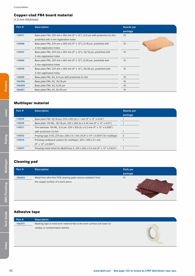
4� www.lpkf.com See page 124 to locate an LPKF distributor near you.
Plot
ters
Lase
rPl
atin
gSM
T/Fi
nish
ing
Tech
Gui
deIn
dex
Mul
tila
yer
Consumables
106403 Metal-free ultra-fine PCB cleaning pads remove oxidation from
the copper surface of a work piece.
DescriptionPart #
106373 Masking tape to hold work material flat to the work surface and leave no
residue or contamination behind.
DescriptionPart #
Cleaning pad
Adhesive tape
Copper-clad FR4 board material(�.5 mm thickness)
115971
115968
115967
115969
115970
112059
106398
106400
106401
Base plate FR4, ��9 mm x 305 mm (9” x ��”), 5/5 µm with protective Cu-foil,
predrilled with 3 mm registration holes
Base plate FR4, ��9 mm x 305 mm (9” x ��”), 0/�8 µm, predrilled with
3 mm registration holes
Base plate FR4, ��9 mm x 305 mm (9” x ��”), �8/�8 µm, predrilled with
3 mm registration holes
Base plate FR4, ��9 mm x 305 mm (9” x ��”), 0/35 µm, predrilled with
3 mm registration holes
Base plate FR4, ��9 mm x 305 mm (9” x ��”), 35/35 µm, predrilled with
3 mm registration holes
Base plate FR4, A3, 5/5 µm with protective Cu-foil
Base plate FR4, A3, �8/�8 µm
Base plate FR4, A3, 0/35 µm
Base plate FR4, A3, 35/35 µm
DescriptionPart #
�0
�0
�0
�0
�0
�0
�0
�0
�0
Boards per
package
Multilayer material
119574
119575
119571
119572
119573
119577
Base plate FR4 �8/�8 µm, ��9 x 305 (k) x � mm (9” x ��” x 0.04”)
Base plate �04 ML, �8/�8 µm, ��9 x 305 (k) x 0.36 mm (9” x ��” x 0.0�”)
Thin laminate �04 ML, 5/0 µm, ��9 x 305 (k) x 0.� mm (9” x ��” x 0.008”)
with protection Cu-foil
Prepreg type ���5, �75 (k) x �00 x 0.� mm (�0.8” x 7.9” x 0.004”) for multilayer
Pressing cardboard cushion for multilayer, ��9 x 305 x 0.� mm
(9” x ��” x 0.004”)
Pressing metal sheet for MultiPress S, ��9 x 305 x 0.4 mm (9” x ��” x 0.0�6”)
�
�
�
�
�
�
DescriptionPart # Boards per
package
�0
Pads per
package
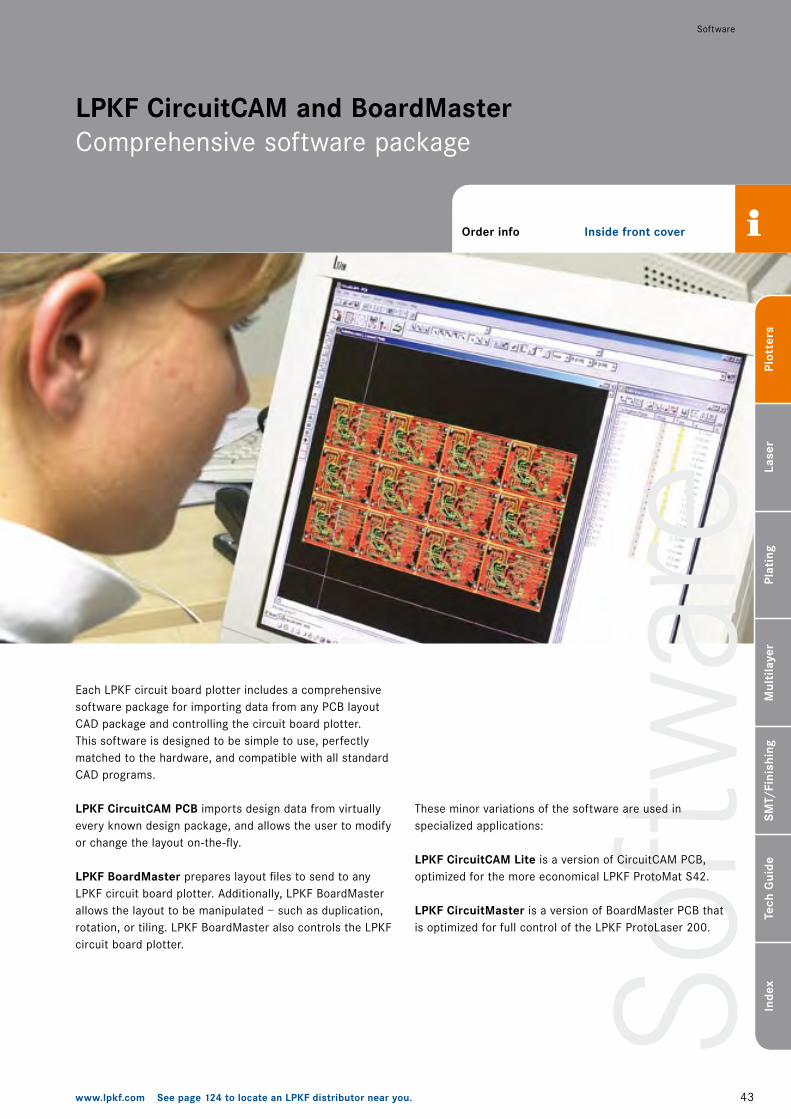
Soft
war
e
43www.lpkf.com See page 124 to locate an LPKF distributor near you.
Plot
ters
Lase
rPl
atin
gSM
T/Fi
nish
ing
Tech
Gui
deIn
dex
Mul
tila
yer
Software
Order info Inside front cover
LPKF CircuitCAM and BoardMaster Comprehensive software package
Each LPKF circuit board plotter includes a comprehensive software package for importing data from any PCB layout CAD package and controlling the circuit board plotter. This software is designed to be simple to use, perfectly matched to the hardware, and compatible with all standard CAD programs.
LPKF CircuitCAM PCB imports design data from virtually every known design package, and allows the user to modify or change the layout on-the-fly.
LPKF BoardMaster prepares layout files to send to any LPKF circuit board plotter. Additionally, LPKF BoardMaster allows the layout to be manipulated – such as duplication, rotation, or tiling. LPKF BoardMaster also controls the LPKF circuit board plotter.
These minor variations of the software are used in specialized applications:
LPKF CircuitCAM Lite is a version of CircuitCAM PCB, optimized for the more economical LPKF ProtoMat S4�.
LPKF CircuitMaster is a version of BoardMaster PCB that is optimized for full control of the LPKF ProtoLaser �00.
44 www.lpkf.com See page 124 to locate an LPKF distributor near you.
Plot
ters
Lase
rPl
atin
gSM
T/Fi
nish
ing
Tech
Gui
deIn
dex
Mul
tila
yer
Software
Import formats
Supported shapes
Export formats
Editing functions
Special functions
Display functions
Marker functions
Graphic functions
Control functions
Insulation methods
Insulation tools
Languages
Hard-/software requirements
Supplied with
Gerber Standard (RS-�74-D), Extended Gerber
(RS-�74-X), Excellon NC Drill (version � and �),
Sieb & Meier NC Drill, HP-GL™
LPKF BoardMaster (LMD)
Contour routing path generator with breakout tabs
Measuring
�–� tools
LPKF ProtoMat S4� *
LPKF CircuitCAM LITE
Specification table
LPKF CircuitCAM PCB
Gerber Standard (RS-�74-D), Extended Gerber
(RS-�74-X), Excellon NC Drill (version � and �),
Sieb & Meier NC Drill, HP-GL™, Barco® DPF,
AutoCAD™ DXF, ODB ++®
LPKF BoardMaster (LMD), Gerber Standard
(RS-�74-D), Gerber Extended (RS-�74-X), Excellon
NC Drill, HP-GL™, DXF
Routing path generator with breakout tabs, volume
operations, joining/separating objects, step &
repeat (multiple PCB), polygon cut-out, ground plane
generation with defined clearance, batch functions
Measuring, design rule check
�–4 tools
LPKF ProtoMat S6�, S�00, H�00, M60, X60
and ProtoLaser �00
Circle, square, rectangle (also rounded or angled), octagon, oval, marker, IEC ��8� (�000–�0�4) including
thermal reliefs, fiducials, etc., special (arbitrary definable)
Original modification, relocating, duplicating, rotating, mirroring, erasing, extending/severing lines, line/path
extension/shortening, line path/segment parallel shifting, line path/object polygon conversion (Fill), curve
linking/closing
Zoom window (freely definable), zoom in/out, overview, redraw, individual layers selectable/visible, panning
(keyboard), layer in solid/outline/center line display, �6 pre-set colors (up to �6 million freely available),
different colors for tracks and pads of the same layer, different colors for insulation tools
Single element, total layer, all layers, pad groups, selection and limiting to specific layers possible for lines/
polygons/circles/rectangles/pads/holes (multiple choice and restriction to specific layers possible)
Lines (open/closed), circle, polygon, rectangle, pad, hole, text (TTF, TTC)
Single insulation method, additional multiple insulation of pads, removal of residual copper spikes (spike
option), milling out of large insulation areas (rub-out), concentric or in serpentines maintaining minimum
insulation spaces, zone insulation (only PCB version), inverse insulation
Microsoft® Windows® �000/XP, �.� GHz processor or better, min. 5�� MB RAM, screen resolution min. XGA
English, German, French, Spanish, Japanese and Chinese
* Upgrade from LITE to PCB available. Specifications subject to change.
LPKF CircuitCAM – the software interface to your CAD/EDA system
Simple and functionalA software wizard guides even inexperienced users through the program sequence step-by-step, from data import, through path generation, to the export of production data. LPKF CircuitCAM processes the same data and data files required by a commercial board fabricator. CircuitCAM automatically imports aperture tables and tool lists, followed by Gerber and NC drilling files:
Data import: Imports Gerber®, GerberX, HP-GL™, Excellon®, Sieb & Meier, DXF, Barco®, ODB++® Data export: Exports Gerber®, GerberX, HP-GL™, LMD, Excellon®, DXF formats Intelligent insulation: This process guarantees removal of copper using various automatic and individually adjustable insulation options, reducing milling time and increasing tool life, with up to four different tools per insulation strategy and freely definable rub-outs – including polygons.
Design rule check: Checks track/gap spaces. Auto contour routing: Automatically generates routing paths with definable breakout tabs. Auto ground plane: Automatically generates ground planes. Direct drawing input: Draws simple front panels or printed circuit boards. Editing directly: For example, modifying line-widths, changing hole diameters, shifting holes, adding copper areas, etc. Software wizard: Integrated program assistant guides the user and reduces the learning curve. True type fonts: CircuitCAM understands TTF and TTC during text functions. Auto assign: Automatically assigns production phases/tools for BoardMaster. Machining order control: Modifies cutting direction and sequence.
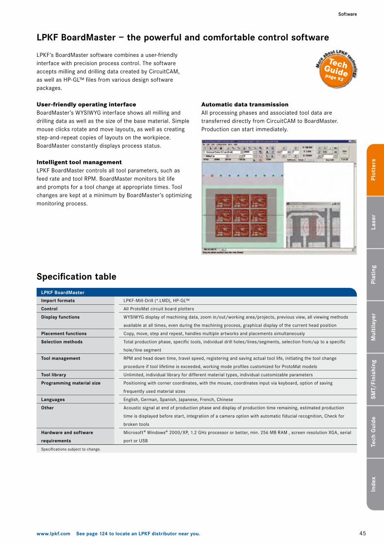
45www.lpkf.com See page 124 to locate an LPKF distributor near you.
Plot
ters
Lase
rPl
atin
gSM
T/Fi
nish
ing
Tech
Gui
deIn
dex
Mul
tila
yer
SoftwareSoftware
Import formats
Control
Display functions
Placement functions
Selection methods
Tool management
Tool library
Programming material size
Languages
Other
Hardware and software
requirements
LPKF-Mill-Drill (*.LMD), HP-GL™
All ProtoMat circuit board plotters
WYSIWYG display of machining data, zoom in/out/working area/projects, previous view, all viewing methods
available at all times, even during the machining process, graphical display of the current head position
Copy, move, step and repeat, handles multiple artworks and placements simultaneously
Total production phase, specific tools, individual drill holes/lines/segments, selection from/up to a specific
hole/line segment
RPM and head down time, travel speed, registering and saving actual tool life, initiating the tool change
procedure if tool lifetime is exceeded, working mode profiles customized for ProtoMat models
Unlimited, individual library for different material types, individual customizable parameters
Positioning with corner coordinates, with the mouse, coordinates input via keyboard, option of saving
frequently used material sizes
English, German, Spanish, Japanese, French, Chinese
Acoustic signal at end of production phase and display of production time remaining, estimated production
time is displayed before start, integration of a camera option with automatic fiducial recognition, Check for
broken tools
Microsoft® Windows® �000/XP, �.� GHz processor or better, min. �56 MB RAM , screen resolution XGA, serial
port or USB
LPKF BoardMaster
LPKF BoardMaster – the powerful and comfortable control software
LPKF’s BoardMaster software combines a user-friendly interface with precision process control. The software accepts milling and drilling data created by CircuitCAM, as well as HP-GL™ files from various design software packages.
User-friendly operating interfaceBoardMaster’s WYSIWYG interface shows all milling and drilling data as well as the size of the base material. Simple mouse clicks rotate and move layouts, as well as creating step-and-repeat copies of layouts on the workpiece. BoardMaster constantly displays process status.
Intelligent tool managementLPKF BoardMaster controls all tool parameters, such as feed rate and tool RPM. BoardMaster monitors bit life and prompts for a tool change at appropriate times. Tool changes are kept at a minimum by BoardMaster’s optimizing monitoring process.
Automatic data transmissionAll processing phases and associated tool data are transferred directly from CircuitCAM to BoardMaster. Production can start immediately.
Specifications subject to change.
Specification table
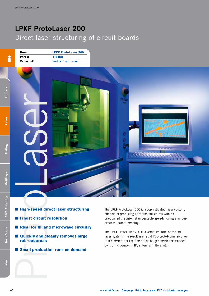
Prot
oLas
er
46 www.lpkf.com See page 124 to locate an LPKF distributor near you.
Plot
ters
Lase
rPl
atin
gSM
T/Fi
nish
ing
Tech
Gui
deIn
dex
Mul
tila
yer
LPKF ProtoLaser 200 Direct laser structuring of circuit boards
Item LPKF ProtoLaser 200Part # 118188Order info Inside front cover
The LPKF ProtoLaser �00 is a sophisticated laser system, capable of producing ultra-fine structures with an unequalled precision at unbeatable speeds, using a unique process (patent pending).
The LPKF ProtoLaser �00 is a versatile state-of-the-art laser system. The result is a rapid PCB prototyping solution that’s perfect for the fine precision geometries demanded by RF, microwave, RFID, antennas, filters, etc.
High-speed direct laser structuring
Finest circuit resolution
Ideal for RF and microwave circuitry
Quickly and cleanly removes large rub-out areas
Small production runs on demand
LPKF ProtoLaser �00
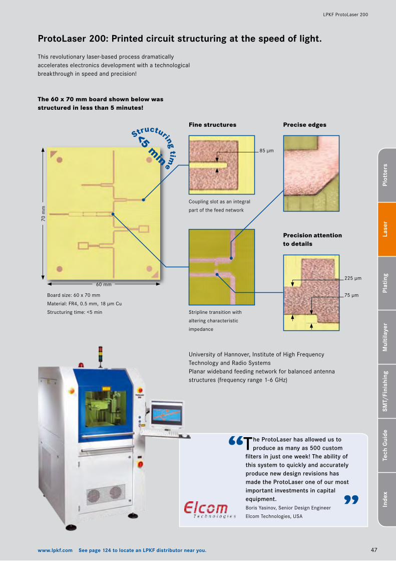
47www.lpkf.com See page 124 to locate an LPKF distributor near you.
Plot
ters
Lase
rPl
atin
gSM
T/Fi
nish
ing
Tech
Gui
deIn
dex
Mul
tila
yer
LPKF ProtoLaser �00
This revolutionary laser-based process dramatically accelerates electronics development with a technological breakthrough in speed and precision!
University of Hannover, Institute of High Frequency Technology and Radio SystemsPlanar wideband feeding network for balanced antenna structures (frequency range �-6 GHz)
Board size: 60 x 70 mm
Material: FR4, 0.5 mm, �8 µm Cu
Structuring time: <5 min Stripline transition with
altering characteristic
impedance
Coupling slot as an integral
part of the feed network
85 µm
��5 µm
75 µm
The ProtoLaser has allowed us to produce as many as 500 custom
filters in just one week! The ability of this system to quickly and accurately produce new design revisions has made the ProtoLaser one of our most important investments in capital equipment.Boris Yasinov, Senior Design Engineer
Elcom Technologies, USA
“
”
Precision attention to details
Precise edgesFine structures
The 60 x 70 mm board shown below was structured in less than 5 minutes!
Structuring time
<5 min
60 mm
70 m
mProtoLaser 200: Printed circuit structuring at the speed of light.
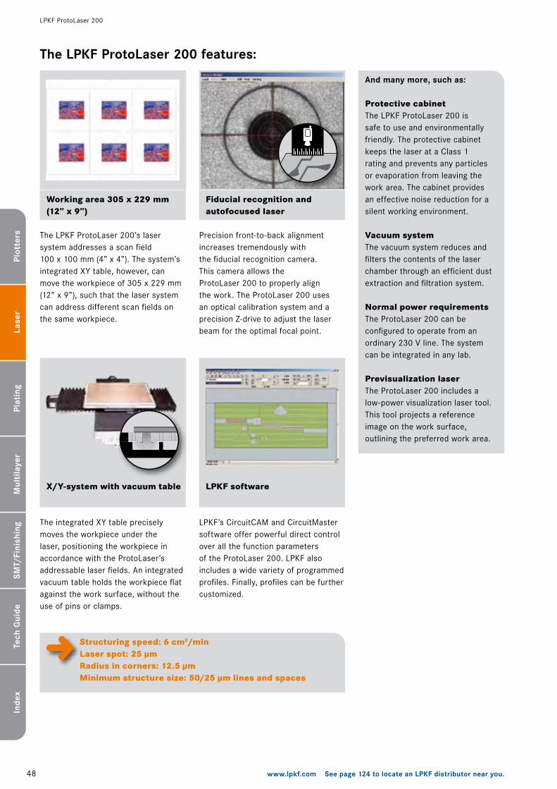
48 www.lpkf.com See page 124 to locate an LPKF distributor near you.
Plot
ters
Lase
rPl
atin
gSM
T/Fi
nish
ing
Tech
Gui
deIn
dex
Mul
tila
yer
LPKF ProtoLaser �00
Working area 305 x 229 mm (12” x 9”)
The LPKF ProtoLaser �00’s laser system addresses a scan field �00 x �00 mm (4” x 4”). The system’s integrated XY table, however, can move the workpiece of 305 x ��9 mm (��” x 9”), such that the laser system can address different scan fields on the same workpiece.
Protective cabinetThe LPKF ProtoLaser �00 is safe to use and environmentally friendly. The protective cabinet keeps the laser at a Class � rating and prevents any particles or evaporation from leaving the work area. The cabinet provides an effective noise reduction for a silent working environment.
Fiducial recognition and autofocused laser
Precision front-to-back alignment increases tremendously with the fiducial recognition camera. This camera allows the ProtoLaser �00 to properly align the work. The ProtoLaser �00 uses an optical calibration system and a precision Z-drive to adjust the laser beam for the optimal focal point.
X/Y-system with vacuum table
The integrated XY table precisely moves the workpiece under the laser, positioning the workpiece in accordance with the ProtoLaser’s addressable laser fields. An integrated vacuum table holds the workpiece flat against the work surface, without the use of pins or clamps.
And many more, such as:
The LPKF ProtoLaser 200 features:
Vacuum systemThe vacuum system reduces and filters the contents of the laser chamber through an efficient dust extraction and filtration system.
Normal power requirementsThe ProtoLaser �00 can be configured to operate from an ordinary �30 V line. The system can be integrated in any lab.
Previsualization laserThe ProtoLaser �00 includes a low-power visualization laser tool. This tool projects a reference image on the work surface, outlining the preferred work area.
LPKF software
LPKF’s CircuitCAM and CircuitMaster software offer powerful direct control over all the function parameters of the ProtoLaser �00. LPKF also includes a wide variety of programmed profiles. Finally, profiles can be further customized.
Structuring speed: 6 cm2/minLaser spot: 25 µmRadius in corners: 12.5 µmMinimum structure size: 50/25 µm lines and spaces
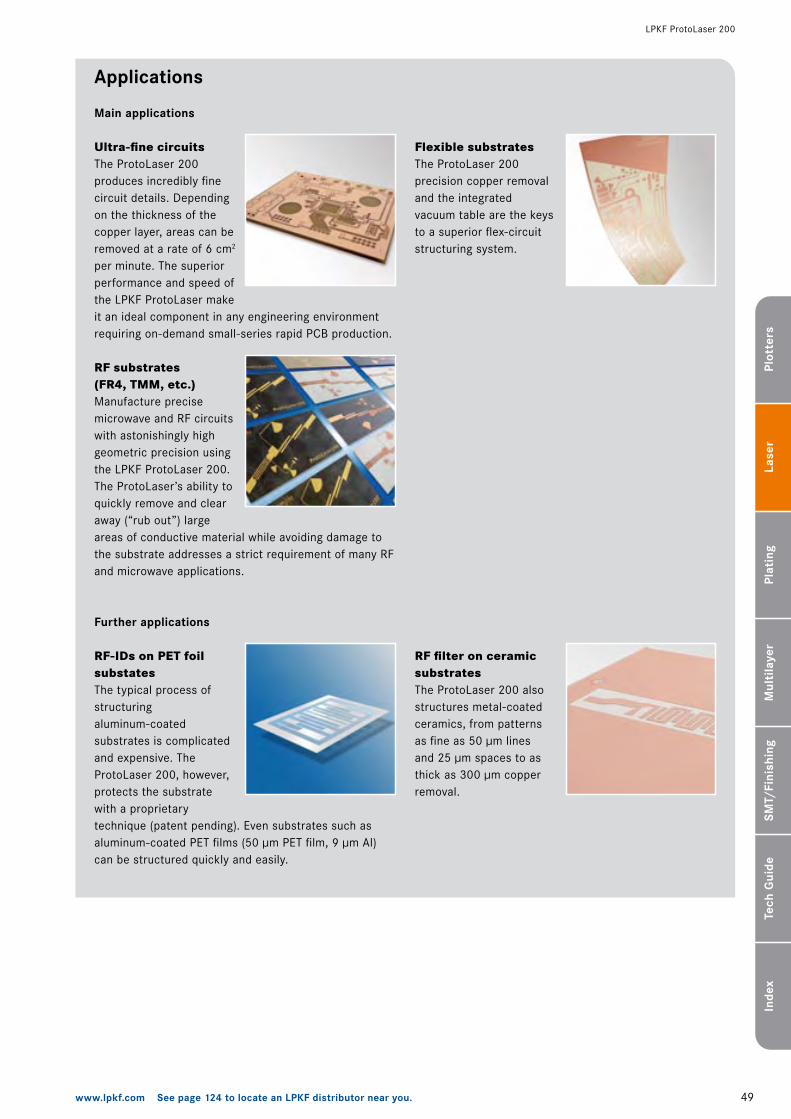
49www.lpkf.com See page 124 to locate an LPKF distributor near you.
Plot
ters
Lase
rPl
atin
gSM
T/Fi
nish
ing
Tech
Gui
deIn
dex
Mul
tila
yer
LPKF ProtoLaser �00
Main applications
Applications
RF filter on ceramic substratesThe ProtoLaser �00 also structures metal-coated ceramics, from patterns as fine as 50 µm lines and �5 µm spaces to as thick as 300 µm copper removal.
Ultra-fine circuitsThe ProtoLaser �00 produces incredibly fine circuit details. Depending on the thickness of the copper layer, areas can be removed at a rate of 6 cm� per minute. The superior performance and speed of the LPKF ProtoLaser make it an ideal component in any engineering environment requiring on-demand small-series rapid PCB production.
RF-IDs on PET foil substatesThe typical process of structuring aluminum-coated substrates is complicated and expensive. The ProtoLaser �00, however, protects the substrate with a proprietary technique (patent pending). Even substrates such as aluminum-coated PET films (50 µm PET film, 9 µm Al) can be structured quickly and easily.
Flexible substratesThe ProtoLaser �00 precision copper removal and the integrated vacuum table are the keys to a superior flex-circuit structuring system.
RF substrates (FR4, TMM, etc.)Manufacture precise microwave and RF circuits with astonishingly high geometric precision using the LPKF ProtoLaser �00. The ProtoLaser’s ability to quickly remove and clear away (“rub out”) large areas of conductive material while avoiding damage to the substrate addresses a strict requirement of many RF and microwave applications.
Further applications
50 www.lpkf.com See page 124 to locate an LPKF distributor near you.
Plot
ters
Lase
rPl
atin
gSM
T/Fi
nish
ing
Tech
Gui
deIn
dex
Mul
tila
yer
Part #
Max. layout area
Working area
Structuring speed
Beam diameter in focus
Minimum track/space
Resolution scan field
Repeatability
Laser pulse frequency
Machine dimensions (W/H/D)
Machine weight
Operation environment specifications
Electric supply
Compressed air supply
Cooling
Ambient temperature
Exhaust
Electric supply
Weight
Volume flow
Filter
118188
�00 x �00 mm (4” x 4”)
��9 x 305 x 50 mm (9” x ��” x �”) a
6 cm�/min (� inch�/min) (related to �8 µm / �/� Oz copper)
�5 µm (� mil)
50 µm/�5µm (� mil/� mil) c
� µm (0.08 mil)
±� µm (±0.08 mil)
�0–�00 kHz
�,360 x �,9�0 x �,�50mm (53.5” x 75.6” x 49.�”) b
650 kg (�.433 lbs)
�30 V, 50–60 Hz, �.4 kW
8 bar (��6 psi), �60 l/min (3.5 cfm)
Air-cooled, no external cooling required
�0 °C ±� °C (68 °F ±4 °F)
�30 V, 50 Hz, �.� kW
45 kg (99 lbs)
3�0 m3/h, max suction ��,000 PA
Active carbon filter and new HEPA filter
LPKF ProtoLaser 200
Specification table
“a” Note that the ProtoLaser �00 can address different fields on a single ��9 x 305 mm (9” x ��”) workpiece.
“b” Note that the ProtoLaser �00 requires �,�50 mm (84.6”) with the status light installed and requires �,�50 mm (88.6”) clearance to open the working door.
“c” Note that the size of tracks and gaps depend on material and laser parameters.
Specifications subject to change.
LPKF ProtoLaser �00
Accessories, software and tools
CompressorLPKF air compressors supply a steady, reliable source of compressed air.Part # 117098Measuring microscopeThe LPKF measuring microscope is the ideal tool for work inspection, with a built-in light, 60x magnification, and a precision metric scale.Adjustment tool set for ProtoLaser 200This set of precision tools is useful for adjusting the ProtoLaser �00 table and optics, as a part of regular maintenance and service.Part # 118005
33
More details on page
Accessories Software (included)
LPKF CircuitCAM PCB/CircuitMaster software packageThe LPKF ProtoLaser uses the CircuitCAM/CircuitMaster software package to import and process data, and to control the laser structuring of work pieces.
CircuitCAM imports a variety of file types, incl. Gerber® Standard (RS-�74-D), Gerber® Extended (RS-�74-X), DBF (Barco), Excellon® NC Drill (versions � and �), Sieb & Meier NC Drill, DXF, HP-GL™, and ODB++. CircuitMaster controls the fabrication process in real time, driving the ProtoLaser system.
43More details on page
This machine is designed as a Class I Laser Product during normal operation. In maintenance mode this system becomes a Class IV Laser Product.
Dust extractionThe LPKF dust extraction system, complete with a � µm activated charcoal filter, keeps the work area clean and free of debris of all sizes.
Part # 117416
5�www.lpkf.com See page 124 to locate an LPKF distributor near you.
Plot
ters
Lase
rPl
atin
gSM
T/Fi
nish
ing
Tech
Gui
deIn
dex
Mul
tila
yer
LPKF ProtoLaser �00
Application Notes for the LPKF ProtoLaser 200
Through-hole conductivityAlthough many applications of the LPKF ProtoLaser �00 do not require through-hole conductivity, the ProtoLaser’s precision and speed can certainly be a benefit in those circumstances.
Drilling all the way through a substrate is best performed by a separate mechanical milling/drilling machine, such as the ProtoMat H�00 or the S�00, fitted with a fiducial recognition vision system.
The highest-quality through-hole conductivity LPKF offers that complements the precision of the ProtoLaser is the ProConduct® system – a chemical-free in-house through-hole conductivity solution. In repeated RF and microwave tests, two-sided prototypes using ProConduct® were functionally equivalent to commercially produced galvanic plated prototypes.
For drilling through-holes, an LPKF ProtoMat is a perfect complement to a ProtoLaser 200.
The basic process is:
1. Data prep and importUse CircuitCAM to import the file and CircuitMaster to transfer the design to the ProtoLaser �00. Use BoardMaster to transfer the design to a ProtoMat circuit board plotter in order to drill fiducials.
2. Drill fiducialsDrill all fiducial alignment marks, using a ProtoMat circuit board plotter.
3. Structure fiducials and circuitsUsing the ProtoLaser �00, structure the circuitry.
4. Through-hole plating with ProConduct® Following the easy-to-learn-process to apply LPKF ProConduct® paste, the PCB will be ready for use very fast – without messy chemicals.
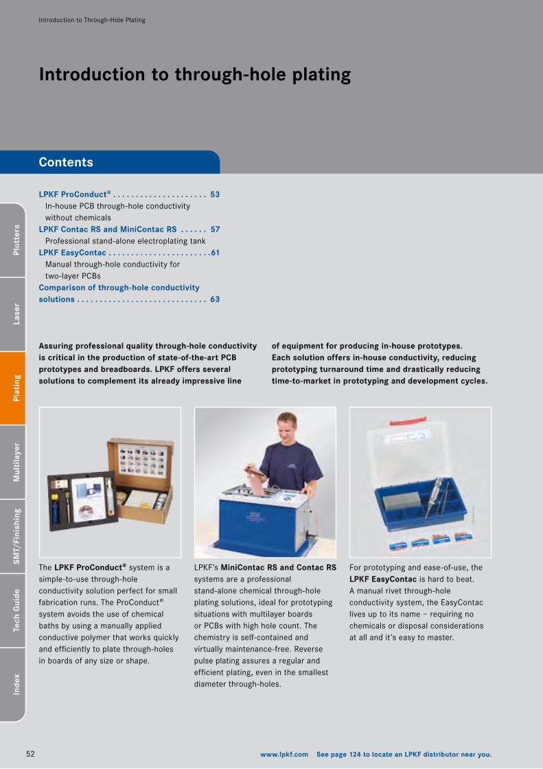
5� www.lpkf.com See page 124 to locate an LPKF distributor near you.
Plot
ters
Lase
rPl
atin
gSM
T/Fi
nish
ing
Tech
Gui
deIn
dex
Mul
tila
yer
Introduction to through-hole plating
Assuring professional quality through-hole conductivity is critical in the production of state-of-the-art PCB prototypes and breadboards. LPKF offers several solutions to complement its already impressive line
Introduction to Through-Hole Plating
LPKF’s MiniContac RS and Contac RS systems are a professional stand-alone chemical through-hole plating solutions, ideal for prototyping situations with multilayer boards or PCBs with high hole count. The chemistry is self-contained and virtually maintenance-free. Reverse pulse plating assures a regular and efficient plating, even in the smallest diameter through-holes.
The LPKF ProConduct® system is a simple-to-use through-hole conductivity solution perfect for small fabrication runs. The ProConduct® system avoids the use of chemical baths by using a manually applied conductive polymer that works quickly and efficiently to plate through-holes in boards of any size or shape.
For prototyping and ease-of-use, the LPKF EasyContac is hard to beat. A manual rivet through-hole conductivity system, the EasyContac lives up to its name – requiring no chemicals or disposal considerations at all and it’s easy to master.
LPKF ProConduct® . . . . . . . . . . . . . . . . . . . . . 53 In-house PCB through-hole conductivity without chemicalsLPKF Contac RS and MiniContac RS . . . . . . 57 Professional stand-alone electroplating tankLPKF EasyContac . . . . . . . . . . . . . . . . . . . . . . .61 Manual through-hole conductivity for two-layer PCBsComparison of through-hole conductivity solutions . . . . . . . . . . . . . . . . . . . . . . . . . . . . . 63
Contents
of equipment for producing in-house prototypes. Each solution offers in-house conductivity, reducing prototyping turnaround time and drastically reducing time-to-market in prototyping and development cycles.
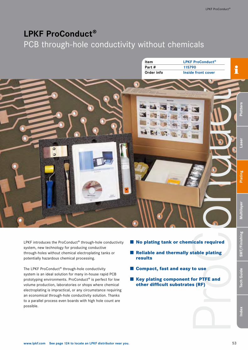
ProC
ondu
ct
53www.lpkf.com See page 124 to locate an LPKF distributor near you.
Plot
ters
Lase
rPl
atin
gSM
T/Fi
nish
ing
Tech
Gui
deIn
dex
Mul
tila
yer
Item LPKF ProConduct®Part # 115790Order info Inside front cover
LPKF ProConduct®
LPKF ProConduct® PCB through-hole conductivity without chemicals
LPKF introduces the ProConduct® through-hole conductivity system, new technology for producing conductive through-holes without chemical electroplating tanks or potentially hazardous chemical processing.
The LPKF ProConduct® through-hole conductivity system is an ideal solution for many in-house rapid PCB prototyping environments. ProConduct® is perfect for low volume production, laboratories or shops where chemical electroplating is impractical, or any circumstance requiring an economical through-hole conductivity solution. Thanks to a parallel process even boards with high hole count are possible.
No plating tank or chemicals required
Reliable and thermally stable plating results
Compact, fast and easy to use
Key plating component for PTFE and other difficult substrates (RF)
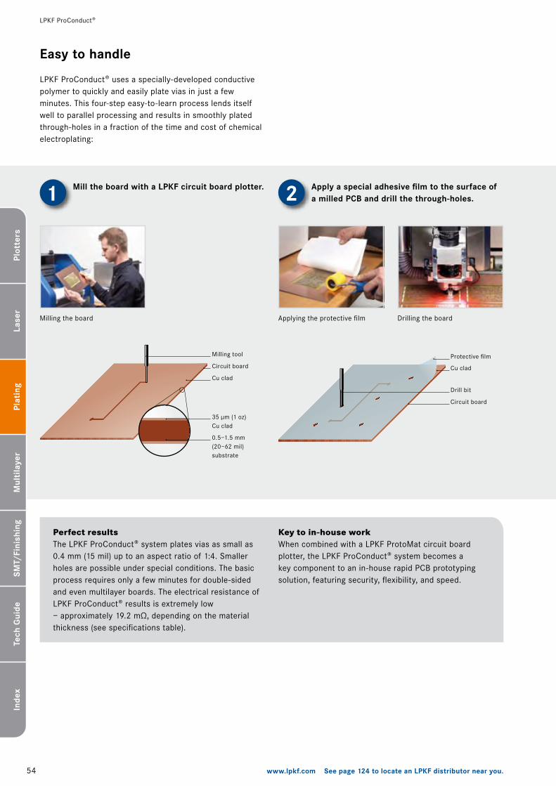
54 www.lpkf.com See page 124 to locate an LPKF distributor near you.
Plot
ters
Lase
rPl
atin
gSM
T/Fi
nish
ing
Tech
Gui
deIn
dex
Mul
tila
yer
Easy to handle
LPKF ProConduct®
Mill the board with a LPKF circuit board plotter.1
LPKF ProConduct® uses a specially-developed conductive polymer to quickly and easily plate vias in just a few minutes. This four-step easy-to-learn process lends itself well to parallel processing and results in smoothly plated through-holes in a fraction of the time and cost of chemical electroplating:
Milling the board Applying the protective film
35 µm (� oz) Cu clad
Circuit board
Milling tool
0.5–�.5 mm(�0–6� mil)substrate
Cu clad
Protective film
Drill bit
Circuit board
Cu clad
Drilling the board
The LPKF ProConduct® system plates vias as small as 0.4 mm (�5 mil) up to an aspect ratio of �:4. Smaller holes are possible under special conditions. The basic process requires only a few minutes for double-sided and even multilayer boards. The electrical resistance of LPKF ProConduct® results is extremely low – approximately �9.� mΩ, depending on the material thickness (see specifications table).
Perfect resultsWhen combined with a LPKF ProtoMat circuit board plotter, the LPKF ProConduct® system becomes a key component to an in-house rapid PCB prototyping solution, featuring security, flexibility, and speed.
Key to in-house work
Apply a special adhesive film to the surface of a milled PCB and drill the through-holes.2
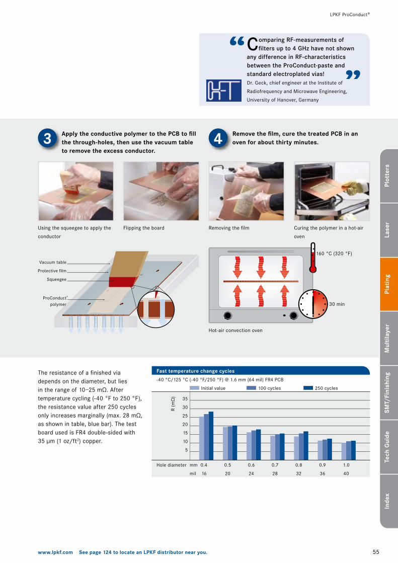
55www.lpkf.com See page 124 to locate an LPKF distributor near you.
Plot
ters
Lase
rPl
atin
gSM
T/Fi
nish
ing
Tech
Gui
deIn
dex
Mul
tila
yer
LPKF ProConduct®
Apply the conductive polymer to the PCB to fill the through-holes, then use the vacuum table to remove the excess conductor.
Remove the film, cure the treated PCB in an oven for about thirty minutes.
Removing the filmUsing the squeegee to apply the
conductor
Flipping the board Curing the polymer in a hot-air
oven
Protective film
ProConduct® polymer
Vacuum table
Hot-air convection oven
30 min
�60 °C (3�0 °F)
Squeegee
3 4
Initial value �00 cycles �50 cycles
Fast temperature change cycles
35
30
�5
�0
�5
�0
5
0.4
�6
0.5
�0
0.6
�4
0.7
�8
0.8
3�
0.9
36
�.0
40
-40 °C/��5 °C (-40 °F/�50 °F) @ �.6 mm (64 mil) FR4 PCB
R (m
Ω)
Hole diameter mm
mil
The resistance of a finished via depends on the diameter, but lies in the range of �0–�5 mΩ. After temperature cycling (-40 °F to �50 °F), the resistance value after �50 cycles only increases marginally (max. �8 mΩ, as shown in table, blue bar). The test board used is FR4 double-sided with 35 µm (� oz/ft�) copper.
Comparing RF-measurements of filters up to 4 GHz have not shown
any difference in RF-characteristics between the ProConduct-paste and standard electroplated vias! Dr. Geck, chief engineer at the Institute of
Radiofrequency and Microwave Engineering,
University of Hanover, Germany
“”
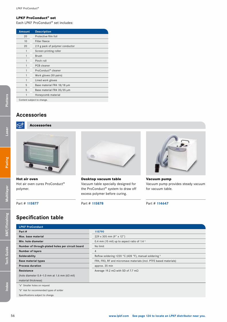
56 www.lpkf.com See page 124 to locate an LPKF distributor near you.
Plot
ters
Lase
rPl
atin
gSM
T/Fi
nish
ing
Tech
Gui
deIn
dex
Mul
tila
yer
Part #
Max. base material
Min. hole diameter
Number of through-plated holes per circuit board
Number of layers
Solderability
Base material types
Process duration
Resistance
(hole diameter 0.4–�.0 mm at �.6 mm (63 mil)
material thickness)
115790
��9 x 305 mm (9’’ x ��’’)
0.4 mm (�5 mil) up to aspect ratio of �:4 a
No limit
4
Reflow soldering <��0 °C (4�8 °F), manual soldering b
FR4, FR3, RF and micromave materials (incl. PTFE based materials)
approx. 35 min
Average �9.� mΩ with SD of 7.7 mΩ
LPKF ProConduct
Specification table
“a” Smaller holes on request
“b” Ask for recommended types of solder
Specifications subject to change.
Accessories
Accessories
LPKF ProConduct®
LPKF ProConduct® setEach LPKF ProConduct® set includes:
�0
�0
�0
�
�
�
�
�
�
�
5
5
�
Description
Protective film foil
Filter fleece
�.9 g pack of polymer conductor
Screen printing roller
Brush
Pinch roll
PCB cleaner
ProConduct® cleaner
Work gloves (50 pairs)
Lined work gloves
Base material FR4 �8/�8 µm
Base material FR4 35/35 µm
Honeycomb material
Amount
Content subject to change.
Hot air ovenHot air oven cures ProConduct® polymer.
Part # 115877
Desktop vacuum tableVacuum table specially designed for the ProConduct® system to draw off excess polymer before curing.
Part # 115878
Vacuum pumpVacuum pump provides steady vacuum for vacuum table.
Part # 114647
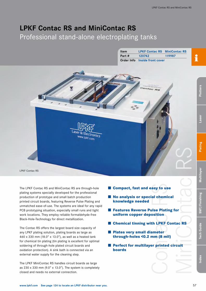
Con
tac
RSM
iniC
onta
c RS
57www.lpkf.com See page 124 to locate an LPKF distributor near you.
Plot
ters
Lase
rPl
atin
gSM
T/Fi
nish
ing
Tech
Gui
deIn
dex
Mul
tila
yer
LPKF Contac RS and MiniContac RS
Item LPKF Contac RS MiniContac RSPart # 120742 119987Order Info Inside front cover
LPKF Contac RS and MiniContac RS Professional stand-alone electroplating tanks
The LPKF Contac RS and MiniContac RS are through-hole plating systems specially developed for the professional production of prototype and small batch production printed circuit boards, featuring Reverse Pulse Plating and unmatched ease-of-use. The systems are ideal for any rapid PCB prototyping situation, especially small runs and tight work locations. They employ reliable formaldehyde-free Black-Hole-Technology for direct metallization.
The Contac RS offers the largest board size capacity of any LPKF plating solution, plating boards as large as 460 x 330 mm (�8.0” x �3.0”), as well as a heated tank for chemical tin plating (tin plating is excellent for optimal soldering of through-hole plated circuit boards and oxidation protection). A sink bath is connected via an external water supply for the cleaning step.
The LPKF MiniContac RS handles circuit boards as large as �30 x 330 mm (9.0” x �3.0”). The system is completely closed and needs no external connection.
Compact, fast and easy to use
No analysis or special chemical knowledge needed
Features Reverse Pulse Plating for uniform copper deposition
Chemical tinning with LPKF Contac RS
Plates very small diameter through-holes <0.2 mm (8 mil)
Perfect for multilayer printed circuit boards
LPKF Contac RS
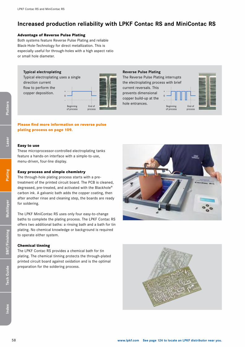
58 www.lpkf.com See page 124 to locate an LPKF distributor near you.
Plot
ters
Lase
rPl
atin
gSM
T/Fi
nish
ing
Tech
Gui
deIn
dex
Mul
tila
yer
LPKF Contac RS and MiniContac RS
Increased production reliability with LPKF Contac RS and MiniContac RS
Advantage of Reverse Pulse PlatingBoth systems feature Reverse Pulse Plating and reliable Black-Hole-Technology for direct metallization. This is especially useful for through-holes with a high aspect ratio or small hole diameter.
Easy to useThese microprocessor-controlled electroplating tanks feature a hands-on interface with a simple-to-use, menu-driven, four-line display.
Easy process and simple chemistryThe through-hole plating process starts with a pre-treatment of the printed circuit board. The PCB is cleaned, degreased, pre-treated, and activated with the Blackhole® carbon ink. A galvanic bath adds the copper coating, then after another rinse and cleaning step, the boards are ready for soldering.
The LPKF MiniContac RS uses only four easy-to-change baths to complete the plating process. The LPKF Contac RS offers two additional baths: a rinsing bath and a bath for tin plating. No chemical knowledge or background is required to operate either system.
Please find more information on reverse pulse plating process on page 109.
Typical electroplating uses a single direction current flow to perform the copper deposition.
The Reverse Pulse Plating interrupts the electroplating process with brief current reversals. This prevents dimensional copper build-up at the hole entrances.
Typical electroplating Reverse Pulse Plating
Chemical tinningThe LPKF Contac RS provides a chemical bath for tin plating. The chemical tinning protects the through-plated printed circuit board against oxidation and is the optimal preparation for the soldering process.
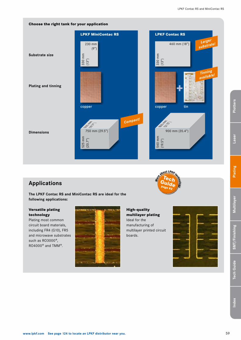
59www.lpkf.com See page 124 to locate an LPKF distributor near you.
Plot
ters
Lase
rPl
atin
gSM
T/Fi
nish
ing
Tech
Gui
deIn
dex
Mul
tila
yer
LPKF Contac RS and MiniContac RS
Versatile plating technologyPlating most common circuit board materials, including FR4 (G�0), FR5 and microwave substrates such as RO3000®, RO4000® and TMM®.
The LPKF Contac RS and MiniContac RS are ideal for the following applications:
Applications
High-quality multilayer platingIdeal for the manufacturing of multilayer printed circuit boards.
LPKF Contac RS LPKF MiniContac RS
Choose the right tank for your application
Substrate size
460 mm (�8”)
330
mm
(�
3”)
�30 mm (9”)
Dimensions 900 mm (35.4”)
540
mm
(�
9.5”
)
800 mm
(3�.5”)
750 mm (�9.5”)
5�5
mm
(�
0.7”
)
500 mm
(�9.7”)
Plating and tinning33
0 m
m
(�3”
)
copper tincopper
+Tinning
available!
Larger
substrate!
Compact!
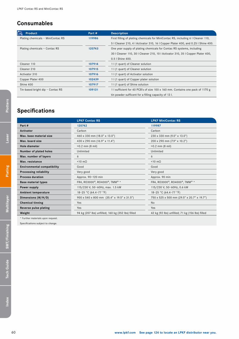
60 www.lpkf.com See page 124 to locate an LPKF distributor near you.
Plot
ters
Lase
rPl
atin
gSM
T/Fi
nish
ing
Tech
Gui
deIn
dex
Mul
tila
yer
Part #
Activator
Max. base material size
Max. board size
Hole diameter
Number of plated holes
Max. number of layers
Max. resistance
Environmental compatibility
Processing reliability
Process duration
Base material types
Power supply
Ambient temperature
Dimensions (W/H/D)
Chemical tinning
Reverse pulse plating
Weight
120742
Carbon
460 x 330 mm (�8.0” x �3.0”)
430 x �90 mm (�6.9” x ��.4”)
>0.� mm (8 mil)
Unlimited
6
<�0 mΩ
Good
Very good
Approx. 90–��0 min
FR4, RO3000®, RO4000®, TMM® *
��5/�30 V, 50–60Hz, max. �.5 kW
�8–�5 °C (64.4–77 °F)
900 x 540 x 800 mm (35.4” x �9.5” x 3�.5”)
Yes
Yes
94 kg (�07 lbs) unfilled; �60 kg (35� lbs) filled
LPKF Contac RS
119987
Carbon
�30 x 330 mm (9.0” x �3.0”)
�00 x �90 mm (7.9“ x �0.�”)
>0.� mm (8 mil)
Unlimited
6
<�0 mΩ
Good
Very good
Approx. 90 min
FR4, RO3000®, RO4000®, TMM® *
��5/�30 V, 50–60Hz, 0.6 kW
�8–�5 °C (64.4–77 °F)
750 x 5�5 x 500 mm (�9.5” x �0.7” x �9.7”)
No
Yes
4� kg (9� lbs) unfilled; 7� kg (�56 lbs) filled
LPKF MiniContac RS
* Further materials upon request.
Specifications
LPKF Contac RS and MiniContac RS
Consumables
Part #Product
Plating chemicals – MiniContac RS
Plating chemicals – Contac RS
Cleaner ��0
Cleaner ��0
Activator 3�0
Copper Plater 400
Shine 400
Tin-based bright dip – Contac RS
First filling of plating chemicals for MiniContac RS, including 6 l Cleaner ��0,
5 l Cleaner ��0, 4 l Activator 3�0, �6 l Copper Plater 400, and 0.�5 l Shine 400.
One year supply of plating chemicals for Contac RS systems, including
30 l Cleaner ��0, 30 l Cleaner ��0, �0 l Activator 3�0, 35 l Copper Plater 400,
0.5 l Shine 400.
� l (� quart) of Cleaner solution
� l (� quart) of Cleaner solution
� l (� quart) of Activator solution
� l (� quart) of Copper plater solution
� l (� quart) of Shine solution
� l sufficient for 40 PCB’s of size �00 x �60 mm. Contains one pack of ��70 g
tin powder sufficent for a filling capacity of �3 l.
Description
Specifications subject to change.
119986
120743
107914
107915
107916
102439
107917
109131
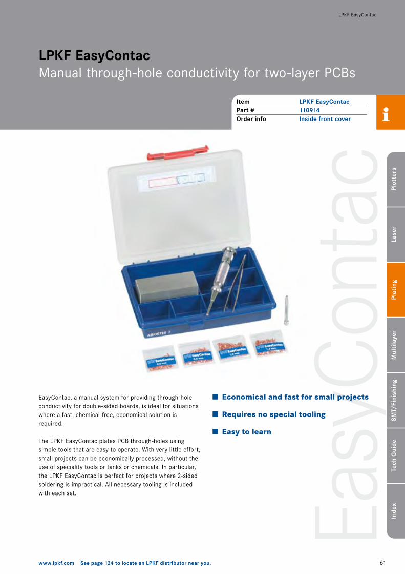
Easy
Con
tac
6�www.lpkf.com See page 124 to locate an LPKF distributor near you.
Plot
ters
Lase
rPl
atin
gSM
T/Fi
nish
ing
Tech
Gui
deIn
dex
Mul
tila
yer
LPKF EasyContac
Item LPKF EasyContacPart # 110914Order info Inside front cover
LPKF EasyContac Manual through-hole conductivity for two-layer PCBs
EasyContac, a manual system for providing through-hole conductivity for double-sided boards, is ideal for situations where a fast, chemical-free, economical solution is required.
The LPKF EasyContac plates PCB through-holes using simple tools that are easy to operate. With very little effort, small projects can be economically processed, without the use of speciality tools or tanks or chemicals. In particular, the LPKF EasyContac is perfect for projects where �-sided soldering is impractical. All necessary tooling is included with each set.
Economical and fast for small projects
Requires no special tooling
Easy to learn
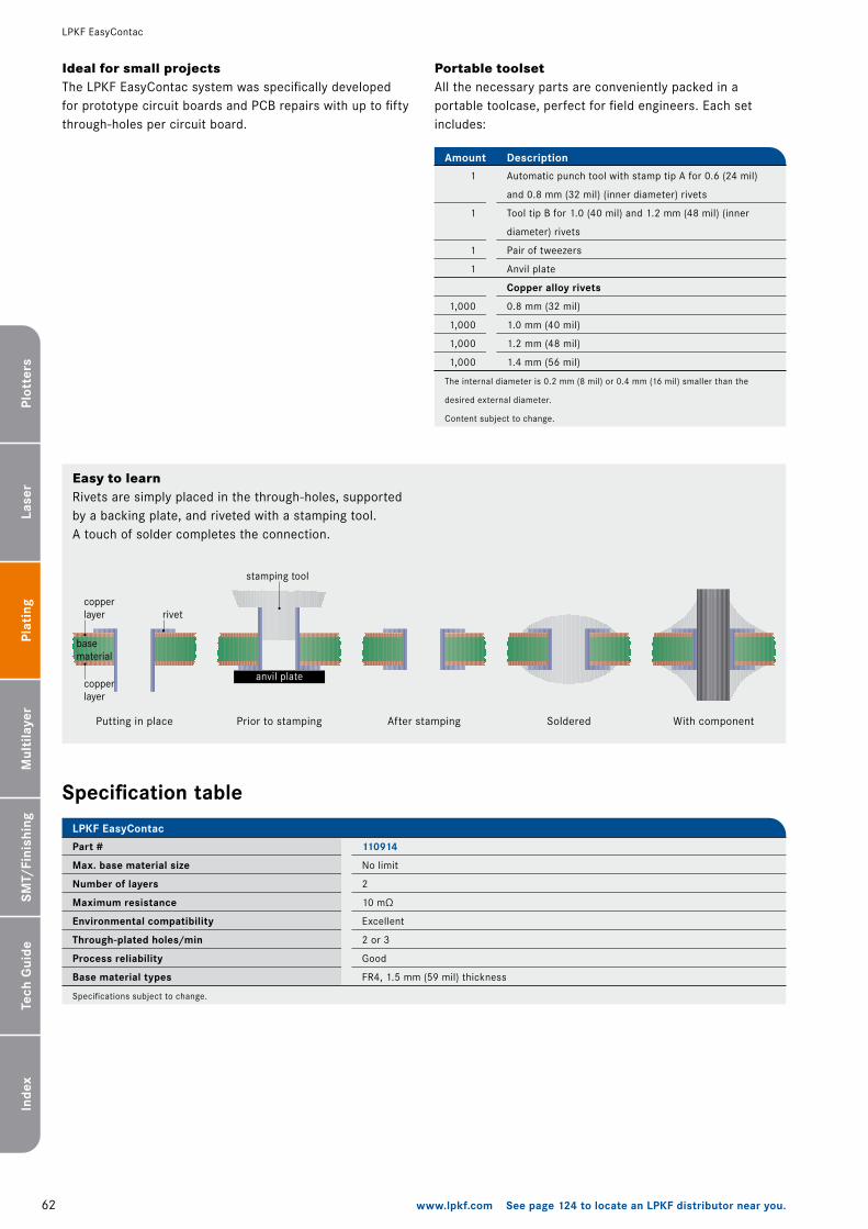
copperlayer rivet
copperlayer
basematerial
anvil plate
stamping tool
6� www.lpkf.com See page 124 to locate an LPKF distributor near you.
Plot
ters
Lase
rPl
atin
gSM
T/Fi
nish
ing
Tech
Gui
deIn
dex
Mul
tila
yer
LPKF EasyContac
Ideal for small projectsThe LPKF EasyContac system was specifically developed for prototype circuit boards and PCB repairs with up to fifty through-holes per circuit board.
Portable toolsetAll the necessary parts are conveniently packed in a portable toolcase, perfect for field engineers. Each set includes:
Easy to learnRivets are simply placed in the through-holes, supported by a backing plate, and riveted with a stamping tool. A touch of solder completes the connection.
�
�
�
�
�,000
�,000
�,000
�,000
Description
Automatic punch tool with stamp tip A for 0.6 (�4 mil)
and 0.8 mm (3� mil) (inner diameter) rivets
Tool tip B for �.0 (40 mil) and �.� mm (48 mil) (inner
diameter) rivets
Pair of tweezers
Anvil plate
Copper alloy rivets
0.8 mm (3� mil)
�.0 mm (40 mil)
�.� mm (48 mil)
�.4 mm (56 mil)
Amount
The internal diameter is 0.� mm (8 mil) or 0.4 mm (�6 mil) smaller than the
desired external diameter.
Part #
Max. base material size
Number of layers
Maximum resistance
Environmental compatibility
Through-plated holes/min
Process reliability
Base material types
110914
No limit
�
�0 mΩ
Excellent
� or 3
Good
FR4, �.5 mm (59 mil) thickness
LPKF EasyContac
Specification table
Specifications subject to change.
Putting in place Prior to stamping After stamping Soldered With component
Content subject to change.
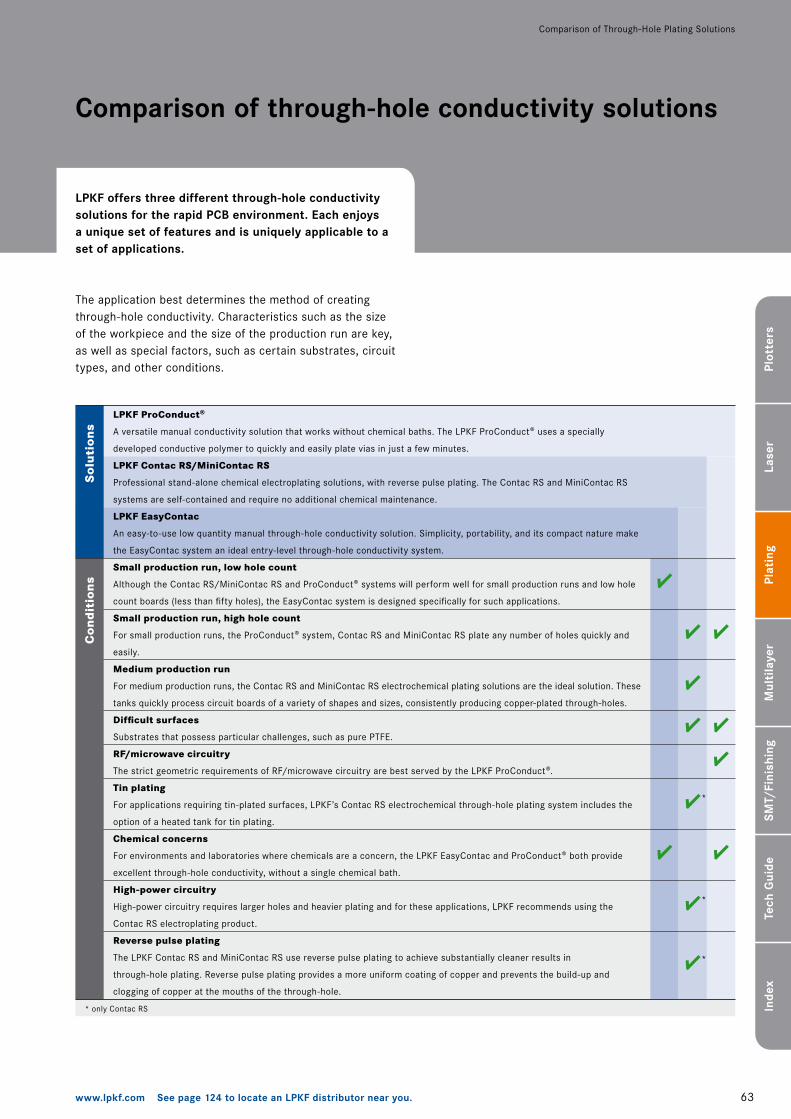
63www.lpkf.com See page 124 to locate an LPKF distributor near you.
Plot
ters
Lase
rPl
atin
gSM
T/Fi
nish
ing
Tech
Gui
deIn
dex
Mul
tila
yer
Comparison of Through-Hole Plating Solutions
Comparison of through-hole conductivity solutions
LPKF offers three different through-hole conductivity solutions for the rapid PCB environment. Each enjoys a unique set of features and is uniquely applicable to a set of applications.
LPKF ProConduct®
A versatile manual conductivity solution that works without chemical baths. The LPKF ProConduct® uses a specially
developed conductive polymer to quickly and easily plate vias in just a few minutes.
LPKF Contac RS/MiniContac RS
Professional stand-alone chemical electroplating solutions, with reverse pulse plating. The Contac RS and MiniContac RS
systems are self-contained and require no additional chemical maintenance.
LPKF EasyContac
An easy-to-use low quantity manual through-hole conductivity solution. Simplicity, portability, and its compact nature make
the EasyContac system an ideal entry-level through-hole conductivity system.
Small production run, low hole count
Although the Contac RS/MiniContac RS and ProConduct® systems will perform well for small production runs and low hole
count boards (less than fifty holes), the EasyContac system is designed specifically for such applications.
Small production run, high hole count
For small production runs, the ProConduct® system, Contac RS and MiniContac RS plate any number of holes quickly and
easily.
Medium production run
For medium production runs, the Contac RS and MiniContac RS electrochemical plating solutions are the ideal solution. These
tanks quickly process circuit boards of a variety of shapes and sizes, consistently producing copper-plated through-holes.
Difficult surfaces
Substrates that possess particular challenges, such as pure PTFE.
RF/microwave circuitry
The strict geometric requirements of RF/microwave circuitry are best served by the LPKF ProConduct®.
Tin plating
For applications requiring tin-plated surfaces, LPKF’s Contac RS electrochemical through-hole plating system includes the
option of a heated tank for tin plating.
Chemical concerns
For environments and laboratories where chemicals are a concern, the LPKF EasyContac and ProConduct® both provide
excellent through-hole conductivity, without a single chemical bath.
High-power circuitry
High-power circuitry requires larger holes and heavier plating and for these applications, LPKF recommends using the
Contac RS electroplating product.
Reverse pulse plating
The LPKF Contac RS and MiniContac RS use reverse pulse plating to achieve substantially cleaner results in
through-hole plating. Reverse pulse plating provides a more uniform coating of copper and prevents the build-up and
clogging of copper at the mouths of the through-hole.
* only Contac RS
*
*
*
The application best determines the method of creating through-hole conductivity. Characteristics such as the size of the workpiece and the size of the production run are key, as well as special factors, such as certain substrates, circuit types, and other conditions.
So
luti
ons
Con
dit
ion
s
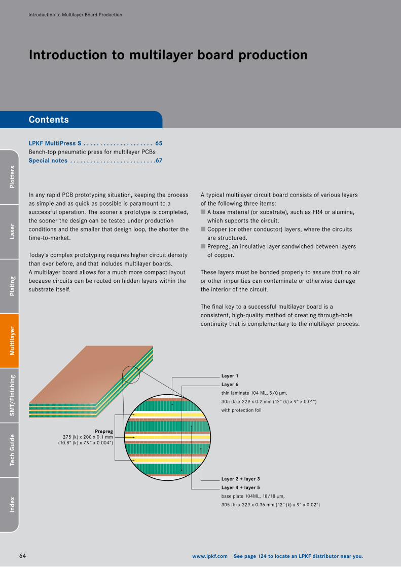
64 www.lpkf.com See page 124 to locate an LPKF distributor near you.
Plot
ters
Lase
rPl
atin
gSM
T/Fi
nish
ing
Tech
Gui
deIn
dex
Mul
tila
yer
Introduction to multilayer board production
In any rapid PCB prototyping situation, keeping the process as simple and as quick as possible is paramount to a successful operation. The sooner a prototype is completed, the sooner the design can be tested under production conditions and the smaller that design loop, the shorter the time-to-market.
Today’s complex prototyping requires higher circuit density than ever before, and that includes multilayer boards. A multilayer board allows for a much more compact layout because circuits can be routed on hidden layers within the substrate itself.
Introduction to Multilayer Board Production
LPKF MultiPress S . . . . . . . . . . . . . . . . . . . . . 65Bench-top pneumatic press for multilayer PCBsSpecial notes . . . . . . . . . . . . . . . . . . . . . . . . . .67
Contents
A typical multilayer circuit board consists of various layers of the following three items: A base material (or substrate), such as FR4 or alumina, which supports the circuit. Copper (or other conductor) layers, where the circuits are structured. Prepreg, an insulative layer sandwiched between layers of copper.
These layers must be bonded properly to assure that no air or other impurities can contaminate or otherwise damage the interior of the circuit.
The final key to a successful multilayer board is a consistent, high-quality method of creating through-hole continuity that is complementary to the multilayer process.
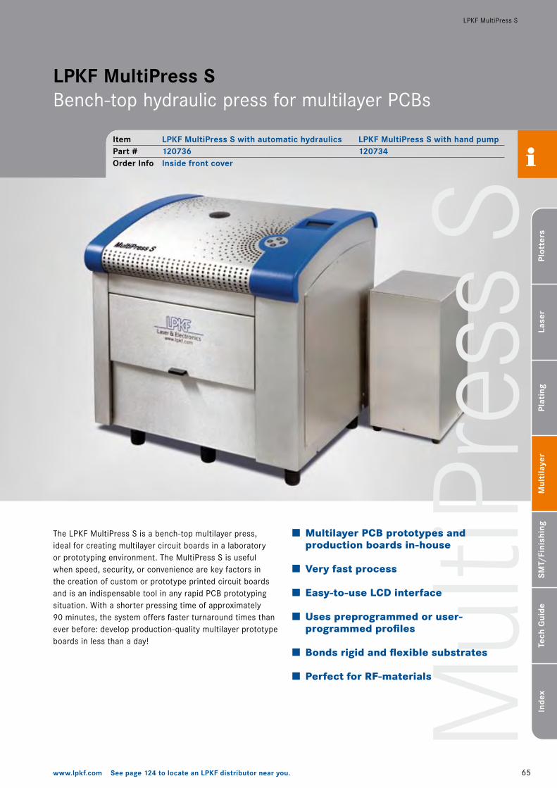
Mul
tiPre
ss S
65www.lpkf.com See page 124 to locate an LPKF distributor near you.
Plot
ters
Lase
rPl
atin
gSM
T/Fi
nish
ing
Tech
Gui
deIn
dex
Mul
tila
yer
LPKF MultiPress S
LPKF MultiPress S Bench-top hydraulic press for multilayer PCBs
The LPKF MultiPress S is a bench-top multilayer press, ideal for creating multilayer circuit boards in a laboratory or prototyping environment. The MultiPress S is useful when speed, security, or convenience are key factors in the creation of custom or prototype printed circuit boards and is an indispensable tool in any rapid PCB prototyping situation. With a shorter pressing time of approximately 90 minutes, the system offers faster turnaround times than ever before: develop production-quality multilayer prototype boards in less than a day!
Multilayer PCB prototypes and production boards in-house
Very fast process
Easy-to-use LCD interface
Uses preprogrammed or user- programmed profiles
Bonds rigid and flexible substrates
Perfect for RF-materials
Item LPKF MultiPress S with automatic hydraulics LPKF MultiPress S with hand pumpPart # 120736 120734Order Info Inside front cover
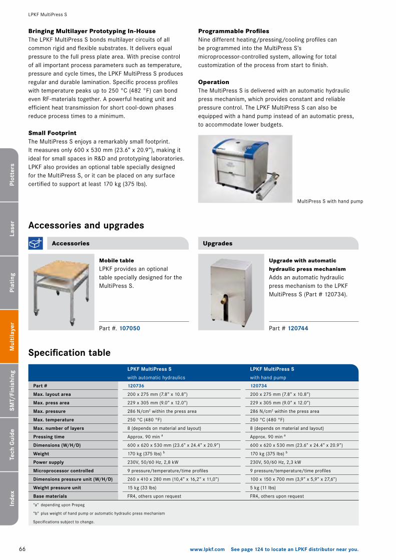
66 www.lpkf.com See page 124 to locate an LPKF distributor near you.
Plot
ters
Lase
rPl
atin
gSM
T/Fi
nish
ing
Tech
Gui
deIn
dex
Mul
tila
yer
Specification table
Accessories
Accessories and upgrades
LPKF MultiPress S
Mobile tableLPKF provides an optional table specially designed for the MultiPress S.
Part #. 107050
Small FootprintThe MultiPress S enjoys a remarkably small footprint. It measures only 600 x 530 mm (�3.6” x �0.9”), making it ideal for small spaces in R&D and prototyping laboratories. LPKF also provides an optional table specially designed for the MultiPress S, or it can be placed on any surface certified to support at least �70 kg (375 lbs).
Programmable ProfilesNine different heating/pressing/cooling profiles can be programmed into the MultiPress S’s microprocessor-controlled system, allowing for total customization of the process from start to finish.
Bringing Multilayer Prototyping In-HouseThe LPKF MultiPress S bonds multilayer circuits of all common rigid and flexible substrates. It delivers equal pressure to the full press plate area. With precise control of all important process parameters such as temperature, pressure and cycle times, the LPKF MultiPress S produces regular and durable lamination. Specific process profiles with temperature peaks up to �50 °C (48� °F) can bond even RF-materials together. A powerful heating unit and efficient heat transmission for short cool-down phases reduce process times to a minimum.
OperationThe MultiPress S is delivered with an automatic hydraulic press mechanism, which provides constant and reliable pressure control. The LPKF MultiPress S can also be equipped with a hand pump instead of an automatic press, to accommodate lower budgets.
Upgrades
Upgrade with automatic hydraulic press mechanismAdds an automatic hydraulic press mechanism to the LPKF MultiPress S (Part # ��0734).
Part # 120744
MultiPress S with hand pump
LPKF MultiPress S
with automatic hydraulics
LPKF MultiPress S
with hand pump
Part #
Max. layout area
Max. press area
Max. pressure
Max. temperature
Max. number of layers
Pressing time
Dimensions (W/H/D)
Weight
Power supply
Microprocessor controlled
Dimensions pressure unit (W/H/D)
Weight pressure unit
Base materials
120736
�00 x �75 mm (7.8” x �0.8”)
��9 x 305 mm (9.0” x ��.0”)
�86 N/cm� within the press area
�50 °C (480 °F)
8 (depends on material and layout)
Approx. 90 min a
600 x 6�0 x 530 mm (�3.6” x �4.4” x �0.9”)
�70 kg (375 lbs) b
�30V, 50/60 Hz, �,8 kW
9 pressure/temperature/time profiles
�60 x 4�0 x �80 mm (�0,4” x �6,�” x ��,0”)
�5 kg (33 lbs)
FR4, others upon request
“a” depending upon Prepeg
“b” plus weight of hand pump or automatic hydraulic press mechanism
Specifications subject to change.
120734
�00 x �75 mm (7.8” x �0.8”)
��9 x 305 mm (9.0” x ��.0”)
�86 N/cm� within the press area
�50 °C (480 °F)
8 (depends on material and layout)
Approx. 90 min a
600 x 6�0 x 530 mm (�3.6” x �4.4” x �0.9”)
�70 kg (375 lbs) b
�30V, 50/60 Hz, �,3 kW
9 pressure/temperature/time profiles
�00 x �50 x 700 mm (3,9” x 5,9” x �7,6”)
5 kg (�� lbs)
FR4, others upon request
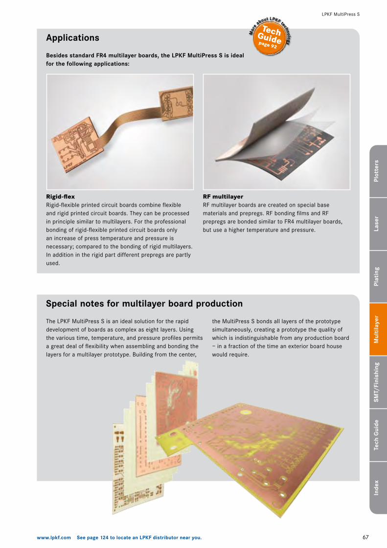
67www.lpkf.com See page 124 to locate an LPKF distributor near you.
Plot
ters
Lase
rPl
atin
gSM
T/Fi
nish
ing
Tech
Gui
deIn
dex
Mul
tila
yer
LPKF MultiPress S
Special notes for multilayer board production
The LPKF MultiPress S is an ideal solution for the rapid development of boards as complex as eight layers. Using the various time, temperature, and pressure profiles permits a great deal of flexibility when assembling and bonding the layers for a multilayer prototype. Building from the center,
the MultiPress S bonds all layers of the prototype simultaneously, creating a prototype the quality of which is indistinguishable from any production board – in a fraction of the time an exterior board house would require.
Rigid-flexRigid-flexible printed circuit boards combine flexible and rigid printed circuit boards. They can be processed in principle similar to multilayers. For the professional bonding of rigid-flexible printed circuit boards only an increase of press temperature and pressure is necessary; compared to the bonding of rigid multilayers. In addition in the rigid part different prepregs are partly used.
Besides standard FR4 multilayer boards, the LPKF MultiPress S is ideal for the following applications:
Applications
RF multilayerRF multilayer boards are created on special base materials and prepregs. RF bonding films and RF prepregs are bonded similar to FR4 multilayer boards, but use a higher temperature and pressure.
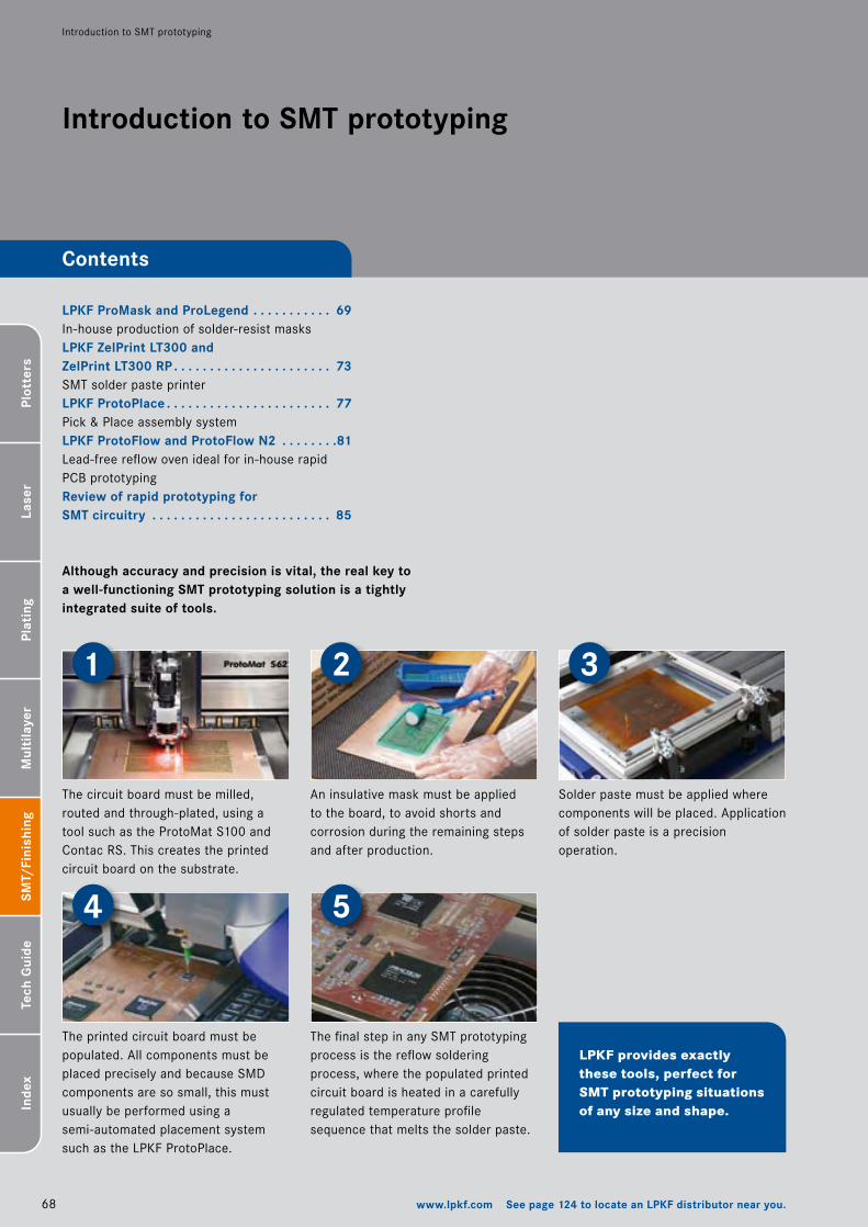
68 www.lpkf.com See page 124 to locate an LPKF distributor near you.
Plot
ters
Lase
rPl
atin
gSM
T/Fi
nish
ing
Tech
Gui
deIn
dex
Mul
tila
yer
Introduction to SMT prototyping
Although accuracy and precision is vital, the real key to a well-functioning SMT prototyping solution is a tightly integrated suite of tools.
Introduction to SMT prototyping
LPKF ProMask and ProLegend . . . . . . . . . . . 69In-house production of solder-resist masksLPKF ZelPrint LT300 and ZelPrint LT300 RP . . . . . . . . . . . . . . . . . . . . . . 73SMT solder paste printerLPKF ProtoPlace . . . . . . . . . . . . . . . . . . . . . . . 77Pick & Place assembly systemLPKF ProtoFlow and ProtoFlow N2 . . . . . . . .81Lead-free reflow oven ideal for in-house rapid PCB prototypingReview of rapid prototyping for SMT circuitry . . . . . . . . . . . . . . . . . . . . . . . . . 85
Contents
The circuit board must be milled, routed and through-plated, using a tool such as the ProtoMat S�00 and Contac RS. This creates the printed circuit board on the substrate.
An insulative mask must be applied to the board, to avoid shorts and corrosion during the remaining steps and after production.
Solder paste must be applied where components will be placed. Application of solder paste is a precision operation.
The printed circuit board must be populated. All components must be placed precisely and because SMD components are so small, this must usually be performed using a semi-automated placement system such as the LPKF ProtoPlace.
The final step in any SMT prototyping process is the reflow soldering process, where the populated printed circuit board is heated in a carefully regulated temperature profile sequence that melts the solder paste.
LPKF provides exactly these tools, perfect for SMT prototyping situations of any size and shape.
1 2 3
4 5
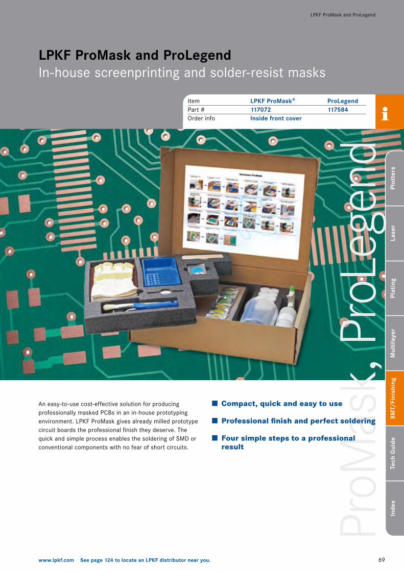
ProM
ask,
Pro
Lege
nd
69www.lpkf.com See page 124 to locate an LPKF distributor near you.
Plot
ters
Lase
rPl
atin
gSM
T/Fi
nish
ing
Tech
Gui
deIn
dex
Mul
tila
yer
LPKF ProMask and ProLegend
LPKF ProMask and ProLegend In-house screenprinting and solder-resist masks
An easy-to-use cost-effective solution for producing professionally masked PCBs in an in-house prototyping environment. LPKF ProMask gives already milled prototype circuit boards the professional finish they deserve. The quick and simple process enables the soldering of SMD or conventional components with no fear of short circuits.
Compact, quick and easy to use
Professional finish and perfect soldering
Four simple steps to a professional result
Item LPKF ProMask® ProLegendPart # 117072 117584Order info Inside front cover
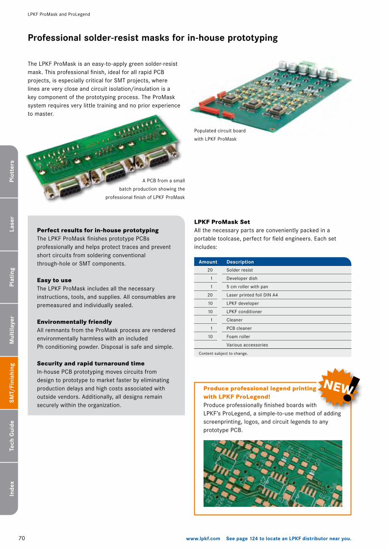
70 www.lpkf.com See page 124 to locate an LPKF distributor near you.
Plot
ters
Lase
rPl
atin
gSM
T/Fi
nish
ing
Tech
Gui
deIn
dex
Mul
tila
yer
!
The LPKF ProMask is an easy-to-apply green solder-resist mask. This professional finish, ideal for all rapid PCB projects, is especially critical for SMT projects, where lines are very close and circuit isolation/insulation is a key component of the prototyping process. The ProMask system requires very little training and no prior experience to master.
LPKF ProMask and ProLegend
Perfect results for in-house prototypingThe LPKF ProMask finishes prototype PCBs professionally and helps protect traces and prevent short circuits from soldering conventional through-hole or SMT components.
Easy to useThe LPKF ProMask includes all the necessary instructions, tools, and supplies. All consumables are premeasured and individually sealed.
Environmentally friendlyAll remnants from the ProMask process are rendered environmentally harmless with an included Ph conditioning powder. Disposal is safe and simple.
Security and rapid turnaround timeIn-house PCB prototyping moves circuits from design to prototype to market faster by eliminating production delays and high costs associated with outside vendors. Additionally, all designs remain securely within the organization.
A PCB from a small
batch production showing the
professional finish of LPKF ProMask
Populated circuit board
with LPKF ProMask
Professional solder-resist masks for in-house prototyping
Produce professional legend printing with LPKF ProLegend!Produce professionally finished boards with LPKF’s ProLegend, a simple-to-use method of adding screenprinting, logos, and circuit legends to any prototype PCB.
�0
�
�
�0
�0
�0
�
�
�0
Description
Solder resist
Developer dish
5 cm roller with pan
Laser printed foil DIN A4
LPKF developer
LPKF conditioner
Cleaner
PCB cleaner
Foam roller
Various accessories
Amount
LPKF ProMask SetAll the necessary parts are conveniently packed in a portable toolcase, perfect for field engineers. Each set includes:
Content subject to change.
!NEW
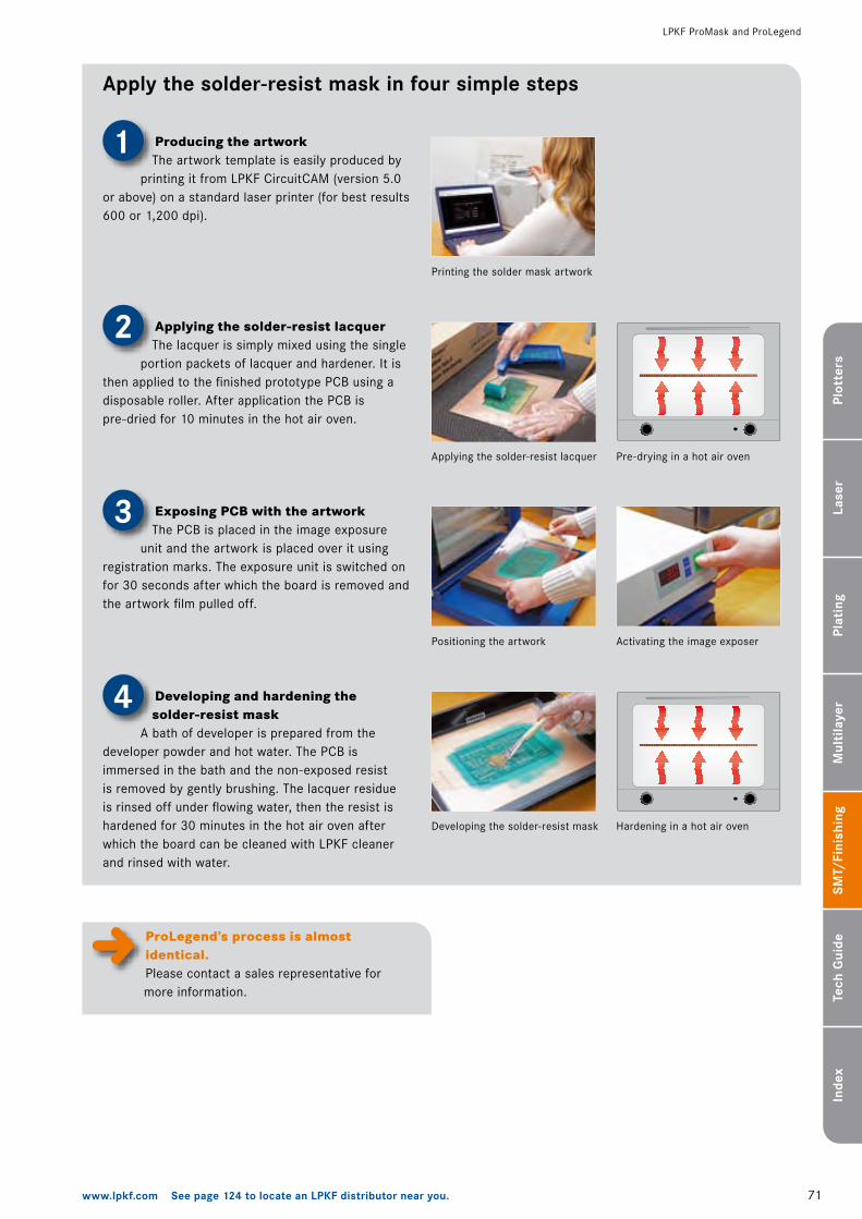
7�www.lpkf.com See page 124 to locate an LPKF distributor near you.
Plot
ters
Lase
rPl
atin
gSM
T/Fi
nish
ing
Tech
Gui
deIn
dex
Mul
tila
yer
LPKF ProMask and ProLegend
1
2
3
4
Producing the artworkThe artwork template is easily produced by
printing it from LPKF CircuitCAM (version 5.0 or above) on a standard laser printer (for best results 600 or �,�00 dpi).
Printing the solder mask artwork
Applying the solder-resist lacquer
Positioning the artwork Activating the image exposer
Developing the solder-resist mask
Apply the solder-resist mask in four simple steps
Pre-drying in a hot air oven
Hardening in a hot air oven
Applying the solder-resist lacquerThe lacquer is simply mixed using the single
portion packets of lacquer and hardener. It is then applied to the finished prototype PCB using a disposable roller. After application the PCB is pre-dried for �0 minutes in the hot air oven.
Exposing PCB with the artworkThe PCB is placed in the image exposure
unit and the artwork is placed over it using registration marks. The exposure unit is switched on for 30 seconds after which the board is removed and the artwork film pulled off.
Developing and hardening the solder-resist mask
A bath of developer is prepared from the developer powder and hot water. The PCB is immersed in the bath and the non-exposed resist is removed by gently brushing. The lacquer residue is rinsed off under flowing water, then the resist is hardened for 30 minutes in the hot air oven after which the board can be cleaned with LPKF cleaner and rinsed with water.
ProLegend’s process is almost identical.Please contact a sales representative for more information.
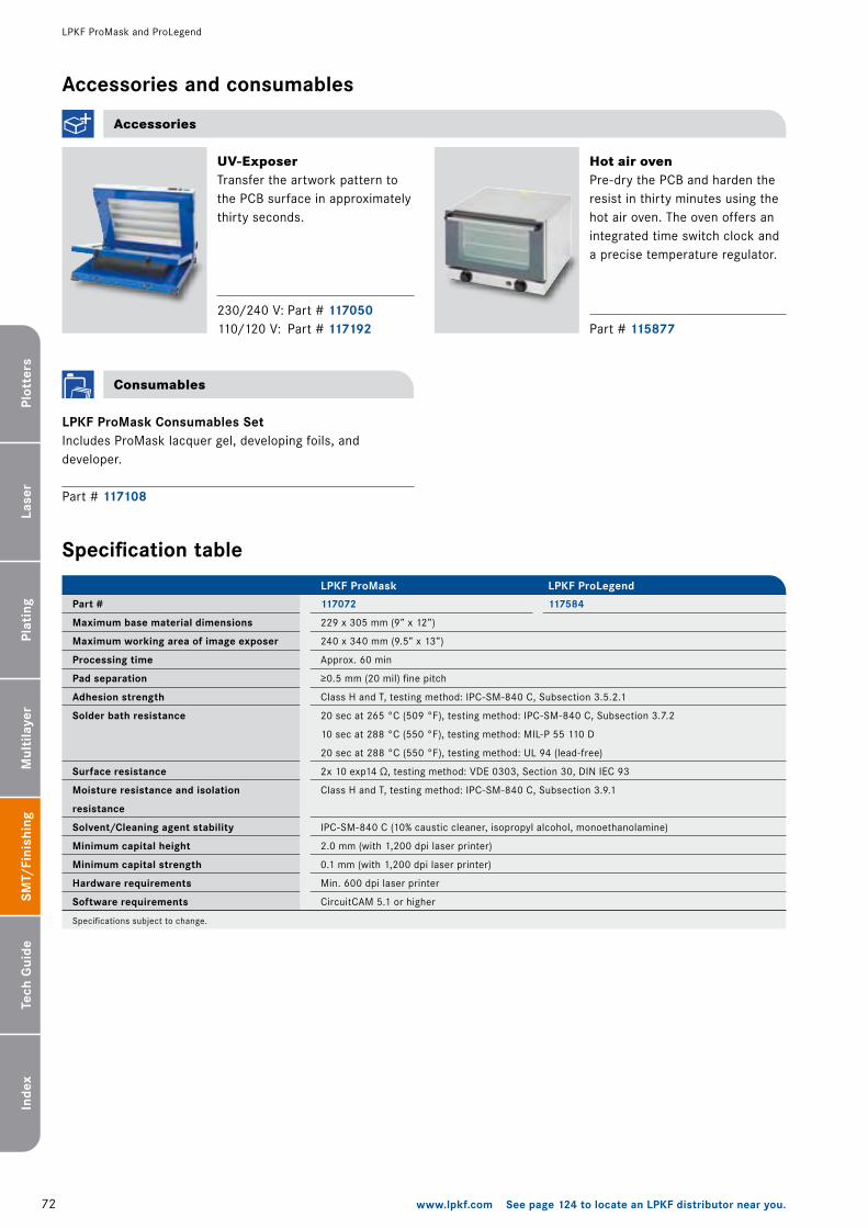
7� www.lpkf.com See page 124 to locate an LPKF distributor near you.
Plot
ters
Lase
rPl
atin
gSM
T/Fi
nish
ing
Tech
Gui
deIn
dex
Mul
tila
yer
LPKF ProMask and ProLegend
Part #
Maximum base material dimensions
Maximum working area of image exposer
Processing time
Pad separation
Adhesion strength
Solder bath resistance
Surface resistance
Moisture resistance and isolation
resistance
Solvent/Cleaning agent stability
Minimum capital height
Minimum capital strength
Hardware requirements
Software requirements
117072
��9 x 305 mm (9” x ��”)
�40 x 340 mm (9.5” x �3”)
Approx. 60 min
≥0.5 mm (�0 mil) fine pitch
Class H and T, testing method: IPC-SM-840 C, Subsection 3.5.�.�
�0 sec at �65 °C (509 °F), testing method: IPC-SM-840 C, Subsection 3.7.�
�0 sec at �88 °C (550 °F), testing method: MIL-P 55 ��0 D
�0 sec at �88 °C (550 °F), testing method: UL 94 (lead-free)
�x �0 exp�4 Ω, testing method: VDE 0303, Section 30, DIN IEC 93
Class H and T, testing method: IPC-SM-840 C, Subsection 3.9.�
IPC-SM-840 C (�0% caustic cleaner, isopropyl alcohol, monoethanolamine)
�.0 mm (with �,�00 dpi laser printer)
0.� mm (with �,�00 dpi laser printer)
Min. 600 dpi laser printer
CircuitCAM 5.� or higher
LPKF ProMask
Specification table
Specifications subject to change.
LPKF ProMask Consumables SetIncludes ProMask lacquer gel, developing foils, and developer.
Part # 117108
Consumables
Accessories and consumables
Accessories
UV-ExposerTransfer the artwork pattern to the PCB surface in approximately thirty seconds.
�30/�40 V: Part # 117050��0/��0 V: Part # 117192
Hot air ovenPre-dry the PCB and harden the resist in thirty minutes using the hot air oven. The oven offers an integrated time switch clock and a precise temperature regulator.
Part # 115877
LPKF ProLegend
117584
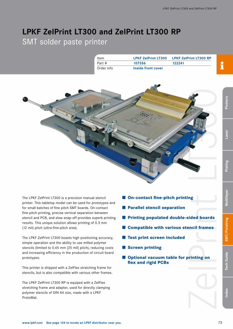
ZelP
rint L
T300
73www.lpkf.com See page 124 to locate an LPKF distributor near you.
Plot
ters
Lase
rPl
atin
gSM
T/Fi
nish
ing
Tech
Gui
deIn
dex
Mul
tila
yer
LPKF ZelPrint LT300 and ZelPrint LT300 RP SMT solder paste printer
LPKF ZelPrint LT300 and ZelPrint LT300 RP
The LPKF ZelPrint LT300 is a precision manual stencil printer. This tabletop model can be used for prototypes and for small batches of fine pitch SMT boards. On-contact fine-pitch printing, precise vertical separation between stencil and PCB, and slow snap-off provides superb printing results. This unique solution allows printing of 0.3 mm (�� mil) pitch (ultra-fine-pitch area).
The LPKF ZelPrint LT300 boasts high positioning accuracy, simple operation and the ability to use milled polymer stencils (limited to 0.65 mm [�5 mil] pitch), reducing costs and increasing efficiency in the production of circuit board prototypes.
This printer is shipped with a ZelFlex stretching frame for stencils, but is also compatible with various other frames.
The LPKF ZelPrint LT300 RP is equiped with a ZelFlex stretching frame and adapter, used for directly clamping polymer stencils of DIN A4 size, made with a LPKF ProtoMat.
On-contact fine-pitch printing
Parallel stencil separation
Printing populated double-sided boards
Compatible with various stencil frames
Test print screen included
Screen printing
Optional vacuum table for printing on flex and rigid PCBs
Item LPKF ZelPrint LT300 LPKF ZelPrint LT300 RPPart # 107356 122241Order info Inside front cover
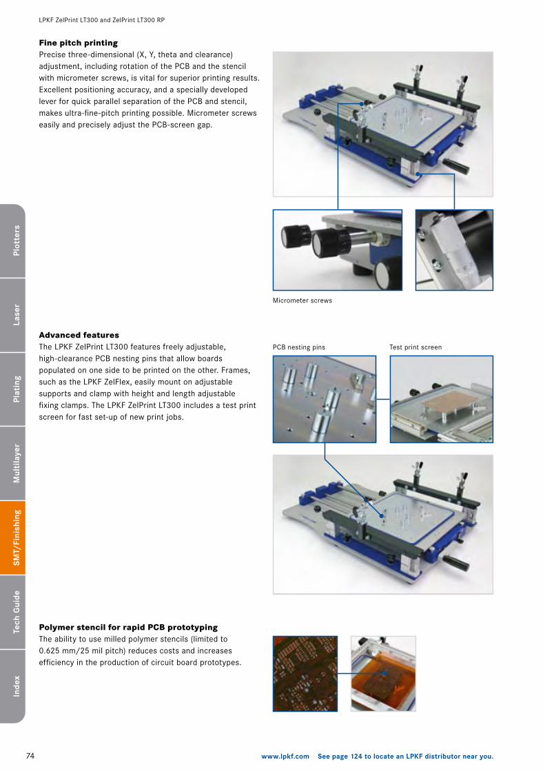
74 www.lpkf.com See page 124 to locate an LPKF distributor near you.
Plot
ters
Lase
rPl
atin
gSM
T/Fi
nish
ing
Tech
Gui
deIn
dex
Mul
tila
yer
LPKF ZelPrint LT300 and ZelPrint LT300 RP
Fine pitch printing Precise three-dimensional (X, Y, theta and clearance) adjustment, including rotation of the PCB and the stencil with micrometer screws, is vital for superior printing results. Excellent positioning accuracy, and a specially developed lever for quick parallel separation of the PCB and stencil, makes ultra-fine-pitch printing possible. Micrometer screws easily and precisely adjust the PCB-screen gap.
Advanced featuresThe LPKF ZelPrint LT300 features freely adjustable, high-clearance PCB nesting pins that allow boards populated on one side to be printed on the other. Frames, such as the LPKF ZelFlex, easily mount on adjustable supports and clamp with height and length adjustable fixing clamps. The LPKF ZelPrint LT300 includes a test print screen for fast set-up of new print jobs.
Micrometer screws
Test print screenPCB nesting pins
Polymer stencil for rapid PCB prototypingThe ability to use milled polymer stencils (limited to 0.6�5 mm/�5 mil pitch) reduces costs and increases efficiency in the production of circuit board prototypes.
75www.lpkf.com See page 124 to locate an LPKF distributor near you.
Plot
ters
Lase
rPl
atin
gSM
T/Fi
nish
ing
Tech
Gui
deIn
dex
Mul
tila
yer
LPKF ZelPrint LT300 and ZelPrint LT300 RP
Vacuum tableVacuum table for printing on flex and rigid PCBs as well as for fast clamping of rigid PCBs is available as an option. Flex and rigid boards can be easily moved to the LPKF ProtoPlace together with a vacuum table as �00% compatibility is ensured. The table can be easily and freely moved from one device to another without disconnection or interruption of vacuum.
Accessories
Accessories
Mechanical stretching frameInsert plastic or metal stencils into double-sided LPKF ZelFlex ZR frames. The fast exchange and patented stretching system optimizes tensioning and easy handling.
Part #
Type
Print area
Foil size
Squeegee max.
101321
�-sided mechanical
�60 x 330 mm (�0.�” x �3”)
Up to 3�0 x 4�0 mm (��.�” x �6.�”)
�80 mm (��”)
* incl. with delivery Specifications subject to change.
ZelFlex ZR 362x480*
ZelFlex Frames for LPKF ZelPrint LT300
Pneumatic stretching frameProfessional quick-release stencil frame with pneumatic 4-side action: Ideal for high-volume environments. Frame maintains tension even after air is disconnected.
Part #
Type
Print area
Foil size
Squeegee max.
115629
4-sided pneumatic
�86 x 388 mm (��.3” x �5.3”)
37� x 473 mm (�4.6” x �8.6”)
300 mm (��”)
Specifications subject to change.
ZelFlex Z4P 406x508x25 slim
Options
Mechanical stretching frameLPKF ZelFlex ZR �66 x 380 is specialy designed for DIN A4 polymer stencils.
Part #
Type
Print area
Foil size
Squeegee max.
122261
double-sided quick release frame
�64 x �30 mm (6.5” x 9.�”)
Up to ��4 x 3�0 mm (8,4” x ��.�”)
�80 mm (7.�”)
Specifications subject to change.
ZelFlex 266x380 with adapter
Further stretching frames upon request!
Part #
Max. PCB size
Max. air pressure
Operating pressure
Air consumption
119684
��9 x �79 mm (9” x ��”)
7 bar (�0� psi)
�.7–6 bar (�4.7–87 psi)
0.3–0.79 l/s
Specifications subject to change.
Vacuum table
ZelFlex Frames for LPKF ZelPrint LT300 RP
Special perforated ceramic printing plate is also available as option for vacuum table to move assembled flex boards into reflow oven.
Further information upon request!
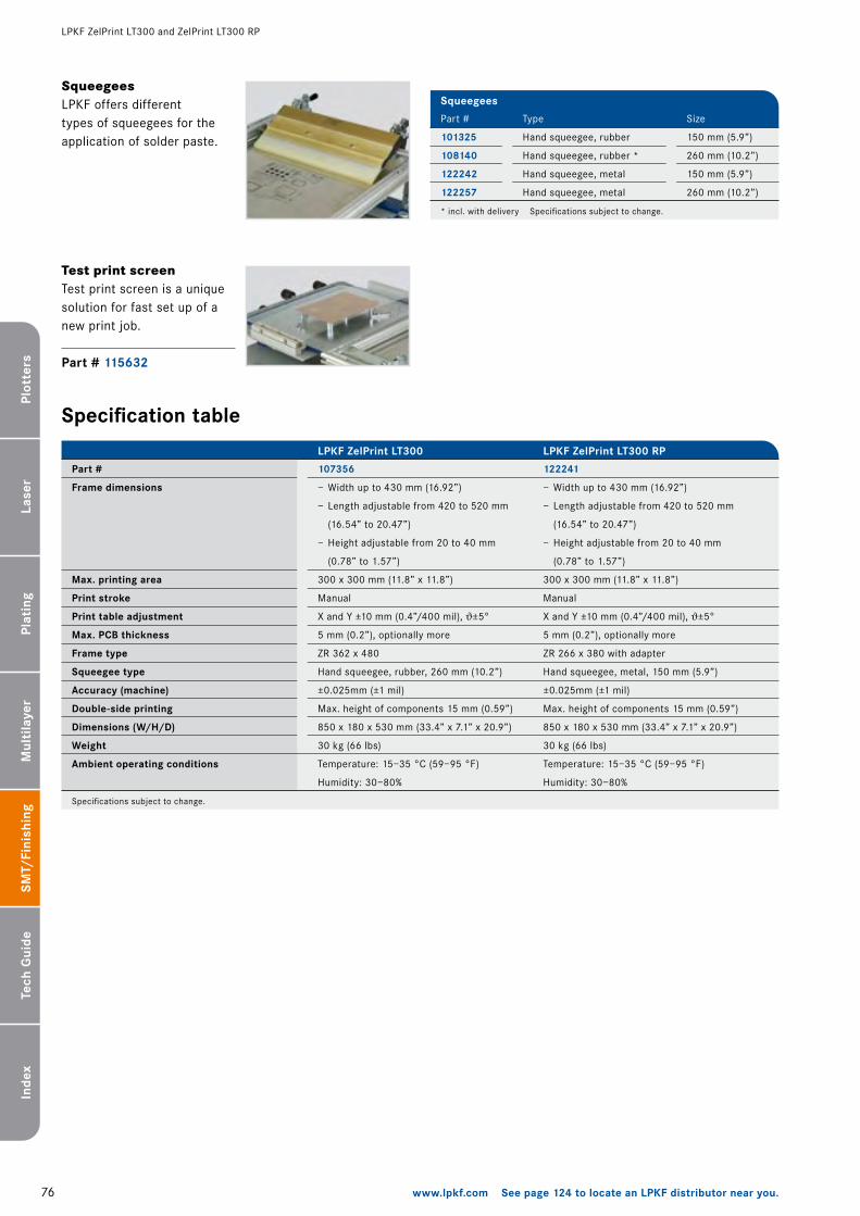
76 www.lpkf.com See page 124 to locate an LPKF distributor near you.
Plot
ters
Lase
rPl
atin
gSM
T/Fi
nish
ing
Tech
Gui
deIn
dex
Mul
tila
yer
Part #
Frame dimensions
Max. printing area
Print stroke
Print table adjustment
Max. PCB thickness
Frame type
Squeegee type
Accuracy (machine)
Double-side printing
Dimensions (W/H/D)
Weight
Ambient operating conditions
107356
– Width up to 430 mm (�6.9�”)
– Length adjustable from 4�0 to 5�0 mm
(�6.54” to �0.47”)
– Height adjustable from �0 to 40 mm
(0.78” to �.57”)
300 x 300 mm (��.8” x ��.8”)
Manual
X and Y ±�0 mm (0.4”/400 mil), ±5°
5 mm (0.�”), optionally more
ZR 36� x 480
Hand squeegee, rubber, �60 mm (�0.�”)
±0.0�5mm (±� mil)
Max. height of components �5 mm (0.59”)
850 x �80 x 530 mm (33.4” x 7.�” x �0.9”)
30 kg (66 lbs)
Temperature: �5–35 °C (59–95 °F)
Humidity: 30–80%
Specification table
Specifications subject to change.
LPKF ZelPrint LT300 and ZelPrint LT300 RP
SqueegeesLPKF offers different types of squeegees for the application of solder paste. 101325
108140
122242
122257
Hand squeegee, rubber
Hand squeegee, rubber *
Hand squeegee, metal
Hand squeegee, metal
* incl. with delivery Specifications subject to change.
Squeegees
Part # Type Size
�50 mm (5.9”)
�60 mm (�0.�”)
�50 mm (5.9”)
�60 mm (�0.�”)
Test print screenTest print screen is a unique solution for fast set up of a new print job.
Part # 115632
LPKF ZelPrint LT300 LPKF ZelPrint LT300 RP
122241
– Width up to 430 mm (�6.9�”)
– Length adjustable from 4�0 to 5�0 mm
(�6.54” to �0.47”)
– Height adjustable from �0 to 40 mm
(0.78” to �.57”)
300 x 300 mm (��.8” x ��.8”)
Manual
X and Y ±�0 mm (0.4”/400 mil), ±5°
5 mm (0.�”), optionally more
ZR �66 x 380 with adapter
Hand squeegee, metal, �50 mm (5.9”)
±0.0�5mm (±� mil)
Max. height of components �5 mm (0.59”)
850 x �80 x 530 mm (33.4” x 7.�” x �0.9”)
30 kg (66 lbs)
Temperature: �5–35 °C (59–95 °F)
Humidity: 30–80%
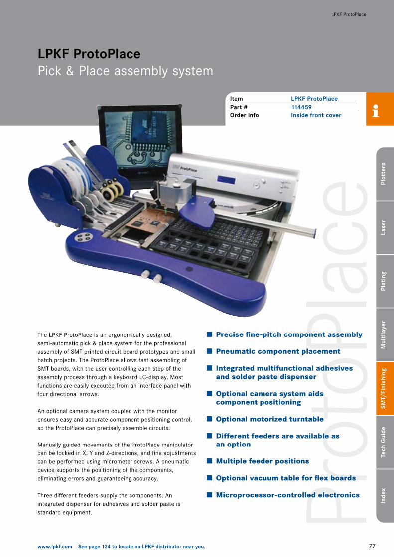
Prot
oPla
ce
77www.lpkf.com See page 124 to locate an LPKF distributor near you.
Plot
ters
Lase
rPl
atin
gSM
T/Fi
nish
ing
Tech
Gui
deIn
dex
Mul
tila
yer
LPKF ProtoPlace
LPKF ProtoPlace Pick & Place assembly system
Item LPKF ProtoPlacePart # 114459Order info Inside front cover
The LPKF ProtoPlace is an ergonomically designed, semi-automatic pick & place system for the professional assembly of SMT printed circuit board prototypes and small batch projects. The ProtoPlace allows fast assembling of SMT boards, with the user controlling each step of the assembly process through a keyboard LC-display. Most functions are easily executed from an interface panel with four directional arrows.
An optional camera system coupled with the monitor ensures easy and accurate component positioning control, so the ProtoPlace can precisely assemble circuits.
Manually guided movements of the ProtoPlace manipulator can be locked in X, Y and Z-directions, and fine adjustments can be performed using micrometer screws. A pneumatic device supports the positioning of the components, eliminating errors and guaranteeing accuracy.
Three different feeders supply the components. An integrated dispenser for adhesives and solder paste is standard equipment.
Precise fine-pitch component assembly
Pneumatic component placement
Integrated multifunctional adhesives and solder paste dispenser Optional camera system aids component positioning
Optional motorized turntable
Different feeders are available as an option
Multiple feeder positions
Optional vacuum table for flex boards
Microprocessor-controlled electronics
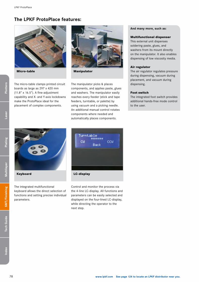
78 www.lpkf.com See page 124 to locate an LPKF distributor near you.
Plot
ters
Lase
rPl
atin
gSM
T/Fi
nish
ing
Tech
Gui
deIn
dex
Mul
tila
yer
LPKF ProtoPlace
LC-display
Control and monitor the process via the 4-line LC-display. All functions and parameters can be easily selected and displayed on the four-lined LC-display, while directing the operator to the next step.
Multifunctional dispenser This external unit dispenses soldering paste, glues, and washers from its mount directly on the manipulator. It also enables dispensing of low viscosity media.
Keyboard
The integrated multifunctional keyboard allows the direct selection of functions and setting precise individual parameters.
Air regulatorThe air regulator regulates pressure during dispensing, vacuum during placement, and vacuum during dispensing.
Micro-table
The micro-table clamps printed circuit boards as large as �97 x 4�0 mm (��.8” x �6.5”). A fine-adjustment capability and X- and Y-axis lockdowns make the ProtoPlace ideal for the placement of complex components.
Manipulator
The manipulator picks & places components, and applies paste, glues and washers. The manipulator easily reaches every feeder (stick and tape feeders, turntable, or palette) by using vacuum and a picking needle. An additional manual control rotates components where needed and automatically places components.
And many more, such as:
Foot switchThe integrated foot switch provides additional hands-free mode control to the user.
The LPKF ProtoPlace features:
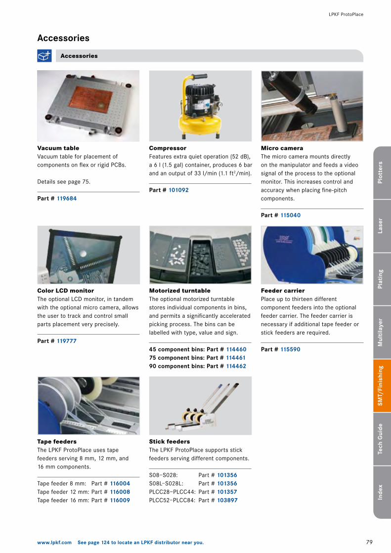
79www.lpkf.com See page 124 to locate an LPKF distributor near you.
Plot
ters
Lase
rPl
atin
gSM
T/Fi
nish
ing
Tech
Gui
deIn
dex
Mul
tila
yer
LPKF ProtoPlace
Accessories
Accessories
Motorized turntableThe optional motorized turntable stores individual components in bins, and permits a significantly accelerated picking process. The bins can be labelled with type, value and sign.
45 component bins: Part # 11446075 component bins: Part # 11446190 component bins: Part # 114462
Feeder carrierPlace up to thirteen different component feeders into the optional feeder carrier. The feeder carrier is necessary if additional tape feeder or stick feeders are required.
Part # 115590
Micro cameraThe micro camera mounts directly on the manipulator and feeds a video signal of the process to the optional monitor. This increases control and accuracy when placing fine-pitch components.
Part # 115040
Color LCD monitorThe optional LCD monitor, in tandem with the optional micro camera, allows the user to track and control small parts placement very precisely.
Part # 119777
Tape feedersThe LPKF ProtoPlace uses tape feeders serving 8 mm, �� mm, and �6 mm components.
Tape feeder 8 mm: Part # 116004Tape feeder �� mm: Part # 116008Tape feeder �6 mm: Part # 116009
CompressorFeatures extra quiet operation (5� dB), a 6 l (�.5 gal) container, produces 6 bar and an output of 33 l/min (�.� ft�/min).
Part # 101092
Stick feedersThe LPKF ProtoPlace supports stick feeders serving different components.
S08–S0�8: Part # 101356S08L–S0�8L: Part # 101356PLCC�8–PLCC44: Part # 101357PLCC5�–PLCC84: Part # 103897
Vacuum tableVacuum table for placement of components on flex or rigid PCBs. Details see page 75.
Part # 119684
80 www.lpkf.com See page 124 to locate an LPKF distributor near you.
Plot
ters
Lase
rPl
atin
gSM
T/Fi
nish
ing
Tech
Gui
deIn
dex
Mul
tila
yer
Part #
Maximum PCB size
Minimum size of components
Pulse/pause duration
Number of dosing points
Dosing quantity
Turntable position
Feeders position
Operating air pressure
Vacuum
Weight
Dimensions (W/H/D)
(w/ all feeders and turntable)
Dimensions (W/H/D)
(bare machine)
Ambient operating conditions
Compressed air supply
Power supply
114459
�97 x 4�0 mm (��.8” x �6.5”)
0�0� chip components
0.�–9 sec/0.�–� sec
Up to 300 per minute
Min. 0.� µliters
Left and/or back
Left
0.�–4 bar (�.4–58 psi)
Max. 0.8 bar (��.6 psi)
�5–35 kg (55–77 lbs) depending on accessories
�.000 x 500 x 900 mm (40” x �0” x 35”)
760 x �50 x 760 mm (30” x �0” x 30”)
Temperature: �5–35 °C (59–95 °F)
Humidity: 30–80%
6 bar (87 psi), min. �0 l/min (0.35 cfm), oil free, water free
��5/�30 V, 50–60 Hz, �0 W
LPKF ProtoPlace
Specification table
Specifications subject to change.
LPKF ProtoPlace
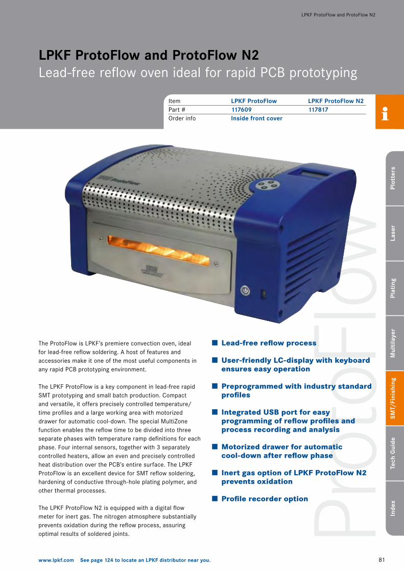
Prot
oFlo
w
8�www.lpkf.com See page 124 to locate an LPKF distributor near you.
Plot
ters
Lase
rPl
atin
gSM
T/Fi
nish
ing
Tech
Gui
deIn
dex
Mul
tila
yer
LPKF ProtoFlow and ProtoFlow N�
LPKF ProtoFlow and ProtoFlow N2 Lead-free reflow oven ideal for rapid PCB prototyping
The ProtoFlow is LPKF’s premiere convection oven, ideal for lead-free reflow soldering. A host of features and accessories make it one of the most useful components in any rapid PCB prototyping environment.
The LPKF ProtoFlow is a key component in lead-free rapid SMT prototyping and small batch production. Compact and versatile, it offers precisely controlled temperature/time profiles and a large working area with motorized drawer for automatic cool-down. The special MultiZone function enables the reflow time to be divided into three separate phases with temperature ramp definitions for each phase. Four internal sensors, together with 3 separately controlled heaters, allow an even and precisely controlled heat distribution over the PCB’s entire surface. The LPKF ProtoFlow is an excellent device for SMT reflow soldering, hardening of conductive through-hole plating polymer, and other thermal processes.
The LPKF ProtoFlow N� is equipped with a digital flow meter for inert gas. The nitrogen atmosphere substantially prevents oxidation during the reflow process, assuring optimal results of soldered joints.
Lead-free reflow process
User-friendly LC-display with keyboard ensures easy operation
Preprogrammed with industry standard profiles
Integrated USB port for easy programming of reflow profiles and process recording and analysis
Motorized drawer for automatic cool-down after reflow phase
Inert gas option of LPKF ProtoFlow N2 prevents oxidation
Profile recorder option
Item LPKF ProtoFlow LPKF ProtoFlow N2Part # 117609 117817Order info Inside front cover
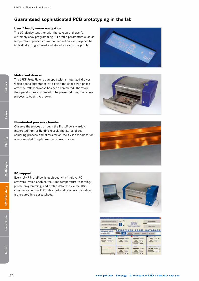
8� www.lpkf.com See page 124 to locate an LPKF distributor near you.
Plot
ters
Lase
rPl
atin
gSM
T/Fi
nish
ing
Tech
Gui
deIn
dex
Mul
tila
yer
LPKF ProtoFlow and ProtoFlow N�
Guaranteed sophisticated PCB prototyping in the lab
User friendly menu navigationThe LC-display together with the keyboard allows for extremely easy programming. All profile parameters such as temperature, process duration, and reflow ramp-up can be individually programmed and stored as a custom profile.
Motorized drawerThe LPKF ProtoFlow is equipped with a motorized drawer which opens automatically to begin the cool-down phase after the reflow process has been completed. Therefore, the operator does not need to be present during the reflow process to open the drawer.
PC supportEvery LPKF ProtoFlow is equipped with intuitive PC software, which enables real-time temperature recording, profile programming, and profile database via the USB communication port. Profile chart and temperature values are created in a spreatsheet.
Illuminated process chamberObserve the process through the ProtoFlow’s window. Integrated interior lighting reveals the status of the soldering process and allows for on-the-fly job modification where needed to optimize the reflow process.
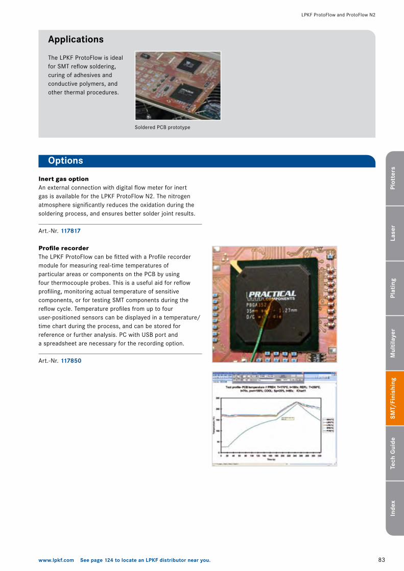
83www.lpkf.com See page 124 to locate an LPKF distributor near you.
Plot
ters
Lase
rPl
atin
gSM
T/Fi
nish
ing
Tech
Gui
deIn
dex
Mul
tila
yer
Soldered PCB prototype
Applications
The LPKF ProtoFlow is ideal for SMT reflow soldering, curing of adhesives and conductive polymers, and other thermal procedures.
LPKF ProtoFlow and ProtoFlow N�
Inert gas optionAn external connection with digital flow meter for inert gas is available for the LPKF ProtoFlow N�. The nitrogen atmosphere significantly reduces the oxidation during the soldering process, and ensures better solder joint results.
Art.-Nr. 117817
Profile recorderThe LPKF ProtoFlow can be fitted with a Profile recorder module for measuring real-time temperatures of particular areas or components on the PCB by using four thermocouple probes. This is a useful aid for reflow profiling, monitoring actual temperature of sensitive components, or for testing SMT components during the reflow cycle. Temperature profiles from up to four user-positioned sensors can be displayed in a temperature/time chart during the process, and can be stored for reference or further analysis. PC with USB port and a spreadsheet are necessary for the recording option.
Art.-Nr. 117850
Options
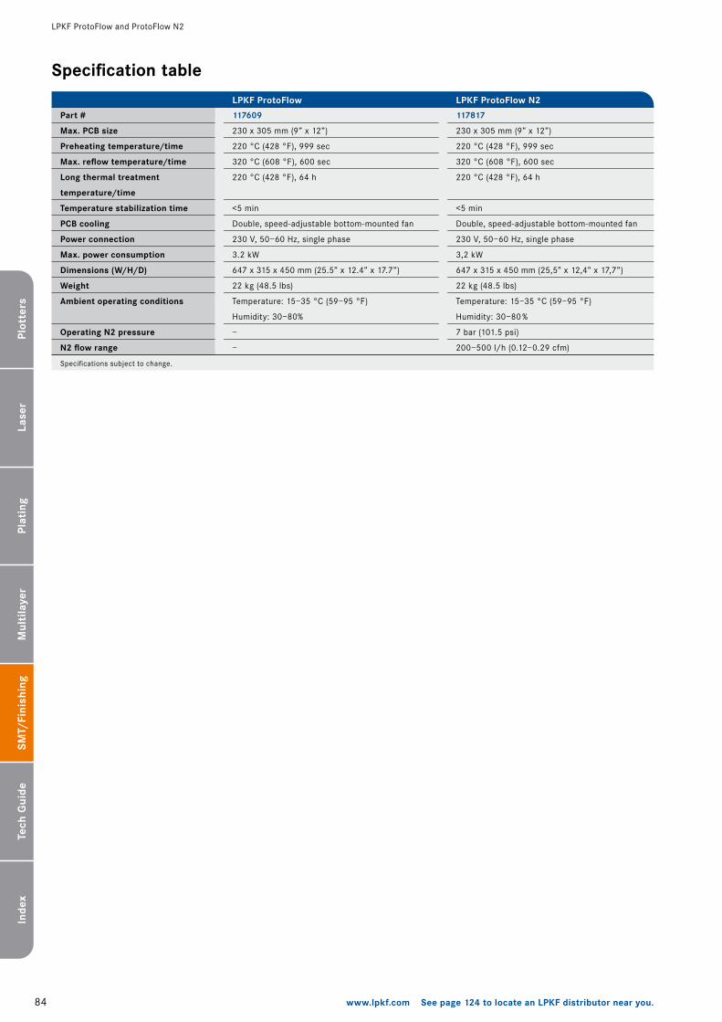
84 www.lpkf.com See page 124 to locate an LPKF distributor near you.
Plot
ters
Lase
rPl
atin
gSM
T/Fi
nish
ing
Tech
Gui
deIn
dex
Mul
tila
yer
LPKF ProtoFlow and ProtoFlow N�
Part #
Max. PCB size
Preheating temperature/time
Max. reflow temperature/time
Long thermal treatment
temperature/time
Temperature stabilization time
PCB cooling
Power connection
Max. power consumption
Dimensions (W/H/D)
Weight
Ambient operating conditions
Operating N2 pressure
N2 flow range
117609
�30 x 305 mm (9” x ��”)
��0 °C (4�8 °F), 999 sec
3�0 °C (608 °F), 600 sec
��0 °C (4�8 °F), 64 h
<5 min
Double, speed-adjustable bottom-mounted fan
�30 V, 50–60 Hz, single phase
3.� kW
647 x 3�5 x 450 mm (�5.5” x ��.4” x �7.7”)
�� kg (48.5 lbs)
Temperature: �5–35 °C (59–95 °F)
Humidity: 30–80%
–
–
Specification table
Specifications subject to change.
LPKF ProtoFlow LPKF ProtoFlow N2
117817
�30 x 305 mm (9” x ��”)
��0 °C (4�8 °F), 999 sec
3�0 °C (608 °F), 600 sec
��0 °C (4�8 °F), 64 h
<5 min
Double, speed-adjustable bottom-mounted fan
�30 V, 50–60 Hz, single phase
3,� kW
647 x 3�5 x 450 mm (�5,5” x ��,4” x �7,7”)
�� kg (48.5 lbs)
Temperature: �5–35 °C (59–95 °F)
Humidity: 30–80 %
7 bar (�0�.5 psi)
�00–500 l/h (0.��–0.�9 cfm)
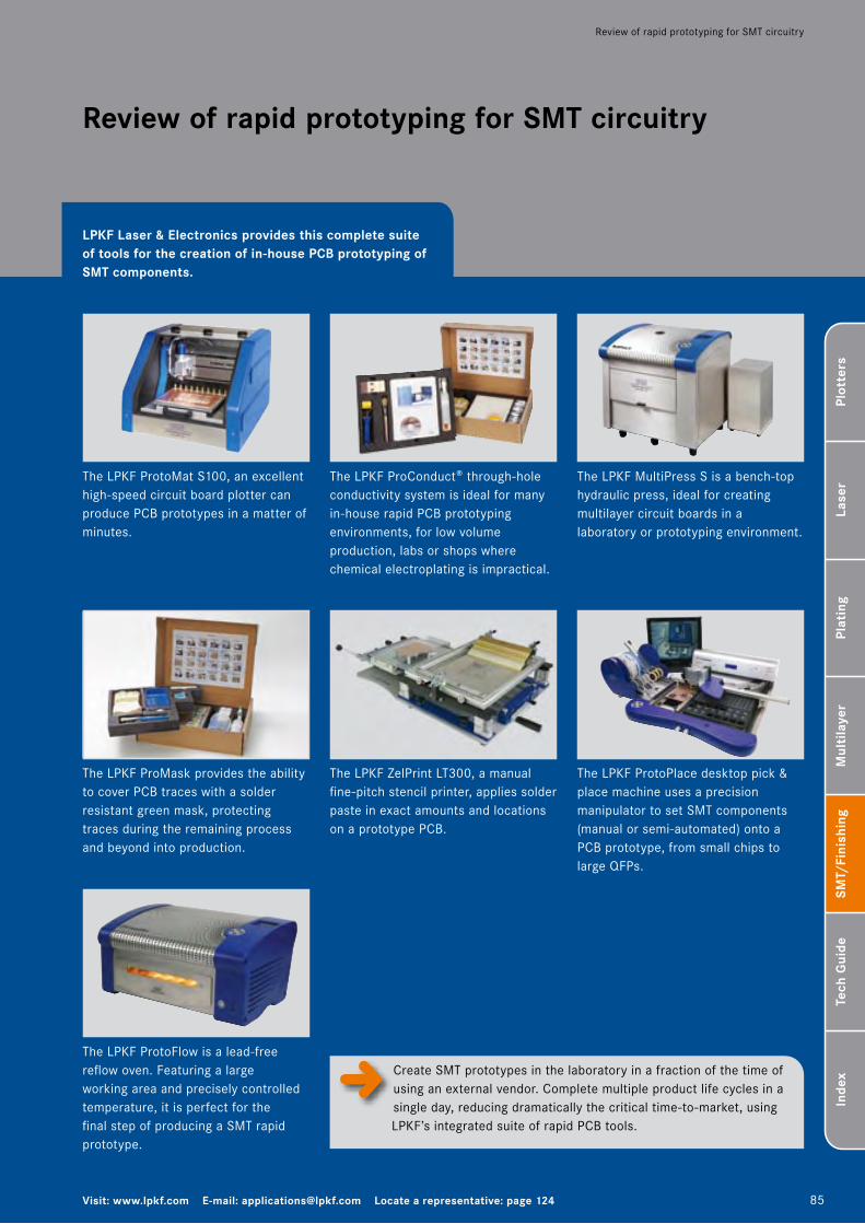
85Visit: www.lpkf.com E-mail: [email protected] Locate a representative: page 124
Plot
ters
Lase
rPl
atin
gSM
T/Fi
nish
ing
Tech
Gui
deIn
dex
Mul
tila
yer
Review of rapid prototyping for SMT circuitry
LPKF Laser & Electronics provides this complete suite of tools for the creation of in-house PCB prototyping of SMT components.
Review of rapid prototyping for SMT circuitry
The LPKF ProtoMat S�00, an excellent high-speed circuit board plotter can produce PCB prototypes in a matter of minutes.
The LPKF ProMask provides the ability to cover PCB traces with a solder resistant green mask, protecting traces during the remaining process and beyond into production.
The LPKF ZelPrint LT300, a manual fine-pitch stencil printer, applies solder paste in exact amounts and locations on a prototype PCB.
The LPKF ProtoPlace desktop pick & place machine uses a precision manipulator to set SMT components (manual or semi-automated) onto a PCB prototype, from small chips to large QFPs.
The LPKF ProtoFlow is a lead-free reflow oven. Featuring a large working area and precisely controlled temperature, it is perfect for the final step of producing a SMT rapid prototype.
The LPKF ProConduct® through-hole conductivity system is ideal for many in-house rapid PCB prototyping environments, for low volume production, labs or shops where chemical electroplating is impractical.
The LPKF MultiPress S is a bench-top hydraulic press, ideal for creating multilayer circuit boards in a laboratory or prototyping environment.
Create SMT prototypes in the laboratory in a fraction of the time of using an external vendor. Complete multiple product life cycles in a single day, reducing dramatically the critical time-to-market, using LPKF’s integrated suite of rapid PCB tools.

86 www.lpkf.com See page 124 to locate an LPKF distributor near you.
Customer statements
Working in development presents several problems when prototyping circuits.
In our situation developing a prototype circuit card is usually an on demand situation (spur of the moment) that at times we would have to complete by utilizing wire wrap, or bread boarding from a schematic.
Most of the time being a long and drawn out project with sometimes mixed results, and depending on the size of the circuit, a pain to rework.
In this situation utilizing our ProtoMat H100 system we can produce a more reliable circuit card that is easily reproducible in a matter of hours instead of days with minimal user input once the process is started, and easily support our on demand style work atmosphere.
Thanks,Michael
Michael S. BaranowskiTechnical SpecialistGeneral Dynamics Land SystemsUSA We are a small research and development lab,
so the purchase of our S62 demanded a large commitment from our operational budget. However the results have been all I could have asked for; we have total control of project scheduling. Depending on the scale our engineer can design, test and re-implement a board in 2–3 days, where before he would be at the mercy of the priorities of an outsource. Having an in-house PC Board plotter has allowed us to focus on design problems rather than the ‘hurry up and wait’ problems of scheduling issues. Greg FordGregory Industrial Computer ltd.Canada
Our customers are our best salesmen!
The LPKF ProtoMat is small and easy to use.It is very useful to make all kinds of small-series PCBs. And it corresponds fast to design changes! DENSO CORPORATION, Development DivisionMr. Tomokazu WatanabeJapan

87www.lpkf.com See page 124 to locate an LPKF distributor near you.
Customer statements
Higher educational research often demands repeated creation of new and improved prototypes. The Institute of Biomedical Engineering at the University of New Brunswick, Fredericton, N.B., Canada, has a long history in the research and clinical aspects of advanced myoelectric controls systems for artificial limbs, and it’s recognized worldwide for this work.
“The design and fabrication of prototypes is a key element of much of this research, and it is here that we utilize the ProtoMat S62”, says chief technologist John Hayden. He looked to the S62 because of the increasing demands placed on board production by surface-mount components. He also indicated that some designs were using the minimum isolation width to keep board size to a minimum.
Research that uses RF layout for wireless bio sensors will be one of the projects tackled in the near future.
John HaydenInstitute of Biomedical EngineeringUniversity of New BrunswickCanada
Being a small company, sales is always pressuring us to get out new products. With the ProtoMat M60, we are literally able to prototype our design the very next day. This better enables us to meet our deadlines, keep the sales´ folk happy and most importantly satisfy our customers. It is a great machine and so is the customers service! Shane De Lima, R&D EngineerThe Bodine CompanyColliervilleUSA
You can’t beat the performance of an LPKF system for RF & Microwave prototyping. We do up to three iterations of design within a day. Leonard WeberAgilentSanta Rosa, CAUSA
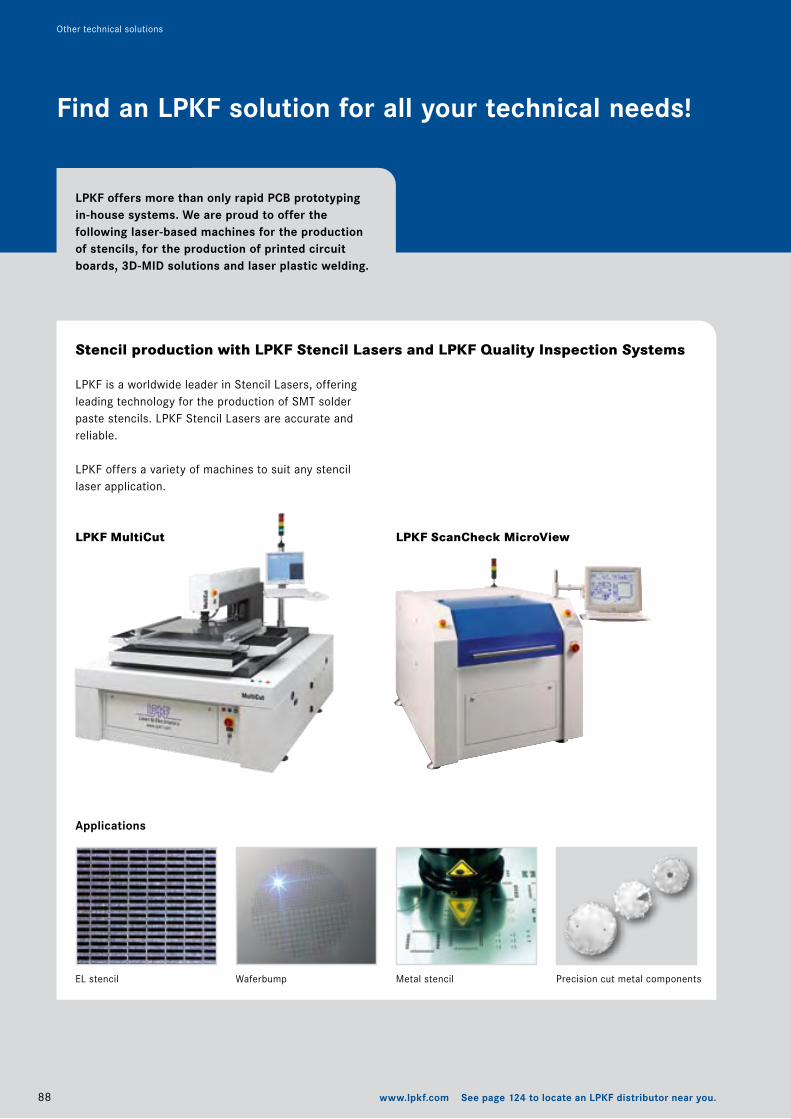
88 www.lpkf.com See page 124 to locate an LPKF distributor near you.
Find an LPKF solution for all your technical needs!
Other technical solutions
Stencil production with LPKF Stencil Lasers and LPKF Quality Inspection Systems
LPKF MultiCut LPKF ScanCheck MicroView
EL stencil Waferbump Metal stencil Precision cut metal components
Applications
LPKF is a worldwide leader in Stencil Lasers, offering leading technology for the production of SMT solder paste stencils. LPKF Stencil Lasers are accurate and reliable.
LPKF offers a variety of machines to suit any stencil laser application.
LPKF offers more than only rapid PCB prototyping in-house systems. We are proud to offer the following laser-based machines for the production of stencils, for the production of printed circuit boards, 3D-MID solutions and laser plastic welding.
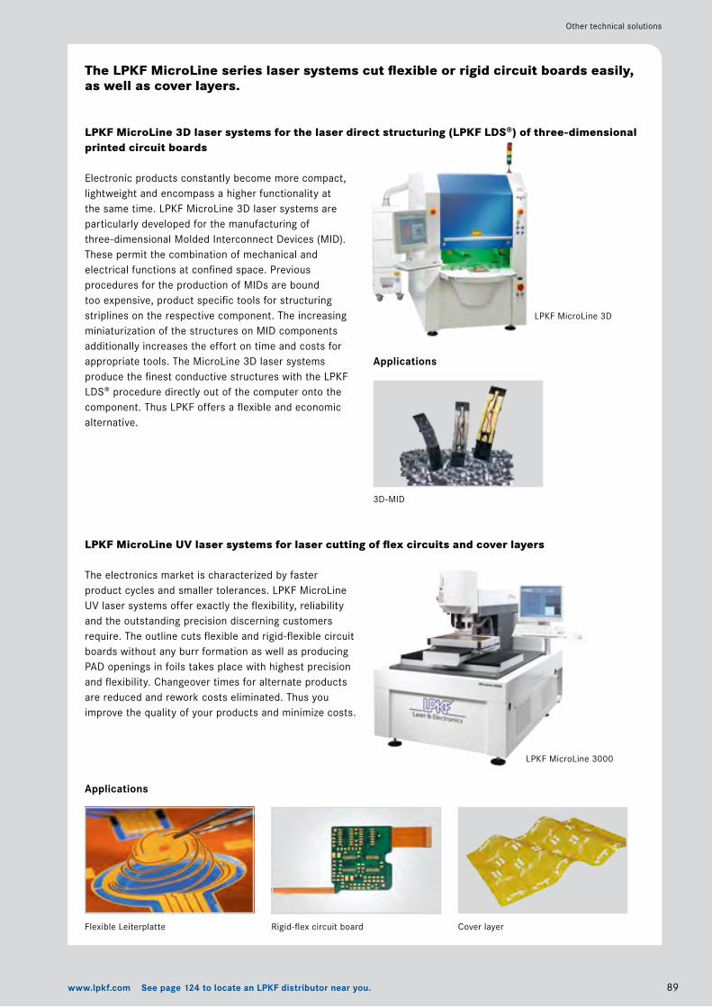
89www.lpkf.com See page 124 to locate an LPKF distributor near you.
Other technical solutions
Electronic products constantly become more compact, lightweight and encompass a higher functionality at the same time. LPKF MicroLine 3D laser systems are particularly developed for the manufacturing of three-dimensional Molded Interconnect Devices (MID). These permit the combination of mechanical and electrical functions at confined space. Previous procedures for the production of MIDs are bound too expensive, product specific tools for structuring striplines on the respective component. The increasing miniaturization of the structures on MID components additionally increases the effort on time and costs for appropriate tools. The MicroLine 3D laser systems produce the finest conductive structures with the LPKF LDS® procedure directly out of the computer onto the component. Thus LPKF offers a flexible and economic alternative.
LPKF MicroLine UV laser systems for laser cutting of flex circuits and cover layers
Flexible Leiterplatte Rigid-flex circuit board Cover layer
Applications
LPKF MicroLine 3000
The LPKF MicroLine series laser systems cut flexible or rigid circuit boards easily, as well as cover layers.
3D-MID
LPKF MicroLine 3D laser systems for the laser direct structuring (LPKF LDS®) of three-dimensional printed circuit boards
LPKF MicroLine 3D
Applications
The electronics market is characterized by faster product cycles and smaller tolerances. LPKF MicroLine UV laser systems offer exactly the flexibility, reliability and the outstanding precision discerning customers require. The outline cuts flexible and rigid-flexible circuit boards without any burr formation as well as producing PAD openings in foils takes place with highest precision and flexibility. Changeover times for alternate products are reduced and rework costs eliminated. Thus you improve the quality of your products and minimize costs.
90 www.lpkf.com See page 124 to locate an LPKF distributor near you.
Other technical solutions
Laser plastics welding offers many technological as well as economic advantages over conventional welding procedures. The Plastics Welding Division of LPKF Laser & Electronics AG is one of the first business ventures in the world to exclusively concentrate on this innovative technology, offering simple economic solutions for any set of requirements.
For more information please contact:
LPKF Laser & Electronics AGPlastic Welding DivisionGundstraße �5D-9�056 ErlangenGermany
Phone +49-(0)9�3�-6�657-�0Fax +49-(0)9�3�-6�657-77E-mail [email protected] www.laserquipment.de
LPKF laser plastics welding
LPKF MicroLine 350Ci
LPKF MicroLine CO2 laser system for laser depaneling of rigid circuit boards.
Depanelization of assembled PCBs
Electronic devices are constantly getting smaller and more sensitive. For depanelization it is essential to reduce influencing forces to a minimum. At the same time the requirements increase for precision and speed. With modern laser technology the LPKF MicroLine CO� laser sytems handle these technological hurdles for depanelization of assembled panels. Any forms can be cut fast and economically without mechanical stress. Electronic devices can be placed very near to the PCBs edge, so the electronic developer’s benefits from the greatest possible design freedom.
Applications
9�www.lpkf.com See page 124 to locate an LPKF distributor near you.
Comprehensive job shop service in Laser-micro-machining LaserMicronics GmbH, Germany, offers a comprehensive job shop, focusing on micromachining and material processing by industrial lasers. LaserMicronics enjoys full access to LPKF’s laser systems as well as other top-of-the-line prototyping systems, and is also capable of both small batch and high volume production (in close cooperation with LPKF System customers).
LaserMicronics is an innovative pioneer in process development providing a powerful knowledge base for nearly all high-end applications. LaserMicronics strictly exercises the demands of the DIN EN ISO 900�:�000 at both production facilities in Garbsen and Erlangen, Germany.
For more information please contact:
LaserMicronics GmbHOsteriede 7D-308�7 GarbsenGermany
Phone +49-(0)5�3�-7095-0Fax +49-(0)5�3�-7095-90E-mail [email protected] www.lasermicronics.de
LPKF’s comprehensive job shop serves the needs of the laser micromachining industry
LPKF Motion & Control GmbH, a subsidiary of LPKF Laser & Electronics, develops and manufactures innovative drive and motion control technology, providing products such as precision drives, granite based air-guided systems with linear or spindle drives, highly mobile single and multi-dimensional linear induction motors, position measuring systems and interpolators, 3D measuring systems and modern control systems and servo controls.
For more information please contact:
LPKF Motion & Control GmbHMittelbergstraße �7D-985�7 SuhlGermany
Phone +49-(0)368�-89�4-0Fax +49-(0)368�-89�4-44E-mail [email protected] www.lpkf-mc.de
Innovative motion control, precision drive technology, portal and measuring systems
Otherr technical solutions
9� www.lpkf.com See page 124 to locate an LPKF distributor near you.
Plot
ters
Lase
rPl
atin
gSM
T/Fi
nish
ing
Tech
Gui
deIn
dex
Mul
tila
yer
Technical Guide
The following technical information demonstrates simply and clearly the different manufacturing steps to produce single-sided, double-sided and Multilayer printed circuit boards using LPKF Rapid PCB Prototyping systems. Simple handling of the machines, and procedures for the production of complex printed circuit boards, create a lasting first impression of the systems. At the same time, clearly defined system functions and features specify which machines and procedures can be selected for different applications.
Basic knowledge printed circuit boards . . . 93Basic data to the selection of the correct machine and procedure. . . . . . . . . . . . . . . . . 94Differences in the production of multilayer . . . . . . . . . . . . . . . . . . . . . . . . . . . . 96Data preparation with LPKF software LPKF CircuitCAM. . . . . . . . . . . . . . . . . . . . 98 LPKF BoardMaster . . . . . . . . . . . . . . . . . 100Milling . . . . . . . . . . . . . . . . . . . . . . . . . . . . . . 102Bonding multilayer . . . . . . . . . . . . . . . . . . . . 104Marking and drilling . . . . . . . . . . . . . . . . . . . 106Through-hole conductivity without chemicals . . . . . . . . . . . . . . . . . . . . . . . . . . . 107Galvanic through-hole plating . . . . . . . . . . 108Solder-resist masks, legend printing. . . . . .110Solder paste printing . . . . . . . . . . . . . . . . . . .111Assembling . . . . . . . . . . . . . . . . . . . . . . . . . . .112Plumbiferous and lead-free reflow soldering . . . . . . . . . . . . . . . . . . . . . . . . . . . . .113Applications . . . . . . . . . . . . . . . . . . . . . . . . . .114Cross Reference List . . . . . . . . . . . . . . . . . . .117
Contents
Technical GuideIntroduction
LPKF circuit board plottersThe LPKF ProtoMat series applies standards in precision, flexibility and ease-of-use. By structuring the printed circuit board, LPKF circuit board plotters form the heart of rapid PCB prototyping. They shorten the manufacturing time of PCB prototypes and substantially reduce time-to-market for new designs. The high-speed spindles (4�,000–�00,000 rpm), resolution (up to 0.�5 µm (0.0� mil), and high repeatability ensure extremely precise production of the finest structures needed in RF and microwave applications. The various working areas and motor speeds of the LPKF
Please note, this technical information does not replace the manual for the respective product.
ProtoMat models can help dictate the correct machine for each application in regards to both technological and economic feasibility.
Multilayer and through-hole platingThe production of high-quality Multilayer printed circuit boards with LPKF Rapid PCB Prototyping systems is fast and simple. The LPKF MultiPress S bonds the different layers of a multilayer PCB. The LPKF ProConduct® provides conductivity without chemical processing. For galvanic systems, LPKF provides the Contac RS and MiniContac RS.
SoftwareEvery LPKF ProtoMat circuit board plotter ships with a comprehensive software suite; LPKF CircuitCAM and the control software LPKF BoardMaster. Both programs are easy to operate and simple to learn. CircuitCAM imports CAD data from Gerber®, GerberX, HP-GL™, Excellon®, Sieb & Meier, Barco® and ODB++®. The data is modified directly on the production level. LPKF BoardMaster imports the production data (LMD files) of CircuitCAM or HP-GL™ data, and controls the LPKF ProtoMat circuit board plotters. With the WYSIWYG software, modifications of the graphic data are done simply and comfortably – duplication, rotation, tiling etc.
SMT prototypingLPKF offers a number of useful tools for the in-house production of SMT prototypes. The LPKF ProMask® for solder-resist masks and legend printing. The LPKF ZelPrint LT300 applies solder paste or adhesive on the PCB. Our LPKF ProtoPlace utilizes a semi-automatic placing technique for SMT components, while the LPKF ProtoFlow allows for a controlled reflow soldering. You will find an easy-to-use machine or procedure for all your SMT needs. With fast, simple, and safe techniques you will save valuable time in the production development process.
Further/special applicationsLPKF circuit board plotters structure not only printed circuit boards fast and accurately, but are also used for different applications.
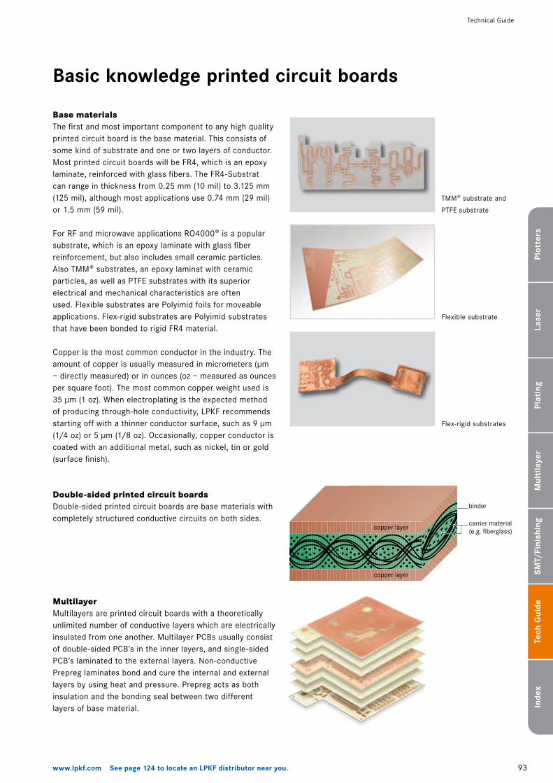
copper layer
copper layer
binder
carrier material(e.g. fiberglass)
93www.lpkf.com See page 124 to locate an LPKF distributor near you.
Plot
ters
Lase
rPl
atin
gSM
T/Fi
nish
ing
Tech
Gui
deIn
dex
Mul
tila
yer
Technical Guide
Basic knowledge printed circuit boards
Double-sided printed circuit boardsDouble-sided printed circuit boards are base materials with completely structured conductive circuits on both sides.
Base materialsThe first and most important component to any high quality printed circuit board is the base material. This consists of some kind of substrate and one or two layers of conductor. Most printed circuit boards will be FR4, which is an epoxy laminate, reinforced with glass fibers. The FR4-Substrat can range in thickness from 0.�5 mm (�0 mil) to 3.��5 mm (��5 mil), although most applications use 0.74 mm (�9 mil) or �.5 mm (59 mil).
For RF and microwave applications RO4000® is a popular substrate, which is an epoxy laminate with glass fiber reinforcement, but also includes small ceramic particles. Also TMM® substrates, an epoxy laminat with ceramic particles, as well as PTFE substrates with its superior electrical and mechanical characteristics are often used. Flexible substrates are Polyimid foils for moveable applications. Flex-rigid substrates are Polyimid substrates that have been bonded to rigid FR4 material.
Copper is the most common conductor in the industry. The amount of copper is usually measured in micrometers (µm – directly measured) or in ounces (oz – measured as ounces per square foot). The most common copper weight used is 35 µm (� oz). When electroplating is the expected method of producing through-hole conductivity, LPKF recommends starting off with a thinner conductor surface, such as 9 µm (�/4 oz) or 5 µm (�/8 oz). Occasionally, copper conductor is coated with an additional metal, such as nickel, tin or gold (surface finish).
MultilayerMultilayers are printed circuit boards with a theoretically unlimited number of conductive layers which are electrically insulated from one another. Multilayer PCBs usually consist of double-sided PCB’s in the inner layers, and single-sided PCB’s laminated to the external layers. Non-conductive Prepreg laminates bond and cure the internal and external layers by using heat and pressure. Prepreg acts as both insulation and the bonding seal between two different layers of base material.
TMM® substrate and
PTFE substrate
Flexible substrate
Flex-rigid substrates
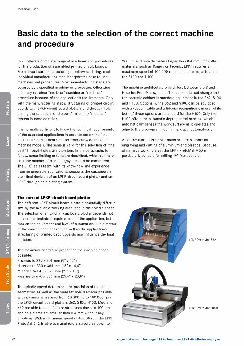
94 www.lpkf.com See page 124 to locate an LPKF distributor near you.
Plot
ters
Lase
rPl
atin
gSM
T/Fi
nish
ing
Tech
Gui
deIn
dex
Mul
tila
yer
Technical Guide
Basic data to the selection of the correct machine and procedure
LPKF offers a complete range of machines and procedures for the production of assembled printed circuit boards. From circuit surface structuring to reflow soldering, each individual manufacturing step incorporates easy-to-use machines and procedures. Most manufacturing steps are covered by a specified machine or procedure. Otherwise it is easy to select “the best” machine or “the best” procedure because of the application’s requirements. Only with the manufacturing steps, structuring of printed circuit boards with LPKF circuit board plotters and through-hole plating the selection “of the best” machine/”the best” system is more complex.
It is normally sufficient to know the technical requirements of the expected applications in order to determine “the best” LPKF circuit board plotter from our wide range of machine models. The same is valid for the selection of “the best“ through-hole plating system. In the paragraphs to follow, some limiting criteria are described, which can help limit the number of machines/systems to be considered. The LPKF sales team, with its know-how and experience from innumerable applications, supports the customers in their final decision of an LPKF circuit board plotter and an LPKF through hole plating system.
The correct LPKF circuit board plotterThe different LPKF circuit board plotters essentially differ in size by the available working area, and in the spindle speed. The selection of an LPKF circuit board plotter depends not only on the technical requirements of the application, but also on the equipment and level of automation. It is a matter of the convenience desired, as well as the applications structuring of printed circuit boards may influence the final decision.
The maximum board size predefines the machine series possible:S-series to ��9 x 305 mm (9” x ��”)H-series to 380 x 365 mm (�5” x �4,4”)M-series to 540 x 375 mm (��” x �5”)X-series to 650 x 530 mm (�5,6” x �0,8”)
The spindle speed determines the precision of the circuit geometries as well as the smallest hole diameter possible. With its maximum speed from 60,000 up to �00,000 rpm the LPKF circuit board plotters S6�, S�00, H�00, M60 and X60 are able to manufacture structures down to �00 µm and hole diameters smaller than 0.4 mm without any problems. With a maximum speed of 4�,000 rpm the LPKF ProtoMat S4� is able to manufacture structures down to
�00 µm and hole diameters larger than 0.4 mm. For softer materials, such as Rogers or Taconic, LPKF requires a maximum speed of �00,000 rpm spindle speed as found on the S�00 and H�00.
The machine architecture only differs between the S and H-series ProtoMat systems. The automatic tool change and the acoustic cabinet is standard equipment in the S6�, S�00 and H�00. Optionally, the S6� and S�00 can be equipped with a vacuum table and a fiducial recognition camera, while both of those options are standard for the H�00. Only the H�00 offers the automatic depth control sensing, which automatically senses the work surface as it operates and adjusts the preprogrammed milling depth automatically.
All of the current ProtoMat machines are suitable for engraving and cutting of aluminium and plastics. Because of its large working area, the LPKF ProtoMat M60 is particularly suitable for milling �9” front panels.
LPKF ProtoMat S6�
LPKF ProtoMat H�00
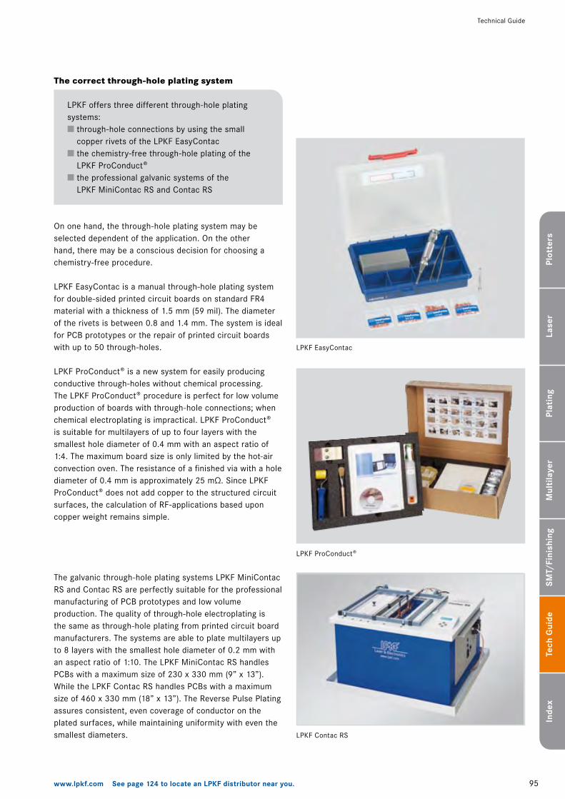
95www.lpkf.com See page 124 to locate an LPKF distributor near you.
Plot
ters
Lase
rPl
atin
gSM
T/Fi
nish
ing
Tech
Gui
deIn
dex
Mul
tila
yer
Technical Guide
On one hand, the through-hole plating system may be selected dependent of the application. On the other hand, there may be a conscious decision for choosing a chemistry-free procedure.
LPKF EasyContac is a manual through-hole plating system for double-sided printed circuit boards on standard FR4 material with a thickness of �.5 mm (59 mil). The diameter of the rivets is between 0.8 and �.4 mm. The system is ideal for PCB prototypes or the repair of printed circuit boards with up to 50 through-holes.
LPKF ProConduct® is a new system for easily producing conductive through-holes without chemical processing. The LPKF ProConduct® procedure is perfect for low volume production of boards with through-hole connections; when chemical electroplating is impractical. LPKF ProConduct® is suitable for multilayers of up to four layers with the smallest hole diameter of 0.4 mm with an aspect ratio of �:4. The maximum board size is only limited by the hot-air convection oven. The resistance of a finished via with a hole diameter of 0.4 mm is approximately �5 mΩ. Since LPKF ProConduct® does not add copper to the structured circuit surfaces, the calculation of RF-applications based upon copper weight remains simple.
The galvanic through-hole plating systems LPKF MiniContac RS and Contac RS are perfectly suitable for the professional manufacturing of PCB prototypes and low volume production. The quality of through-hole electroplating is the same as through-hole plating from printed circuit board manufacturers. The systems are able to plate multilayers up to 8 layers with the smallest hole diameter of 0.� mm with an aspect ratio of �:�0. The LPKF MiniContac RS handles PCBs with a maximum size of �30 x 330 mm (9” x �3”). While the LPKF Contac RS handles PCBs with a maximum size of 460 x 330 mm (�8” x �3”). The Reverse Pulse Plating assures consistent, even coverage of conductor on the plated surfaces, while maintaining uniformity with even the smallest diameters.
LPKF EasyContac
LPKF ProConduct®
LPKF Contac RS
LPKF offers three different through-hole plating systems: through-hole connections by using the small copper rivets of the LPKF EasyContac the chemistry-free through-hole plating of the LPKF ProConduct® the professional galvanic systems of the LPKF MiniContac RS and Contac RS
The correct through-hole plating system
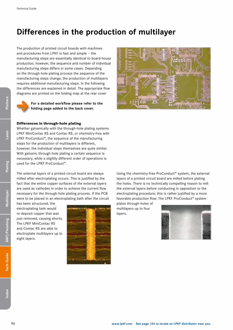
96 www.lpkf.com See page 124 to locate an LPKF distributor near you.
Plot
ters
Lase
rPl
atin
gSM
T/Fi
nish
ing
Tech
Gui
deIn
dex
Mul
tila
yer
Technical Guide
Differences in the production of multilayer
The production of printed circuit boards with machines and procedures from LPKF is fast and simple – the manufacturing steps are essentially identical to board-house production, however, the sequence and number of individual manufacturing steps differs in some cases. Depending on the through-hole plating process the sequence of the manufacturing steps change; the production of multilayers requires additional manufacturing steps. In the following the differences are explained in detail. The appropriate flow diagrams are printed on the folding map at the rear cover
Differences in through-hole platingWhether galvanically with the through-hole plating systems LPKF MiniContac RS and Contac RS, or chemistry-free with LPKF ProConduct®, the sequence of the manufacturing steps for the production of multilayers is different, however, the individual steps themselves are quite similar. With galvanic through-hole plating a certain sequence is necessary, while a slightly different order of operations is used for the LPKF ProConduct®.
The external layers of a printed circuit board are always milled after electroplating occurs. This is justified by the fact that the entire copper surfaces of the external layers are used as cathodes in order to achieve the current flow necessary for the through-hole plating process. If the PCB were to be placed in an electroplating bath after the circuit has been structured, the electroplating tank would re-deposit copper that was just removed, causing shorts. The LPKF MiniContac RS and Contac RS are able to electroplate multilayers up to eight layers.
Using the chemistry-free ProConduct® system, the external layers of a printed circuit board are milled before plating the holes. There is no technically compelling reason to mill the external layers before conducting in opposition to the electroplating procedure; this is rather justified by a more favorable production flow. The LPKF ProConduct® system plates through-holes of multilayers up to four layers.
For a detailed workflow please refer to the folding page added to the back cover.
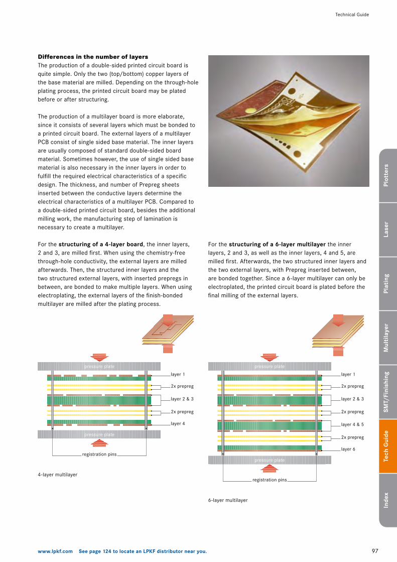
layer 1
layer 4
2x prepreg
2x prepreg
pressure plate
pressure plate
registration pins
layer 2 & 3
97www.lpkf.com See page 124 to locate an LPKF distributor near you.
Plot
ters
Lase
rPl
atin
gSM
T/Fi
nish
ing
Tech
Gui
deIn
dex
Mul
tila
yer
Technical Guide
Differences in the number of layersThe production of a double-sided printed circuit board is quite simple. Only the two (top/bottom) copper layers of the base material are milled. Depending on the through-hole plating process, the printed circuit board may be plated before or after structuring.
The production of a multilayer board is more elaborate, since it consists of several layers which must be bonded to a printed circuit board. The external layers of a multilayer PCB consist of single sided base material. The inner layers are usually composed of standard double-sided board material. Sometimes however, the use of single sided base material is also necessary in the inner layers in order to fulfill the required electrical characteristics of a specific design. The thickness, and number of Prepreg sheets inserted between the conductive layers determine the electrical characteristics of a multilayer PCB. Compared to a double-sided printed circuit board, besides the additional milling work, the manufacturing step of lamination is necessary to create a multilayer.
For the structuring of a 6-layer multilayer the inner layers, � and 3, as well as the inner layers, 4 and 5, are milled first. Afterwards, the two structured inner layers and the two external layers, with Prepreg inserted between, are bonded together. Since a 6-layer multilayer can only be electroplated, the printed circuit board is plated before the final milling of the external layers.
For the structuring of a 4-layer board, the inner layers, � and 3, are milled first. When using the chemistry-free through-hole conductivity, the external layers are milled afterwards. Then, the structured inner layers and the two structured external layers, with inserted prepregs in between, are bonded to make multiple layers. When using electroplating, the external layers of the finish-bonded multilayer are milled after the plating process.
4-layer multilayer
6-layer multilayer
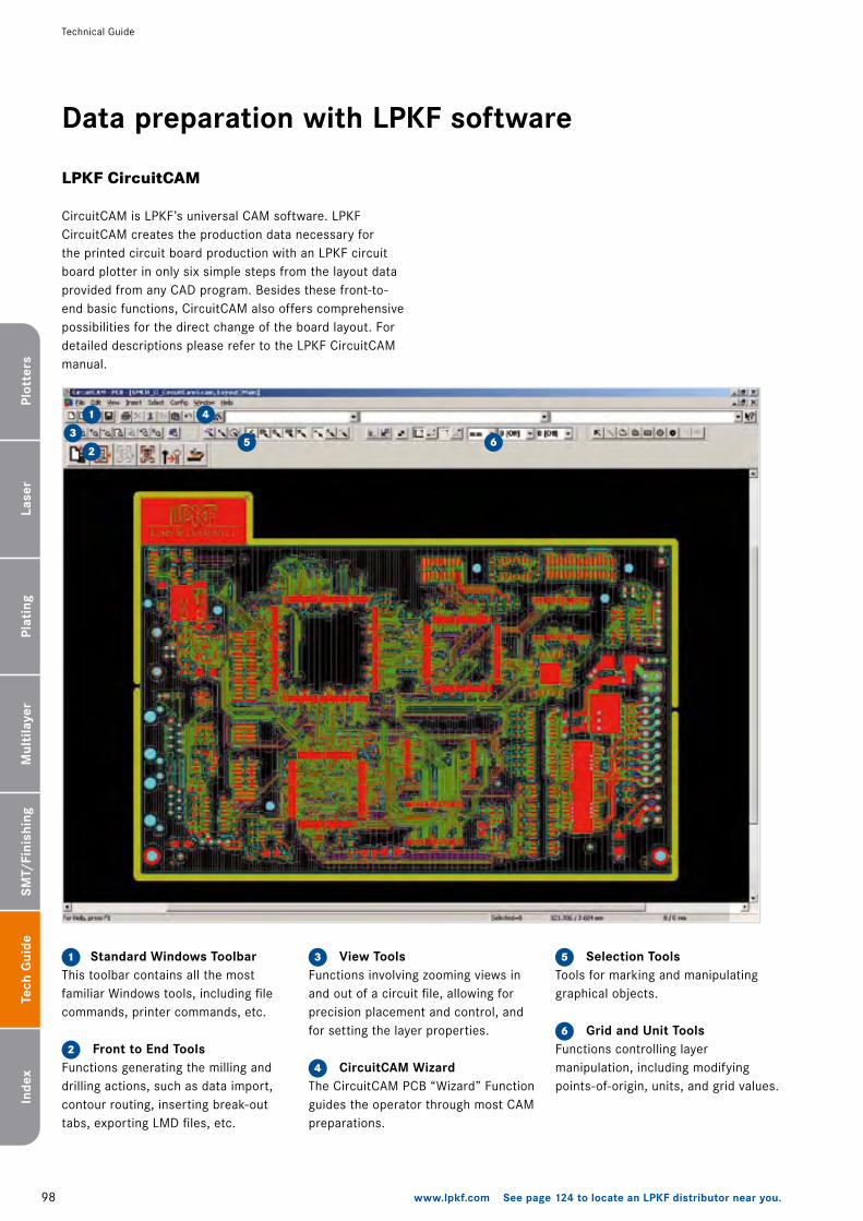
1
3
4
5 6
2
3
4
5
6
1
2
98 www.lpkf.com See page 124 to locate an LPKF distributor near you.
Plot
ters
Lase
rPl
atin
gSM
T/Fi
nish
ing
Tech
Gui
deIn
dex
Mul
tila
yer
Technical Guide
Data preparation with LPKF software
LPKF CircuitCAM
CircuitCAM is LPKF’s universal CAM software. LPKF CircuitCAM creates the production data necessary for the printed circuit board production with an LPKF circuit board plotter in only six simple steps from the layout data provided from any CAD program. Besides these front-to-end basic functions, CircuitCAM also offers comprehensive possibilities for the direct change of the board layout. For detailed descriptions please refer to the LPKF CircuitCAM manual.
Selection ToolsTools for marking and manipulating graphical objects.
CircuitCAM WizardThe CircuitCAM PCB “Wizard” Function guides the operator through most CAM preparations.
Standard Windows ToolbarThis toolbar contains all the most familiar Windows tools, including file commands, printer commands, etc.
Front to End ToolsFunctions generating the milling and drilling actions, such as data import, contour routing, inserting break-out tabs, exporting LMD files, etc.
View ToolsFunctions involving zooming views in and out of a circuit file, allowing for precision placement and control, and for setting the layer properties. Grid and Unit Tools
Functions controlling layer manipulation, including modifying points-of-origin, units, and grid values.
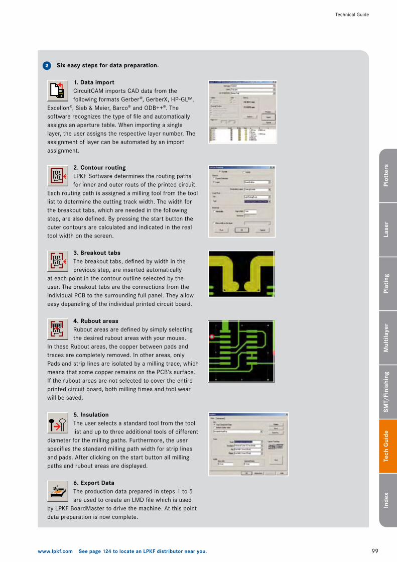
2
99www.lpkf.com See page 124 to locate an LPKF distributor near you.
Plot
ters
Lase
rPl
atin
gSM
T/Fi
nish
ing
Tech
Gui
deIn
dex
Mul
tila
yer
Technical Guide
1. Data importCircuitCAM imports CAD data from the following formats Gerber®, GerberX, HP-GL™,
Excellon®, Sieb & Meier, Barco® and ODB++®. The software recognizes the type of file and automatically assigns an aperture table. When importing a single layer, the user assigns the respective layer number. The assignment of layer can be automated by an import assignment.
2. Contour routingLPKF Software determines the routing paths for inner and outer routs of the printed circuit.
Each routing path is assigned a milling tool from the tool list to determine the cutting track width. The width for the breakout tabs, which are needed in the following step, are also defined. By pressing the start button the outer contours are calculated and indicated in the real tool width on the screen.
3. Breakout tabsThe breakout tabs, defined by width in the previous step, are inserted automatically
at each point in the contour outline selected by the user. The breakout tabs are the connections from the individual PCB to the surrounding full panel. They allow easy depaneling of the individual printed circuit board.
4. Rubout areasRubout areas are defined by simply selecting the desired rubout areas with your mouse.
In these Rubout areas, the copper between pads and traces are completely removed. In other areas, only Pads and strip lines are isolated by a milling trace, which means that some copper remains on the PCB’s surface. If the rubout areas are not selected to cover the entire printed circuit board, both milling times and tool wear will be saved.
5. InsulationThe user selects a standard tool from the tool list and up to three additional tools of different
diameter for the milling paths. Furthermore, the user specifies the standard milling path width for strip lines and pads. After clicking on the start button all milling paths and rubout areas are displayed.
6. Export DataThe production data prepared in steps � to 5 are used to create an LMD file which is used
by LPKF BoardMaster to drive the machine. At this point data preparation is now complete.
Six easy steps for data preparation.
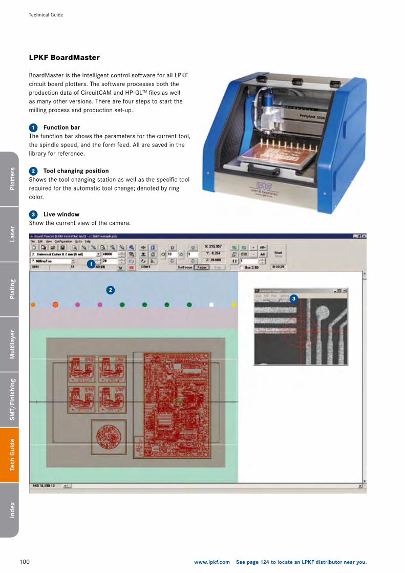
1
2
3
1
2
3
�00 www.lpkf.com See page 124 to locate an LPKF distributor near you.
Plot
ters
Lase
rPl
atin
gSM
T/Fi
nish
ing
Tech
Gui
deIn
dex
Mul
tila
yer
Technical Guide
LPKF BoardMaster
BoardMaster is the intelligent control software for all LPKF circuit board plotters. The software processes both the production data of CircuitCAM and HP-GLTM files as well as many other versions. There are four steps to start the milling process and production set-up.
Function barThe function bar shows the parameters for the current tool, the spindle speed, and the form feed. All are saved in the library for reference.
Tool changing positionShows the tool changing station as well as the specific tool required for the automatic tool change; denoted by ring color.
Live windowShow the current view of the camera.
Four easy steps how to start the milling process and therefore the production.
�0�www.lpkf.com See page 124 to locate an LPKF distributor near you.
Plot
ters
Lase
rPl
atin
gSM
T/Fi
nish
ing
Tech
Gui
deIn
dex
Mul
tila
yer
Technical Guide
1. Specify base material The base material is placed in the working area of the circuit board plotter. The user moves the milling head towards two opposite corners of the base material and trains these points. As a result, the size and the position of the base material are specified automatically and displayed on the computer screen.
2. Data importThe production data provided by LPKF CircuitCAM or HP-GLTM data are imported. BoardMaster places the data in the center of the base material. The tool lists are taken over automatically. The data of several printed circuit boards can then be imported in succession.
3. PositioningThe printed circuit board data is moved and rotated on the base material either graphically by mouse or positioned by feeding specific coordinates into the software. It is very simple to create a step-and-repeat array, as only the number of individual PCBs and the desired distance between each PCB is needed.
4. ManufacturingBoardMaster processes the control data and optimizes the milling process in regards to the runtime, number of tool changes and drill wear. All tool parameters such as feed rate and spindle speeds are saved in the library, so that intervention by the operator is not necessary. LPKF circuit board plotters with a fully loaded automatic tool bar can easily be started by pressing the start/stop button. LPKF circuit board plotters without automatic tool change will prompt the operator to insert the requested tool.
�0� www.lpkf.com See page 124 to locate an LPKF distributor near you.
Plot
ters
Lase
rPl
atin
gSM
T/Fi
nish
ing
Tech
Gui
deIn
dex
Mul
tila
yer
Technical Guide
Milling
Milling is the actual heart of the rapid PCB prototyping process. The milling process transfers the printed circuit board layout of the outer and inner layers to the base material. The conductive coating is removed from the insulating layer. The drill shavings are extracted directly at the milling head by a vacuum system.
The easy to use LPKF circuit board plotters enable straightforward production of complex printed circuit boards without specialized user knowledge. The automation level of the milling process depends on the particular LPKF circuit board plotter model used. Options such as the vacuum table or the fiducial recognition camera additionally facilitate easy operation and reduce operator interaction to a minimum.
The milling spindle motor dictates the maximum speed required for creating the most accurate structures and smallest hole diameters possible. Therefore, the higher the spindle speed the smaller the tools that can be used. Softer base materials, for example HF-applications require a higher spindle speed as well.
Some milling tools for the structuring of printed circuit boards are provided with a conical tip. By adjusting the milling depth into the base material at the beginning of every milling process, not only the milling width, but also the minimum insulation distances are determined. During the milling process, the milling head creates downward pressure on the base material. The length of the milling tool exposed beyond the milling head dictates the depth of cut, and is adjusted with a knurled thumb screw on the milling spindle; denoted as the working depth limiter. The distance ring of a milling tool can accurately be placed using the precision ring setter. Therefore the adjustment of the working depth after each tool change is no longer necessary.
All circuit traces and pads are first isolated with the standard Universal Cutter or End Mill of your choice. This guarantees both clean and accurate, exactly equal edge geometries, which positively influence the electrical characteristics of a printed circuit board. Only in areas with small insulation spaces is a smaller milling bit used. The largest possible milling tools are used to produce large rubout areas in order to save time and cost; due to the wear on smaller tools.
�03www.lpkf.com See page 124 to locate an LPKF distributor near you.
Plot
ters
Lase
rPl
atin
gSM
T/Fi
nish
ing
Tech
Gui
deIn
dex
Mul
tila
yer
Technical Guide
The life cycle of the different tools is saved by LPKF BoardMaster in the form of maximum linear distance or the maximum holes drilled. The milling distance or the number of holes drilled by the current tool is always displayed. A warning refers to an upcoming tool change. After replacing a used tool, the counter is automatically reset to 0.
The LPKF ProtoMat H�00 is equipped with an automatic depth control sensor. The air-cushioned milling head lowers the milling tool over a sensor switch which automatically sets the predefined depth that was programmed for that specific tool. Manual adjusting is thereby avoided.
The automatic tool change is a mounted magazine which holds different drilling and milling tools. It exchanges tools during the milling process which allows for unattended operation. In contrast to the manual tool change systems, the operator saves not only time, but is also relieved from having to monitor or “baby sit” the machine, waiting for the system to prompt the user for the next tool change.
The acoustic cabinet reduces the noise of the system, allowing the machine to be used in any laboratory setting. The plotter operates safely in any work environment; therefore each circuit board plotter with automatic tool change is equipped with an acoustic cabinet.
For further details please refer to the manual of the respective LPKF circuit board plotter.
�04 www.lpkf.com See page 124 to locate an LPKF distributor near you.
Plot
ters
Lase
rPl
atin
gSM
T/Fi
nish
ing
Tech
Gui
deIn
dex
Mul
tila
yer
Technical Guide
For the production of multilayers, the external layers of a printed circuit board must be bonded with the inner layers by using heat and pressure. The external layers, TopLayer and BottomLayer, are usually base materials with one conductive layer. Depending on the through-hole plating process used, the external layers are structured before or after the bonding – galvanic plating before, chemistry-free plating with LPKF ProConduct® after. The inner layers of a multilayer are mostly base materials with two conductive layers and are always structured before the bonding lamination.
The inner and external layers of a multilayer are cured by laminates without a conductive layer; called Prepreg. At the same time, the Prepreg acts as an insulator between the conductive layers. When bonding with the base material, the resin of the Prepreg becomes fluid from the high temperature press, and therefore provides an optimal connection. It is important that no bubbles between the material occur. For the best results it is necessary to adjust the correct pressure, as well as the appropriate temperature profile, depending on the specific material requirements and by the number of layers. The press temperature of a standard multilayer PCB is approximately �80 °C (356 °F).
To ensure proper flow of the melted resin, the sheets of Prepreg are cut �5 mm (0.6”) smaller than the size of the base material. This border or margin has to be taken into account while the printed circuit board is being structured (i.e. to keep free of traces and pads). Four registration pins provide the accurate adjustment of the base materials, and keep the individual layers in position during the press process. The slotted registration holes (3 x 5 mm, 0.�” x 0.�”) for mounting the base material to the pressing plates, are to be drilled at pre-defined positions.
LPKF MultiPress S bonds multilayer circuits of up to eight layers of all common rigid, rigid-flexible or flexible substrates. It delivers equal pressure on the full press plate area (��9 x 305 mm, 9” x ��”), and therefore provides homogeneous material composition. The LPKF MultiPress S can save up to nine different time/temperature/pressure profiles, which can be programmed by the push-button LC-display. Standard profiles for LPKF materials are already pre-programmed in the factory. Special process profiles also ensure the bonding of sensitive HF-materials, which require a press temperature of approximately �30 °C (446 °F). The LPKF MultiPress S guarantees optimal results with rapid heat-up times at temperatures up to �50 °C (48� °F), as well as short cooling phases by an efficient heat transmission.
Bonding multilayer
�05www.lpkf.com See page 124 to locate an LPKF distributor near you.
Plot
ters
Lase
rPl
atin
gSM
T/Fi
nish
ing
Tech
Gui
deIn
dex
Mul
tila
yer
Technical Guide
The components of a multilayer are stacked one above the other according to the respective layer structure in a special press form. Press molds and press cushions guarantee the optimal pressure distribution in the pressform. The LPKF MultiPress S, with automatic hydraulics, automatically controls the different heating and press phases of a process profile. The pressure of the LPKF MultiPress S, with hand pump, must be manually developed before each press phase, and be controlled and adjusted during the entire bonding process. LC-display messages and audio signals, prompt the user for any required action, and also provide information about the phase changes during the lamination process.
For further details please refer to the manual of the LPKF MultiPress S.
�06 www.lpkf.com See page 124 to locate an LPKF distributor near you.
Plot
ters
Lase
rPl
atin
gSM
T/Fi
nish
ing
Tech
Gui
deIn
dex
Mul
tila
yer
Technical Guide
Marking and drilling
Structuring a printed circuit board is not only isolation of the traces and pads by milling the conductive layer, but also drilling through-holes. The drill holes are needed for through-hole plating and serve as registration points or for the mounting of the printed circuit board.
All holes on a printed circuit board can be made with an LPKF circuit board plotter. Drilling tools with a diameter from 0.� to �.4 mm are available. Holes with a diameter larger than �.4 mm are routed rather than drilled. LPKF CircuitCAM software automatically converts these large drill holes to routed holes. The drilling parameters such as spindle speed and head-down time, for ProtoMat systems equipped with a motorized Z-drive, are automatically saved by the BoardMaster control software.
Very small drill bits, or drill bits that have begun to dull, may experience something known as “drill wander” in which the drill bit can be slightly deflected, causing the exit hole on the bottom side to not be completely centered to the pad. The 90° tip of the universal cutter (�/8”), which is
Cut out the printed circuit board
All LPKF circuit board plotters are suitable for the contour routing of PCBs by using the appropriate milling tools. A printed circuit board can be routed through the entire material thickness. Various styles of cut-outs or outlines can be manufactured, from circles to rectangles to complex forms. Hole diameters larger than �.4 mm are always routed rather than drilled. LPKF circuit board plotters are also suitable for depanelization: cut step-and-repeat arrays, or individual boards with different sizes and variations.
The choice of the appropriate milling tool depends on the desired milling width. Surface milling tools with a larger diameter are more stable and can therefore be driven at a higher feed rate. On the other hand, cut-through routing tools depend on the material to be worked on; FR4 material is cut through using a contour router. For soft RF base materials or aluminium, a double-edged end mill is the right choice.
For further details please refer to the manual of the respective LPKF circuit board plotter.
normally used for �00 µm isolation tracks, is the optimal tool for creating pilot holes which mark an easy entry point for the drill bit, minimizing any wander. The CAM software CircuitCAM automatically produces the appropriate production data and transfers the data to the marking drill phase of the control software LPKF BoardMaster (the operator has to adjust the appropriate penetration depth into the printed circuit board at the working depth limiter).
�07www.lpkf.com See page 124 to locate an LPKF distributor near you.
Plot
ters
Lase
rPl
atin
gSM
T/Fi
nish
ing
Tech
Gui
deIn
dex
Mul
tila
yer
Technical Guide
Through-hole conductivity without chemicals
LPKF offers two alternative procedures for the through-hole plating of PCB’s without chemicals. The LPKF EasyContac manual through-hole plating system works with copper-alloy rivets which are manually placed in the through-holes and riveted. This procedure is ideal for double layer PCBs with up to 50 through-holes.
For further details please refer to the respective manual of LPKF EasyContac or LPKF ProConduct®.
The LPKF ProConduct® through-hole conductivity system is ideal for PCB prototypes or low volume production. This chemistry-free procedure is extremely economical for a high number of through-holes, and can be used perfectly in environments with chemical restrictions. LPKF ProConduct® is suitable for multilayers up to four layers.
With use of the LPKF ProConduct® printed circuit boards are plated in eight simple steps.
1. Protective filmAfter milling and cleaning the PCB, a clear adhesive Protection Film is applied to both sides of the PCB.
2. DrillingDrill the through-holes through the Protection Film and PCB using a ProtoMat circuit board plotter.
3. Prepare vacuum tableWith a thin layer of fleece backing material protecting the vacuum table, place the PCB on the table, covering any open vacuum table surrounding the PCB with paper or plastic in order to focus the airflow through the PCB.
4. Coat page 1Knead the portioned conductive polymer packet to soften it and spread it across the entire board surface using a squeegee, making sure to fill every hole.
5. Apply suctionSwitch on the vacuum table. Continue moving the polymer over the surface with the squeegee until all of the excess paste has been drawn through the drill holes.
6. Verify and repeat for side 2Verify visually that the polymer has properly coated every hole, and repeat steps 4 and 5 on the other side of the PCB.
7. CuringCarefully remove the protective film from both sides of the PCB and cure the board for 30 minutes in a �60 °C (3�0 °F) hot air oven.
8. Final prepAfter the cooldown period, wash the board with the ProConduct® citrus cleaner to get rid of any oxidation residue. Then finally rinse the PCB with warm water.
Table top system LPKF Contac RS
�08 www.lpkf.com See page 124 to locate an LPKF distributor near you.
Plot
ters
Lase
rPl
atin
gSM
T/Fi
nish
ing
Tech
Gui
deIn
dex
Mul
tila
yer
Technical Guide
Galvanic through-hole plating
The LPKF Contac RS and MiniContac RS are electroplating systems for the professional through-hole plating of PCB prototypes and short-run production. The chemical processes are identical to professional PCB electroplating systems in everything but scale. The electroplating systems are specifically designed for ease-of-use. No particular chemistry background is necessary to operate or maintain the Contac RS or MiniContac RS systems.
There are two basic differences between the two electroplating systems; Maximum plating area: the LPKF Contac RS can process base materials up to 460 x 330 mm (�8” x �3”), while the LPKF MiniContac RS can use a base material size of up to �30 x 330 mm (9” x �3”). Secondly, there is a difference in the number of baths; the MiniContac RS is equipped with 4 chemical baths: two cleaning baths, an activator bath and a galvanic bath. While the Contac RS contains an additional bath for chemical tinning, as well as a rinsing bath with an external water connection to support the cleaning process.
LPKF has automated the plating process as much as possible, using a step-by-step menu-driven system to walk a user through every step of the process.
1. Washing and degreasingThe printed circuit board is washed and degreased in a cycle of two baths to make absolutely sure that all contaminants are cleared away, and that the electroplating process will function as cleanly as possible.
2. Activator applicationA carbon activator is applied to the printed circuit board, adhering to all surfaces designated for plating.
3. ElectroplatingThe LPKF electroplating sequence includes full digital control over the process. User interaction is kept at an absolute minimum – the PCB is simply submerged in the first bath, and the computer controls the rest of the process, notifying the user when to move the PCB to the next bath.
4. Final CleaningThe last step of the process is a final cleaning of the PCB. After the printed circuit board is dry from the final rinse, it is ready for production. The total process requires 90 to ��0 minutes.
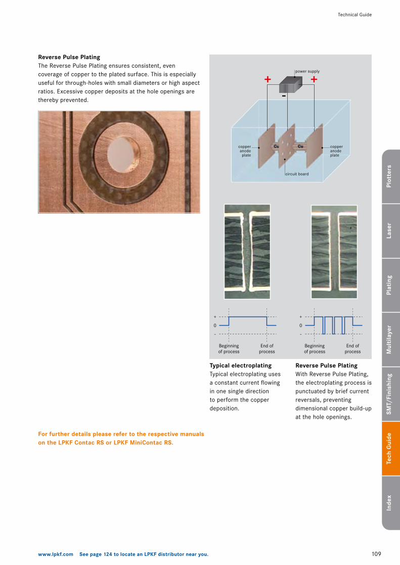
Cu Cu
circuit board
power supply
copperanodeplate
copperanodeplate
�09www.lpkf.com See page 124 to locate an LPKF distributor near you.
Plot
ters
Lase
rPl
atin
gSM
T/Fi
nish
ing
Tech
Gui
deIn
dex
Mul
tila
yer
Technical Guide
Typical electroplatingTypical electroplating uses a constant current flowing in one single direction to perform the copper deposition.
Reverse Pulse PlatingThe Reverse Pulse Plating ensures consistent, even coverage of copper to the plated surface. This is especially useful for through-holes with small diameters or high aspect ratios. Excessive copper deposits at the hole openings are thereby prevented.
For further details please refer to the respective manuals on the LPKF Contac RS or LPKF MiniContac RS.
Reverse Pulse PlatingWith Reverse Pulse Plating, the electroplating process is punctuated by brief current reversals, preventing dimensional copper build-up at the hole openings.
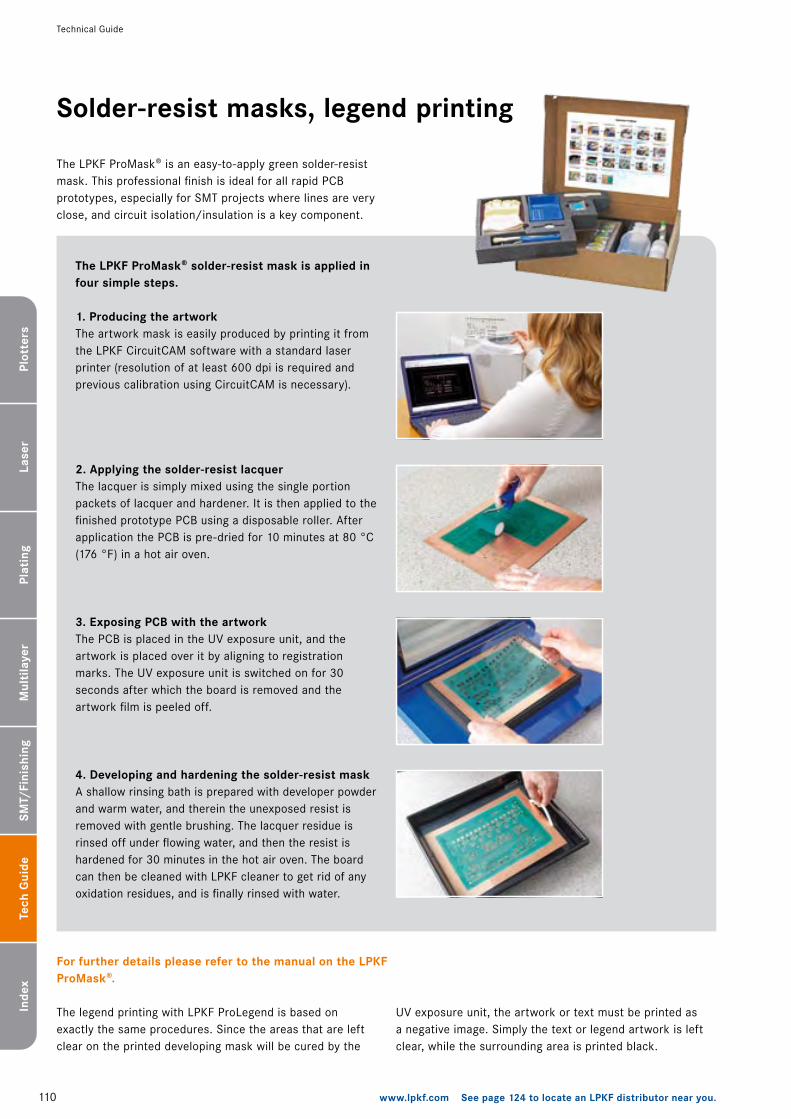
��0 www.lpkf.com See page 124 to locate an LPKF distributor near you.
Plot
ters
Lase
rPl
atin
gSM
T/Fi
nish
ing
Tech
Gui
deIn
dex
Mul
tila
yer
Technical Guide
Solder-resist masks, legend printing
The LPKF ProMask® is an easy-to-apply green solder-resist mask. This professional finish is ideal for all rapid PCB prototypes, especially for SMT projects where lines are very close, and circuit isolation/insulation is a key component.
The LPKF ProMask® solder-resist mask is applied in four simple steps.
1. Producing the artworkThe artwork mask is easily produced by printing it from the LPKF CircuitCAM software with a standard laser printer (resolution of at least 600 dpi is required and previous calibration using CircuitCAM is necessary).
2. Applying the solder-resist lacquerThe lacquer is simply mixed using the single portion packets of lacquer and hardener. It is then applied to the finished prototype PCB using a disposable roller. After application the PCB is pre-dried for �0 minutes at 80 °C (�76 °F) in a hot air oven.
3. Exposing PCB with the artworkThe PCB is placed in the UV exposure unit, and the artwork is placed over it by aligning to registration marks. The UV exposure unit is switched on for 30 seconds after which the board is removed and the artwork film is peeled off.
4. Developing and hardening the solder-resist mask A shallow rinsing bath is prepared with developer powder and warm water, and therein the unexposed resist is removed with gentle brushing. The lacquer residue is rinsed off under flowing water, and then the resist is hardened for 30 minutes in the hot air oven. The board can then be cleaned with LPKF cleaner to get rid of any oxidation residues, and is finally rinsed with water.
The legend printing with LPKF ProLegend is based on exactly the same procedures. Since the areas that are left clear on the printed developing mask will be cured by the
UV exposure unit, the artwork or text must be printed as a negative image. Simply the text or legend artwork is left clear, while the surrounding area is printed black.
For further details please refer to the manual on the LPKF ProMask®.
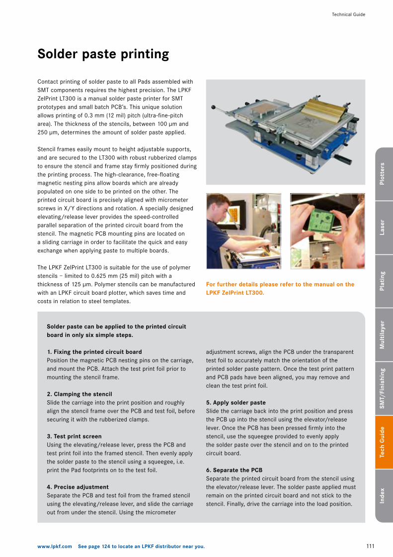
���www.lpkf.com See page 124 to locate an LPKF distributor near you.
Plot
ters
Lase
rPl
atin
gSM
T/Fi
nish
ing
Tech
Gui
deIn
dex
Mul
tila
yer
Technical Guide
Solder paste printing
Contact printing of solder paste to all Pads assembled with SMT components requires the highest precision. The LPKF ZelPrint LT300 is a manual solder paste printer for SMT prototypes and small batch PCB’s. This unique solution allows printing of 0.3 mm (�� mil) pitch (ultra-fine-pitch area). The thickness of the stencils, between �00 µm and �50 µm, determines the amount of solder paste applied.
Stencil frames easily mount to height adjustable supports, and are secured to the LT300 with robust rubberized clamps to ensure the stencil and frame stay firmly positioned during the printing process. The high-clearance, free-floating magnetic nesting pins allow boards which are already populated on one side to be printed on the other. The printed circuit board is precisely aligned with micrometer screws in X/Y directions and rotation. A specially designed elevating/release lever provides the speed-controlled parallel separation of the printed circuit board from the stencil. The magnetic PCB mounting pins are located on a sliding carriage in order to facilitate the quick and easy exchange when applying paste to multiple boards.
The LPKF ZelPrint LT300 is suitable for the use of polymer stencils – limited to 0.6�5 mm (�5 mil) pitch with a thickness of ��5 µm. Polymer stencils can be manufactured with an LPKF circuit board plotter, which saves time and costs in relation to steel templates.
For further details please refer to the manual on the LPKF ZelPrint LT300.
Solder paste can be applied to the printed circuit board in only six simple steps.
1. Fixing the printed circuit boardPosition the magnetic PCB nesting pins on the carriage, and mount the PCB. Attach the test print foil prior to mounting the stencil frame.
2. Clamping the stencilSlide the carriage into the print position and roughly align the stencil frame over the PCB and test foil, before securing it with the rubberized clamps.
3. Test print screenUsing the elevating/release lever, press the PCB and test print foil into the framed stencil. Then evenly apply the solder paste to the stencil using a squeegee, i.e. print the Pad footprints on to the test foil.
4. Precise adjustmentSeparate the PCB and test foil from the framed stencil using the elevating/release lever, and slide the carriage out from under the stencil. Using the micrometer
adjustment screws, align the PCB under the transparent test foil to accurately match the orientation of the printed solder paste pattern. Once the test print pattern and PCB pads have been aligned, you may remove and clean the test print foil.
5. Apply solder pasteSlide the carriage back into the print position and press the PCB up into the stencil using the elevator/release lever. Once the PCB has been pressed firmly into the stencil, use the squeegee provided to evenly apply the solder paste over the stencil and on to the printed circuit board.
6. Separate the PCBSeparate the printed circuit board from the stencil using the elevator/release lever. The solder paste applied must remain on the printed circuit board and not stick to the stencil. Finally, drive the carriage into the load position.
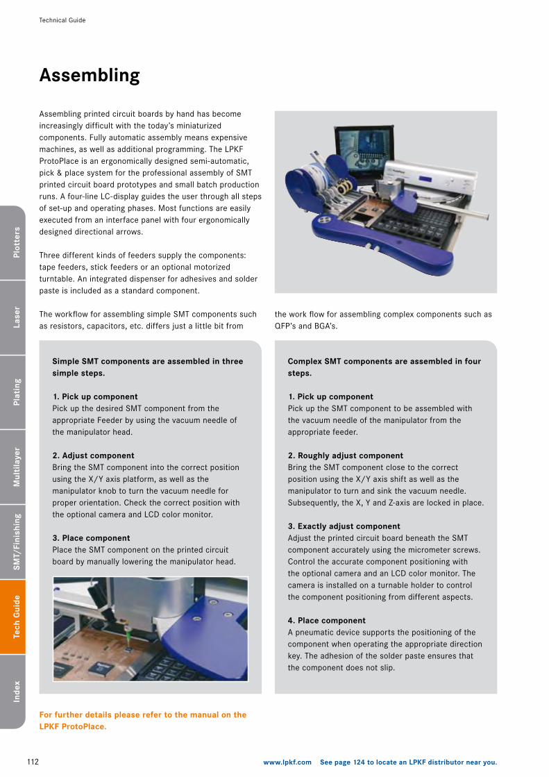
��� www.lpkf.com See page 124 to locate an LPKF distributor near you.
Plot
ters
Lase
rPl
atin
gSM
T/Fi
nish
ing
Tech
Gui
deIn
dex
Mul
tila
yer
Technical Guide
Assembling
Assembling printed circuit boards by hand has become increasingly difficult with the today’s miniaturized components. Fully automatic assembly means expensive machines, as well as additional programming. The LPKF ProtoPlace is an ergonomically designed semi-automatic, pick & place system for the professional assembly of SMT printed circuit board prototypes and small batch production runs. A four-line LC-display guides the user through all steps of set-up and operating phases. Most functions are easily executed from an interface panel with four ergonomically designed directional arrows.
Three different kinds of feeders supply the components: tape feeders, stick feeders or an optional motorized turntable. An integrated dispenser for adhesives and solder paste is included as a standard component.
The workflow for assembling simple SMT components such as resistors, capacitors, etc. differs just a little bit from
Simple SMT components are assembled in three simple steps.
1. Pick up componentPick up the desired SMT component from the appropriate Feeder by using the vacuum needle of the manipulator head.
2. Adjust componentBring the SMT component into the correct position using the X/Y axis platform, as well as the manipulator knob to turn the vacuum needle for proper orientation. Check the correct position with the optional camera and LCD color monitor.
3. Place componentPlace the SMT component on the printed circuit board by manually lowering the manipulator head.
Complex SMT components are assembled in four steps.
1. Pick up componentPick up the SMT component to be assembled with the vacuum needle of the manipulator from the appropriate feeder.
2. Roughly adjust componentBring the SMT component close to the correct position using the X/Y axis shift as well as the manipulator to turn and sink the vacuum needle. Subsequently, the X, Y and Z-axis are locked in place.
3. Exactly adjust componentAdjust the printed circuit board beneath the SMT component accurately using the micrometer screws. Control the accurate component positioning with the optional camera and an LCD color monitor. The camera is installed on a turnable holder to control the component positioning from different aspects.
4. Place componentA pneumatic device supports the positioning of the component when operating the appropriate direction key. The adhesion of the solder paste ensures that the component does not slip.
For further details please refer to the manual on the LPKF ProtoPlace.
the work flow for assembling complex components such as QFP’s and BGA’s.
��3www.lpkf.com See page 124 to locate an LPKF distributor near you.
Plot
ters
Lase
rPl
atin
gSM
T/Fi
nish
ing
Tech
Gui
deIn
dex
Mul
tila
yer
Technical Guide
Plumbiferous and lead-free reflow soldering
Reflow soldering is the last production step of the rapid PCB prototyping process. The LPKF ProtoFlow is a reflow oven which is suitable for both standard and lead-free solder pastes; RoHS compliant reflow soldering. Printed circuit boards up to �30 x 305 mm (9” x ��”) in size and a maximum temperature of 3�0 °C (608 °F) can be processed. Four internal temperature sensors together with three seperately controlled heaters provide an even and accurate temperature distribution over the entire printed circuit board surface. The inert gas option of the ProtoFlow N� enables setting and digital monitoring of the nitrogen flow. The nitrogen atmosphere significantly decreases the oxidation during the soldering process and ensures better solder joints.
Preprogrammed standard reflow profiles are installed at the factory. Further temperature/time profiles can simply be programmed and saved under an individual name using the direction keys and the four-line LC-display. With the special multi-zone function it is possible to define up to five separate phases; with a programmable temperature ramp for up to three of them. The entire soldering process is automatic and does not require user interruption. The motorized drawer opens automatically for the cool-down phase of the reflow process. The integrated lighting allows the user to supervise the soldering process through a front window panel.
The LPKF ProtoFlow can be connected to a PC using a USB interface. The intuitive PC software records the process temperature in real time and allows for profile parameters to be saved. The LPKF ProtoFlow can be fitted with four optional temperature sensors, which can be mounted anywhere on the PCB or components, allowing for a complete real time data logging of temperature profiles with instant feedback to the user. This data can be stored on a PC and analyzed at any time.
For further details please refer to the manual on the LPKF ProtoFlow.
Printed circuit boards produced and
assembled with LPKF machines and
technologies.
��4 www.lpkf.com See page 124 to locate an LPKF distributor near you.
Plot
ters
Lase
rPl
atin
gSM
T/Fi
nish
ing
Tech
Gui
deIn
dex
Mul
tila
yer
Technical Guide
Applications
Flexible/rigid-flexible printed circuit boardsFlexible and rigid-flexible printed circuit boards usually cause difficulties in handling. To fix the boards on a work surface can cause some problems. To make the handling easier almost all LPKF systems can be equipped with a vacuum table. Reason to equip the circuit board plotter with a vacuum table is not only a safer positioning of the material, it is also to make the handling of the machine faster and more simple.
Since the base material of flexible printed circuit boards is always softer, HF tools are primarily used for the milling process. Another advantage of the HF tools is that they do not penetrate deeply into the material. Structuring a flexible printed circuit board is based on the same milling process of rigid base materials.
With rigid-flexible printed circuit boards, flexible PCB’s are connected together with rigid PCB’s. The production of rigid-flexible printed circuit boards is similar to the production of multilayer boards. The rigid PCB’s are structured in a panel, the area where the flexible portion is to be inserted remains unstructured in the panel, and is covered with a protective foil. The flexible PCB is then pressed upon the already structured rigid areas. Finally, the unstructured area beneath the flexible printed circuit board is milled away. For manufacturing rigid-flexible boards, standard LPKF systems can be used according to the multilayers production process.
Engraving plastics and aluminum (21⁄2 D)With LPKF circuit board plotters, plastics and soft metals in ��⁄� dimensions can also be drilled and milled. With the ProtoMat S4� plastic and aluminium materials can be engraved on the surface. Other LPKF circuit board plotters with Z axis control can create very smooth ��⁄� D surfaces because of a spindle speed of at least 60,000 rpm.
LPKF circuit board plotters can engrave, drill mounting holes, mill front panels, or create several other types of structures and lines. Depending on the thickness of the board material, it may take several passes to mill down to the desired depth. As a rule of thumb, the maximum milling depth of any end mill tool corresponds to approximately half of that particular tool’s diameter. The tool library of the LPKF BoardMaster software supports the processing of aluminum and other soft metals. The optimal feed rate and spindle speed for a long life-cycle of any LPKF tool, as well as outstanding milling results, are already included in the standard tool profiles stored in BoardMaster.
��5www.lpkf.com See page 124 to locate an LPKF distributor near you.
Plot
ters
Lase
rPl
atin
gSM
T/Fi
nish
ing
Tech
Gui
deIn
dex
Mul
tila
yer
Technical Guide
RF and microwave applicationsThe production of printed circuit boards for RF and microwave applications require additional considerations when compared to standard digital or analog PCBs. Materials with special electrical characteristics that have highly sensitive surfaces must be handled accordingly, and secondly, very accurate geometry is almost always required to achieve the desired frequency results.
LPKF systems and tools meet all of these requirements. The LPKF ProtoMat S�00 and H�00 are equipped with a high-speed spindle motor of �00,000 RPMs. Both systems have an accurately adjustable milling depth that when combined with the appropriate RF tool to ensure clean vertical geometry, work very well with soft RF base material. The non-contact working depth limiter, where the milling head slides on an air cushion over the base material with no physical contact, guarantees scratch-free processing of the printed circuit board. The laser system LPKF ProtoLaser® �00 is unbeatable in speed and precision when working with RF and microwave applications. Fine structures and large rubout surfaces are manufactured in just a few minutes with use of the ProtoLaser® �00.
Apart from the purely technical requirements, data security can be a large factor. By manufacturing the PCB prototypes in-house no one outside sees the data, which avoids both errors and the unwanted drain of information.
Laser structuringThe laser system LPKF ProtoLaser® �00 is a step up from LPKF circuit board plotters regarding precision and speed. The system was originally conceived for RF and microwave applications. When comparing laser-structured PCB’s with PCB’s manufactured by conventional techniques in regards to precision, repeatability and the coincidence to simulation results – laser structured PCB’s win. Handling of the ProtoLaser® �00 is extremely simple.
The X/Y table with vacuum function ensures simple set-up of the ProtoLaser® �00 system. The fiducial recognition camera and auto focus function automatically prepare the material for laser processing. With the software packages LPKF CircuitCAM and CircuitMaster, all operating parameters of the ProtoLaser® can be directly controlled.
Various predefined profiles for the processing of most different applications allow for all possibilities of the printed circuit board structuring without wasting time for setup or programming. The profiles can also be adapted and stored individually. Applications such as ultra-fine pitch PCB’s, flexible printed circuit boards, RF-circuits, RFIDs on PET foil or RF-filters on ceramic substrates can be easily produced in short succession; one behind the other.
Resultant geometry from an
endmill cutting tool
Resultant geometry from an
endmill RF tool
��6 www.lpkf.com See page 124 to locate an LPKF distributor near you.
Plot
ters
Lase
rPl
atin
gSM
T/Fi
nish
ing
Tech
Gui
deIn
dex
Mul
tila
yer
Technical Guide
Mill stencilsMilling polymer stencils with LPKF circuit board plotters is a genuine alternative to steel stencils in the rapid PCB prototyping process, especially regarding cost effectiveness. The solder paste stencils can be milled in-house in less than �0 minutes on average. The production of the milling data over inverse isolation from CircuitCAM is extremely simple. The pads are encircled for isolation then milled out.
With the milling of polymer stencils, the advantages of speed and security can be improved upon when applying solder pastes. In combination with the SMT solder paste printer, ZelPrint LT300, and an LPKF circuit board plotter, screen printing is an economical solution for the rapid PCB prototyping, especially when compared to the work required when using a dispenser or soldering by hand.
DepanelizationDepanelization is the cutting of break-out tabs which still fasten individual printed circuit boards to a panel array. This manufacturing step is connected only indirectly with the actual production process of a printed circuit board. and the later function. Therefore, the time required by milling systems for the depaneling process may be granted reluctantly, or may result in bottlenecks in the production cycle. LPKF circuit board plotters are a genuine alternative. Inserting and aligning a panel is a simple and fast task using the combination of a vacuum table and fiducial recognition camera. The tabs are separated cleanly and exactly, resulting in a printed circuit board with an accurate outline.
��7www.lpkf.com See page 124 to locate an LPKF distributor near you.
Cross Reference List
Datenaufbereitung mit LPKF-Software LPKF CircuitCAM .............................43 .............. 98 LPKF BoardMaster ..........................43 .............. �00Milling LPKF ProtoMat S�00 .......................7 ................ �0� LPKF ProtoMat S6� .........................�� ............... �0� LPKF ProtoMat S4� .........................�5 .............. �0� LPKF ProtoMat H�00 .......................�9............... �0� LPKF ProtoMat M60 and X60 ..........�3 .............. �0�Bonding multilayer LPKF MultiPress S ...........................65 .............. �04Marking and drilling LPKF ProtoMat S�00 .......................7 ................ �06 LPKF ProtoMat S6� .........................�� ............... �06 LPKF ProtoMat S4� .........................�5 .............. �06 LPKF ProtoMat H�00 .......................�9............... �06 LPKF ProtoMat M60 und X60 ..........�3 .............. �06Galvanic through-hole plating LPKF Contac RS ..............................57 .............. �08 LPKF MiniContac RS .......................57 .............. �08Through-hole conductivity without chemicals LPKF EasyContac ............................6� ............... �07 LPKF ProConduct® ..........................53 .............. �07Cut out the printed circuit board LPKF ProtoMat S�00 .......................7 ................ �06 LPKF ProtoMat S6� .........................�� ............... �06 LPKF ProtoMat S4� .........................�5 .............. �06 LPKF ProtoMat H�00 .......................�9............... �06 LPKF ProtoMat M60 and X60 ..........�3 .............. �06Solder resist masks, legend printing LPKF ProMask .................................69 .............. ��0 LPKF ProLegend ..............................69 .............. ��0Solder paste printing LPKF ZelPrint LT300 and LPKF ZelPrint LT300 RP...................73 .............. ���Assembling LPKF ProtoPlace ..............................77 .............. ���Plumbiferous and lead-free reflow soldering LPKF ProtoFlow and ProtoFlow N� ..................................8� ............... ��3
Cross Reference List
Product part Tech Guide
Applications Flexible and rigid-flexible PCBs .......................... ��4 Engraving plastics and aluminum (��⁄� D) ................................................. ��4 RF and microwave applications .......................... ��5 Laserstructuring ................................................. ��5 Mill stencils ........................................................ ��6 Depanelization ................................................... ��6
Tech Guide
��8 www.lpkf.com See page 124 to locate an LPKF distributor near you.
Glossary
AActivatingA treatment that renders nonconductive material receptive to electroless deposition. Non preferred synonyms: Seeding,Catalyzing, and Sensitizing.
Annular RingThe conductive foil and plating surrounding a hole.
ApertureA description of the shape and size of the tool used to create a pad or track. The term comes from the days of vector photoplotters, where film was exposed by shining light through apertures (shaped holes) arrayed around the edge of a disk (or “aperture wheel”). Each aperture corresponded to a different D code in the Gerber data. Today, photoplotters use lasers to expose the film but the term “aperture” persists.
Aperture ListA list of the shapes and sizes for describing the pads and tracks used to create a layer of a circuit board.
ArtworkA phototool used to create the different layers during printed circuit board manufacture.
Artwork MasterAn accurately scaled (usually �:�) pattern which is used to produce the production master.
Aspect RatioThe ratio of the circuit board thickness to the smallest hole diameter.
BB-Stage MaterialSheet material impregnated with a resin cured to an intermediate stage (B- stage resin). Prepreg is the preferred term.
Backplanes and PanelsInterconnection panels into or onto which printed circuits, other panels, or integrated circuit packages can be plugged or mounted.
Bare BoardA finished PCB that has had no components added.
BarrelThe cylinder formed by plating through a drilled hole.
Base Laminate or Base MaterialThe substrate material upon which the conductive pattern may be formed. The base material may be rigid or flexible.
“Bed-of-Nails”A method of testing printed circuit boards that employs a test fixture mounting an array of contact pins configured so as to engage plated-through holes on the board.
Blind-ViaA via hole that does not pass completely through the printed circuit board. A blind via starts from one side or another.
Bond StrengthThe force per unit area required to separate two adjacent layers of a board by a force perpendicular to the board surface.
BridgingA buildup of solder between tracks or pads causing a short circuit.
Buried-ViaA mechanically or laser drilled hole which interconnects internal layers only. It is not electrically connected to any external layer.
CC-StageThe condition of a resin polymer when it is in the solid state, with high molecular weight, being insoluble and infusible.
Center-To-Center SpacingThe nominal distance between the centers of adjacent features or traces on any layer of a printed circuit board.
ChamferA corner which has been rounded or angled to eliminate an otherwise sharp edge.
CircuitThe interconnection of a number of devices in one or more closed paths to perform a desired electrical or electronic function.
Circuit LayerA layer of a printed board containing conductors, including ground and voltage planes.
Clad or CladdingA relatively thin layer or sheet of metal foil which is bonded to a laminate core to form the base material for printed circuits.
Clearance HoleA hole in the conductive pattern larger than, but concentric with, a hole in the printed board base material.
Coefficient of Expansion, ThermalThe fractional change in dimension of a material for a unit change in temperature.
Component HoleA hole used for the attachment and electrical connection of component terminations, including pins and wires, to the printed circuit board.
Component SideThat side of the printed circuit board on which most of the components will be mounted.
Conductive PatternThe configuration or design of the conductive material on the base laminate. Includes conductors, lands, and through connections.
Glossary
��9www.lpkf.com See page 124 to locate an LPKF distributor near you.
Glossary
Conductor Base WidthThe conductor width at the plane of the surface of the base material. See also: Conductor Width
Conductor-To-Hole SpacingThe distance between the edge of a conductor and the edge of a supported or unsupported hole.
Conductor SpacingThe distance between tracks on a printed circuit board.
Conductor WidthThe observable width of the pertinent conductor at any point chosen at random on the printed circuit board.
Controlled ImpedanceThe process that gives a circuit the correct impedance value. The design engineer will specify the track impedance required. From this, a suitable manufacturing build will be chosen to the suit track widths and layer spacings on the design to meet the required impedance.
Copper FoilA cathode-quality electrolytic copper used as a conductorfor printed circuits. It is made in a number of weights (thicknesses); the traditional weights are � and � ounces per square foot (0.00�4 and 0.00�8 inch thick).
Current-Carrying CapacityThe maximum current which can be carried continuously, under specified conditions, by a conductor without causing degradation of electrical or mechanical properties of the printed circuit board.
DDatum ReferenceA defined point, line, or plane used to locate the pattern or layer for manufacturing, inspection, or for both purposes.
DeburringProcess of removing a burr after board drilling. Deburring operations fall into two categories: producing a clean, sharp edge when removing heavy burr; and radiusing the edge of the holes to prevent build-up in plating.
Design Rules CheckA computer aided program used to check the manufacturability of the circuit board. The checks include track to track gaps, track to pad gaps, annular ring sizes, track to board edge gaps, acid trap detection, unterminated track checks.
DFMDesign For Manufacture.
DielectricAn insulating medium which occupies the region between two conductors.
Dielectric ConstantThat property of a dielectric that determines the electrostatic energy per unit volume for unit potential grade.
DigitizingAny method of reducing feature locations on a flat plane to digital representation in X-Y coordinates.
Dimensional StabilityA measure of dimensional change caused by factors such as temperature, humidity, chemical treatment, age, or stress; usually expressed as units/unit.
Double-Sided BoardA printed board with a conductive pattern on both sides, but no inner layers.
Drill TableA description of the drill sizes used to create the circuit board. The drill equivalent of an aperture list.
EEdge ConnectorThe portion of the PCB used to provide external electrical connection, normally gold plated.
ElectroplatingThe electrodeposition of a metal coating on a conductive object. The object to be plated is placed in an electrolyte and connected to one terminal of a d-c voltage source. The metal to be deposited is similarly immersed and connected to the other terminal. Ions of the metal provide transfer to metal as they make up the current flow between the electrodes.
EtchingThe process of removing unwanted metallic substance (bonded to a base) via chemical, or chemical and electrolytic means.
FFiducialA feature of the printed circuit board used to provide a common measurement point for all steps in the assembly process.
FlashA pad. Another term dating from the days of vector photoplotters – tracks were drawn, pads were “flashed”. See also pad. “Flash” is also a term used to describe excess material squeezed out between mold pieces during a casting.
FluxA substance used to promote or facilitate fusion, such as a material used to remove oxides from surfaces to be joined by soldering or welding.
FoilA thin sheet of metal, usually copper or aluminum, used as the conductor for printed circuits. The thinner the foil, the lower the required etch. time. Thinner foils also permit finer definition and spacing. See Copper Foil.
FR-4The standard glass epoxy substrate.
Fused CoatingA metallic coating (usually tin or solder alloy) which has been melted and solidified forming a metallurgical bond to the base material.
GGerber DataA type of data that consists of graphics commands, usually describing how to draw a picture of a circuit. Intended for directing a photoplotter, it is the most common format for data transfer from PCB CAD systems to the manufacturing process. Gerber data is officially designated as RS-�74-D (without embedded aperture codes) and RS-�74-X (with embedded aperture codes).
Ground PlaneA conductor layer, or portion of a conductor layer, used as a common reference point for circuit returns, shielding, or heat sinking.
HHP-GL™Hewlett Packard Graphics Language.
IInternal Layer or Inner LayerA conductive pattern which is contained entirely within a multilayer printed board.
LLaminateA product made by bonding together two or more layers of material.
��0 www.lpkf.com See page 124 to locate an LPKF distributor near you.
LaminationThe process of preparing a laminate; or a multilayer PWB.
LandA portion of a conductive pattern usually, but not exclusively, used for the connection and/or attachment of components. Also called Pad, Boss, Terminal area, Blivet, Tab, Spot, or Donut.
Layer-To-Layer SpacingThe thickness of dielectric material between adjacent layers of conductive circuitry in a multilayer printed circuit board.
LegendA format of lettering or symbols on the printed board; e.g., part number, component locations, and patterns.
MMaskA material applied to enable selective etching, plating, or the application of solder to a printed circuit board.
MicrosectioningThe preparation of a specimen for the microscopic examination of the material to be examined, usually by cutting out across-section, followed by encapsulation, polishing, etching, staining, etc.
Mil�/�,000 of one inch, or 0.00�”.
Minimum Annular RingThe minimum metal width, at the narrowest point, between the circumference of the hole and the outer circumference of the land. This measurement is made to the drilled hole on internal layers of multilayer printed circuit boards and to the edge of the plating on outside layers of multilayer boards and double-sided boards.
Minimum Electrical SpacingThe minimum allowable distance between adjacent conductors that is sufficient to prevent dielectric breakdown, corona or both, between the conductors at any given voltage and altitude.
MisregistrationThe lack of conformity between two or more patterns or features.
Mixed TechnologyDescribes the assembly process used when pin through-hole, surface mount, and other mounting technologies on the same printed circuit board.
Multilayer Printed Circuit BoardsPrinted circuit boards consisting of three or more conducting circuit planes separated by insulating material and bonded together with internal and external connections to each level of the circuitry as required.
NNickA cut or notch in a track or pad.
OOpenA loss of electrical continuity caused by a break in a track.
PPadThe portion of the conductive pattern on printed circuits designated for the mounting or attachment of components. Also called Land.
PanelThe base material containing one or more circuit patterns that passes successively through the production sequence and from which printed circuit boards are extracted. See Backplanes and Panels.
Panel PlatingThe plating of the entire surface of a panel (including holes).
Pattern PlatingSelective plating of a conductive pattern (including holes).
PCBPrinted Circuit Board
Photo PlotA high accuracy laser plotting system. It is used to produce actual size master patterns for printed circuit artwork directly on dimensionally-stable, high contrast silver halide photographic film.
PhotoplotterA device for generating photographic images by directing a controlled-light beam that directly exposes a light-sensitive material.
PhotoresistA light sensitive liquid or a film, which when selectively exposed to light, masks off areas of the design that can then be etched away.
Plated-Through Hole (PTH)A hole with the plated copper on its sides to provide electrical connections between conductive patterns at the levels of a printed circuit board.
Plating, ElectrolessA method of metal deposition employing a chemical reducing agent present in the processing solution. The process is further characterized by the catalytic nature of the surface which enables the metal to be plated to any thickness.
Plating, ElectrolyticA method of metal deposition employing the work or cathode; the anode the electrolyte, a solution containing dissolved salts of the metal to be plated; and a source of direct current. (See Electroplating)
Plating ResistsMaterials which, when deposited on conductive areas, prevent the plating of the covered areas. Resists are available both as screened-on materials and as dry-film photopolymer resists.
PlottingThe mechanical converting of X-Y positional information into a visual pattern, such as artwork.
Polyimide ResinsHigh temperature thermoplastics used with glass to produce printed circuit laminates for Multilayer and other circuit applications requiring high temperature performance.
PrepregSheet material consisting of the base material impregnated with a synthetic resin, such as epoxy or polyimide, partially cured to the B-stage.
PWTPrinted Wiring Technologies
RReflowingThe melting of an electro-deposit followed by solidification. The surface has the appearance and physical characteristics of being hot-dipped.
RegistrationThe degree of conformity of the position of a pattern, or a portion thereof, with its intended position or with that of any other conductor layer of a board.
ResistCoating material used to mask or to protect selected areas of a pattern from the action of an etchant, solder, or plating. Also see: Dry-Film Resists, Plating Resists and Solder Resists.
RouterA machine that cuts away portions of the laminate to leave the desired shape and size of a printed circuit board.
Glossary
���www.lpkf.com See page 124 to locate an LPKF distributor near you.
Glossary
SSchematic DiagramA drawing which shows, by means of graphic symbols, the electrical connections, components and functions of an electronic circuit.
Scoring (V-Scoring)The panels are precision cut through both sides of the panel to a preset depth. The panels remain rigid for assembly but are ready for breaking into individual circuits.
Screen PrintingA process for transferring an image to a surface by forcing suitable media through a stencil screen with a squeegee. Also called Silk Screening.
Single Sided BoardA printed circuit board that contains tracks and pads on one side of the board and no plating in the through holes.
SMTSurface Mount Technology
Solder LevelingThe process of dipping printed circuit boards into molten solder and leveling the surface with hot air.
Solder Mask or ResistCoatings which mask and insulate portions of a circuit pattern where solder is not desired.
Solder SideOn printed circuit boards with components on only one side, the side of the PCB that is opposite to the component side.
Surface Mount Technology (SMT)The components are mounted on the surface of a circuit board rather than inserting components into plated through holes.
TTesterA device that checks a PCB for the connectivity of its circuits from the design netlist.
Thin FoilA metal sheet less than 0.0007 inches (�/� oz) thick or less.
Tooling HolesThe general term for non-plated holes placed on a printed circuit board or a panel used for registration and tooling purposes during the manufacturing process, testing and assembly.
TrackAn electrical connection between two or more points on a PCB.
UUL (Underwriters Laboratory)A U.S. safety standard certification organization.
UV (Ultraviolet)Curing Polymerizing, hardening, or cross linking a low molecular weight resinous material in a wet coating or ink, using ultraviolet light as an energy source. Ultrasonic Cleaning Equipment Equipment used for ultrasonic immersion cleaning employing a transducer which converts electrical energy into mechanical energy; an ultrasonic generator, and a tank to contain the cleaning liquid. Both automated and conveyorized ultrasonic cleaning systems exist.
VVia or Via HoleA plated-through hole used as a through or inner-layer connection, but in which there is no intention to insert a component lead. These holes are generally the smallest as no components are inserted in them.
WWYSIWYGWhat You See Is What You Get. This term describes a computer interface that reflects an actual physical object, as opposed to a more symbolic representation. For example, early word processing programs produced a final printed output that was very different than what appeared on the editing screen, but later programs appeared on the editing screen exactly as they were expected to print
��� www.lpkf.com See page 124 to locate an LPKF distributor near you.
4-layer printed circuit boards .............. 4�, 97
6-layer printed circuit boards .............. ��, �8, 4�, 97
Accessories ......................................... 3�, 75, 79Acoustic cabinet .................................. 8, �7, 3�Adhesive tape ...................................... 4�Applications ......................................... 6, ��4Assembly ............................................. 77Automatic tool change ......................... 5, 8, ��, �0, 94, �03Autoswitch ........................................... 3�
Base material ....................................... 36, 4�, 93, ��8BGA (Ball Grid Array) ............................ �8–�9Bits....................................................... see ToolsBoardMaster ........................................ 43, 45, �00Brush head ........................................... 33
CAD ..................................................... 43CAM Software ...................................... 43, 98Ceramic ............................................... ��, 49Chemical tinning .................................. 58Chemical-free ...................................... 5�, 6�Chemicals ............................................ 53Circuit board plotters ........................... see ProtoMatCircuitCAM Lite .................................... 43CircuitCAM PCB ................................... 43CircuitMaster ....................................... 43Cleaning pad ........................................ 30, 4�Compressor ......................................... 34, 50Conductive polymer ............................. 54Consumables ....................................... 39Contac RS ............................................ 57, �08Contour routing .................................... �8, 99Copper-clad material ........................... 39Cut outs ............................................... �8, �9, �06Cutting ................................................. �9
Data import/export ............................. 44, 98Depaneling ........................................... ��, �5, 90Depth limiter ........................................ �7, �0�Depth sensor ....................................... �9Distributors .......................................... ��4Double sided circuit boards ................. �8Drill underlay material .......................... 40, 4�
Drilling ................................................. 6, �8, 35, �06Dust extraction .................................... 33DXF ...................................................... 44
EasyContac .......................................... 6�Electroplating ....................................... 57, �08, ��9Endmill ................................................. 35Engraving ............................................. �7, �9, 36, ��4
Fiducial recognition camera ................ �7, 3�Fine pitch printing ................................ 74Flexible circuit boards .......................... 89Flexible substrates ............................... 49, 65, 93Foils ..................................................... ��9Front panels ......................................... �7, �9Front-to-back alignment....................... �0, �4, �8, ��, �6, 48
Gerber ................................................. 44, 9�, ��9
Head lighting ....................................... 8, ��, �6, �0Hot air oven ......................................... 56, 7�, �07, ��0Hotline ................................................. CoverHousing ................................................ 9, �3, �9
Image exposure unit ............................ 7�Inert gas option.................................... 83In-house prototyping ............................ �Inspection templates ........................... 6, �8
Laser printer for ProMask .................... 7�Laser structuring .................................. 46, ��5Lead-free reflow process ..................... 8�
Measuring microscope ........................ 33Metal engraving ................................... 9�, �0�Micro camera ....................................... 79Microcutter .......................................... 33Microwave circuits ............................... ��, �8Microwave substrates .......................... �9, 59Milling .................................................. �8, 35, �0�MiniContac RS ..................................... 57, �08Mobile table ......................................... 66Monitor ................................................ 77, 78Motorized turntable ............................. 77, 79
Index
Index
��3www.lpkf.com See page 124 to locate an LPKF distributor near you.
Multilayer ............................................. 64, �04MultiPress S ......................................... 65
ODB++ ................................................. 44Online shopping ................................... Inside Front CoverOptions ................................................ 3�Order information ................................ Inside Front CoverOven .................................................... 56, 8�
Paste ................................................... 73, 76, ���PCB Prototyping ................................... 6Plastic foils .......................................... 6Plexiglas ............................................... �3, �9Pneumatic working depth limiter ......... �9Pneumatic stretching frame ................. 75Pockets ................................................ 6, 8, 9, �3, �9Polymer stencils ................................... 73, ���, ��6Prepreg ................................................ 4�, 64, 67, ��0Printed circuit board ............................ 4, 6, 93ProConduct® ........................................ 5�, 53, 95, �07ProMask ............................................... 69, ��0ProtoFlow ............................................. 8�, ��3ProtoLaser ........................................... 46, ��5ProtoMat .............................................. 4ProtoMat, Feature comparison ............ �7ProtoPlace............................................ 77, ���PTFE ..................................................... 53, 63
Rapid PCB Prototyping ........................ �, 6Reflow oven ......................................... 8�, ��3Request ................................................ ��5Reverse Pulse Plating ........................... 57, 63, �09RF circuits ............................................ 49, ��5RF multilayer ........................................ 67Rigid-flex circuit boards ....................... ��, 89Ring setter ........................................... 33Routing ................................................. 6, 35RS-�3� ................................................. 6
Sales and service ................................ Inside Front Cover, Sensitive substrates ............................. 7, �9, �4Sieb & Meier ........................................ 9�Signs .................................................... 9, �3, �5Sinter backing plate ............................. 40Slots ..................................................... �3, �5SMD stencil cutting ............................. 7, ��, �5, �9, �3, �8SMT prototyping .................................. 68, 9�Soft metal ............................................ �4, ��4Software .............................................. 43Solder masks ....................................... �9Solder paste ......................................... 68, 73, 77, 88, ���Spindle motor ...................................... 6Starter Set ........................................... 40StatusLight ........................................... 34Stencil cutting ...................................... 7, ��, �5, �9, �3, �8Stencil printer ...................................... 73, 85Stick feeders ........................................ 79, ���Stretching frame .................................. 73, 75
Substrates............................................ 4�Support ................................................ Inside Front Cover
Tape feeders ........................................ 79, ���Technical Guide .................................... 9�Test adapters ....................................... 6Through-hole conductivity ................... 5�, 53, 63, �07Through-hole plating 6, 5�, 57, 63, 9�, 95, �08Tin plating ............................................ 57, 58, 63Tool change 5, 8, ��, �0, �7, 45, �00Tool collet ............................................ �0, �4, �8, ��, �6Tools .................................................... 30, 35
Universal cutter ................................... 35USB ...................................................... 6, �7
Vacuum table ....................................... 5, �7Vision system ....................................... 5�
Wave solder pallets ............................. �8–�9Working depth limiter, pneumatic ........ 7, 8, �9, �0, ��, �4, �7
ZelFlex ................................................. 75ZelPrint ................................................ 73, ���
Index
��4 www.lpkf.com See page 124 to locate an LPKF distributor near you.
LPKF Distributors
AustraliaEmbedded Logic Solutions Pty. Ltd.Phone +6�-�-9899-�703Fax +6�-�-9899-�7�[email protected]
Austriaelsinger electronic handel gmbhPhone +43-�-979465�-0Fax +43-�-979465�-�[email protected]
BrazilANACOM Eletronica Ltda.Phone +55-��-34��-4�00Fax +55-��-34��-4�4�[email protected]
ChinaLPKF Tianjin Co., Ltd.Phone +86-��-�3005700Fax +86-��-�[email protected]
Czech RepublicSE Spezial-Electronic AG, o.s.Phone +4�0-�33-3�66��Fax +4�0-�33-3�66�[email protected]
DenmarkEUROCHANNELS Danmark A/SPhone +45-98�4�444Fax +45-98�[email protected]
EgyptUniversal Advanced Systems (UAS) Phone +�0�-4030660 Fax +�0�-40�76�9 [email protected] www.uas.com.eg
FinlandOy Nylund-Group AbPhone +358-9-���9�500Fax +358-9-���9�[email protected]
FranceLPKF France S.A.R.L.Phone +33-�-6086-�69�Fax +33-�-6086-96��[email protected] www.lpkf.fr
GermanySE Spezial-Electronic AGPhone +49-57��-�03-��5Fax +49-57��-�03-��[email protected]
Great BritainLPKF Laser & Electronics Ltd.Phone +44-�344-455046Fax +44-�[email protected]
HungaryPannoncad Technical Informatics & Technology Systems House Ltd.Phone +36-�-350-0��4Fax +36-�-350-0��[email protected] www.pannoncad.hu IndiaBergen Associates Pvt. Ltd. Phone +9�-��-�59�-0�83Fax +9�-��-�59�-0�89; -0�9�[email protected]
IranAfriz Farayand Co.Phone +98-��804488�Fax +98-��80449�[email protected]
IsraelMTI Engineering Ltd. MTI HousePhone +97�-3-9008900Fax +97�-3-900890�[email protected]
ItalyNITZ electronics GmbHPhone +39-047�-833944Fax +39-047�[email protected]
JapanLPKF Japan Co. Ltd.Phone +8�-334657�05Fax +8�-334676�[email protected]
JordanInternational Engineers for TradingPhone +96�-6-55�-4648Fax +96�-6-55�-9���[email protected]
NetherlandsPrintTec Tools for ElectronicsPhone +3�-34457-0088Fax +3�-34457-�[email protected]
PakistanZeeshan ElectronicsPhone +9�-5�-4449945Fax +9�-5�[email protected]
PolandSE Spezial-Electronic Sp.z.o.o.Phone +48-��8409��0Fax +48-��84��0�[email protected]
RomaniaInterbusiness Promotion & Consulting S.R.L.Phone +40-3�-�0�3-�80Fax +40-3�-�0�3-�[email protected]
RussiaOOO All Impex �00�Phone +7-495-9645�64Fax +7-495-603�3��[email protected]
SE Spezial-Electronic MoscowPhone +7-095-438-4���Fax [email protected]
Saudi ArabiaARAB ENGINEERS for Trading Co., Ltd.Phone +966-�-4633��7Fax +966-�-465�[email protected]
SingaporeHAKKO Products Pte. LtdPhone +65-6748��77Fax [email protected] SloveniaLPKF Laser & Elektronika d.o.o.Phone +386-59�088-00 Fax +386-59�088-�[email protected]
South AfricaCadshop Pty. Ltd.Phone +�7-��78939�0Fax +�7-��78939�[email protected]
South KoreaCHUNGPA EMT Co., Ltd.Phone +8�-�-��08-5980Fax +8�-�-��[email protected]
SpainLPKF Laser & Electronics Spain S.L.Phone +34-9�-8475505Fax +34-9�[email protected]
SwedenSOLECTRO ABPhone +46-40-536-600Fax +46-40-536-6�[email protected]
SwitzerlandLumatron AGPhone +4�-6�-7977580Fax +4�-6�-797758�[email protected]
Taiwan R.O.C.Li Huey Co. Ltd.Phone +886-�-��405585Fax +886-�-��405�[email protected] www.lihuey.com
TurkeyTAMARA Electronics Ltd.Phone +90-��64�89�94Fax +90-��64�[email protected]
UkraineVD MAIS Electronic Components and SystemsPhone +380-44-49�885�Fax +380-44-�[email protected]
United Arabien EmiratesLaser & Electronics Middle East LLCPhone +97�-4-343�734Fax +97�-4-34�[email protected]
USALPKF Laser & Electronics Inc.Phone +�-503-454-4�00Toll free +�-800-345-5753Fax +�-503-68�-7�5�[email protected]
VietnamTECAPRO Co.Phone +84-4-84394�3Fax +84-4-845803�[email protected]
LPKF Distributors
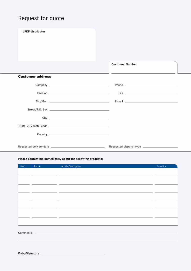
Company
Division
Mr./Mrs.
Street/P.O. Box
City
State, ZIP/postal code
Country
Quantity
Please contact me immediately about the following products:
Item Article DescriptionPart #
Comments
Date/Signature
Phone
Fax
Requested delivery date Requested dispatch type
Customer Number
Customer address
Request for quote
LPKF distributor

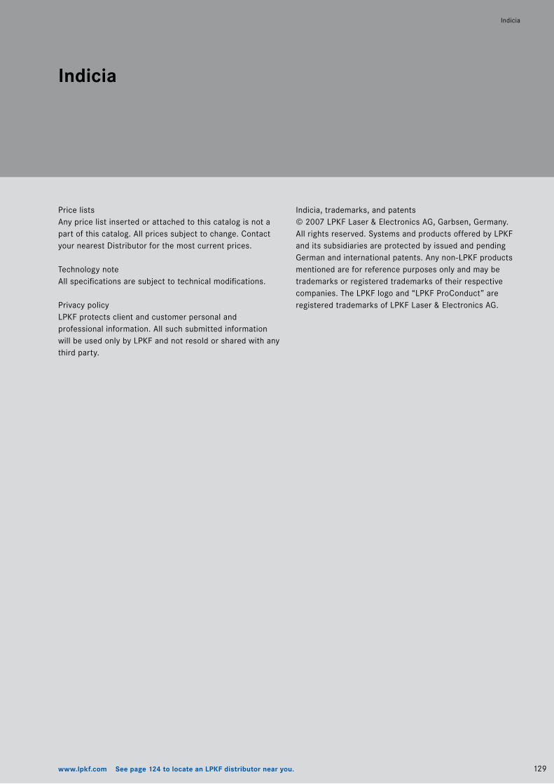
www.lpkf.com See page 124 to locate an LPKF distributor near you.
Price listsAny price list inserted or attached to this catalog is not a part of this catalog. All prices subject to change. Contact your nearest Distributor for the most current prices.
Technology noteAll specifications are subject to technical modifications.
Privacy policyLPKF protects client and customer personal and professional information. All such submitted information will be used only by LPKF and not resold or shared with any third party.
Indicia
Indicia
129
Phone and FaxPhone +49 (0) 5131-7095-0Fax +49 (0) 5131-7095-90
[email protected]@lpkf.de
LPKF websitewww.lpkf.dewww.lpkf.com
LPKF maintains a worldwide distribution network. Find the most convenient one on page 124, or visit www.lpkf.com for more information.
Here you find all information you need. Our competent sales and service team is waiting for your call.
Placing an order? Need technical support? No problem!
Europe (LPKF Headquarters)
North/Central America China
LPKF Sales and Service
Worldwide LPKF distribution partners
Phone and Fax Phone +1 (503) 454-4219Fax +1 (503) 682-7151
[email protected]@lpkfusa.com
LPKF websitewww.lpkfusa.com
Phone and Fax Sales Phone +86-13920308369Service Phone +86-13032289111Fax +86-2223006965
LPKF websitewww.lpkf.cn
Indicia, trademarks, and patents© 2007 LPKF Laser & Electronics AG, Garbsen, Germany. All rights reserved. Systems and products offered by LPKF and its subsidiaries are protected by issued and pending German and international patents. Any non-LPKF products mentioned are for reference purposes only and may be trademarks or registered trademarks of their respective companies. The LPKF logo and “LPKF ProConduct” are registered trademarks of LPKF Laser & Electronics AG.
Process steps
The color-coded steps are only necessary for the production of multilayer boards.
Data preparation
Milling inner layers (2+3 and 4+5)
Bonding multilayer
Marking and drilling
Galvanic through-hole plating
Milling external layers (bonded multilayer)
Cutting out the printed circuit board
Solder resist masks, legend printing
Solder paste printing
Assembling
Reflow soldering
Data preparation
Milling external layers (each layer done before bonding)
Milling inner layers (2+3)
Bonding multilayer
Marking and drilling
Through-hole conductivity without chemicals
Cutting out the printed circuit board
Solder resist masks, legend printing
Solder paste printing
Assembling
Reflow soldering
98
97 & 102
104
106
108
97
106
110
111
112
113
98
97 & 102
97 & 102
104
106
107
106
110
111
112
113
Page
Page
Galvanic through-hole plating
Through-hole plating without chemicals

LPKF-DistributorLPKF Laser & Electronics AGOsteriede 7D-30827 GarbsenGermany
Phone +49(0)5131-7095-0Fax +49(0)5131-7095-90
KF
AG
, 119
838
-10
07-E
N
PRODUCT CATALOG
Circuit Board Plotters
Laser Circuit Structuring
Through-Hole Conductivity
Multilayer Prototyping
SMT/Finishing
Technical Guide
InhouseRapid PCB
Prototyping
www.lpkf.com
PR
OD
UC
T C
ATA
LOG
LPK
F La
ser
& E
lect
roni
cs
Printed circuit board manufacturing – clear and brief
In the workflow overview you will see the simple steps to develop a finished printed circuit board using LPKF technology; process steps for galvanic or chemistry-free through-hole plating are shown. On the declared pages you will find detailed information about the appropriate steps of the production process.
Detailed information starting at page 95.
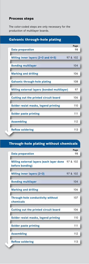