Embed Size (px)
Citation preview
® Liquid Crystal Display Group
LQ035Q7DB02TFT LCD Module
(Model No.: LQ035Q7DB02)
Spec No.: LCY-0204Issue Date: March 14, 2002
TECHNICAL LITERATURE
No. LCY – 02024 DATE MAR. 14. 2002
TECHNICAL LITERATURE
FOR
TFT - LCD module
MODEL No. LQ035Q7DB02
TENTATIVE The technical literature is subject to change without notice. So , please contact Sharp or its representative before designing your product based on this literature.
SHARP CORPORATION
MOBILE LIQUID CRYSTAL DISPLAY GROUP
LCY-02024-1 NOTICE
This publication is the proprietary of SHARP and is copyrighted, with all rights reserved. Under the copyrightlaws, no part of this publication may be reproduced or transmitted in any form or by any means, electronic ormechanical for any purpose, in whole or in part, without the express written permission of SHARP. Expresswritten permission is also required before any use of this publication may be made by a third party.
The application circuit examples in this publication are provided to explain the representative applications ofSHARP's devices and are not intended to guarantee any circuit design or permit any industrial property right orother rights to be executed. SHARP takes no responsibility for any problems related to any industrial propertyright or a third party resulting from the use of SHARP's devices, except for those resulting directly from devicemanufacturing processes.
In the absence of confirmation by device specification sheets, SHARP takes no responsibility for any defects that occur in equipment using any of SHARP's devices, shown in catalogs, data books, etc. Contact SHARP in order toobtain the latest device specification sheets before using any SHARP's device.
SHARP reserves the right to make changes in the specifications, characteristics, data, materials, structures and other contents described herein at any time without notice in order to improve design or reliability. Contact SHARPin order to obtain the latest specification sheets before using any SHARP's device. Manufacturing locations are also subject to change without notice.
Observe the following points when using any device in this publication. SHARP takes no responsibility fordamage caused by improper use of the devices.
The devices in this publication are designed for use in general electronic equipment designs, such as:・Personal computers ・Office automation ・Telecommunication equipment・Test and measurement equipment ・Industrial control・Audio visual and multimedia equipment ・Consumer electronics
The appropriate design measures should be taken to ensure reliability and safety when SHARP's devices are used for equipment such as:・Transportation control and safety equipment(i.e., aircraft, trains, automobiles, etc.)・Traffic signals ・Gas leakage sensor breakers・Alarm equipment ・Various safety devices etc.
SHARP's devices shall not be used for equipment that requires extremely high level of reliability, such as:・Military and space applications ・Nuclear power control equipment・Medical equipment for life support
Contact a SHARP representative, in advance, when intending to use SHARP's devices for any "specific"applications other than those recommended by SHARP.
Contact and consult with a SHARP representative if there are any questions about the contents of thispublication.
sharp
LCY-02024-2 (1) Application This literature applies to LQ035Q7DB02.
(2) OverviewThis module is a color reflective and active matrix LCD module incorporating amorphous silicon TFT
(Thin Film Transistor), named AD-TFT(Advanced TFT). It is composed of a color TFT-LCD panel, driverICs, an FPC, a back light, a touch panel and a back sealed casing. It isn’t composed control circuit.Graphics and texts can be displayed on a 240×3×320 dots panel with 262,144 colors by supplying.
Optimum view angle is 6 o’clock. An inverted display mode is selective in the vertical or the horizontal direction.
(3)Mechanical specifications
Table 1
Parameter Specifications Units Remarks
Screen size (Diagonal) 8.9 [3.52”] Diagonal cm
Display active area 53.64(H)×71.52(V) mm
Pixel format 240(H)×320(V)
(1 pixel = R+G+B dots)pixels
Pixel pitch 0.2235(H)×0.2235(V) mm
Pixel configuration R,G,B vertical stripe
Unit outline dimension 65.0(W)×85.0(H)×4.5 (D) mm 【Note3-1】
Mass 50 g TYP.
Surface hardness 3H【Note 3-1】
Excluding protrusion. For detailed measurements and tolerances, please refer to Fig. 1.
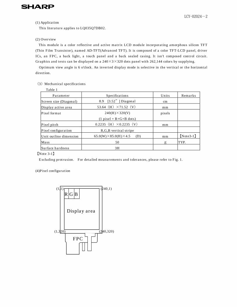
(4)Pixel configuration
R G B
Display area
FPC
(240,1)(1,1)
(240,320)(1,320)
sharp
LCY-02024-3 (5)Input/Output terminal
5-1)TFT-LCD panel driving sectionTable2
Pin No. Symbol I/O Description Remarks
1 VDD - Power supply of gate driver(high level)
2 AGND -
3 MOD I Control signal of gate driver 【Note5-1】
4 MOD I Control signal of gate driver 【Note5-1】
5 U/L I Selection for vertical scanning direction 【Note5-2】
6 SPS I Start signal of gate driver
7 CLS I Clock signal of gate driver
8 AGND -
9 VEE - Power supply of gate driver(low level)
10 VEE - Power supply of gate driver(low level)
11 VCOM I Common electrode driving signal
12 VCOM I Common electrode driving signal
13 SPL I/O Sampling start signal
14 R0 I RED data signal(LSB)
15 R1 I RED data signal
16 R2 I RED data signal
17 R3 I RED data signal
18 R4 I RED data signal
19 R5 I RED data signal(MSB)
20 G0 I GREEN data signal(LSB)
21 G1 I GREEN data signal
22 G2 I GREEN data signal
23 G3 I GREEN data signal
24 G4 I GREEN data signal
25 G5 I GREEN data signal(MSB)
26 B0 I BLUE data signal(LSB)
27 B1 I BLUE data signal
28 B2 I BLUE data signal
29 B3 I BLUE data signal
30 B4 I BLUE data signal
31 B5 I BLUE data signal(MSB)
32 VSHD - Power supply of digital
33 DGND - Ground(digital)
34 PS I Power save signal
35 LP I Data latch signal of source driver
36 DCLK I Data sampling clock signal
37 LBR I Selection for horizontal scanning direction 【Note5-3】
38 SPR I/O Sampling start signal
39 VSHA - Power supply(analog)
sharp
LCY-02024-4
Pin No. Symbol I/O Description Remarks
40 AGND -
41 AGND -
42 REV I reverse control signal
43 COM O Produce REV signal with the amplitude of AGND-VSHA
44 AGND -
45 AGND -
46 AGND -
47 AGND -
48 AGND -
49 AGND -
50 AGND - Ground(Analog)【Note5-1】See section(7-1)-(A) ”※Cautions when you turn on or off the power supply”.【Note5-2】Selection for vertical scanning direction
U/L Scanning direction (Pixel configuration)
Low Normal scanning ( X , 1 ) ↓ ( X , 320 )
High Inverted scanning ( X , 1)↑
( X , 320)
【Note5-3】Selection for horizontal scanning direction
LBR SPL SPR Scanning direction (Pixel configuration)High Input Output Normal scanning (1,Y) → (240,Y)
Low Output Input Inverted scanning (1,Y) ← (240,Y)
5-2)Back light driving sectionTable3
Pin No. Symbol I/O Description Remark
1 VL1 I Power supply for LED (High voltage)2 N.C - -
3 N.C - -
4 VL2 I Power supply for LED (Low voltage)
5 N.C - -
5-3)Touch panel driving sectionTable 4
Pin No. Symbol I/O Description Remark
T1 YU - Lower electrode Y (12 o’clock side)
T2 XR - upper electrode X (right side)
T3 YL - Lower electrode Y (6 o’clock side)
T4 XL - upper electrode X (left side)
sharp
LCY-02024-5 (6)Absolute Maximum Ratings
Table 5
Parameter Symbol Condition Ratings Unit Remark
Power supply(source/Analog) VSHA Ta=25℃ -0.3~+7.0 V
Power supply(source/Digital) VSHD Ta=25℃ -0.3~+7.0 V
Power supply (gate) VDD Ta=25℃ -0.3~+35.0 V
Power supply (gate) VDD-VEE Ta=25℃ -0.3~+35.0 V
Input voltage (Digital) VID Ta=25℃ -0.3~VSHD+0.3 V [Terminal①]
Operating temperature (panel surface)
Topp - 0~50 ℃ 【Note6】
Storage temperature Tstg - -25~70 ℃ 【Note6-2】 [Terminal①] MOD,U/L,SPS,CLS,SPL,R0~R5,G0~G5,B0~B5,LP,DCLK,LBR,SPR,PS,REV【Note6-2】Humidity: 95%RH Max.(at Ta ≦ 40℃). Maximum wet-bulb temperature is less than 39℃(at Ta > 40℃). Condensation of dew must be avoided.
sharp
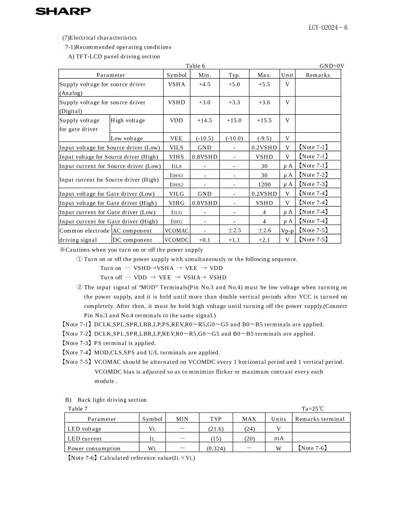
LCY-02024-6 (7)Electrical characteristics
7-1)Recommended operating conditions A) TFT-LCD panel driving section Table 6 GND=0V
Parameter Symbol Min. Typ. Max. Unit RemarksSupply voltage for source driver(Analog)
VSHA +4.5 +5.0 +5.5 V
Supply voltage for source driver(Digital)
VSHD +3.0 +3.3 +3.6 V
Supply voltage for gate driver
High voltage VDD +14.5 +15.0 +15.5 V
Low voltage VEE (-10.5) (-10.0) (-9.5) VInput voltage for Source driver (Low) VILS GND - 0.2VSHD V 【Note 7-1】Input voltage for Source driver (High) VIHS 0.8VSHD - VSHD V 【Note 7-1】Input current for Source driver (Low) IILS - - 30 μA 【Note 7-1】
IIHS1 - - 30 μA 【Note 7-2】Input current for Source driver (High)
IIHS2 - - 1200 μA 【Note 7-3】Input voltage for Gate driver (Low) VILG GND - 0.2VSHD V 【Note 7-4】Input voltage for Gate driver (High) VIHG 0.8VSHD - VSHD V 【Note 7-4】Input current for Gate driver (Low) IILG - - 4 μA 【Note 7-4】Input current for Gate driver (High) IIHG - - 4 μA 【Note 7-4】Common electrode AC component VCOMAC - ±2.5 ±2.6 Vp-p 【Note 7-5】driving signal DC component VCOMDC +0.1 +1.1 +2.1 V 【Note 7-5】
※ Cautions when you turn on or off the power supply ① Turn on or off the power supply with simultaneously or the following sequence.
Turn on … VSHD→VSHA → VEE → VDDTurn off … VDD → VEE → VSHA→ VSHD
② The input signal of “MOD” Terminals(Pin No.3 and No.4) must be low voltage when turning onthe power supply, and it is held until more than double vertical periods after VCC is turned oncompletely. After then, it must be held high voltage until turning off the power supply.(ConnectPin No.3 and No.4 terminals to the same signal.)
【Note 7-1】DCLK,SPL,SPR,LBR,LP,PS,REV,R0~R5,G0~G5 and B0~B5 terminals are applied.【Note 7-2】DCLK,SPL,SPR,LBR,LP,REV,R0~R5,G0~G5 and B0~B5 terminals are applied.【Note 7-3】PS terminal is applied.【Note 7-4】MOD,CLS,SPS and U/L terminals are applied.【Note 7-5】VCOMAC should be alternated on VCOMDC every 1 horizontal period and 1 vertical period.
VCOMDC bias is adjusted so as to minimize flicker or maximum contrast every each module .
B) Back light driving sectionTable 7 Ta=25℃
Parameter Symbol MIN TYP MAX Units Remarks terminal
LED voltage VL - (21.6) (24) VLED current IL - (15) (20) mA
Power consumption WL - (0.324) - W 【Note 7-6】【Note 7-6】Calculated reference value(IL×VL)
sharp
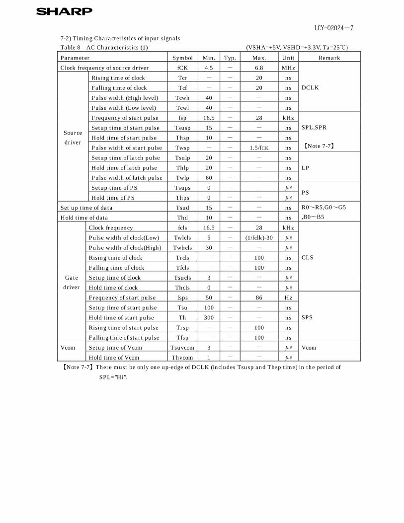
LCY-02024-7 7-2) Timing Characteristics of input signalsTable 8 AC Characteristics (1) (VSHA=+5V, VSHD=+3.3V, Ta=25℃)
Parameter Symbol Min. Typ. Max. Unit Remark
Clock frequency of source driver fCK 4.5 - 6.8 MHz
Rising time of clock Tcr - - 20 ns
Falling time of clock Tcf - - 20 ns
Pulse width (High level) Tcwh 40 - - ns
Pulse width (Low level) Tcwl 40 - - ns
DCLK
Frequency of start pulse fsp 16.5 - 28 kHz
Setup time of start pulse Tsusp 15 - - ns
Hold time of start pulse Thsp 10 - - ns
Pulse width of start pulse Twsp - - 1.5/fCK ns
SPL,SPR
【Note 7-7】
Setup time of latch pulse Tsulp 20 - - ns
Hold time of latch pulse Thlp 20 - - ns LP
Pulse width of latch pulse Twlp 60 - - ns
Setup time of PS Tsups 0 - - μs
Sourcedriver
Hold time of PS Thps 0 - - μsPS
Set up time of data Tsud 15 - - ns
Hold time of data Thd 10 - - ns
R0~R5,G0~G5,B0~B5
Clock frequency fcls 16.5 - 28 kHz
Pulse width of clock(Low) Twlcls 5 - (1/fclk)-30 μs
Pulse width of clock(High) Twhcls 30 - - μs
Rising time of clock Trcls - - 100 ns
Falling time of clock Tfcls - - 100 ns
Setup time of clock Tsucls 3 - - μs
Hold time of clock Thcls 0 - - μs
CLS
Frequency of start pulse fsps 50 - 86 Hz
Setup time of start pulse Tsu 100 - - ns
Hold time of start pulse Th 300 - - ns
Rising time of start pulse Trsp - - 100 ns
Gatedriver
Falling time of start pulse Tfsp - - 100 ns
SPS
Vcom Setup time of Vcom Tsuvcom 3 - - μs Vcom
Hold time of Vcom Thvcom 1 - - μs
【Note 7-7】There must be only one up-edge of DCLK (includes Tsusp and Thsp time) in the period of
SPL=”Hi”.
sharp
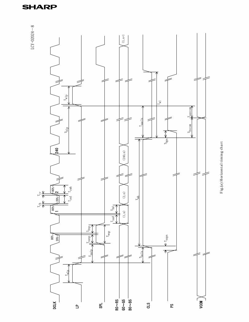
LCY-02024-8
Fig.
(a) H
oriz
onta
l tim
ing
char
t
T wlp
T susp T hsp
(1,n)
(2,n)
(240,n)
(1,n+1
T wlp
T hlp
T sulp
T sud T hd
T cwl T cwh
T ch
T cr �
���
T wsp
T wh
T wl
����
�
�
�����
�� �
�����
��
����
T hcls
T sucls
T sups
T hps
T suvcom
T hvcom
�
sharp
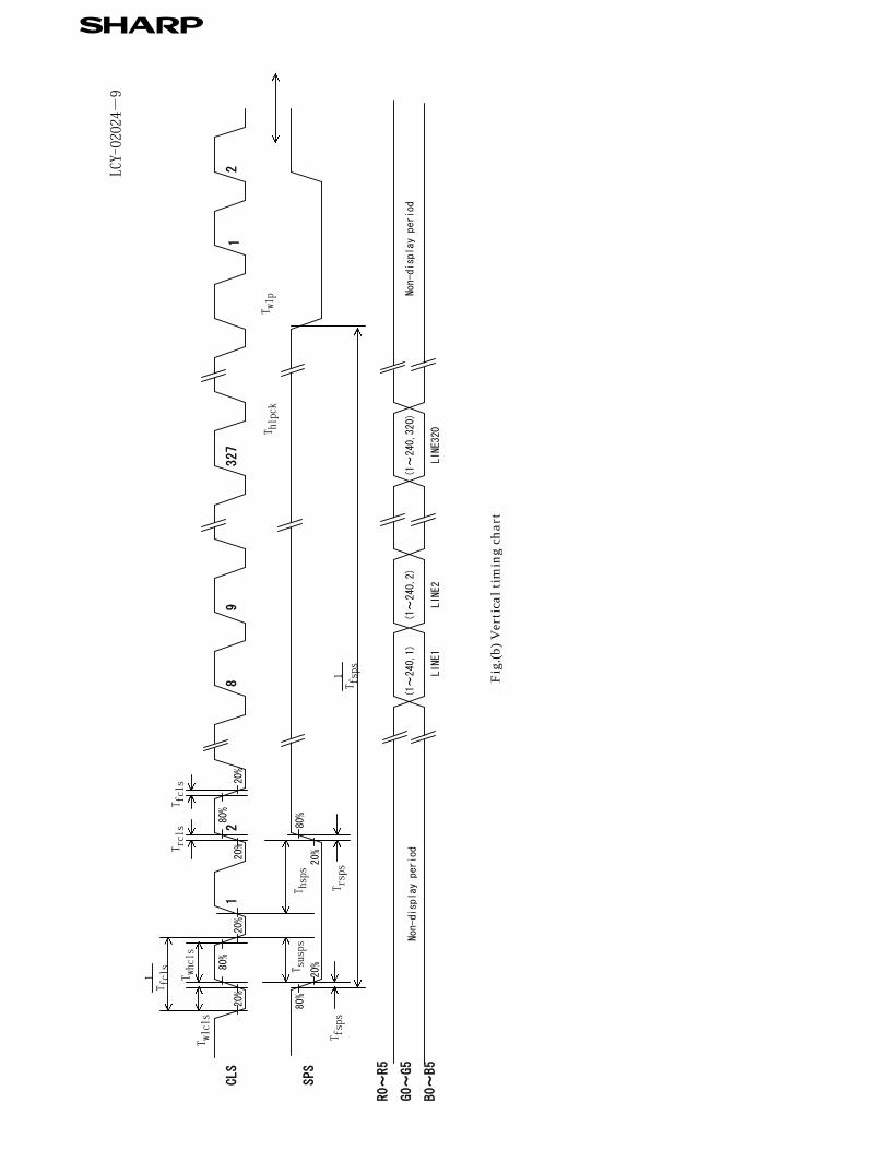
LCY-02024-9
Fig.
(b)V
erti
cal t
imin
g ch
art
�
T susps
T wlp
T hlpck
��
��
����
T hsps
T rcls
T fcls
T rsps
T fsps
��
T fcls 1
T wlcls
T whcls
T fsps 1
�����
�� �
�����
sharp
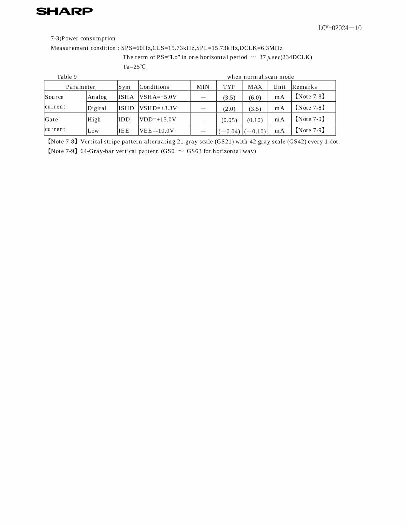
LCY-02024-10 7-3)Power consumptionMeasurement condition : SPS=60Hz,CLS=15.73kHz,SPL=15.73kHz,DCLK=6.3MHz The term of PS=”Lo” in one horizontal period … 37μsec(234DCLK) Ta=25℃
Table 9 when normal scan mode
Parameter Sym Conditions MIN TYP MAX Unit Remarks
Analog ISHA VSHA=+5.0V - (3.5) (6.0) mA 【Note 7-8】Sourcecurrent Digital ISHD VSHD=+3.3V - (2.0) (3.5) mA 【Note 7-8】
High IDD VDD=+15.0V - (0.05) (0.10) mA 【Note 7-9】Gatecurrent Low IEE VEE=-10.0V - (-0.04) (-0.10) mA 【Note 7-9】
【Note 7-8】Vertical stripe pattern alternating 21 gray scale (GS21) with 42 gray scale (GS42) every 1 dot.【Note 7-9】64-Gray-bar vertical pattern (GS0 ~ GS63 for horizontal way)
sharp
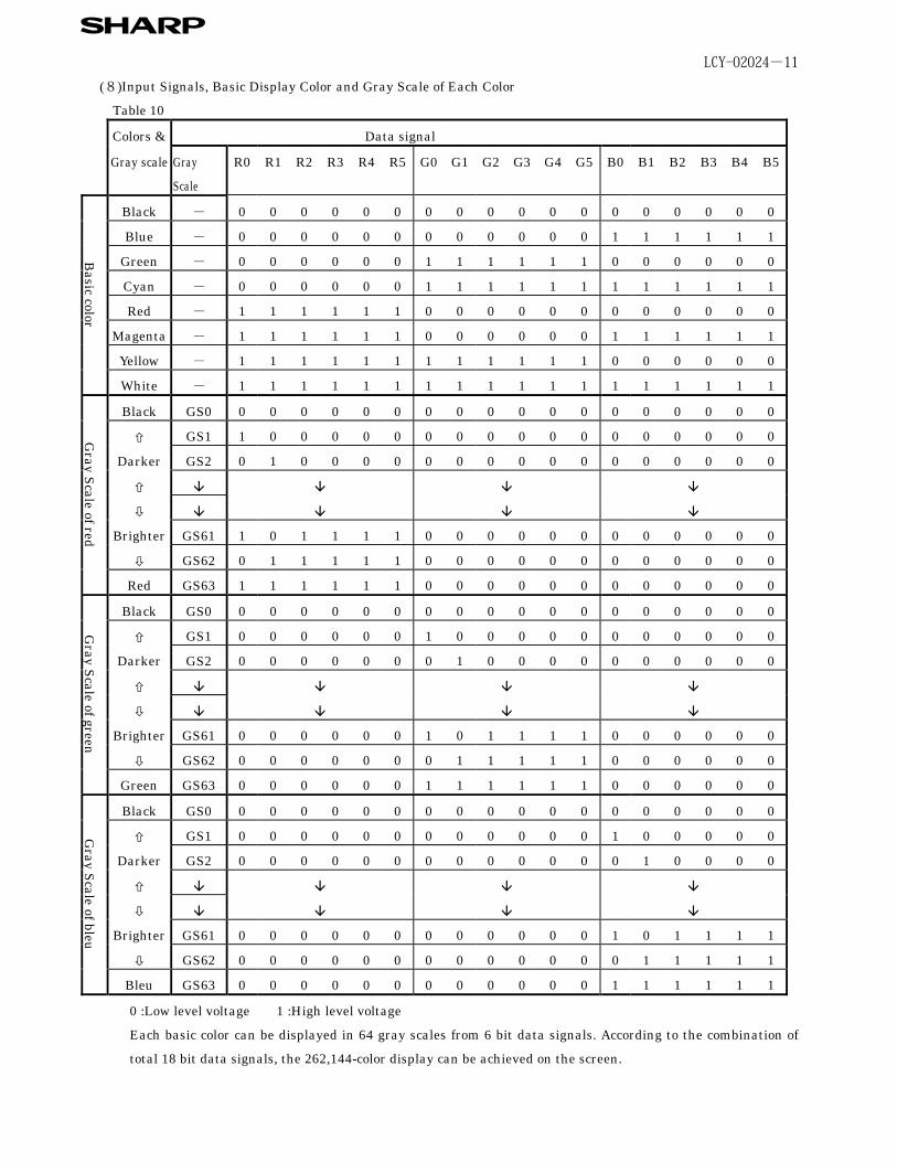
LCY-02024-11 (8)Input Signals, Basic Display Color and Gray Scale of Each Color
Table 10
Colors & Data signal
Gray scale Gray
Scale
R0 R1 R2 R3 R4 R5 G0 G1 G2 G3 G4 G5 B0 B1 B2 B3 B4 B5
Black - 0 0 0 0 0 0 0 0 0 0 0 0 0 0 0 0 0 0
Blue - 0 0 0 0 0 0 0 0 0 0 0 0 1 1 1 1 1 1
Green - 0 0 0 0 0 0 1 1 1 1 1 1 0 0 0 0 0 0
Cyan - 0 0 0 0 0 0 1 1 1 1 1 1 1 1 1 1 1 1
Red - 1 1 1 1 1 1 0 0 0 0 0 0 0 0 0 0 0 0
Magenta - 1 1 1 1 1 1 0 0 0 0 0 0 1 1 1 1 1 1
Yellow - 1 1 1 1 1 1 1 1 1 1 1 1 0 0 0 0 0 0
Basic color
White - 1 1 1 1 1 1 1 1 1 1 1 1 1 1 1 1 1 1
Black GS0 0 0 0 0 0 0 0 0 0 0 0 0 0 0 0 0 0 0
GS1 1 0 0 0 0 0 0 0 0 0 0 0 0 0 0 0 0 0
Darker GS2 0 1 0 0 0 0 0 0 0 0 0 0 0 0 0 0 0 0
Brighter GS61 1 0 1 1 1 1 0 0 0 0 0 0 0 0 0 0 0 0
GS62 0 1 1 1 1 1 0 0 0 0 0 0 0 0 0 0 0 0
Gray Scale of red
Red GS63 1 1 1 1 1 1 0 0 0 0 0 0 0 0 0 0 0 0
Black GS0 0 0 0 0 0 0 0 0 0 0 0 0 0 0 0 0 0 0
GS1 0 0 0 0 0 0 1 0 0 0 0 0 0 0 0 0 0 0
Darker GS2 0 0 0 0 0 0 0 1 0 0 0 0 0 0 0 0 0 0
Brighter GS61 0 0 0 0 0 0 1 0 1 1 1 1 0 0 0 0 0 0
GS62 0 0 0 0 0 0 0 1 1 1 1 1 0 0 0 0 0 0
Gray Scale of green
Green GS63 0 0 0 0 0 0 1 1 1 1 1 1 0 0 0 0 0 0
Black GS0 0 0 0 0 0 0 0 0 0 0 0 0 0 0 0 0 0 0
GS1 0 0 0 0 0 0 0 0 0 0 0 0 1 0 0 0 0 0
Darker GS2 0 0 0 0 0 0 0 0 0 0 0 0 0 1 0 0 0 0
Brighter GS61 0 0 0 0 0 0 0 0 0 0 0 0 1 0 1 1 1 1
GS62 0 0 0 0 0 0 0 0 0 0 0 0 0 1 1 1 1 1
Gray Scale of bleu
Bleu GS63 0 0 0 0 0 0 0 0 0 0 0 0 1 1 1 1 1 1
0 :Low level voltage 1 :High level voltage
Each basic color can be displayed in 64 gray scales from 6 bit data signals. According to the combination of
total 18 bit data signals, the 262,144-color display can be achieved on the screen.
sharp
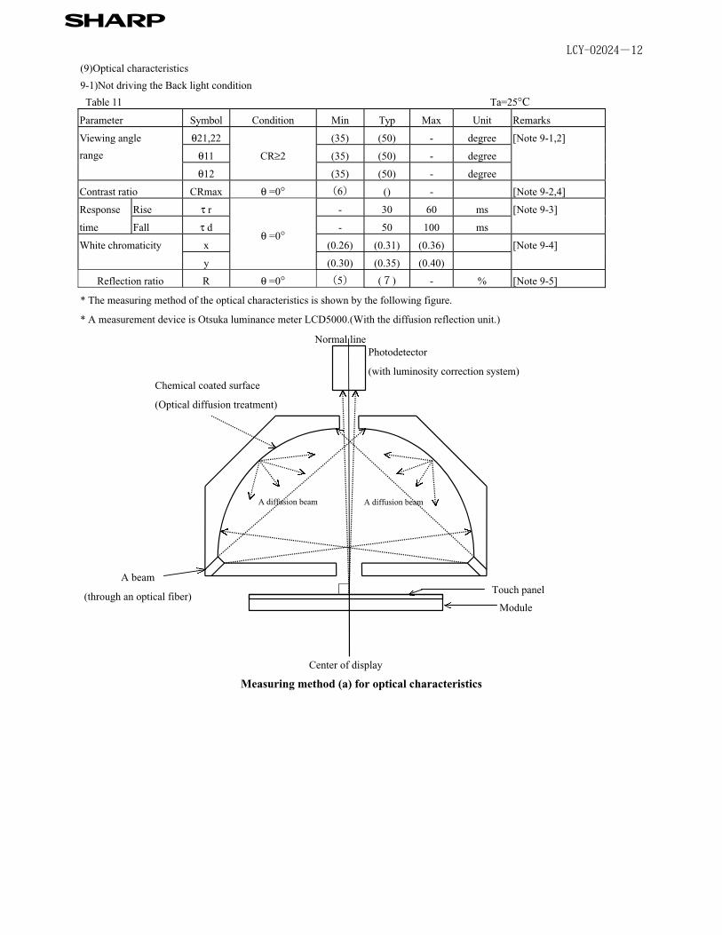
LCY-02024-12 (9)Optical characteristics
9-1)Not driving the Back light condition
Table 11 Ta=25°C
Parameter Symbol Condition Min Typ Max Unit Remarks
θ21,22 (35) (50) - degree [Note 9-1,2]
θ11 CR≥2 (35) (50) - degree
Viewing angle
range
θ12 (35) (50) - degree
Contrast ratio CRmax θ =0° (6) () - [Note 9-2,4]
Response Rise τ r - 30 60 ms [Note 9-3]
time Fall τ d - 50 100 ms
White chromaticity x (0.26) (0.31) (0.36) [Note 9-4]
y
θ =0°
(0.30) (0.35) (0.40)
Reflection ratio R θ =0° (5) (7) - % [Note 9-5]
* The measuring method of the optical characteristics is shown by the following figure.
* A measurement device is Otsuka luminance meter LCD5000.(With the diffusion reflection unit.)
Center of display
Measuring method (a) for optical characteristics
Photodetector
(with luminosity correction system)
Module
Chemical coated surface
(Optical diffusion treatment)
A diffusion beam A diffusion beam
Normal line
A beam
(through an optical fiber)Touch panel
sharp
LCY-02024-13
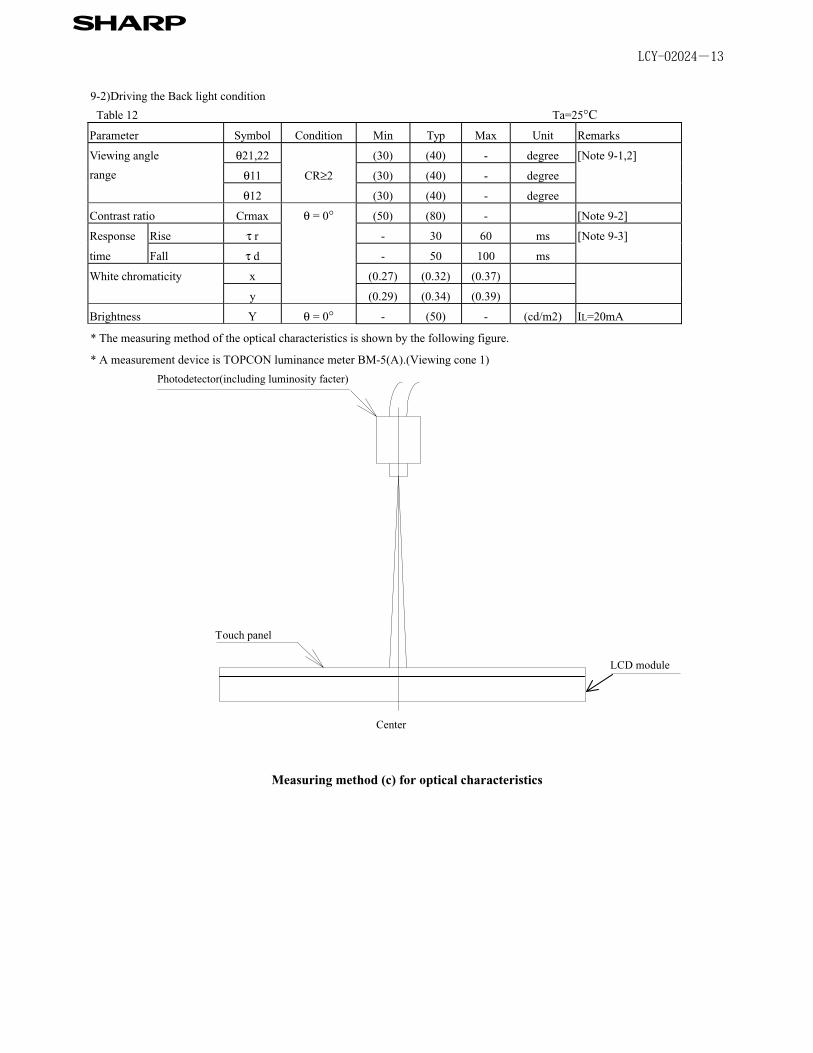
9-2)Driving the Back light condition
Table 12 Ta=25°C
Parameter Symbol Condition Min Typ Max Unit Remarks
θ21,22 (30) (40) - degree [Note 9-1,2]
θ11 CR≥2 (30) (40) - degree
Viewing angle
range
θ12 (30) (40) - degree
Contrast ratio Crmax θ = 0° (50) (80) - [Note 9-2]
Response Rise τ r - 30 60 ms [Note 9-3]
time Fall τ d - 50 100 ms
White chromaticity x (0.27) (0.32) (0.37)
y (0.29) (0.34) (0.39)
Brightness Y θ = 0° - (50) - (cd/m2) IL=20mA
* The measuring method of the optical characteristics is shown by the following figure.
* A measurement device is TOPCON luminance meter BM-5(A).(Viewing cone 1)
Measuring method (c) for optical characteristics
Photodetector(including luminosity facter)
Center
Touch panel
LCD module
sharp
LCY-02024-14
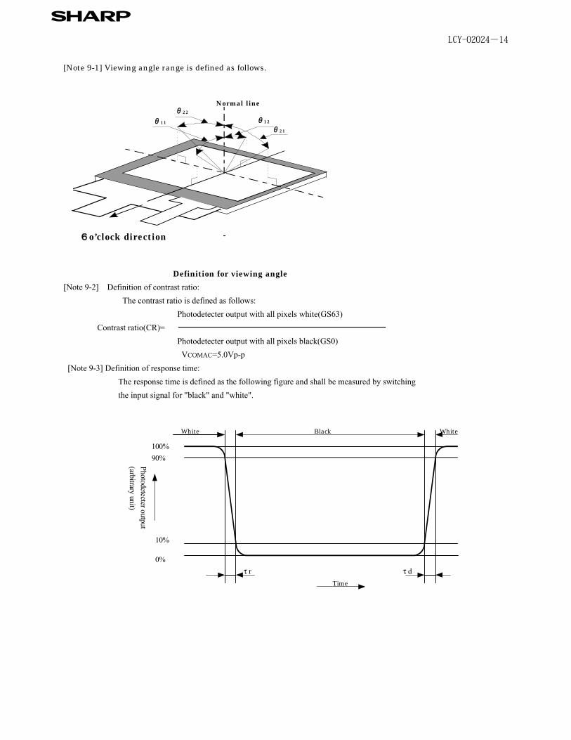
[Note 9-1] Viewing angle range is defined as follows.
�o’clock direction
�1 2
�2 2
�1 1
�2 1
Normal line
Definition for viewing angle [Note 9-2] Definition of contrast ratio:
The contrast ratio is defined as follows:
Photodetecter output with all pixels white(GS63)
Contrast ratio(CR)=
Photodetecter output with all pixels black(GS0)
VCOMAC=5.0Vp-p
[Note 9-3] Definition of response time:
The response time is defined as the following figure and shall be measured by switching
the input signal for "black" and "white".
0%
10%
90%
100%
Black WhiteWhite
τ dτ r
Time
Photodetecter output
(arbitrary unit)
sharp
LCY-02024-15 [Note 9-4] A measurement device is Minolta CM-2002.
[Note 9-5] Definition of reflection ratio
Reflection ratio =
(10)Touch panel characteristicsTable 13
Parameter Min. Typ. Max. Unit RemarkInput voltage - 5.0 7.0 VResistor between terminals(X1-X2) 300 480 900 Ω
Resistor between terminals(Y1-Y2) 200 419 850 ΩProvisionalspecification
Accuracy of detecting dimension - - ±1.0 %Line linearity(X direction) - - 1.5 %Line linearity(Y direction) - - 1.5 %Insuration resistance 20 - - MΩ at DC25VMinimum tension for detecting 0.1 - 0.79 N
(11)Display quality The display quality of the color TFT-LCD module shall be in compliance with
the Incoming Inspection Standards for TFT-LCD..
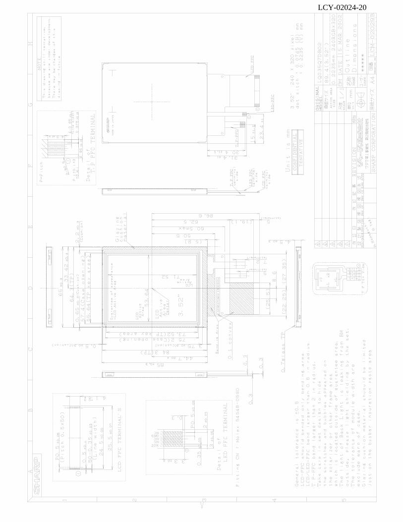
(12)Mechanical characteristics 12-1) External appearance See Fig. 1 12-2) FPC (for LCD panel) characteristics
(1)Specific connector FH12A-50S-0.5SH(HIROSE)
(2) Bending endurance of the bending slits portion No line of the FPC is broken for the bending test (Bending radius=0.6mm and angle=90°) in 30 cycles.
12-3) Design guidance for touchpanel(T/P) 12-3-1)Example of housing design (1)If an consumer will put a palm on housing in normal usage, care should be taken as follows.
(2)Keep the gap, for example 0.3 to 0.7mm,between bezel edge and T/P surface.The reason is to avoid the bezel edge from contacting T/P surface that may cause a “short”with bottom layer(See Fig.2)
(3)Insertion a cushion material is recommended. (4)The cushion material should be limited just on the busbar insulation paste area. If it is over the transparent insulation paste area, a ”short” may be occurred. (5)There is one where a resistance film is left in the T/P part of the end of the pole. Design to keep insulation from the perimeter to prevent from mis-operation and so on.
Light detected level of the reflection by the LCD module
Light detected level of the reflection by the standard white board
sharp
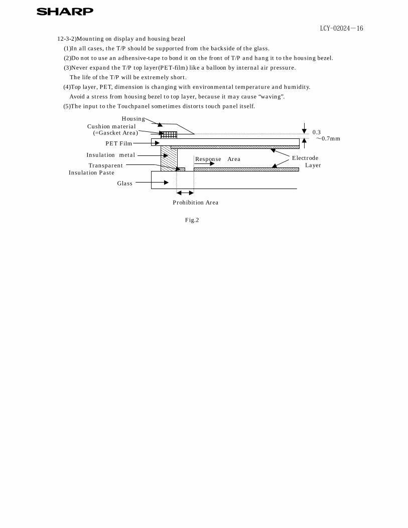
LCY-02024-16 12-3-2)Mounting on display and housing bezel
(1)In all cases, the T/P should be supported from the backside of the glass.(2)Do not to use an adhensive-tape to bond it on the front of T/P and hang it to the housing bezel.(3)Never expand the T/P top layer(PET-film) like a balloon by internal air pressure.
The life of the T/P will be extremely short. (4)Top layer, PET, dimension is changing with environmental temperature and humidity. Avoid a stress from housing bezel to top layer, because it may cause “waving”.
(5)The input to the Touchpanel sometimes distorts touch panel itself.
Fig.2
HousingCushion material
PET Film
Insulation metal
Glass
TransparentInsulation Paste
Response Area
Prohibition Area
ElectrodeLayer
0.3~0.7mm
(=Gascket Area)
sharp
LCY-02024-17 (13)Handling Precautions 13-1) Insertion and taking out of FPCs Be sure insert and take out of the FPC into the connector of the set after turning off the power supply on the set side. 13-2) Handling of FPCs
The FPC for LCD panel shall be bent only slit portion. The bending slit shall be bent uniformly on the whole slit portion with bending radius larger than 0.6mm ,and only inner side (back sideof the module). Don’t bend it outer side (display surface side).
Don’t give the FPCs too large force, for example, hanging the module with holding FPC. 12-3) Installation of the module
On mounting the module, be sure to fix the module on the same plane. Taking care not to warp or twist the module.
13-4)Precaution when mounting(1) If water droplets and oil attaches to it for a long time, discoloration and staining occurs. Wipe them off
immediately.(2) Glass is used for the TFT-LCD panel. If it is dropped or bumped against a hard object, it may be broken.
Handle it with sufficient care.(3)As the CMOS IC is used in this module, pay attention to static electricity when handling it. Take ameasure for grounding on the human body.
13-5)Others(1) The liquid-crystal is deteriorated by ultraviolet rays. Do not leave it in direct sunlight and strong
ultraviolet rays for many hours.(2) If it is kept at a temperature below the rated storage temperature, it becomes coagulated and the panel
may be broken. Also, if it is kept at a temperature above the rated storage temperature, it becomesisotropic liquid and does not return to its original state. Therefore, it is desirable to keep it at roomtemperature as much as possible.
(3) If the LCD breaks, don’t put internal liquid crystal into the mouth. When the liquid crystal sticks to the hands, feet and clothes, wash it out immediately.
(4) Wipe off water drop or finger grease immediately. Long contact with water may cause discoloration orspots.
(5) Observe general precautions for all electronic components.(6) VCOM must be adjusted on condition of your final product. No adjustment causes the deterioration for
display quality.(7) Static image should not be displayed more than 5 minutes in order to prevent from occurrence of
residual image.
sharp
LCY-02024-18
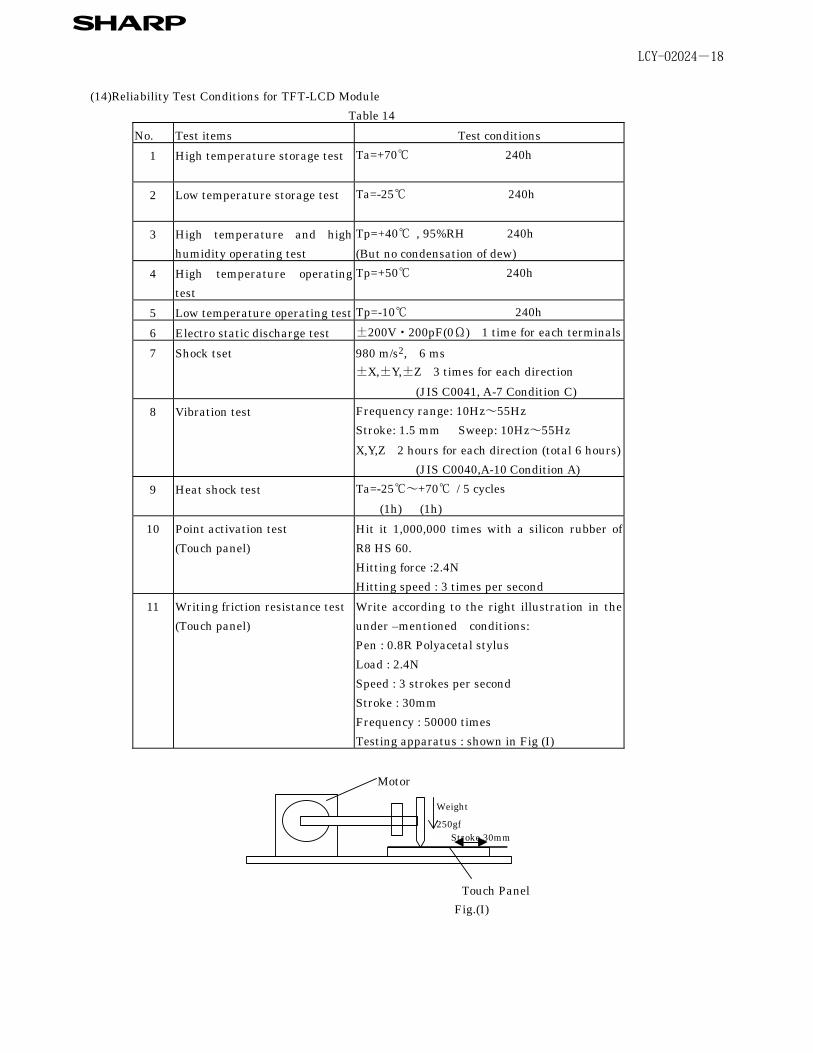
(14)Reliability Test Conditions for TFT-LCD Module Table 14
No. Test items Test conditions
1 High temperature storage test Ta=+70℃ 240h
2 Low temperature storage test Ta=-25℃ 240h
3 High temperature and highhumidity operating test
Tp=+40℃ , 95%RH 240h
(But no condensation of dew)
4 High temperature operatingtest
Tp=+50℃ 240h
5 Low temperature operating test Tp=-10℃ 240h
6 Electro static discharge test ±200V・200pF(0Ω) 1 time for each terminals
7 Shock tset 980 m/s2, 6 ms±X,±Y,±Z 3 times for each direction
(JIS C0041, A-7 Condition C)
8 Vibration test Frequency range: 10Hz~55HzStroke: 1.5 mm Sweep: 10Hz~55Hz
X,Y,Z 2 hours for each direction (total 6 hours) (JIS C0040,A-10 Condition A)
9 Heat shock test Ta=-25℃~+70℃ / 5 cycles
(1h) (1h)
10 Point activation test(Touch panel)
Hit it 1,000,000 times with a silicon rubber ofR8 HS 60. Hitting force :2.4N Hitting speed : 3 times per second
11 Writing friction resistance test(Touch panel)
Write according to the right illustration in theunder –mentioned conditions:Pen : 0.8R Polyacetal stylusLoad : 2.4N Speed : 3 strokes per second Stroke : 30mmFrequency : 50000 times Testing apparatus : shown in Fig (I)
Motor
Touch Panel
Stroke 30mm
Weight
250gf
Fig.(I)
sharp
LCY-02024-19 【Note】Ta = Ambient temperature, Tp = Panel temperature【Check items】
(a)Test No.1~9
In the standard condition, there shall be no practical problems that may affect the display function.(b)Test No.10~No.11
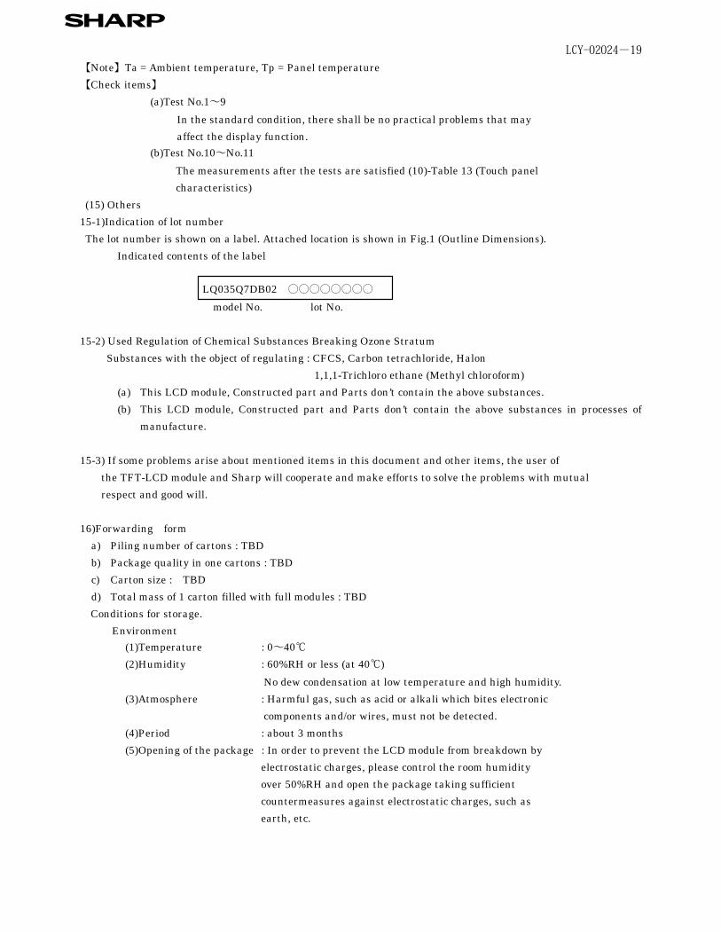
The measurements after the tests are satisfied (10)-Table 13 (Touch panel characteristics) (15) Others15-1)Indication of lot number The lot number is shown on a label. Attached location is shown in Fig.1 (Outline Dimensions). Indicated contents of the label
LQ035Q7DB02 ○○○○○○○○ model No. lot No.
15-2) Used Regulation of Chemical Substances Breaking Ozone Stratum Substances with the object of regulating : CFCS, Carbon tetrachloride, Halon 1,1,1-Trichloro ethane (Methyl chloroform)
(a) This LCD module, Constructed part and Parts don’t contain the above substances. (b) This LCD module, Constructed part and Parts don’t contain the above substances in processes of
manufacture. 15-3) If some problems arise about mentioned items in this document and other items, the user of the TFT-LCD module and Sharp will cooperate and make efforts to solve the problems with mutual respect and good will.
16)Forwarding forma) Piling number of cartons : TBDb) Package quality in one cartons : TBDc) Carton size : TBDd) Total mass of 1 carton filled with full modules : TBDConditions for storage.
Environment(1)Temperature : 0~40℃(2)Humidity : 60%RH or less (at 40℃)
No dew condensation at low temperature and high humidity.(3)Atmosphere : Harmful gas, such as acid or alkali which bites electronic components and/or wires, must not be detected.(4)Period : about 3 months(5)Opening of the package : In order to prevent the LCD module from breakdown by
electrostatic charges, please control the room humidity over 50%RH and open the package taking sufficient
countermeasures against electrostatic charges, such as earth, etc.
sharp
LCY-02024-20
SPECIFICATIONS ARE SUBJECT TO CHANGE WITHOUT NOTICE.Suggested applications (if any) are for standard use; See Important Restrictions for limitations on special applications. See Limited �Warranty for SHARP’s product warranty. The Limited Warranty is in lieu, and exclusive of, all other warranties, express or implied. �ALL EXPRESS AND IMPLIED WARRANTIES, INCLUDING THE WARRANTIES OF MERCHANTABILITY, FITNESS FOR USE AND �FITNESS FOR A PARTICULAR PURPOSE, ARE SPECIFICALLY EXCLUDED. In no event will SHARP be liable, or in any way responsible,�for any incidental or consequential economic or property damage.
NORTH AMERICA EUROPE JAPAN
SHARP Microelectronics of the Americas5700 NW Pacific Rim Blvd.Camas, WA 98607, U.S.A.Phone: (1) 360-834-2500Fax: (1) 360-834-8903Fast Info: (1) 800-833-9437www.sharpsma.com
SHARP Microelectronics EuropeDivision of Sharp Electronics (Europe) GmbHSonninstrasse 320097 Hamburg, GermanyPhone: (49) 40-2376-2286Fax: (49) 40-2376-2232www.sharpsme.com
SHARP CorporationElectronic Components & Devices22-22 Nagaike-cho, Abeno-KuOsaka 545-8522, JapanPhone: (81) 6-6621-1221Fax: (81) 6117-725300/6117-725301www.sharp-world.com
TAIWAN SINGAPORE KOREA
SHARP Electronic Components(Taiwan) Corporation8F-A, No. 16, Sec. 4, Nanking E. Rd.Taipei, Taiwan, Republic of ChinaPhone: (886) 2-2577-7341Fax: (886) 2-2577-7326/2-2577-7328
SHARP Electronics (Singapore) PTE., Ltd.438A, Alexandra Road, #05-01/02Alexandra Technopark, Singapore 119967Phone: (65) 271-3566Fax: (65) 271-3855
SHARP Electronic Components(Korea) CorporationRM 501 Geosung B/D, 541Dohwa-dong, Mapo-kuSeoul 121-701, KoreaPhone: (82) 2-711-5813 ~ 8Fax: (82) 2-711-5819
CHINA HONG KONG
SHARP Microelectronics of China(Shanghai) Co., Ltd.28 Xin Jin Qiao Road King Tower 16FPudong Shanghai, 201206 P.R. ChinaPhone: (86) 21-5854-7710/21-5834-6056Fax: (86) 21-5854-4340/21-5834-6057Head Office:No. 360, Bashen Road, Xin Development Bldg. 22Waigaoqiao Free Trade Zone Shanghai200131 P.R. ChinaEmail: [email protected]
SHARP-ROXY (Hong Kong) Ltd.3rd Business Division,17/F, Admiralty Centre, Tower 118 Harcourt Road, Hong KongPhone: (852) 28229311Fax: (852) 28660779www.sharp.com.hkShenzhen Representative Office:Room 13B1, Tower C,Electronics Science & Technology BuildingShen Nan Zhong RoadShenzhen, P.R. ChinaPhone: (86) 755-3273731Fax: (86) 755-3273735