Embed Size (px)
Citation preview
LT1683
11683fd
TYPICAL APPLICATION
DESCRIPTION
Slew Rate Controlled Ultralow Noise Push-Pull DC/DC Controller
The LT®1683 is a switching regulator controller designed to lower conducted and radiated electromagnetic interference (EMI). Ultralow noise and EMI are achieved by controlling the voltage and current slew rates of external N-channel MOSFET switches. Current and voltage slew rates can be independently set to optimize harmonic content of the switching waveforms vs efficiency. The LT1683 can reduce high frequency harmonic power by as much as 40dB with only minor losses in efficiency. The LT1683 utilizes a dual output (push-pull) current mode architecture optimized for low noise topologies. The IC includes gate drivers and all necessary oscillator, control and protection circuitry. Unique error amp circuitry can regulate both positive and negative voltages. The oscil-lator may be synchronized to an external clock for more accurate placement of switching harmonics.
Protection features include gate drive lockout for low VIN, opposite gate lockout, soft-start, output current limit, short-circuit current limiting, gate drive overvoltage clamp and input supply undervoltage lockout.
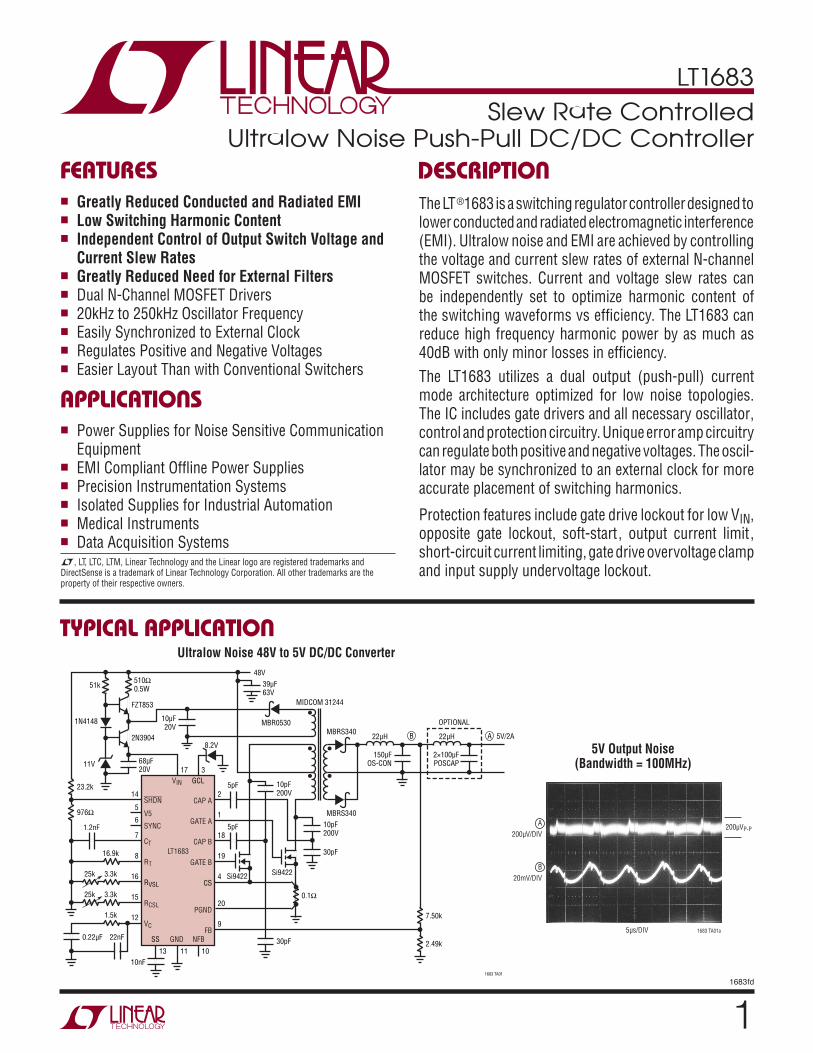
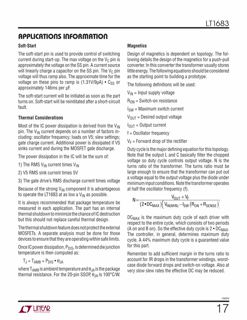
Ultralow Noise 48V to 5V DC/DC Converter
FEATURES
APPLICATIONS
n Greatly Reduced Conducted and Radiated EMIn Low Switching Harmonic Contentn Independent Control of Output Switch Voltage and
Current Slew Ratesn Greatly Reduced Need for External Filtersn Dual N-Channel MOSFET Driversn 20kHz to 250kHz Oscillator Frequencyn Easily Synchronized to External Clockn Regulates Positive and Negative Voltagesn Easier Layout Than with Conventional Switchers
n Power Supplies for Noise Sensitive Communication Equipment
n EMI Compliant Offline Power Suppliesn Precision Instrumentation Systemsn Isolated Supplies for Industrial Automationn Medical Instrumentsn Data Acquisition Systems
ABMBRS340
MIDCOM 31244
22µH
150µFOS-CON
MBRS340
MBR0530
22µH
OPTIONAL
2×100µFPOSCAP
5V/2A
3
10
1683 TA01
1113
SHDN CAP A
NFB
LT1683
GND
VIN
17
14 2
GCL
SS
V5
SYNCGATE A
51
CT CAP B
6
18
RT GATE B
7
198
RCSL
16
VC
15
12
RVSL CS4
PGND20
FB9
5pF
5pF
Si9422Si9422
0.1Ω
976Ω
23.2k
10nF
1.5k
3.3k
25k
25k
3.3k
16.9k
1.2nF
39µF63V
48V
68µF20V
11V
8.2V
51k510Ω0.5W
2N3904
1N4148 10µF20V
30pF22nF0.22µF
7.50k
2.49k
FZT853
10pF200V
30pF
10pF200V
5V Output Noise(Bandwidth = 100MHz)
A200µV/DIV
B20mV/DIV
200µVP-P
5µs/DIV 1683 TA01a
L, LT, LTC, LTM, Linear Technology and the Linear logo are registered trademarks and DirectSense is a trademark of Linear Technology Corporation. All other trademarks are the property of their respective owners.
LT1683
21683fd
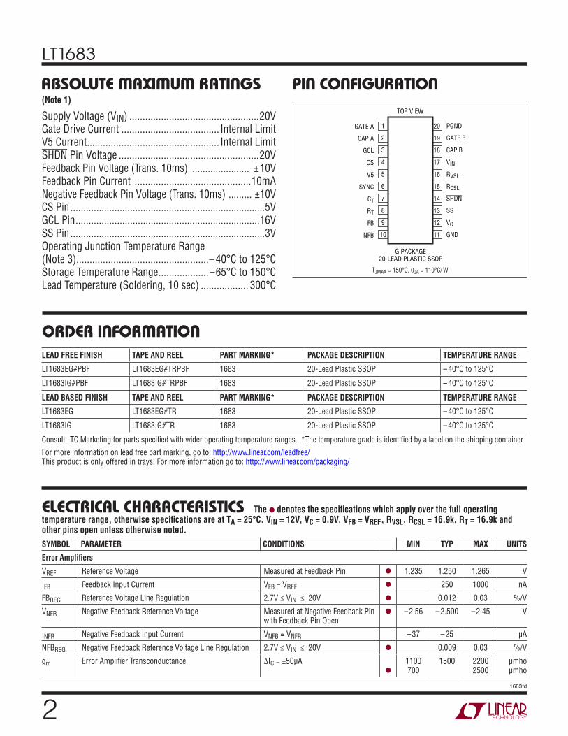
PIN CONFIGURATIONABSOLUTE MAXIMUM RATINGS
Supply Voltage (VIN) .................................................20VGate Drive Current ..................................... Internal LimitV5 Current .................................................. Internal LimitSHDN Pin Voltage .....................................................20VFeedback Pin Voltage (Trans. 10ms) ...................... ±10VFeedback Pin Current ............................................10mANegative Feedback Pin Voltage (Trans. 10ms) ......... ±10VCS Pin ...........................................................................5VGCL Pin .......................................................................16VSS Pin ...........................................................................3VOperating Junction Temperature Range(Note 3) ..................................................–40°C to 125°CStorage Temperature Range ...................–65°C to 150°CLead Temperature (Soldering, 10 sec) .................. 300°C
(Note 1)
1
2
3
4
5
6
7
8
9
10
TOP VIEW
G PACKAGE20-LEAD PLASTIC SSOP
20
19
18
17
16
15
14
13
12
11
GATE A
CAP A
GCL
CS
V5
SYNC
CT
RT
FB
NFB
PGND
GATE B
CAP B
VIN
RVSL
RCSL
SHDN
SS
VC
GND
TJMAX = 150°C, θJA = 110°C/ W
ELECTRICAL CHARACTERISTICS
SYMBOL PARAMETER CONDITIONS MIN TYP MAX UNITS
Error Amplifiers
VREF Reference Voltage Measured at Feedback Pin l 1.235 1.250 1.265 V
IFB Feedback Input Current VFB = VREF l 250 1000 nA
FBREG Reference Voltage Line Regulation 2.7V ≤ VIN ≤ 20V l 0.012 0.03 %/V
VNFR Negative Feedback Reference Voltage Measured at Negative Feedback Pin with Feedback Pin Open
l –2.56 –2.500 –2.45 V
INFR Negative Feedback Input Current VNFB = VNFR –37 –25 µA
NFBREG Negative Feedback Reference Voltage Line Regulation 2.7V ≤ VIN ≤ 20V l 0.009 0.03 %/V
gm Error Amplifier Transconductance ∆IC = ±50µA
l
1100 700
1500 2200 2500
µmho µmho
The denotes the specifications which apply over the full operating temperature range, otherwise specifications are at TA = 25°C. VIN = 12V, VC = 0.9V, VFB = VREF, RVSL, RCSL = 16.9k, RT = 16.9k and other pins open unless otherwise noted.
ORDER INFORMATIONLEAD FREE FINISH TAPE AND REEL PART MARKING* PACKAGE DESCRIPTION TEMPERATURE RANGE
LT1683EG#PBF LT1683EG#TRPBF 1683 20-Lead Plastic SSOP –40°C to 125°C
LT1683IG#PBF LT1683IG#TRPBF 1683 20-Lead Plastic SSOP –40°C to 125°C
LEAD BASED FINISH TAPE AND REEL PART MARKING* PACKAGE DESCRIPTION TEMPERATURE RANGE
LT1683EG LT1683EG#TR 1683 20-Lead Plastic SSOP –40°C to 125°C
LT1683IG LT1683IG#TR 1683 20-Lead Plastic SSOP –40°C to 125°C
Consult LTC Marketing for parts specified with wider operating temperature ranges. *The temperature grade is identified by a label on the shipping container.For more information on lead free part marking, go to: http://www.linear.com/leadfree/ This product is only offered in trays. For more information go to: http://www.linear.com/packaging/
LT1683
31683fd
SYMBOL PARAMETER CONDITIONS MIN TYP MAX UNITS
IESK Error Amp Sink Current VFB = VREF + 150mV, VC = 0.9V l 120 200 350 µA
IESRC Error Amp Source Current VFB = VREF – 150mV, VC = 0.9V l 120 200 350 µA
VCLH Error Amp Clamp Voltage High Clamp, VFB = 1V 1.27 V
VCLL Error Amp Clamp Voltage Low Clamp, VFB = 1.5V 0.12 V
AV Error Amplifier Voltage Gain 180 250 V/V
FBOV FB Overvoltage Shutdown Outputs Drivers Disabled 1.47 V
ISS Soft-Start Charge Current VSS = 1V 9.0 12 µA
Oscillator and Sync
fMAX Max Switch Frequency 250 kHz
fSYNC Synchronization Frequency Range Oscillator Frequency = 250kHz 290 kHz
VSYNC SYNC Pin Input Threshold l 0.7 1.4 2.0
RSYNC SYNC Pin Input Resistance 40 kΩ
Gate Drives (Specifications Apply to Either A or B Unless Otherwise Noted)
DCMAX Maximum Switch Duty Cycle RVSL = RCSL = 4.85k, Osc Frequency = 25kHz
l 45 46 %
VGON Gate On Voltage VIN = 12, GCL = 12 VIN = 12, GCL = 8
10 7.6
10.4 7.9
10.7 8.1
V V
VGOFF Gate Off Voltage VIN = 12V 0.2 0.35 V
IGSO Max Gate Source Current VIN = 12V 0.3 A
IGSK Max Gate Sink Current VIN = 12V 0.3 A
VINUVLO Gate Drive Undervoltage Lockout (Note 5) VGCL = 6.5V, Gates Enabled 7.3 7.5 V
Current Sense
tIBL Switch Current Limit Blanking Time 100 ns
VSENSE Sense Voltage Shutdown Voltage VC Pulled Low l 86 103 120 mV
VSENSEF Sense Voltage Fault Threshold l 230 300 mV
Slew Control (for the Following Slew Tests See Test Circuit in Figure 1b)
VSLEWR Output Voltage Slew Rising Edge RVSL = RCSL = 17k 26 V/µs
VSLEWF Output Voltage Slew Falling Edge RVSL = RCSL = 17k 19 V/µs
VISLEWR Output Current Slew Rising Edge (CS Pin Voltage) RVSL = RCSL = 17k 0.21 V/µs
VISLEWF Output Current Slew Falling Edge (CS Pin Voltage) RVSL = RCSL = 17k 0.21 V/µs
Supply and Protection
VINMIN Minimum Input Voltage (Note 4) VGCL = VIN l 2.55 3.6 V
IVIN Supply Current (Note 2) RVSL = RCSL = 17k , VIN = 12 RVSL = RCSL = 17k , VIN = 20
l
l
25 35
45 55
mA mA
VSHDN Shutdown Turn-On Threshold l 1.31 1.39 1.48 V
∆VSHDN Shutdown Turn-On Voltage Hysteresis l 50 110 180 mV
ISHDN Shutdown Input Current Hysteresis l 10 24 35 µA
V5 5V Reference Voltage 6.5V ≤ VIN ≤ 20V, IV5 = 5mA 6.5V ≤ VIN ≤ 20V, IV5 = –5mA
4.85 4.80
5 5
5.20 5.15
V V
IV5SC 5V Reference Short-Circuit Current VIN = 6.5V Source VIN = 6.5V Sink
10 –10
mA mA
ELECTRICAL CHARACTERISTICS The denotes the specifications which apply over the full operating temperature range, otherwise specifications are at TA = 25°C. VIN = 12V, VC = 0.9V, VFB = VREF, RVSL, RCSL = 16.9k, RT = 16.9k and other pins open unless otherwise noted.
LT1683
41683fd
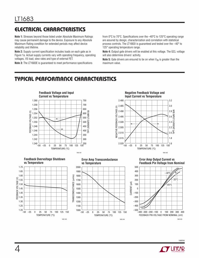
Feedback Voltage and Input Current vs Temperature
Negative Feedback Voltage and Input Current vs Temperature
Feedback Overvoltage Shutdown vs Temperature
Error Amp Transconductance vs Temperature
Error Amp Output Current vs Feedback Pin Voltage from Nominal
ELECTRICAL CHARACTERISTICSNote 1: Stresses beyond those listed under Absolute Maximum Ratings may cause permanent damage to the device. Exposure to any Absolute Maximum Rating condition for extended periods may affect device reliability and lifetime.Note 2: Supply current specification includes loads on each gate as in Figure 1a. Actual supply currents vary with operating frequency, operating voltages, V5 load, slew rates and type of external FET.Note 3: The LT1683E is guaranteed to meet performance specifications
from 0°C to 70°C. Specifications over the –40°C to 125°C operating range are assured by design, characterization and correlation with statistical process controls. The LT1683I is guaranteed and tested over the –40° to 125° operating temperature range.Note 4: Output gate drivers will be enabled at this voltage. The GCL voltage will also determine drivers’ activity.Note 5: Gate drivers are ensured to be on when VIN is greater than the maximum value.
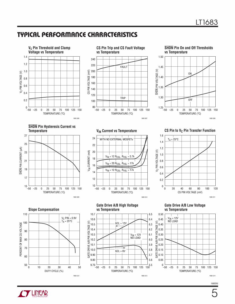
TYPICAL PERFORMANCE CHARACTERISTICS
TEMPERATURE (°C)–50 –25 0 25 50 75 100 125 150
FEED
BACK
VOL
TAGE
(V)
1683 G01
1.260
1.258
1.256
1.254
1.252
1.250
1.248
1.246
1.244
1.242
1.240
FB INPUT CURRENT (nA)
750
700
650
600
550
500
450
400
350
300
250
TEMPERATURE (°C)–50 –25 0 25 50 75 100 125 150
NEGA
TIVE
FEE
DBAC
K VO
LTAG
E (V
)
1683 G02
2.480
2.485
2.490
2.495
2.500
2.505
2.510
2.515
2.520
NFB INPUT CURRENT (µA)
3.2
3.0
2.8
2.6
2.4
2.2
2.0
1.8
1.6
TEMPERATURE (°C)–50 –25 0 25 50 75 100 125 150
FEED
BACK
VOL
TAGE
(V)
1683 G03
1.70
1.65
1.60
1.55
1.50
1.45
1.40
1.35
1.30
1.25
1.20
TEMPERATURE (°C)–50 –25 0 25 50 75 100 125 150
TRAN
SCON
DUCT
ANCE
(µm
ho)
1683 G04
2000
1900
1800
1700
1600
1500
1400
1300
1200
1100
1000
FEEDBACK PIN VOLTAGE FROM NOMINAL (mV)–400 –300 –200 –100 0 100 200 300 400
CURR
ENT
(µA)
1683 G05
500
400
300
200
100
0
–100
–200
–300
–400
–500
–40°C
125°C
25°C
LT1683
51683fd
TYPICAL PERFORMANCE CHARACTERISTICS
VIN Current vs Temperature CS Pin to VC Pin Transfer Function
Slope CompensationGate Drive A/B High Voltage vs Temperature
Gate Drive A/B Low Voltage vs Temperature
CS Pin Trip and CS Fault Voltage vs Temperature
SHDN Pin On and Off Thresholds vs Temperature
SHDN Pin Hysteresis Current vs Temperature
VC Pin Threshold and Clamp Voltage vs Temperature
TEMPERATURE (°C)–50 –25 0 25 50 75 100 125 150
V C P
IN V
OLTA
GE (V
)
1683 G06
1.4
1.2
1.0
0.8
0.6
0.4
0.2
0
TEMPERATURE (°C)–50 –25 0 25 50 75 100 125 150
CS P
IN V
OLTA
GE (m
V)
1683 G07
240
220
200
180
160
140
120
100
80
FAULT
TRIP
TEMPERATURE (°C)–50 –25 0 25 50 75 100 125 150
SHDN
PIN
VOL
TAGE
(V)
1683 G08
1.50
1.45
1.40
1.35
1.30
1.25
ON
OFF
TEMPERATURE (°C)–50 –25 0 25 50 75 100 125 150
SHDN
PIN
CUR
RENT
(µA)
1683 G09
27
25
23
21
19
17
15
TEMPERATURE (°C)–50 –25 0 25 50 75 100 125 150
V IN
CURR
ENT
(mA)
1683 G10
24
22
20
18
16
14
12
10
VIN = 12 RCSL, RVSL = 5.7k
WITH NO EXTERNAL MOSFETs
VIN = 20 RCSL, RVSL = 17k
VIN = 12 RCSL, RVSL = 17k
CS PIN VOLTAGE (mV)0 20 40 60 80 100 120
V C P
IN V
OLTA
GE (V
)
1683 G11
1.6
1.4
1.2
1.0
0.8
0.6
0.4
0.2
0
TA = 25°C
DUTY CYCLE (%)0 10 20 30 40 50
PERC
ENT
OF M
AX C
S VO
LTAG
E
1683 G12
110
100
90
80
70
60
50
VC PIN = 0.9VTA = 25°C
TEMPERATURE (°C)–50 –25 0 25 50 75 100 125 150
GATE
DRI
VE A
/B P
IN V
OLTA
GE (V
)
1683 G13
10.7
10.6
10.5
10.4
10.3
10.2
10.1
10.0
9.90
9.80
9.70
6.5
6.4
6.3
6.2
6.1
6.0
5.9
5.8
5.7
5.6
5.5
GCL = 12V
GCL = 6V
VIN = 12VNO LOAD
TEMPERATURE (°C)–50 –25 0 25 50 75 100 125 150
GATE
DRI
VE A
/B P
IN V
OLTA
GE (V
)
1683 G14
0.50
0.45
0.40
0.35
0.30
0.25
0.20
0.15
0.10
0.05
0
VIN = 12VNO LOAD
LT1683
61683fd
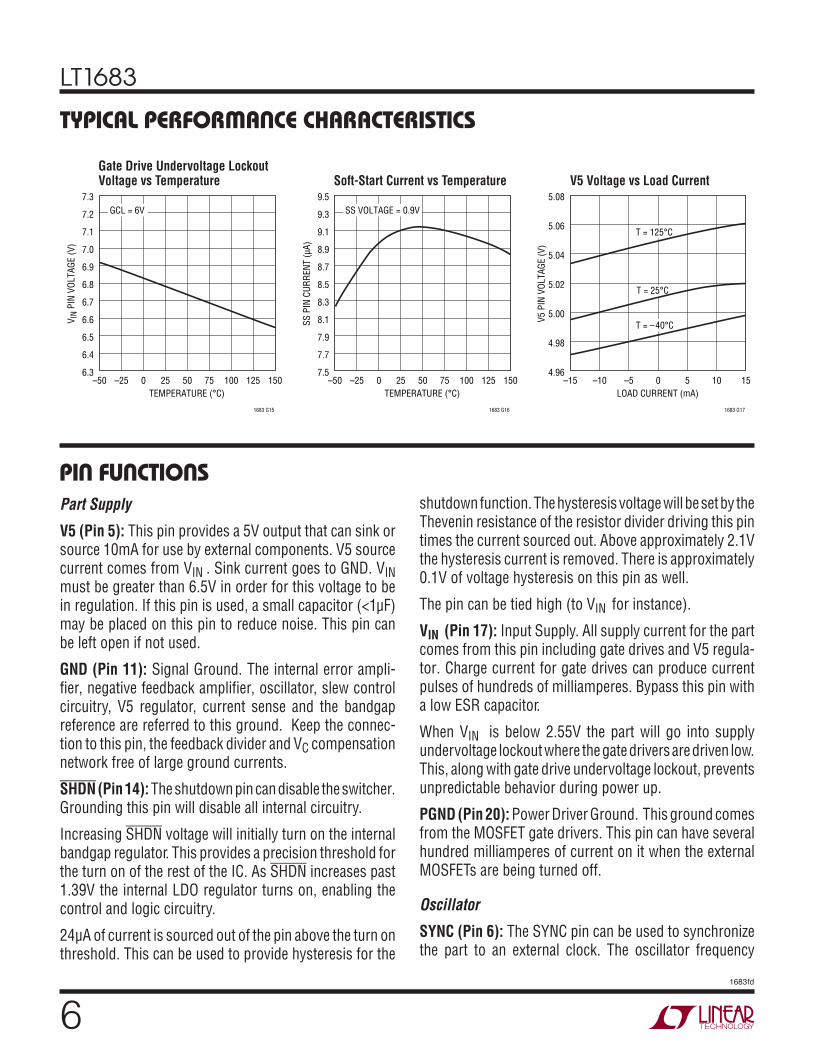
TYPICAL PERFORMANCE CHARACTERISTICS
Soft-Start Current vs Temperature V5 Voltage vs Load Current Gate Drive Undervoltage Lockout Voltage vs Temperature
TEMPERATURE (°C)–50 –25 0 25 50 75 100 125 150
V IN
PIN
VOLT
AGE
(V)
1683 G15
7.3
7.2
7.1
7.0
6.9
6.8
6.7
6.6
6.5
6.4
6.3
GCL = 6V
TEMPERATURE (°C)–50 –25 0 25 50 75 100 125 150
SS P
IN C
URRE
NT (µ
A)
1683 G16
9.5
9.3
9.1
8.9
8.7
8.5
8.3
8.1
7.9
7.7
7.5
SS VOLTAGE = 0.9V
LOAD CURRENT (mA)–15 –10 –5 0 5 10 15
V5 P
IN V
OLTA
GE (V
)
1683 G17
5.08
5.06
5.04
5.02
5.00
4.98
4.96
T = 125°C
T = 25°C
T = –40°C
PIN FUNCTIONSPart Supply
V5 (Pin 5): This pin provides a 5V output that can sink or source 10mA for use by external components. V5 source current comes from VIN . Sink current goes to GND. VIN must be greater than 6.5V in order for this voltage to be in regulation. If this pin is used, a small capacitor (<1µF) may be placed on this pin to reduce noise. This pin can be left open if not used.
GND (Pin 11): Signal Ground. The internal error ampli-fier, negative feedback amplifier, oscillator, slew control circuitry, V5 regulator, current sense and the bandgap reference are referred to this ground. Keep the connec-tion to this pin, the feedback divider and VC compensation network free of large ground currents.
SHDN (Pin 14): The shutdown pin can disable the switcher. Grounding this pin will disable all internal circuitry.
Increasing SHDN voltage will initially turn on the internal bandgap regulator. This provides a precision threshold for the turn on of the rest of the IC. As SHDN increases past 1.39V the internal LDO regulator turns on, enabling the control and logic circuitry.
24µA of current is sourced out of the pin above the turn on threshold. This can be used to provide hysteresis for the
shutdown function. The hysteresis voltage will be set by the Thevenin resistance of the resistor divider driving this pin times the current sourced out. Above approximately 2.1V the hysteresis current is removed. There is approximately 0.1V of voltage hysteresis on this pin as well.
The pin can be tied high (to VIN for instance).
VIN (Pin 17): Input Supply. All supply current for the part comes from this pin including gate drives and V5 regula-tor. Charge current for gate drives can produce current pulses of hundreds of milliamperes. Bypass this pin with a low ESR capacitor.
When VIN is below 2.55V the part will go into supply undervoltage lockout where the gate drivers are driven low. This, along with gate drive undervoltage lockout, prevents unpredictable behavior during power up.
PGND (Pin 20): Power Driver Ground. This ground comes from the MOSFET gate drivers. This pin can have several hundred milliamperes of current on it when the external MOSFETs are being turned off.
Oscillator
SYNC (Pin 6): The SYNC pin can be used to synchronize the part to an external clock. The oscillator frequency
LT1683
71683fd
PIN FUNCTIONS should be set close to the external clock frequency. Syn-chronizing the clock to an external reference is useful for creating more stable positioning of the switcher voltage and current harmonics. This pin can be left open or tied to ground if not used.
CT (Pin 7): The oscillator capacitor pin is used in conjunc-tion with RT to set the oscillator frequency. For RT = 16.9k:
COSC(nf) = 129/fOSC(kHz)
RT (Pin 8): The oscillator resistor pin is used to set the charge and discharge currents of the oscillator capacitor. The nominal value is 16.9k. It is possible to adjust this re-sistance ±25% to set oscillator frequency more accurately.
Gate Drive
GATE A, GATE B (Pins 1, 19): These pins connect to the gates of the external N-channel MOSFETs. GATE A and GATE B turn on with alternate clock cycles. These drivers are capable of sinking and sourcing at least 300mA.
The GCL pin sets the upper voltage of the gate drive. The gate pins will not be activated until VIN reaches a minimum voltage as defined by the GCL pin (gate undervoltage lockout).
The gate drive outputs have current limit protection to safe guard against accidental shorts.
If the gate drive voltage is greater than about 1V the opposite gate drive is inhibited thus preventing cross conduction.
GCL (Pin 3): This pin sets the maximum gate voltage to the GATE A and GATE B pins to the MOSFET gate drives. This pin should be either tied to a Zener, a voltage source or VIN.
If the pin is tied to a Zener or a voltage source, the maximum gate drive voltage will be approximately VGCL – 0.2V. If it is tied to VIN, the maximum gate voltage is approximately VIN – 1.6.
Approximately 50µA of current can be sourced from this pin if VGCL < VIN – 0.8V.
This pin also controls undervoltage lockout of the gate drives. If the pin is tied to a Zener or voltage source, the
gate drive will not be enabled until VIN > VGCL + 0.8V. If this pin is tied to VIN, then undervoltage lockout is disabled.
There is an internal 19V Zener tied from this pin to ground to provide a fail-safe for maximum gate voltage.
Slew Control
CAP A, CAP B (Pins 2, 18): These pins are the feedback nodes for the external voltage slewing capacitors. Normally a small 1pf to 5pf capacitor is connected from this pin to the drain of its respective MOSFET.
The voltage slew rate is inversely proportional to this capacitance and proportional to the current that the part will sink and source on this pin. That current is inversely proportional to RVSL.
RCSL (Pin 15): A resistor to ground sets the current slew rate for the external drive MOSFETs during switching. The minimum resistor value is 3.3k and the maximum value is 68k. The time to slew between on and off states of the MOSFET current will determine how the di/dt related harmonics are reduced. This time is proportional to RCSL and RS (the current sense resistor) and maximum cur-rent. Longer times produce a greater reduction of higher frequency harmonics.
RVSL (Pin 16): A resistor to ground sets the voltage slew rate for the drains of the external drive MOSFETs. The minimum resistor value is 3.3k and the maximum value is 68k. The time to slew between on and off states on the MOSFET drain voltage will determine how harmonics are reduced from this source. This time is proportional to RVSL, CVA/B and the input voltage. Longer times produce more rolloff of harmonics. CVA/B is the equivalent capacitance from CAP A or B to the drain of the MOSFET.
Switch Mode Control
CS (Pin 4): This is the input to the current sense amplifier. It is used for both current mode control and current slewing of the external MOSFETs. Current sense is accomplished via a sense resistor (RS) connected from the sources of the external MOSFETs to ground. CS is connected to the top of RS. Current sense is referenced to the GND pin.
LT1683
81683fd
PIN FUNCTIONSThe switch maximum operating current will be equal to 0.1V/RS. At CS = 0.1V, the gate drivers will be immediately turned off (no slew control).
If CS = 0.22V in addition to the drivers being turned off, VC and SS will be discharged to ground (short-circuit protec-tion). This will hasten turn off on subsequent cycles.
FB (Pin 9): The feedback pin is used for positive voltage sensing. It is the inverting input to the error amplifier. The noninverting input of this amplifier connects internally to a 1.25V reference.
If the voltage on this pin exceeds the reference by 220mV, then the output drivers will immediately turn off the exter-nal MOSFETs (no slew control). This provides for output overvoltage protection
When this input is below 0.9V then the current sense blanking will be disabled. This will assist start up.
NFB (Pin 10): The negative feedback pin is used for sens-ing a negative output voltage. The pin is connected to the inverting input of the negative feedback amplifier through a 100k source resistor. The negative feedback amplifier provides a gain of –0.5 to the FB pin. The nominal regula-tion point would be –2.5V on NFB. This pin should be left open if not used.
If NFB is being used then overvoltage protection will occur at 0.44V below the NFB regulation point.
At NFB < –1.8 current sense blanking will be disabled.
VC (Pin 12): The compensation pin is used for frequency compensation and current limiting. It is the output of the error amplifier and the input of the current comparator. Loop frequency compensation can be performed with an RC network connected from the VC pin to ground. The voltage on VC is proportional to the switch peak current. The normal range of voltage on this pin is 0.25V to 1.27V. However, during slope compensation the upper clamp voltage is allowed to increase with the compensation.
During a short-circuit fault the VC pin will be discharged to ground.
SS (Pin 13): The SS pin allows for ramping of the switch current threshold at startup. Normally a capacitor is placed on this pin to ground. An internal 9µA current source will charge this capacitor up. The voltage on the VC pin cannot exceed the voltage on SS. Thus peak current will ramp up as the SS pin ramps up. During a short circuit fault the SS pin will be discharged to ground thus reinitializing soft-start.
When SS is below the VC clamp voltage the VC pin will closely track the SS pin.
This pin can be left open if not used.
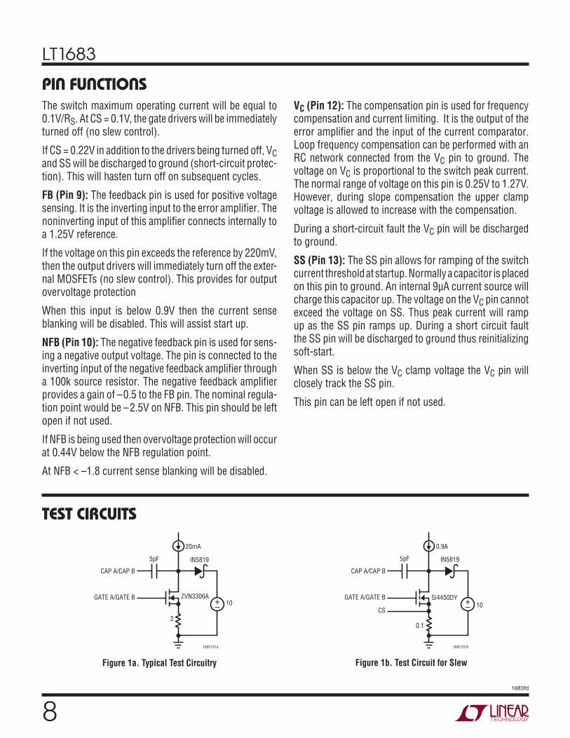
TEST CIRCUITS
+–
5pF IN5819
20mA
2
1683 F01a
ZVN3306A10
GATE A/GATE B
CAP A/CAP B
Figure 1a. Typical Test Circuitry Figure 1b. Test Circuit for Slew
+–
5pF IN5819
0.9A
0.1
1683 F01b
Si4450DY10
GATE A/GATE B
CS
CAP A/CAP B
LT1683
91683fd
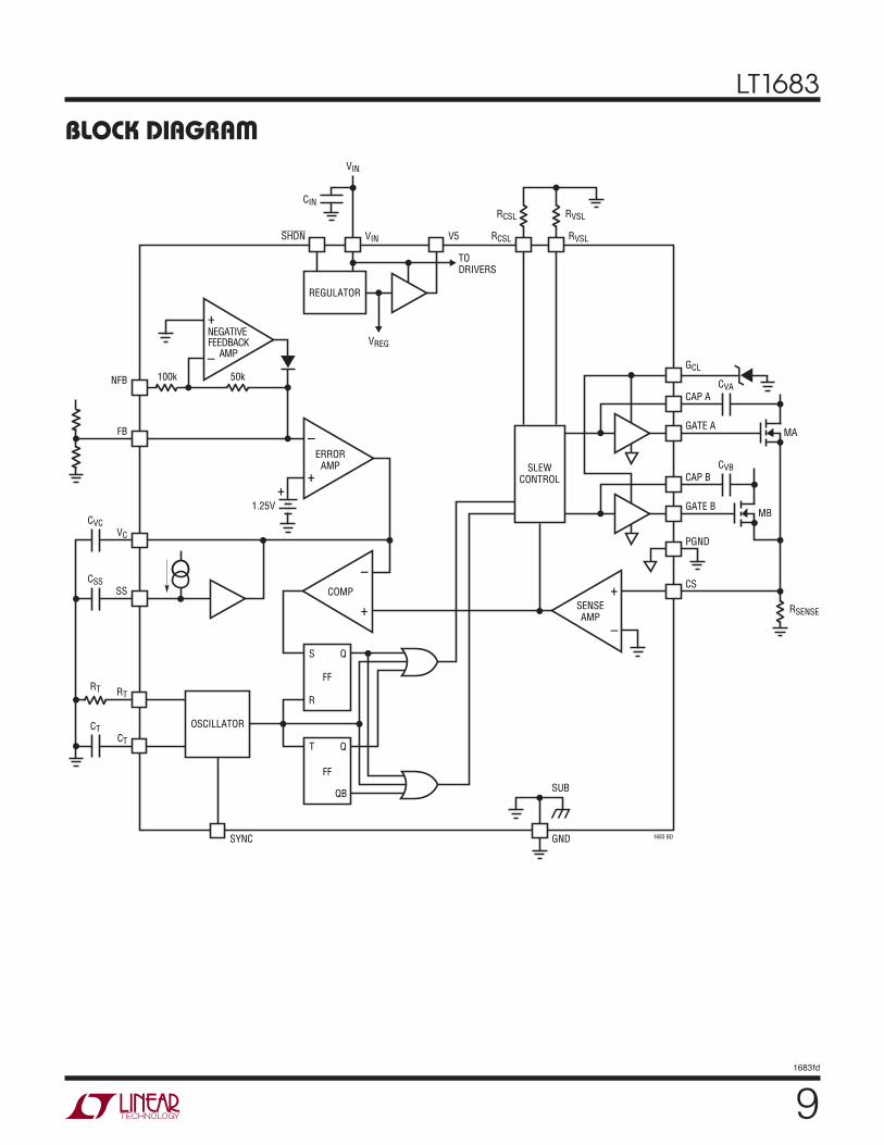
BLOCK DIAGRAM
+
VC
NFB
FB
1683 BD
SSCSS
SLEWCONTROL
VREG
VIN
VIN
CIN
V5
TO DRIVERS
T
QB
Q
FF
S Q
FF
R
OSCILLATOR
–
+NEGATIVE FEEDBACK
AMP
+
–
–
+
ERRORAMP
1.25V
100k 50k
COMP
–
+SENSEAMP
SHDN RVSLRCSL
RCSL
REGULATOR
CVC
RT
CT
CT
RT
RVSL
CAP A
CAP B
GATE AMA
GCL
GATE B
PGND
CS
MB
CVA
CVB
RSENSE
SYNC GND
SUB
LT1683
101683fd
OPERATIONIn noise sensitive applications switching regulators tend to be ruled out as a power supply option due to their pro-pensity for generating unwanted noise. When switching supplies are required due to efficiency or input/output constraints, great pains must be taken to work around the noise generated by a typical supply. These steps may include pre and post regulator filtering, precise synchroni-zation of the power supply oscillator to an external clock, synchronizing the rest of the circuit to the power supply oscillator or halting power supply switching during noise sensitive operations. The LT1683 greatly simplifies the task of eliminating supply noise by enabling the design of an inherently low noise switching regulator power supply.
The LT1683 is a fixed frequency, current mode switching regulator with unique circuitry to control the voltage and current slew rates of the output switches. Current mode control provides excellent AC and DC line regulation and simplifies loop compensation.
Slew control capability provides much greater control over the power supply components that can create conducted and radiated electromagnetic interference. Compliance with EMI standards will be an easier task and will require fewer external filtering components.
The LT1683 uses two external N-channel MOSFETs as the power switches. This allows the user to tailor the drive conditions to a wide range of voltages and currents.
CURRENT MODE CONTROL
Referring to the Block Diagram. A switching cycle begins with an oscillator discharge pulse, which resets the RS flip-flop, turning on one of the external MOSFET drivers. The switch current is sensed across the external sense resistor and the resulting voltage is amplified and com-pared to the output of the error amplifier (VC pin). The driver is turned off once the output of the current sense amplifier exceeds the voltage on the VC pin. In this way pulse by pulse current limit is achieved. The toggle flip-flop ensures that the two MOSFETs are enabled on alternate clock cycles. Internal slope compensation is provided to ensure stability under high duty cycle conditions.
Output regulation is obtained using the error amp to set the switch current trip point. The error amp is a transconductance amplifier that integrates the difference between the feedback output voltage and an internal 1.25V reference. The output of the error amp adjusts the switch current trip point to provide the required load current at the desired regulated output voltage. This method of controlling current rather than voltage provides faster input transient response, cycle-by-cycle current limiting for better output switch protection and greater ease in compensating the feedback loop. The VC pin is used for loop compensation and current limit adjustment. During normal operation the VC voltage will be between 0.25V and 1.27V. An external clamp on VC or SS may be used for lowering the current limit.
The negative voltage feedback amplifier allows for direct regulation of negative output voltages. The voltage on the NFB pin gets amplified by a gain of – 0.5 and driven on to the FB input, i.e., the NFB pin regulates to –2.5V while the amplifier output internally drives the FB pin to 1.25V as in normal operation. The negative feedback amplifier input impedance is 100k (typ) referred to ground.
Soft-Start
Control of the switch current during start-up can be obtained by using the SS pin. An external capacitor from SS to ground is charged by an internal 9µA current source. The voltage on VC cannot exceed the voltage on SS. Thus as the SS pin ramps up the VC voltage will be allowed to ramp up. This will then provide for a smooth increase in switch maximum current. SS will be discharged as a result of the CS voltage exceeding the short-circuit threshold of approximately 0.22V.
Slew Control
Control of output voltage and current slew rates is achieved via two feedback loops. One loop controls the MOSFET drain dV/dt and the other loop controls the MOSFET dI/dt.
The voltage slew rate uses an external capacitor between CAP A or CAP B and the respective MOSFET drain. These integrating caps close the voltage feedback loop. The external resistor, RVSL, sets the current for the integrator.
LT1683
111683fd
The voltage slew rate is thus inversely proportional to both the value of capacitor and RVSL.
The current slew feedback loop consists of the voltage across the external sense resistor, which is internally ampli-fied and differentiated. The derivative is limited to a value set by RCSL. The current slew rate is thus inversely proportional to both the value of sense resistor and RCSL.
The two control loops are combined internally so that a smooth transition from current slew control to voltage slew control is obtained. When turning on, the driver cur-rent will slew before voltage. When turning off, voltage will slew before current. In general it is desirable to have RVSL and RCSL of similar value.
Internal Regulator
Most of the control circuitry operates from an internal 2.4V low dropout regulator that is powered from VIN. The internal low dropout design allows VIN to vary from 2.7V to 20V with stable operation of the controller. When SHDN < 1.3V the internal regulator is completely disabled.
5V Regulator
A 5V regulator is provided for powering external circuitry. This regulator draws current from VIN and requires VIN to be greater than 6.5V to be in regulation. It can sink or source 10mA. The output is current limited to prevent against destruction from accidental short circuits.
Safety and Protection Features
There are several safety and protection features on the chip. The first is overcurrent limit. Normally the gate drivers will go low when the output of the internal sense amplifier exceeds the voltage on the VC pin. The VC pin is clamped such that maximum output current is attained when the CS pin voltage is 0.1V. At that level the outputs will be immediately turned off (no slew). The effect of this control is that the output voltage will foldback with overcurrent.
In addition, if the CS voltage exceeds 0.22V, the VC and SS pins will be discharged to ground also, resetting the soft-start function. Thus if a short is present this will allow for faster MOSFET turnoff and less MOSFET stress.
If the voltage on the FB pin exceeds regulation by ap-proximately 0.22V, the outputs will immediately go low. The implication is that there is an overvoltage fault.
The voltage on GCL determines two features. The first is the maximum gate drive voltage. This will protect the MOSFET gate from overvoltage.
With GCL tied to a Zener or an external voltage source then the maximum gate driver voltage is approximately VGCL – 0.2V. If GCL is tied to VIN, then the maximum gate voltage is determined by VIN and is approximately VIN – 1.6V. There is an internal 19V Zener on the GCL pin that prevents the gate driver pin from exceeding ap-proximately 19V.
In addition, the GCL voltage determines undervoltage lockout of the gate drives. This feature disables the gate drivers if VIN is too low to provide adequate voltage to turn on the MOSFETs. This is helpful during start-up to ensure the MOSFETs have sufficient gate drive to saturate.
If GCL is tied to a voltage source or Zener less than 6.8V, the gate drivers will not turn on until VIN exceeds GCL voltage by 0.8V. For VGCL above 6.5V, the gate drives are ensured to be off for VIN < 7.3V and they will be turned on by VGCL + 0.8V.
If GCL is tied to VIN, the gate drivers are always enabled (undervoltage lockout is disabled).
When driving a push-pull transformer, it is important to make sure that both drivers are not on at the same time. Even though runaway cannot occur under such cross conduction with this chip because current slew is regu-lated, increased current would be possible. This chip has opposite gate lockout whereby when one MOSFET is on the other MOSFET cannot be turned on until the gate of the first drops below 1V. This ensures that cross conduc-tion will not occur.
The gate drives have current limits for the drive currents. If the sink or source current is greater than 300mA then the current will be limited.
The V5 regulator also has internal current limiting that will only guarantee ±10mA output current .
OPERATION
LT1683
121683fd
OPERATIONThere is also an on-chip thermal shutdown circuit that will turn off the outputs in the event the chip temperature rises to dangerous levels. Thermal shutdown has hysteresis that will cause a low frequency (<1kHz) oscillation to occur as the chip heats up and cools down.
The chip has an undervoltage lockout feature that will force the gate drivers low in the event that VIN drops below
2.5V. This ensures predictable behavior during start-up and shutdown. SHDN can be used in conjuction with an external resistor divider to completely disable the part if the input voltage is too low. This can be used to ensure adequate voltage to reliably run the converter. See the section in Applications Information.
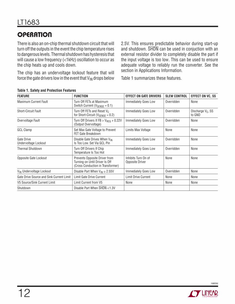
Table 1 summarizes these features.
Table 1. Safety and Protection FeaturesFEATURE FUNCTION EFFECT ON GATE DRIVERS SLEW CONTROL EFFECT ON VC, SS
Maximum Current Fault Turn Off FETs at Maximum Switch Current (VSENSE = 0.1)
Immediately Goes Low Overridden None
Short-Circuit Fault Turn Off FETs and Reset VC for Short-Circuit (VSENSE = 0.2)
Immediately Goes Low Overridden Discharge VC, SS to GND
Overvoltage Fault Turn Off Drivers If FB > VREG + 0.22V (Output Overvoltage)
Immediately Goes Low Overridden None
GCL Clamp Set Max Gate Voltage to Prevent FET Gate Breakdown
Limits Max Voltage None None
Gate Drive Undervoltage Lockout
Disable Gate Drives When VIN Is Too Low. Set Via GCL Pin
Immediately Goes Low Overridden None
Thermal Shutdown Turn Off Drivers If Chip Temperature Is Too Hot
Immediately Goes Low Overridden None
Opposite Gate Lockout Prevents Opposite Driver from Turning on Until Driver Is Off (Cross Conduction in Transformer)
Inhibits Turn On of Opposite Driver
None None
VIN Undervoltage Lockout Disable Part When VIN ≅ 2.55V Immediately Goes Low Overridden None
Gate Drive Source and Sink Current Limit Limit Gate Drive Current Limit Drive Current None None
V5 Source/Sink Current Limit Limit Current from V5 None None None
Shutdown Disable Part When SHDN <1.3V
LT1683
131683fd
Reducing EMI from switching power supplies has tradition-ally invoked fear in designers. Many switchers are designed solely on efficiency and as such produce waveforms filled with high frequency harmonics that then propagate through the rest of the system.
The LT1683 provides control over two of the more impor-tant variables for controlling EMI with switching inductive loads: switch voltage slew rate and switch current slew rate. The use of this part will reduce noise and EMI over conventional switch mode controllers. Because these variables are under control, a supply built with this part will exhibit far less tendency to create EMI and less chance of encountering problems during production.
It is beyond the scope of this data sheet to get into EMI fundamentals. Application Note 70 contains much informa-tion concerning noise in switching regulators and should be consulted.
Oscillator Frequency
The oscillator determines the switching frequency and therefore the fundamental positioning of all harmonics. The use of good quality external components is important to ensure oscillator frequency stability. The oscillator is of a sawtooth design. A current defined by external resistor, RT, is used to charge and discharge the capacitor, CT . The discharge rate is approximately ten times the charge rate.
By allowing the user to have control over both compo-nents, trimming of oscillator frequency can be more easily achieved.
The external capacitance CT is chosen by:
CT(nF) = 2180
f(kHz) •RT(kΩ)
where f is the desired oscillator frequency in kHz. For RT equal to 16.9k, this simplifies to:
CT(nF) = 129
f(kHz)
e.g., CT = 1.29nF for f = 100kHz
APPLICATIONS INFORMATIONNominally RT should be 16.9k. Since it sets up current, its temperature coefficient should be selected to compliment the capacitor. Ideally, both should have low temperature coefficients.
Oscillator frequency is important for noise reduction in two ways. First the lower the oscillator frequency the lower the waveform’s harmonics, making it easier to filter them. Second the oscillator will control the placement of the output voltage harmonics which can aid in specific problems where you might be trying to avoid a certain frequency bandwidth.
Oscillator Sync
If a more precise frequency is desired (e.g., to accurately place harmonics) the oscillator can be synchronized to an external clock. Set the RC timing components for an oscillator frequency 10% lower than the desired sync frequency.
Drive the SYNC pin with a square wave (with greater than 1.4V amplitude). The rising edge of the sync square wave will initiate clock discharge. The sync pulse should have a minimum pulse width of 0.5µs.
Be careful in sync’ing to frequencies much different from the part since the internal oscillator charge slope determines slope compensation. It would be possible to get into subharmonic oscillation if the sync doesn’t al-low for the charge cycle of the capacitor to initiate slope compensation. In general, this will not be a problem until the sync frequency is greater than 1.5 times the oscillator free-run frequency.
Slew Rate Setting
The primary reason to use this part is to gain advantage of lower EMI and noise due to slew control. The rolloff in higher frequency harmonics has its theoretical basis with two primary components. First, the clock frequency sets the fundamental positioning of harmonics and second, the associated normal frequency rolloff of harmonics.
LT1683
141683fd
APPLICATIONS INFORMATIONThis part creates a second higher frequency rolloff of harmonics that inversely depends on the slew time, the time that voltage or current spends between the off state and on state. This time is adjustable through the choice of the slew resistors, the external resistors to ground on the RVSL and RCSL pins and the external components used for the external voltage feedback capacitors CAV, CBV (from CAP A or CAP B to their respective MOSFET drains) and the sense resistor. Lower slew rates (longer slew times, lower frequency for harmonics rolloff) is created with higher values of RVSL, RCSL, CAV, CBV and the current sense resistor.
Setting the voltage and current slew rates should be done empirically. The most practical way of determining these components is to set CAV, CBV and the sense resistor value. Then, start by making RVSL, RCSL each a 50k resistor pot in series with 3.3k. Starting from the lowest resistor set-ting (fast slew) adjust the pots until the noise level meets your guidelines. Note that slower slewing waveforms will dissipate more power so that efficiency will drop. You can monitor this as you make your slew adjustment by measuring input and output voltage and their respective currents. Monitor the MOSFET temperature as slew rates are slowed. These components will heat up as efficiency decreases.
Measuring noise should be done carefully. It is easy to introduce noise by poor measurement techniques. Consult AN70 for recommended measurement techniques. Keeping probe ground leads very short is essential.
Usually it will be desirable to keep the voltage and cur-rent slew resistors approximately the same. There are circumstances where a better optimization can be found by adjusting each separately, but as these values are separated further, a loss of independence of control may occur.
It is possible to use a single slew setting resistor. In this case the RVSL and RCSL pins are tied together. A resistor with a value of 1.8k to 34k (one-half the individual resis-tors) can then be tied from these pins to ground.
In general only the RCSL value will be available for adjust-ment of current slew. The current slew time does also depend on the current sense resistor but this resistor is
normally set with consideration of the maximum current in the MOSFETs.
Setting the voltage slew also involves selection of the capacitors CAV, CBV. The voltage slew time is proportional to the output voltage swing (basically input voltage), the external voltage feedback capacitor and the RVSL value. Thus at higher input voltages smaller capacitors will be used with lower RVSL values. For a starting point use Table 2.
Table 2INPUT VOLTAGE CAPACITOR VALUE
<25V 5pF
50V 2.5pF
100V 1pF
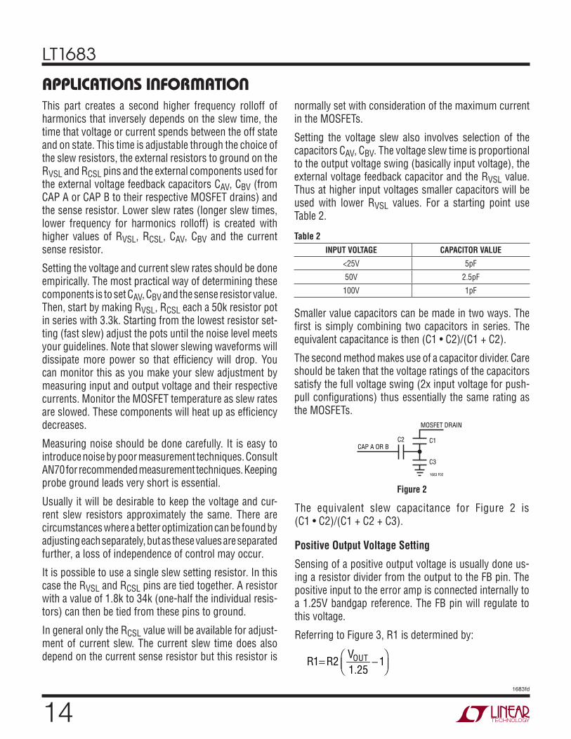
Smaller value capacitors can be made in two ways. The first is simply combining two capacitors in series. The equivalent capacitance is then (C1 • C2)/(C1 + C2).
The second method makes use of a capacitor divider. Care should be taken that the voltage ratings of the capacitors satisfy the full voltage swing (2x input voltage for push-pull configurations) thus essentially the same rating as the MOSFETs.
C1
MOSFET DRAIN
C2CAP A OR B
C3
1683 F02
Figure 2
The equivalent slew capacitance for Figure 2 is (C1 • C2)/(C1 + C2 + C3).
Positive Output Voltage Setting
Sensing of a positive output voltage is usually done us-ing a resistor divider from the output to the FB pin. The positive input to the error amp is connected internally to a 1.25V bandgap reference. The FB pin will regulate to this voltage.
Referring to Figure 3, R1 is determined by:
R1= R2
VOUT1.25
− 1
LT1683
151683fd
APPLICATIONS INFORMATIONThe FB bias current represents a small error and can usually be ignored for values of R1||R2 up to 10k.
One word of caution, sometimes a feedback zero is added to the control loop by placing a capacitor across R1. If the feedback capacitively pulls the FB pin above the in-ternal regulator voltage (2.4V), output regulation may be disrupted. A series resistance with the feedback pin can eliminate this potential problem. There is an internal clamp on FB that clamps at 0.7V above the regulation voltage that should also help prevent this problem.
NFB PIN
INFB
1683 F04
–VOUT
R2
R1
FB PIN
1683 F03
VOUT
R2
R1
Figure 3
Figure 4
Negative Output Voltage Setting
Negative output voltage can be sensed using the NFB pin. In this case regulation will occur when the NFB pin is at –2.5V. The nominal input bias current for the NFB is –25µA (INFB), which needs to be accounted for in setting up the divider.
Referring to Figure 4, R1 is chosen such that:
R1= R2
VOUT − 2.52.5 + R2 •25µA
A suggested value for R2 is 2.5k. The NFB pin is normally left open if the FB pin is being used.
Dual Polarity Output Voltage Sensing
Certain applications may benefit from sensing both posi-tive and negative output voltages. When doing this each output voltage resistor divider is individually set as previ-ously described. When both FB and NFB pins are used,
the LT1683 will act to prevent either output from going beyond its set output voltage. The highest output (lightest load) will dominate control of the regulator. This technique would prevent either output from going unregulated high at no load. However, this technique will also compromise output load regulation.
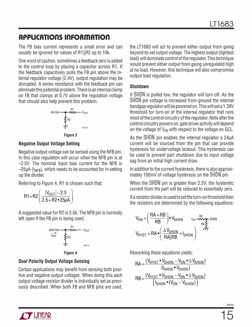
Shutdown
If SHDN is pulled low, the regulator will turn off. As the SHDN pin voltage is increased from ground the internal bandgap regulator will be powered on. This will set a 1.39V threshold for turn-on of the internal regulator that runs most of the control circuitry of the regulator. Note after the control circuitry powers on, gate driver activity will depend on the voltage of VIN with respect to the voltage on GCL.
As the SHDN pin enables the internal regulator a 24µA current will be sourced from the pin that can provide hysteresis for undervoltage lockout. This hysteresis can be used to prevent part shutdown due to input voltage sag from an initial high current draw.
In addition to the current hysteresis, there is also approxi-mately 100mV of voltage hysteresis on the SHDN pin.
When the SHDN pin is greater than 2.2V, the hysteretic current from the part will be reduced to essentially zero.
If a resistor divider is used to set the turn-on threshold then the resistors are determined by the following equations:
VON = RA + RBRB
• VSHDN
VHYST = RA •∆ VSHDNRA RB
+ISHDN
Reworking these equations yields:
RA =(VHYST • VSHDN − VON • ∆ VSHDN)
(ISHDN • VSHDN)
RB =(VHYST • VSHDN − VON • ∆ VSHDN)
ISHDN •(VON − VSHDN)
VINRA
RB
SHDN
LT1683
161683fd
APPLICATIONS INFORMATIONSo if we wanted to turn on at 20V with 2V of hysteresis:
RA = 2V •1.39V − 20V •0.1V24µA •1.39V
= 23.4k
RB = 2V •1.39V − 20V •0.1V24µA •(20V − 1.39V)
= 1.75k
Resistor values could be altered further by adding Zeners in the divider string. A resistor in series with SHDN pin could further change hysteresis without changing turn-on voltage.
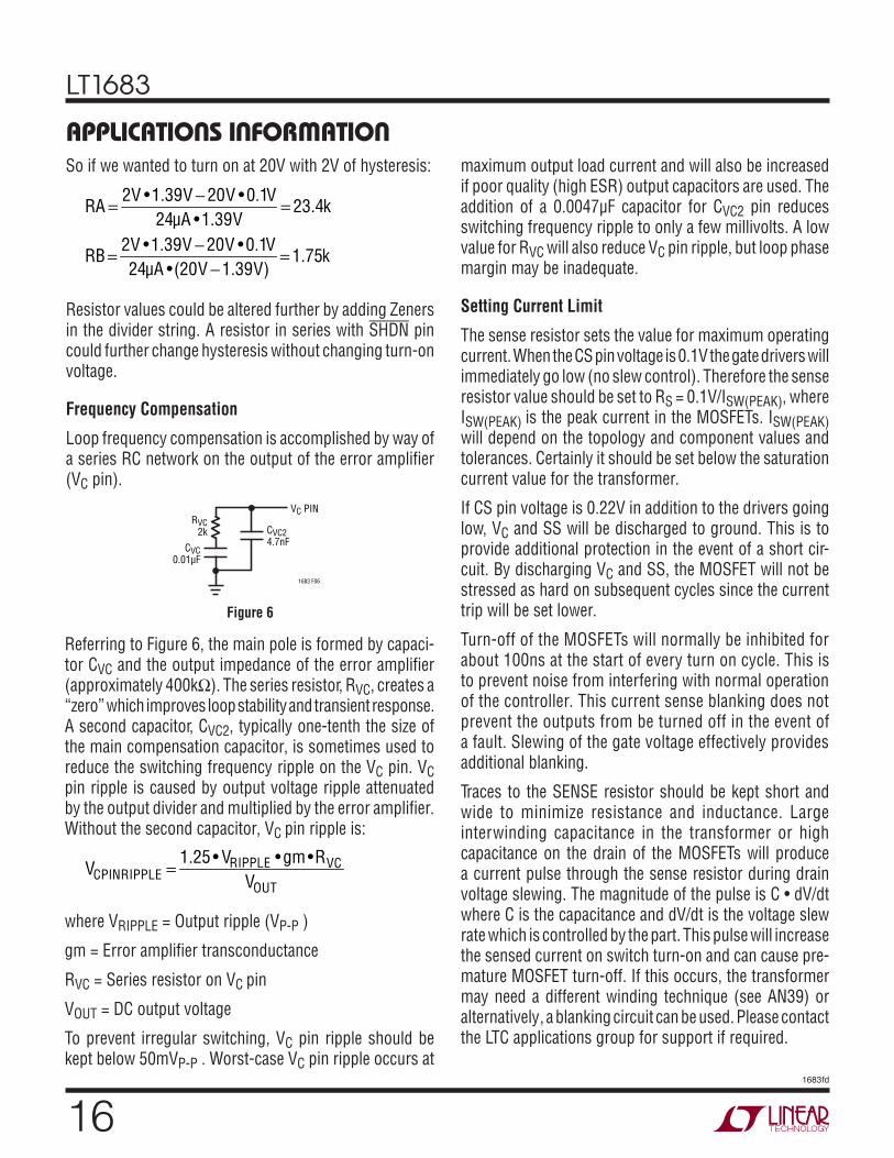
Frequency Compensation
Loop frequency compensation is accomplished by way of a series RC network on the output of the error amplifier (VC pin).
VC PIN
1683 F06
RVC2k
CVC0.01µF
CVC24.7nF
Figure 6
Referring to Figure 6, the main pole is formed by capaci-tor CVC and the output impedance of the error amplifier (approximately 400kΩ). The series resistor, RVC, creates a “zero” which improves loop stability and transient response. A second capacitor, CVC2, typically one-tenth the size of the main compensation capacitor, is sometimes used to reduce the switching frequency ripple on the VC pin. VC pin ripple is caused by output voltage ripple attenuated by the output divider and multiplied by the error amplifier. Without the second capacitor, VC pin ripple is:
VCPINRIPPLE =
1.25 • VRIPPLE •gm •RVCVOUT
where VRIPPLE = Output ripple (VP-P )
gm = Error amplifier transconductance
RVC = Series resistor on VC pin
VOUT = DC output voltage
To prevent irregular switching, VC pin ripple should be kept below 50mVP-P . Worst-case VC pin ripple occurs at
maximum output load current and will also be increased if poor quality (high ESR) output capacitors are used. The addition of a 0.0047µF capacitor for CVC2 pin reduces switching frequency ripple to only a few millivolts. A low value for RVC will also reduce VC pin ripple, but loop phase margin may be inadequate.
Setting Current Limit
The sense resistor sets the value for maximum operating current. When the CS pin voltage is 0.1V the gate drivers will immediately go low (no slew control). Therefore the sense resistor value should be set to RS = 0.1V/ISW(PEAK), where ISW(PEAK) is the peak current in the MOSFETs. ISW(PEAK) will depend on the topology and component values and tolerances. Certainly it should be set below the saturation current value for the transformer.
If CS pin voltage is 0.22V in addition to the drivers going low, VC and SS will be discharged to ground. This is to provide additional protection in the event of a short cir-cuit. By discharging VC and SS, the MOSFET will not be stressed as hard on subsequent cycles since the current trip will be set lower.
Turn-off of the MOSFETs will normally be inhibited for about 100ns at the start of every turn on cycle. This is to prevent noise from interfering with normal operation of the controller. This current sense blanking does not prevent the outputs from be turned off in the event of a fault. Slewing of the gate voltage effectively provides additional blanking.
Traces to the SENSE resistor should be kept short and wide to minimize resistance and inductance. Large interwinding capacitance in the transformer or high capacitance on the drain of the MOSFETs will produce a current pulse through the sense resistor during drain voltage slewing. The magnitude of the pulse is C • dV/dt where C is the capacitance and dV/dt is the voltage slew rate which is controlled by the part. This pulse will increase the sensed current on switch turn-on and can cause pre-mature MOSFET turn-off. If this occurs, the transformer may need a different winding technique (see AN39) or alternatively, a blanking circuit can be used. Please contact the LTC applications group for support if required.
LT1683
171683fd
Soft-Start
The soft-start pin is used to provide control of switching current during start-up. The max voltage on the VC pin is approximately the voltage on the SS pin. A current source will linearly charge a capacitor on the SS pin. The VC pin voltage will thus ramp also. The approximate time for the voltage on these pins to ramp is (1.31V/9µA) • CSS or approximately 146ms per µF.
The soft-start current will be initiated as soon as the part turns on. Soft-start will be reinititated after a short-circuit fault.
Thermal Considerations
Most of the IC power dissipation is derived from the VIN pin. The VIN current depends on a number of factors in-cluding: oscillator frequency; loads on V5; slew settings; gate charge current. Additional power is dissipated if V5 sinks current and during the MOSFET gate discharge.
The power dissipation in the IC will be the sum of:
1) The RMS VIN current times VIN
2) V5 RMS sink current times 5V
3) The gate drive’s RMS discharge current times voltage
Because of the strong VIN component it is advantageous to operate the LT1683 at as low a VIN as possible.
It is always recommended that package temperature be measured in each application. The part has an internal thermal shutdown to minimize the chance of IC destruction but this should not replace careful thermal design.
The thermal shutdown feature does not protect the external MOSFETs. A separate analysis must be done for those devices to ensure that they are operating within safe limits.
Once IC power dissipation, PDIS, is determined die junction temperature is then computed as:
TJ = TAMB + PDIS • θJA
where TAMB is ambient temperature and θJA is the package thermal resistance. For the 20-pin SSOP, θJA is 100°C/W.
APPLICATIONS INFORMATIONMagnetics
Design of magnetics is dependent on topology. The fol-lowing details the design of the magnetics for a push-pull converter. In this converter the transformer usually stores little energy. The following equations should be considered as the starting point to building a prototype.
The following definitions will be used:
VIN = Input supply voltage
RON = Switch-on resistance
ISW = Maximum switch current
VOUT = Desired output voltage
IOUT = Output current
f = Oscillator frequency
VF = Forward drop of the rectifier
Duty cycle is the major defining equation for this topology. Note that the output L and C basically filter the chopped voltage so duty cycle controls output voltage. N is the turns ratio of the transformer. The turns ratio must be large enough to ensure that the transformer can put out a voltage equal to the output voltage plus the diode under minimum input conditions. Note the transformer operates at half the oscillator frequency (f).
N =VOUT + VF
2 •DCMAX( ) VIN(MIN) −ISW RON + RSENSE( )
DCMAX is the maximum duty cycle of each driver with respect to the entire cycle, which consists of two periods (A on and B on). So the effective duty cycle is 2 • DCMAX. The controller, in general, determines maximum duty cycle. A 44% maximum duty cycle is a guaranteed value for this part.
Remember to add sufficient margin in the turns ratio to account for IR drops in the transformer windings, worst-case diode forward drops and switch-on voltage. Also at very slow slew rates the effective DC may be reduced.
LT1683
181683fd
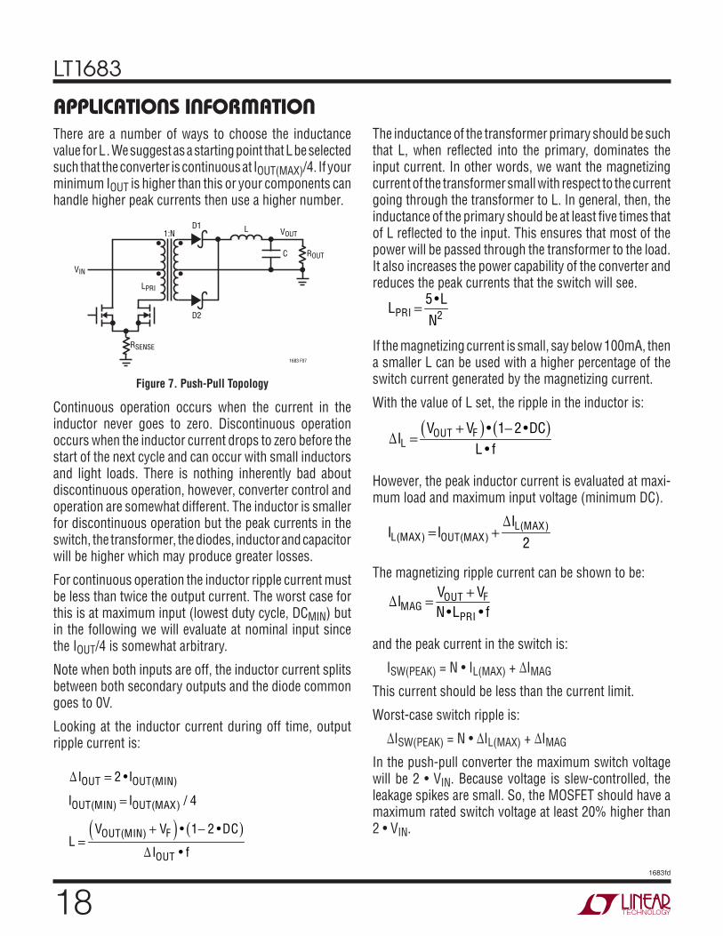
There are a number of ways to choose the inductance value for L. We suggest as a starting point that L be selected such that the converter is continuous at IOUT(MAX)/4. If your minimum IOUT is higher than this or your components can handle higher peak currents then use a higher number.
APPLICATIONS INFORMATION
1:N
LPRI
D2
D1 L
C ROUT
RSENSE
VOUT
VIN
1683 F07
Figure 7. Push-Pull Topology
Continuous operation occurs when the current in the inductor never goes to zero. Discontinuous operation occurs when the inductor current drops to zero before the start of the next cycle and can occur with small inductors and light loads. There is nothing inherently bad about discontinuous operation, however, converter control and operation are somewhat different. The inductor is smaller for discontinuous operation but the peak currents in the switch, the transformer, the diodes, inductor and capacitor will be higher which may produce greater losses.
For continuous operation the inductor ripple current must be less than twice the output current. The worst case for this is at maximum input (lowest duty cycle, DCMIN) but in the following we will evaluate at nominal input since the IOUT/4 is somewhat arbitrary.
Note when both inputs are off, the inductor current splits between both secondary outputs and the diode common goes to 0V.
Looking at the inductor current during off time, output ripple current is:
∆IOUT = 2 • IOUT(MIN)
IOUT(MIN) = IOUT(MAX) / 4
L =VOUT(MIN) + VF( ) • 1− 2 •DC( )
∆IOUT • f
The inductance of the transformer primary should be such that L, when reflected into the primary, dominates the input current. In other words, we want the magnetizing current of the transformer small with respect to the current going through the transformer to L. In general, then, the inductance of the primary should be at least five times that of L reflected to the input. This ensures that most of the power will be passed through the transformer to the load. It also increases the power capability of the converter and reduces the peak currents that the switch will see.
LPRI = 5 •L
N2
If the magnetizing current is small, say below 100mA, then a smaller L can be used with a higher percentage of the switch current generated by the magnetizing current.
With the value of L set, the ripple in the inductor is:
∆IL =
VOUT + VF( ) • 1− 2 •DC( )L • f
However, the peak inductor current is evaluated at maxi-mum load and maximum input voltage (minimum DC).
IL(MAX) = IOUT(MAX) +
∆IL(MAX)
2
The magnetizing ripple current can be shown to be:
∆IMAG =
VOUT + VFN •LPRI • f
and the peak current in the switch is:
ISW(PEAK) = N • IL(MAX) + ∆IMAG
This current should be less than the current limit.
Worst-case switch ripple is:
∆ISW(PEAK) = N • ∆IL(MAX) + ∆IMAG
In the push-pull converter the maximum switch voltage will be 2 • VIN. Because voltage is slew-controlled, the leakage spikes are small. So, the MOSFET should have a maximum rated switch voltage at least 20% higher than 2 • VIN.
LT1683
191683fd
APPLICATIONS INFORMATIONSo, given the turns ratio, primary inductance and cur-rent, the transformer can be designed. The design of the transformer will require analyzing the power losses of the transformer and making necessary adjustments.
Most transformer companies can assist you with designing an optimal solution. For instance Midcom, Inc. (1-800-643-2661). Linear Technology’s application group can also help.
As an example say we are designing a 48V ±20% to 5V 100kHz converter with 2A output and 500mA ripple. Then starting with a guess for the on voltage of the MOSFET plus sense resistor of 0.5V and VF of 0.5V:
N = 5 + 0.5
88% • 48 •80% − 0.5( ) = 16.1
For continuous operation at IOUT(MIN) = IOUT(MAX)/4, inductor ripple (the same as output ripple):
∆IL = 2 •
2A4
= 1A
The duty cycle for nominal input is:
DCNOM =VOUT + VF
2 •N VIN(NOM) −ISW •RON( )= 5.5
26.1
• 47.5= 35.3%
Then:
L =
5 + 0.5( ) • 1− 2 •35.3%( )1A •100kHz
= 16µH
Off-the-shelf components can be used for this inductor. Say we choose a 22µH inductor, then ripple current at maximum input (DC = 29.1%) is:
∆IL =
5 + 0.5( ) • 1− 2 •29.1%( )22µF •100kHz
= 1.03A
The maximum inductor current is:
IL(MAX) = 2A + 1.03A
2= 2.52A
Primary inductance should be greater than:
LPRI = 5 • 22µH • 6.12 = 4.1mH
The secondary inductance would then be:
4.1mH/6.12 = 110µH
The magnetizing ripple current is approximately:
∆IMAG = 5.51
6.1• 4.1mH •100kHz
= 81mA
Peak switch current is:
ISW(PEAK) = 1
6.1•2.51A + 81mA = 494mA
Note that you can discern your magnetizing ripple by looking at the reflected inductance ripple and subtracting it from the switch current ripple.
∆IMAG = ∆ISW – N • ILThe max ripple current on the switch is:
∆ISW(MAX) = 1.03A
6.1+ 81mA = 0.25A
Knowing the peak switch current we can go back and iterate with a more accurate switch-on voltage. We would have to know the RON of the FET. In our case our assumptions of a 0.5V switch-on voltage is valid for RON + RSENSE < 1Ω.
Capacitors
Correct choice of input and output capacitors is very important to low noise switcher performance. Push-pull topologies and other low noise topologies will in general have continuous currents, which reduce the requirements
LT1683
201683fd
APPLICATIONS INFORMATIONfor capacitance. However, noise depends more on the ESR of the capacitors. In addition lower ESR can also improve efficiency.
Input capacitors must also withstand surges that occur during the switching of some types of loads. Some solid tan-talum capacitors can fail under these surge conditions.
Design Note 95 offers more information but the following is a brief summary of capacitor types and attributes.
Aluminum Electrolytic: Low cost and higher voltage. They can be used in this application but in general you will need higher capacitance to achieve low ESR. Additional nonelectrolytic capacitors may be required to achieve better performance.
Specialty Polymer Aluminum: Panasonic has come out with their series CD capacitors. While they are only avail-able for voltages below 16V, they have very low ESR and good surge capability.
Solid Tantalum: Small size and low impedance. Typically the maximum voltage rating is 50V. With large surge cur-rents the capacitor may need to be derated or you need a special type such as AVX TPS line.
OS-CON: Lower impedance than aluminum but only avail-able for 35V or less. Form factor may be a problem.
Ceramic: Generally used for high frequency and high voltage bypass. They may resonate with their ESL before ESR becomes dominant. Recent multilayer ceramic (MLC) capacitors provide larger capacitance with low ESR.
There are continuous improvements being made in ca-pacitors so consult with manufacturers as to your specific needs.
Input Capacitors
The input capacitor should have low ESR at high frequen-cies since this will be an important factor concerning how much conducted noise is created.
There are two separate requirements for input capacitors. The first is for supply to the part’s VIN pin. The VIN pin will provide current for the part itself and the gate charge current.
The worst component from an AC point is the gate charge current. The actual peak current depends on gate capaci-tance and slew rate, being higher for larger values of each. The total current can be estimated by gate charge and frequency of operation. Because of the slewing with this part, gate charge is spread out over a longer time period than with a normal FET driver. This reduces capacitance requirements.
Typically the current will have spikes of under 100mA located at the gate voltage transitions. This is charge/dis-charge to and from the threshold voltage. Most slewing occurs with the gate voltage near threshold.
Since the part’s VIN will typically be under 15V many op-tions are available for choice of capacitor. Values of input capacitor for just VIN requirement will typically be in the 50µF range with an ESR of under 0.1Ω.
In addition to the part supply, decoupling of the supply to the transformer needs to be considered. If this is the same supply as the VIN pin then that capacitor will need to be increased. However, often with this part the transformer supply will be a higher voltage and as such a separate capacitor.
The transformer decoupling capacitor will see the switch current as ripple.
This switch current computation can be used to estimate the capacity for these capacitors:
CIN = 1∆ VCAP
∆ISW(MAX)− ESR
•DCMIN
f
where ∆VCAP is the allowed sag on the input capacitor. ESR is the equivalent series resistance for the cap. In general allowed sag will be a few tenths of volts.
Output Filter Capacitor
The output capacitor is chosen both for capacity and ESR. The capacity must supply the load current in the switch-off state. While slew control reduces higher frequency components of the ripple current in the capacitor, the capacitor ESR and the magnitude of the output ripple
LT1683
211683fd
APPLICATIONS INFORMATIONcurrent controls the fundamental component. ESR should also be low to reduce capacitor dissipation.
The capacitance value can be computed by consideration of desired load ripple, duty cycle and ESR.
COUT = 1∆ VOUT
∆IL(MAX)− ESR
•DCMIN
f
MOSFET Selection
There is a wide variety of MOSFETs to choose from for this part. The part will work with either normal threshold (3V to 4V) or logic-level threshold devices (1V to 2V).
Select a voltage rating to ensure under worst-case condi-tions that the MOSFET will not break down. Next choose an RON sufficiently low to meet both the power dissipation capabilities of the MOSFET package as well as overall ef-ficiency needs of the converter.
The LT1683 can handle a large range of gate charges. However at very large charge stability may be affected.
The power dissipation in the MOSFET depends on several factors. The primary element is I2R heating when the device is on. In addition, power is dissipated when the device is slewing. An estimate for power dissipation is:
P VI
I
I
V R II
INSR
IN ON
=+
+
− +⎛
⎝⎜⎞
⎠⎟⎡
⎣⎢⎢
⎤
•
Δ •• Δ
22 2 2 2
2
4
34 ⎦⎦
⎥⎥
⎧
⎨
⎪⎪
⎩
⎪⎪
⎫
⎬
⎪⎪
⎭
⎪⎪
+
VI
f I R DC
SR
ON
•
• • •2
where I is the average current, ∆I is the ripple current in the switch, ISR is the current slew rate, VSR is the voltage slew rate, f is the oscillator frequency, DC is the duty cycle and RON is the MOSFET on-resistance.
Setting GCL Voltage
Setting the voltage on the GCL pin depends on what type of MOSFET is used and the desired gate drive undervoltage lockout voltage.
First determine the maximum gate drive that you require. Typically you will want it to be at least 2V greater than the maximum threshold. Higher voltages will lower the on resistance and increase efficiency. Be certain to check the maximum allowed gate voltage. Often this is 20V but for some logic threshold MOSFETs it is only 8V to 10V.
VGCL needs to be set approximately 0.2V above the desired max gate threshold. In addition VIN needs to be at least 1.6V above the gate voltage.
The GCL pin can be tied to VIN which will result in a maxi-mum gate voltage of VIN – 1.6V.
This pin also controls undervoltage lockout of the gate drives. The undervoltage lockout will prevent the MOSFETs from switching until there is sufficient drive present.
If GCL is tied to a voltage source or Zener less than 6.8V, the gate drivers will not turn on until VIN exceeds the GCL voltage by 0.8V. For VGCL above 6.5V, the gate drives are ensured to be off for VIN < 7.3V and they will be turned on by VGCL + 0.8V.
If GCL is tied to VIN, the gate drivers are always on (undervoltage lockout is disabled).
Approximately 50µA of current can be sourced from this pin if VIN > VGCL + 0.8V. This could be used to bias a Zener.
The GCL pin has an internal 19V Zener to ground that will provide a failsafe for maximum gate voltage.
As an example say we are using a Siliconix Si4480DY which has RDS(ON) rated at 6V. To get 6V, VGCL needs to be set to 6.2V and VIN needs to be at least 7.6V.
LT1683
221683fd
APPLICATIONS INFORMATIONGate Driver Considerations
In general, the MOSFETs should be positioned as close to the part as possible to minimize inductance.
When the part is active the gate drives will be pulled low to less than 0.2V. When the part is off, the gate drives contain a 40k resistor in series with a diode to ground that will offer passive holdoff protection. If you are using some logic-level MOSFETs this might not be sufficient. A resistor may be placed from gate to ground, however the value should be reasonably high to minimize DC losses and possible AC issues.
The gate drive source current comes from VIN. The sink current exits through PGND. In general the decoupling cap should be placed close to these two pins.
Switching Diodes
In general, switching diodes should be Schottky diodes. Size and breakdown voltage depend on the specific converter. A lower forward drop will improve converter efficiency. No other special requirements are needed.
PCB Layout Considerations
As with any switcher careful consideration should be given to PC board layout. Because this part reduces high frequency EMI the board layout is less critical, however high currents and voltages still produce the need for careful board layout to eliminate poor and erratic performance.
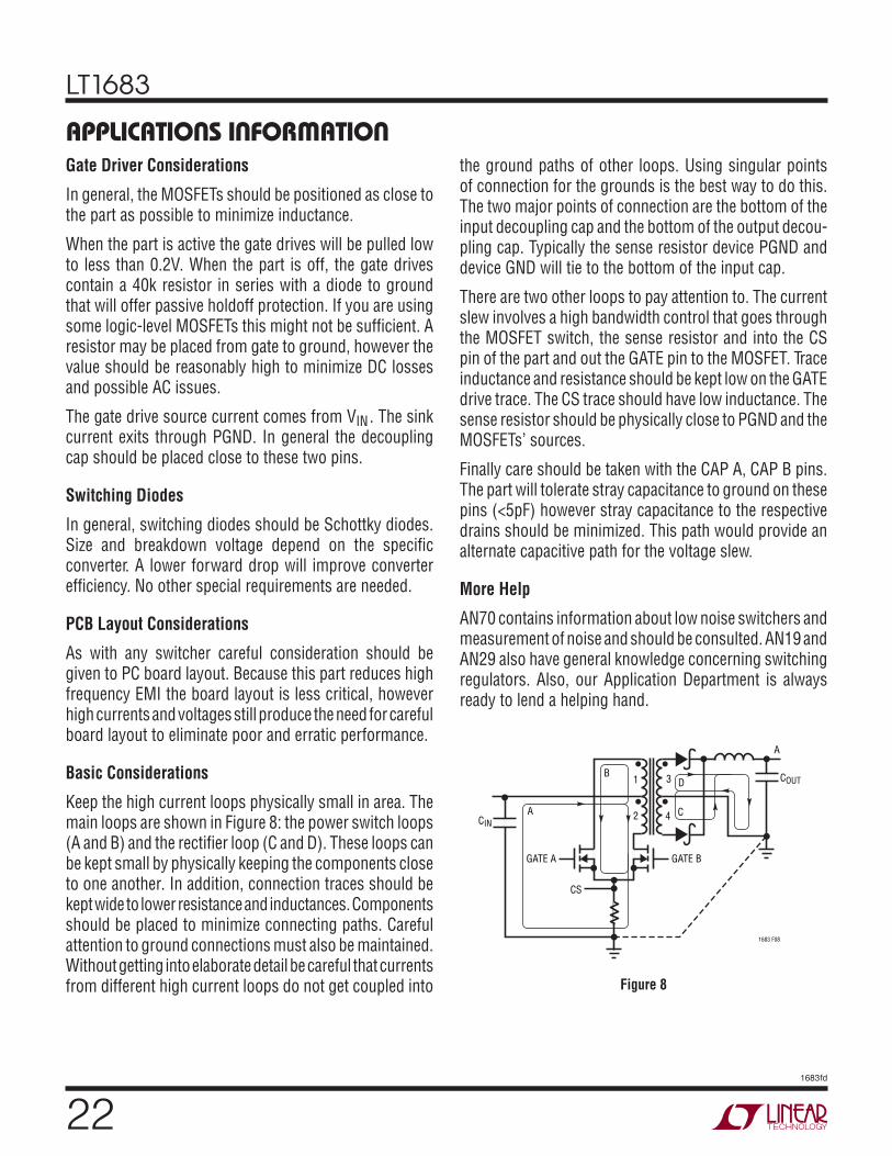
Basic Considerations
Keep the high current loops physically small in area. The main loops are shown in Figure 8: the power switch loops (A and B) and the rectifier loop (C and D). These loops can be kept small by physically keeping the components close to one another. In addition, connection traces should be kept wide to lower resistance and inductances. Components should be placed to minimize connecting paths. Careful attention to ground connections must also be maintained. Without getting into elaborate detail be careful that currents from different high current loops do not get coupled into
the ground paths of other loops. Using singular points of connection for the grounds is the best way to do this. The two major points of connection are the bottom of the input decoupling cap and the bottom of the output decou-pling cap. Typically the sense resistor device PGND and device GND will tie to the bottom of the input cap.
There are two other loops to pay attention to. The current slew involves a high bandwidth control that goes through the MOSFET switch, the sense resistor and into the CS pin of the part and out the GATE pin to the MOSFET. Trace inductance and resistance should be kept low on the GATE drive trace. The CS trace should have low inductance. The sense resistor should be physically close to PGND and the MOSFETs’ sources.
Finally care should be taken with the CAP A, CAP B pins. The part will tolerate stray capacitance to ground on these pins (<5pF) however stray capacitance to the respective drains should be minimized. This path would provide an alternate capacitive path for the voltage slew.
More Help
AN70 contains information about low noise switchers and measurement of noise and should be consulted. AN19 and AN29 also have general knowledge concerning switching regulators. Also, our Application Department is always ready to lend a helping hand.
1683 F08
1
2 4
3
CIN
COUT
A
A
B
CS
GATE A GATE B
D
C
Figure 8
LT1683
231683fd
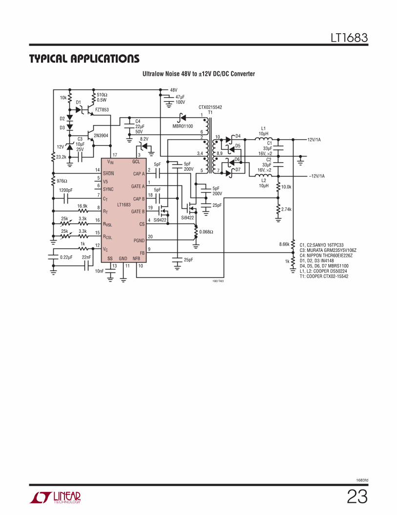
TYPICAL APPLICATIONSUltralow Noise 48V to ±12V DC/DC Converter
L110µH
C233µF
16V, ×2
C133µF
16V, ×2
MBR01100
L210µH
3
10
1683 TA03
1113
SHDN CAP A
NFB
LT1683
GND
VIN
17
14 2
GCL
SS
V5
SYNCGATE A
51
CT CAP B
6
18
RT GATE B
7
198
RCSL
16
VC
15
12
RVSL CS4
PGND20
FB9
5pF
5pF
Si9422Si9422
0.068Ω
976Ω
23.2k
10nF
1k
3.3k
25k
25k
3.3k
16.9k
1200pF
47µF100V
48V
C310µF25V12V
8.2V
10k510Ω0.5W
2N3904
C422µF50V
25pF22nF0.22µF
8.66k
1k
2.74k
10.0k
FZT853
5pF200V
25pF
5pF200V
–12V/1A
12V/1A
D1
D4
D5
D7
D6
D2
D3
CTX0215542T11
2
3,4
5
6
7
8,9
10
C1, C2:SANYO 16TPC33C3: MURATA GRM235Y5V106ZC4: NIPPON THCR60EIE226ZD1, D2, D3 IN4148D4, D5, D6, D7 MBRS1100L1, L2: COOPER DS50224 T1: COOPER CTX02-15542
LT1683
241683fd
PACKAGE DESCRIPTIONG Package
20-Lead Plastic SSOP (5.3mm)(Reference LTC DWG # 05-08-1640)
G20 SSOP 0204
0.09 – 0.25(.0035 – .010)
0 – 8
0.55 – 0.95(.022 – .037)
5.00 – 5.60**(.197 – .221)
7.40 – 8.20(.291 – .323)
1 2 3 4 5 6 7 8 9 10
6.90 – 7.50*(.272 – .295 )1718 14 13 12 1115161920
2.0(.079)MAX
0.05(.002)MIN
0.65(.0256)
BSC0.22 – 0.38
(.009 – .015)TYPMILLIMETERS
(INCHES)
DIMENSIONS DO NOT INCLUDE MOLD FLASH. MOLD FLASH SHALL NOT EXCEED .152mm (.006") PER SIDEDIMENSIONS DO NOT INCLUDE INTERLEAD FLASH. INTERLEAD FLASH SHALL NOT EXCEED .254mm (.010") PER SIDE
*
**
NOTE:1. CONTROLLING DIMENSION: MILLIMETERS
2. DIMENSIONS ARE IN
3. DRAWING NOT TO SCALE
0.42 0.03 0.65 BSC
5.3 – 5.77.8 – 8.2
RECOMMENDED SOLDER PAD LAYOUT
1.25 0.12
LT1683
251683fd
Information furnished by Linear Technology Corporation is believed to be accurate and reliable. However, no responsibility is assumed for its use. Linear Technology Corporation makes no representa-tion that the interconnection of its circuits as described herein will not infringe on existing patent rights.
REVISION HISTORYREV DATE DESCRIPTION PAGE NUMBER
D 11/10 Updated Max Switch Frequency to 150kHz in the Electrical Characteristics section 3
(Revision history begins at Rev D)
LT1683
261683fd
Linear Technology Corporation1630 McCarthy Blvd., Milpitas, CA 95035-7417 (408) 432-1900 FAX: (408) 434-0507 www.linear.com LINEAR TECHNOLOGY CORPORATION 2001
LT 1110 REV D • PRINTED IN USA
RELATED PARTS
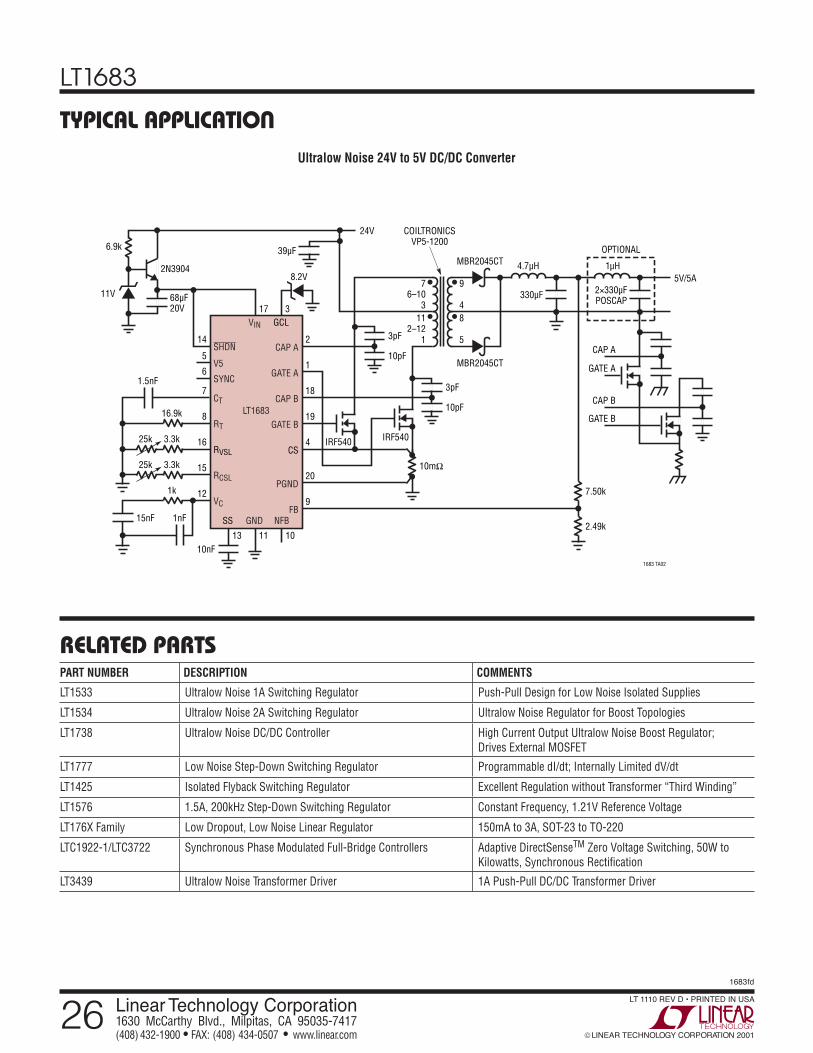
TYPICAL APPLICATION
PART NUMBER DESCRIPTION COMMENTS
LT1533 Ultralow Noise 1A Switching Regulator Push-Pull Design for Low Noise Isolated Supplies
LT1534 Ultralow Noise 2A Switching Regulator Ultralow Noise Regulator for Boost Topologies
LT1738 Ultralow Noise DC/DC Controller High Current Output Ultralow Noise Boost Regulator; Drives External MOSFET
LT1777 Low Noise Step-Down Switching Regulator Programmable dI/dt; Internally Limited dV/dt
LT1425 Isolated Flyback Switching Regulator Excellent Regulation without Transformer “Third Winding”
LT1576 1.5A, 200kHz Step-Down Switching Regulator Constant Frequency, 1.21V Reference Voltage
LT176X Family Low Dropout, Low Noise Linear Regulator 150mA to 3A, SOT-23 to TO-220
LTC1922-1/LTC3722 Synchronous Phase Modulated Full-Bridge Controllers Adaptive DirectSenseTM Zero Voltage Switching, 50W to Kilowatts, Synchronous Rectification
LT3439 Ultralow Noise Transformer Driver 1A Push-Pull DC/DC Transformer Driver
MBR2045CT
COILTRONICSVP5-1200
4.7µH
330µF
CAP A
CAP B
GATE A
GATE B
MBR2045CT
1µH
OPTIONAL
5V/5A2×330µFPOSCAP
3
10
1683 TA02
1113
SHDN CAP A
NFB
LT1683
GND
VIN
17
14 2
GCL
SS
V5
SYNCGATE A
51
CT CAP B
6
18
RT GATE B
7
198
RCSL
16
VC
15
12
RVSL CS4
PGND20
FB9
IRF540IRF540
10mΩ
10nF
1k
3.3k25k
3.3k
16.9k
1.5nF
39µF
24V
68µF20V
11V
8.2V
6.9k
2N3904
1nF15nF
7.50k
2.49k
25k
3pF
7
36–10
11
1
9
48
52–12
10pF
3pF
10pF
Ultralow Noise 24V to 5V DC/DC Converter