Embed Size (px)
Citation preview
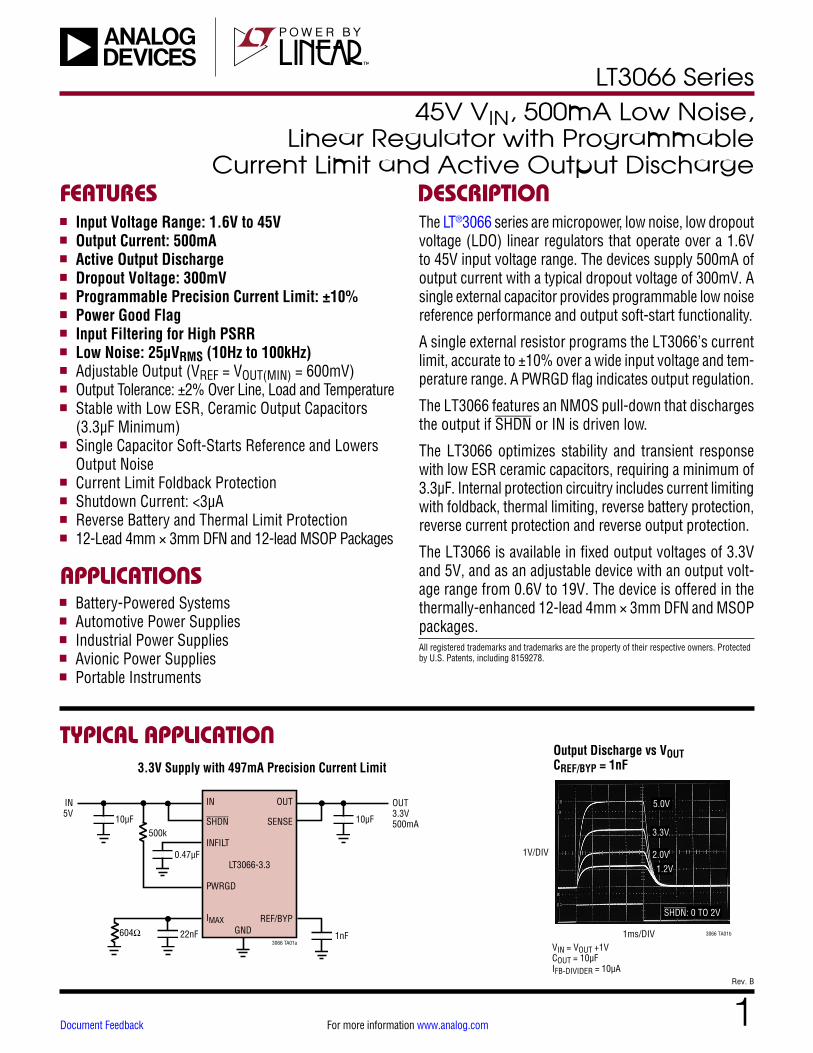
LT3066 Series
1Rev. B
For more information www.analog.comDocument Feedback
TYPICAL APPLICATION
FEATURES DESCRIPTION
45V VIN, 500mA Low Noise, Linear Regulator with Programmable
Current Limit and Active Output Discharge
The LT®3066 series are micropower, low noise, low dropout voltage (LDO) linear regulators that operate over a 1.6V to 45V input voltage range. The devices supply 500mA of output current with a typical dropout voltage of 300mV. A single external capacitor provides programmable low noise reference performance and output soft-start functionality.
A single external resistor programs the LT3066’s current limit, accurate to ±10% over a wide input voltage and tem-perature range. A PWRGD flag indicates output regulation.
The LT3066 features an NMOS pull-down that discharges the output if SHDN or IN is driven low.
The LT3066 optimizes stability and transient response with low ESR ceramic capacitors, requiring a minimum of 3.3µF. Internal protection circuitry includes current limiting with foldback, thermal limiting, reverse battery protection, reverse current protection and reverse output protection.
The LT3066 is available in fixed output voltages of 3.3V and 5V, and as an adjustable device with an output volt-age range from 0.6V to 19V. The device is offered in the thermally-enhanced 12-lead 4mm × 3mm DFN and MSOP packages.
3.3V Supply with 497mA Precision Current Limit
APPLICATIONS
n Input Voltage Range: 1.6V to 45V n Output Current: 500mA n Active Output Discharge n Dropout Voltage: 300mV n Programmable Precision Current Limit: ±10% n Power Good Flag n Input Filtering for High PSRR n Low Noise: 25µVRMS (10Hz to 100kHz) n Adjustable Output (VREF = VOUT(MIN) = 600mV) n Output Tolerance: ±2% Over Line, Load and Temperature n Stable with Low ESR, Ceramic Output Capacitors
(3.3µF Minimum) n Single Capacitor Soft-Starts Reference and Lowers
Output Noise n Current Limit Foldback Protection n Shutdown Current: <3µA n Reverse Battery and Thermal Limit Protection n 12-Lead 4mm × 3mm DFN and 12-lead MSOP Packages
n Battery-Powered Systems n Automotive Power Supplies n Industrial Power Supplies n Avionic Power Supplies n Portable Instruments
All registered trademarks and trademarks are the property of their respective owners. Protected by U.S. Patents, including 8159278.
Output Discharge vs VOUT CREF/BYP = 1nF
3066 TA01b1ms/DIV
1V/DIV 2.0V
3.3V
1.2V
VIN = VOUT +1VCOUT = 10µFIFB-DIVIDER = 10µA
SHDN: 0 TO 2V
5.0V
LT3066-3.3
GND
IN OUT
SENSE
REF/BYP
INFILT
SHDN
PWRGD
IMAX
10µF
IN5V
OUT3.3V500mA10µF
604Ω 22nF
0.47µF
3066 TA01a1nF
500k
LT3066 Series
2Rev. B
For more information www.analog.com
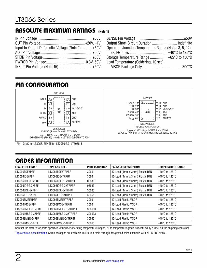
ABSOLUTE MAXIMUM RATINGSIN Pin Voltage .........................................................±50VOUT Pin Voltage .............................................. +20V, –1VInput-to-Output Differential Voltage (Note 2) ............ ±50VADJ Pin Voltage ......................................................±50V SHDN Pin Voltage ...................................................±50VPWRGD Pin Voltage .......................................–0.3V, 50VINFILT Pin Voltage (Note 15) ...................................±50V
(Note 1)
ORDER INFORMATIONLEAD FREE FINISH TAPE AND REEL PART MARKING* PACKAGE DESCRIPTION TEMPERATURE RANGE
LT3066EDE#PBF LT3066EDE#TRPBF 3066 12-Lead (4mm x 3mm) Plastic DFN –40°C to 125°CLT3066IDE#PBF LT3066IDE#TRPBF 3066 12-Lead (4mm x 3mm) Plastic DFN –40°C to 125°CLT3066EDE-3.3#PBF LT3066EDE-3.3#TRPBF 06633 12-Lead (4mm x 3mm) Plastic DFN –40°C to 125°CLT3066IDE-3.3#PBF LT3066IDE-3.3#TRPBF 06633 12-Lead (4mm x 3mm) Plastic DFN –40°C to 125°CLT3066EDE-5#PBF LT3066EDE-5#TRPBF 30665 12-Lead (4mm x 3mm) Plastic DFN –40°C to 125°CLT3066IDE-5#PBF LT3066IDE-5#TRPBF 30665 12-Lead (4mm x 3mm) Plastic DFN –40°C to 125°CLT3066EMSE#PBF LT3066EMSE#TRPBF 3066 12-Lead Plastic MSOP –40°C to 125°CLT3066IMSE#PBF LT3066IMSE#TRPBF 3066 12-Lead Plastic MSOP –40°C to 125°CLT3066EMSE-3.3#PBF LT3066EMSE-3.3#TRPBF 306633 12-Lead Plastic MSOP –40°C to 125°C
LT3066IMSE-3.3#PBF LT3066IMSE-3.3#TRPBF 306633 12-Lead Plastic MSOP –40°C to 125°C
LT3066EMSE-5#PBF LT3066EMSE-5#TRPBF 30665 12-Lead Plastic MSOP –40°C to 125°CLT3066IMSE-5#PBF LT3066IMSE-5#TRPBF 30665 12-Lead Plastic MSOP –40°C to 125°C
Contact the factory for parts specified with wider operating temperature ranges. *The temperature grade is identified by a label on the shipping container.
Tape and reel specifications. Some packages are available in 500 unit reels through designated sales channels with #TRMPBF suffix.
12
11
10
9
8
7
13GND
1
2
3
4
5
6
OUT
OUT
NC/SENSE*
ADJ
GND
REF/BYP
INFILT
IN
IN
SHDN
PWRGD
IMAX
TOP VIEW
DE PACKAGE12-LEAD (4mm × 3mm) PLASTIC DFN
TJMAX = 150°C, θJA = 34°C/W, θJC = 5°C/WEXPOSED PAD (PIN 13) IS GND, MUST BE SOLDERED TO PCB
123456
INFILTININ
SHDNPWRGD
IMAX
121110987
OUTOUTNC/SENSE*ADJGNDREF/BYP
TOP VIEW
13GND
MSE PACKAGE12-LEAD PLASTIC MSOP
TJMAX = 150°C, θJA = 34°C/W, θJC = 6°C/WEXPOSED PAD (PIN 13) IS GND, MUST BE SOLDERED TO PCB
*Pin 10: NC for LT3066, SENSE for LT3066-3.3, LT3066-5
PIN CONFIGURATION
SENSE Pin Voltage ..................................................±50VOutput Short-Circuit Duration .......................... IndefiniteOperating Junction Temperature Range (Notes 3, 5, 14) E-, I-Grades ....................................... –40°C to 125°CStorage Temperature Range .................. –65°C to 150°CLead Temperature (Soldering, 10 sec) MSOP Package Only ......................................... 300°C
LT3066 Series
3Rev. B
For more information www.analog.com
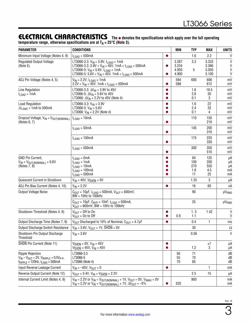
ELECTRICAL CHARACTERISTICS The l denotes the specifications which apply over the full operating temperature range, otherwise specifications are at TA = 25°C (Note 3).
PARAMETER CONDITIONS MIN TYP MAX UNITS
Minimum Input Voltage (Notes 4, 9) ILOAD = 500mA l 1.6 2.2 V
Regulated Output Voltage (Note 5)
LT3066-3.3: VIN = 3.9V, ILOAD = 1mA LT3066-3.3: 3.9V < VIN < 45V, 1mA < ILOAD < 500mA LT3066-5: VIN = 5.6V, ILOAD = 1mA LT3066-5: 5.6V < VIN < 45V, 1mA < ILOAD < 500mA
l
l
3.267 3.234 4.950 4.900
3.3 5
3.333 3.366 5.050 5.100
V V V V
ADJ Pin Voltage (Notes 4, 5) VIN = 2.2V, ILOAD = 1mA 2.2V < VIN < 45V, 1mA < ILOAD < 500mA
l
594 588
600 606 612
mV mV
Line Regulation ILOAD = 1mA
LT3066-3.3: ΔVIN = 3.9V to 45V LT3066-5: ΔVIN = 5.6V to 45V LT3066: ΔVIN = 2.2V to 45V (Note 4)
l
l
l
1.6 2.6 0.1
19.5 30 3
mV mV mV
Load Regulation ΔILOAD = 1mA to 500mA
LT3066-3.3: VIN = 3.9V LT3066-5: VIN = 5.6V LT3066: VIN = 2.2V (Note 4)
l
l
l
1.6 2.4 0.1
22 33 4
mV mV mV
Dropout Voltage, VIN = VOUT(NOMINAL) (Notes 6, 7)
ILOAD = 10mA
l
110 150 210
mV mV
ILOAD = 50mA
l
145 200 310
mV mV
ILOAD = 100mA
l
175 220 330
mV mV
ILOAD = 500mA
l
300 350 510
mV mV
GND Pin Current, VIN = VOUT(NOMINAL) + 0.6V (Notes 7, 8)
ILOAD = 0mA ILOAD = 1mA ILOAD = 10mA ILOAD = 100mA ILOAD = 500mA
l
l
l
l
l
64 100 270 1.8 11
125 200 550 4.5 25
µA µA µA
mA mA
Quiescent Current in Shutdown VIN = 45V, VSHDN = 0V 1.25 3 µA
ADJ Pin Bias Current (Notes 4, 10) VIN = 2.2V l 16 60 nA
Output Voltage Noise COUT = 10µF, ILOAD = 500mA, VOUT = 600mV, BW = 10Hz to 100kHz
90 µVRMS
COUT = 10µF, CBYP = 10nF, ILOAD = 500mA, VOUT = 600mV, BW = 10Hz to 100kHz
25 µVRMS
Shutdown Threshold (Notes 4, 9) VOUT = Off to On VOUT = On to Off
l
l
0.9
1. 3 1.1
1.42 V V
Output Discharge Time (Notes 7, 9) VOUT Discharged to 10% of Nominal, COUT = 4.7μF l 0.4 1 ms
Output Discharge Switch Resistance VIN = 3.6V, VOUT = 1V, SHDN = 0V 30 Ω
Shutdown Pin Output Discharge Threshold
VIN = 3.6V 0.56 V
SHDN Pin Current (Note 11) VSHDN = 0V, VIN = 45V VSHDN = 45V, VIN = 45V
l
l
1.2
±1 3
µA µA
Ripple Rejection VIN – VOUT = 2V, VRIPPLE = 0.5VP-P, fRIPPLE = 120Hz, ILOAD = 500mA
LT3066-3.3 LT3066-5 LT3066 (Note 4)
56 55 70
71 70 85
dB dB dB
Input Reverse Leakage Current VIN = –45V, VOUT = 0 l 1 mA
Reverse Output Current (Note 12) VOUT = 3.4V, VIN = VSHDN = 2.2V 2.5 15 µA
Internal Current Limit (Notes 4, 9) VIN = 2.2V or VIN = VOUT(NOMINAL) + 1V, VOUT = 0V, VIMAX = 0V VIN = 2.2V or VIN = VOUT(NOMINAL) + 1V, ΔVOUT = –5%
l
520
900 mA mA
LT3066 Series
4Rev. B
For more information www.analog.com
PARAMETER CONDITIONS MIN TYP MAX UNITS
External Programmed Current Limit (Notes 7, 13)
RIMAX = 1.5k, VOUT = 95% of VOUT(NOMINAL) VOUT(NOMINAL) + 0.6V < VIN < VOUT(NOMINAL)+ 5V RIMAX = 604Ω, VOUT = 95% of VOUT(NOMINAL) VOUT(NOMINAL) + 0.6V < VIN < VOUT(NOMINAL) + 2V
l
l
180
445
200
495
220
545
mA
mA
PWRGD Logic Low Voltage Pull-Up Current = 50µA l 0.07 0.25 V
PWRGD Leakage Current VPWRGD = 5V 0.01 1 µA
PWRGD Trip Point % of Nominal Output Voltage, Output Rising l 86 90 94 %
PWRGD Trip Point Hysteresis % of Nominal Output Voltage 1.6 %
ELECTRICAL CHARACTERISTICS The l denotes the specifications which apply over the full operating temperature range, otherwise specifications are at TA = 25°C (Note 3).
Note 1: Stresses beyond those listed under Absolute Maximum Ratings may cause permanent damage to the device. Exposure to any Absolute Maximum Rating condition for extended periods may affect device reliability and lifetime.Note 2: Absolute maximum input-to-output differential voltage is not achievable with all combinations of rated IN pin and OUT pin voltages. With IN at 50V, do not pull OUT below 0V. If OUT is pulled above IN and GND, the OUT to IN differential voltage must not exceed 40V.Note 3: The LT3066 regulator is tested and specified under pulse load conditions such that TJ ≅ TA. The LT3066E regulators are 100% tested at TA = 25°C and performance is guaranteed from 0°C to 125°C. Performance at –40°C to 125°C is assured by design, characterization and correlation with statistical process controls. The LT3066I regulators are guaranteed over the full –40°C to 125°C operating junction temperature range. High junction temperatures degrade operating lifetimes. Operating lifetime is derated at junction temperatures greater than 125°C.Note 4: The LT3066 adjustable version is tested and specified for these conditions with the ADJ pin connected to the OUT pin.Note 5: Maximum junction temperature limits operating conditions. Regulated output voltage specifications do not apply for all possible combinations of input voltage and output current. If operating at the maximum input voltage, limit the output current range. If operating at the maximum output current, limit the input voltage range. Current limit foldback limits the maximum output current as a function of input-to-output voltage. See Current Limit vs VIN – VOUT in the Typical Performance Characteristics section.Note 6: Dropout voltage is the minimum IN-to-OUT differential voltage needed to maintain regulation at a specified output current. In dropout, the output voltage equals (VIN – VDROPOUT). For some output voltages, minimum input voltage requirements limit dropout voltage.
Note 7: To satisfy minimum input voltage requirements, the LT3066 adjustable version is tested and specified for these conditions with an external resistor divider (60.4k bottom, 442k top) which sets VOUT to 5V. The divider adds 10uA of output DC load. This external current is not factored into GND pin current. For fixed voltage options, an internal resistor divider will add 5μA to the GND pin current. See the GND Pin Current curves in the Typical Performance Characteristics sectionNote 8: GND pin current is tested with VIN = VOUT(NOMINAL) + 0.6V and a current source load. GND pin current increases in dropout. See GND pin current curves in the Typical Performance Characteristics section.Note 9: To satisfy requirements for minimum input voltage, the LT3066 is tested at VIN = VOUT(NOMINAL) + 1V or VIN = 2.2V, whichever is greater.Note 10: ADJ pin bias current flows out of the ADJ pin.Note 11: SHDN pin current flows into the SHDN pin.Note 12: This current flows into the OUT pin and out of the GND pin.Note 13: Current limit varies inversely with the external resistor value tied from the IMAX pin to GND. If the externally programmed current limit feature is unused, tie the IMAX pin to GND. The internal current limit circuitry implements short-circuit protection as specified. Note 14: This IC includes over temperature protection that protects the device during overload conditions. Junction temperature exceeds 125°C (LT3066E, LT3066I) when the over temperature circuitry is active. Continuous operation above the specified maximum junction temperature may impair device reliability. Note 15: Tie INFILT directly to IN or to a decoupling capacitor.
LT3066 Series
5Rev. B
For more information www.analog.com
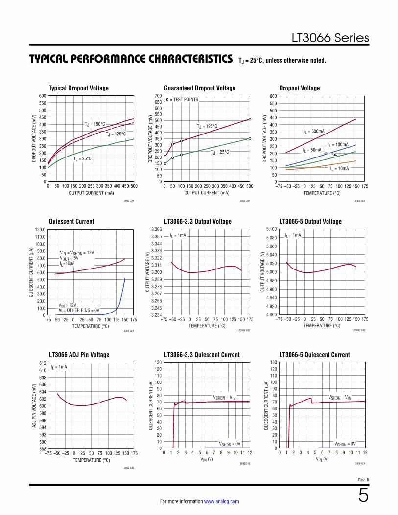
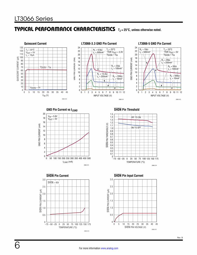
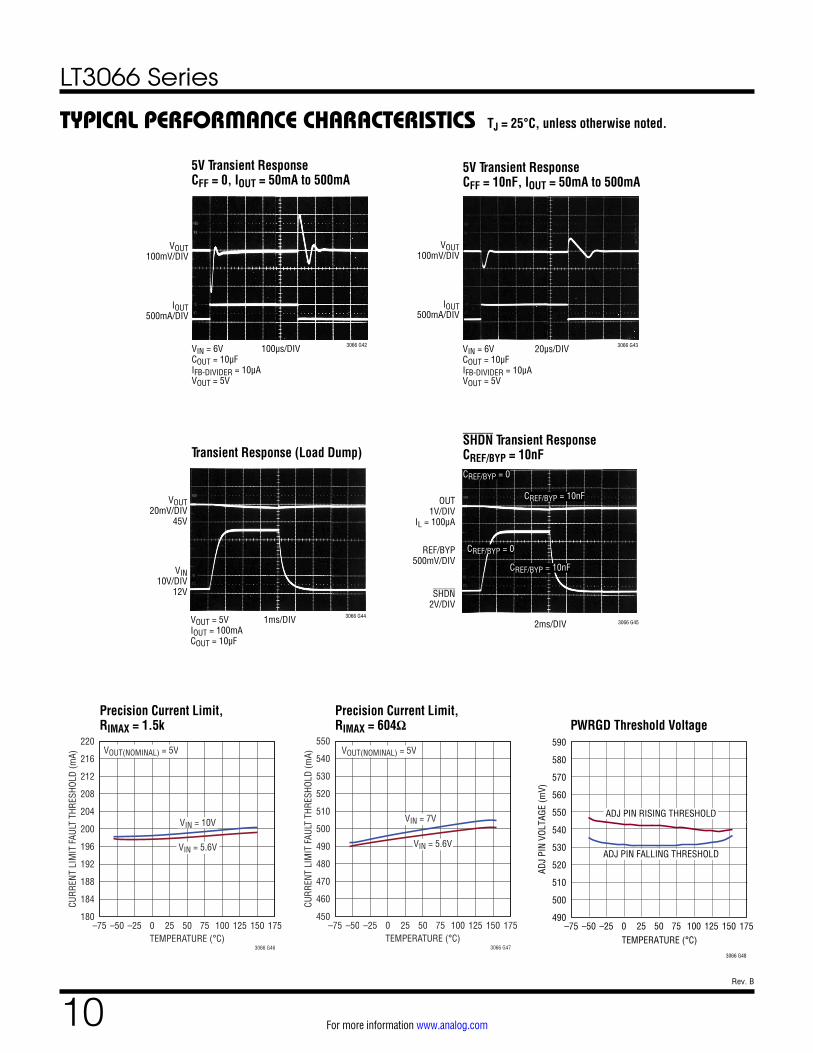
TYPICAL PERFORMANCE CHARACTERISTICS
Quiescent Current
LT3066 ADJ Pin Voltage
Typical Dropout Voltage Guaranteed Dropout Voltage
LT3066-3.3 Output Voltage
LT3066-3.3 Quiescent Current
Dropout Voltage
LT3066-5 Output Voltage
LT3066-5 Quiescent Current
OUTPUT CURRENT (mA)0
DROP
OUT
VOLT
AGE
(mV)
300
400
500
600
400
3066 G01
200
100
250
350
450
550
150
50
0100 200 30050 450150 250 350 500
TJ = 25°C
TJ = 125°C
TJ = 150°C
OUTPUT CURRENT (mA)0
0
DROP
OUT
VOLT
AGE
(mV)
100
200
300
700
500
100 200 250 450
600
400
50
150
250
650
450
550
350
50 150 300 350 400 500
3066 G02
TJ = 25°C
TJ = 125°C
= TEST POINTS
TEMPERATURE (°C)–75
DROP
OUT
VOLT
AGE
(mV)
300
400
500
600
125
3066 G03
200
100
250
350
450
550
150
50
0–25 25 75–50 1500 50 100 175
IL = 10mA
IL = 100mA
IL = 500mA
IL = 50mA
TJ = 25°C, unless otherwise noted.
IL = 1mA
TEMPERATURE (°C)–75 –50 –25 0 25 50 75 100 125 150 175
3.234
3.245
3.256
3.267
3.278
3.289
3.300
3.311
3.322
3.333
3.344
3.355
3.366
OUTP
UT V
OLTA
GE (V
)
LT3066 G05
TEMPERATURE (°C)–75
ADJ
PIN
VOLT
AGE
(mV)
600
604
608
612
125
3066 G07
596
592
598
602
606
610
594
590
588–25 25 75–50 1500 50 100 175
IL = 1mA
VSHDN = VIN
VSHDN = 0V
VIN (V)0 1 2 3 4 5 6 7 8 9 10 11 12
0102030405060708090
100110120130
QUIE
SCEN
T CU
RREN
T (µ
A)
3066 G08
VSHDN = VIN
VSHDN = 0V
VIN (V)0 1 2 3 4 5 6 7 8 9 10 11 12
0102030405060708090
100110120130
QUIE
SCEN
T CU
RREN
T (µ
A)
3066 G09
VIN = VSHDN = 12VVOUT = 5VIL=10µA
VIN = 12VALL OTHER PINS = 0V
TEMPERATURE (°C)–75 –50 –25 0 25 50 75 100 125 150 175
0
10.0
20.0
30.0
40.0
50.0
60.0
70.0
80.0
90.0
100.0
110.0
120.0
QUIE
SCEN
T CU
RREN
T (µ
A)
Quiescent Current
3066 G04
IL = 1mA
TEMPERATURE (°C)–75 –50 –25 0 25 50 75 100 125 150 175
4.900
4.920
4.940
4.960
4.980
5.000
5.020
5.040
5.060
5.080
5.100
OUTP
UT V
OLTA
GE (V
)
LT3066 G06
LT3066 Series
6Rev. B
For more information www.analog.com
TYPICAL PERFORMANCE CHARACTERISTICS TJ = 25°C, unless otherwise noted.
SHDN Pin Current
SHDN Pin Threshold
TJ = 25°CVOUT = 5VIL = 10µA
VIN (V)0 5 10 15 20 25 30 35 40 45
0102030405060708090
100110120130
QUIE
SCEN
T CU
RREN
T (µ
A)
Quiescent Current
3066 G10
VSHDN = 0V
VSHDN = VIN
SHDN Pin Input Current
ILOAD (mA)0
GND
PIN
CURR
ENT
(mA)
12
16
20
400
3066 G13
8
4
10
14
18
6
2
0100 200 30050 450150 250 350 500
VIN = 5.6VVOUT = 5V
TEMPERATURE (°C)–75
SHDN
PIN
THR
ESHO
LD (V
)
1.0
1.2
1.41.5
1.3
1.1
0.9
25 50 100 175
0.6
0.8
0.2
0.40.5
0.7
0.1
0.3
0–50 –25 0 75 125 150
3066 G14
OFF TO ON
ON TO OFF
INPUT VOLTAGE (V)0
GND
PIN
CURR
ENT
(mA) 18
20
8
3066 G11
12
1614
22
24
10
8
64
2
02 4 61 93 5 7 121110
TJ = 25°C*FOR VOUT = 3.3VVSHDN = VIN
RL = 6.6ΩIL = 500mA*
RL = 13.2ΩIL = 250mA*
RL = 33ΩIL = 100mA*
RL = 330ΩIL = 10mA*
INPUT VOLTAGE (V)0
GND
PIN
CURR
ENT
(mA) 18
20
8
3066 G12
12
1614
22
24
10
8
64
2
02 4 61 93 5 7 121110
TJ = 25°C*FOR VOUT = 5VVSHDN = VIN
RL = 10ΩIL = 500mA*
RL = 20ΩIL = 250mA*
RL = 50ΩIL = 100mA*
RL = 500ΩIL = 10mA*
SHDN = 45V
TEMPERATURE (°C)–75 –50 –25 0 25 50 75 100 125 150 175
0
0.5
1.0
1.5
2.0
2.5
3.0
SHDN
PIN
CUR
RENT
(µA)
SHDN Pin Current
3066 G15
SHDN PIN VOLTAGE (V)0 5 10 15 20 25 30 35 40 45
0
0.5
1.0
1.5
2.0
2.5
3.0
SHDN
PIN
CUR
RENT
(µA)
SHDN Pin Input Current
3066 G16
Quiescent Current LT3066-3.3 GND Pin Current LT3066-5 GND Pin Current
GND Pin Current vs ILOAD
LT3066 Series
7Rev. B
For more information www.analog.com
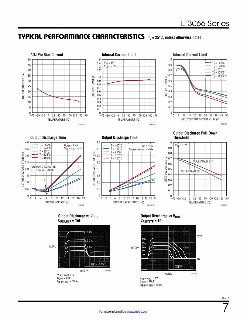
ADJ Pin Bias Current Internal Current Limit Internal Current Limit
Output Discharge Time Output Discharge TimeOutput Discharge Pull-Down Threshold
TYPICAL PERFORMANCE CHARACTERISTICS
Output Discharge vs VOUT CREF/BYP = 1nF
TJ = 25°C, unless otherwise noted.
Output Discharge vs VOUT CREF/BYP = 1nF
TEMPERATURE (°C)–75
ADJ
PIN
CURR
ENT
(nA)
30
40
50
125
3066 G17
20
10
25
35
45
15
5
0–25 25 75–50 1500 50 100 175
TEMPERATURE (°C)–75
CURR
ENT
LIM
IT (A
)
1.0
1.2
1.41.5
1.3
1.1
0.9
25 50 100 175
0.6
0.8
0.2
0.40.5
0.7
0.1
0.3
0–50 –25 0 75 125 150
3066 G18
VIN = 6VVOUT = 0V
COUT = 4.7µFVIN = VOUT + 1V
OUTPUT DISCHARGE FOLDBACK STARTS
T = –55°CT = –40°CT = 25°CT = 125°CT = 150°C
OUTPUT VOLTAGE (V)0 2 4 6 8 10 12 14 16 18 20
0
0.5
1.0
1.5
2.0
2.5
3.0
3.5
4.0
OUTP
UT D
ISCH
ARGE
TIM
E (m
s)
3066 G20
TJ = –55°CTJ = –40°CTJ = 25°CTJ = 125°CTJ = 150°C
INPUT/OUTPUT DIFFERENTIAL (V)0 5 10 15 20 25 30 35 40 45 50
0
0.1
0.2
0.3
0.4
0.5
0.6
0.7
0.8
0.9
1.0
CURR
ENT
LIM
IT (A
)
Internal Current Limit
3066 G19
VIN = 4.3VVOUT(NOMINAL) = 3.3V
T = –55°CT = –40°CT = 25°CT = 125°CT = 155°C
OUTPUT CAPACITANCE (µF)0 2 4 6 8 10 12 14 16 18 20 22 24
0
0.5
1.0
1.5
2.0
2.5
3.0
3.5
4.0
OUTP
UT D
ISCH
ARGE
TIM
E (m
s)
Output Discharge Time
LT3066 G21
PULL-DOWN ON
PULL-DOWN OFF
VIN = 3.6V
TEMPERATURE (°C)–75 –50 –25 0 25 50 75 100 125 150 175
0
0.1
0.2
0.3
0.4
0.5
0.6
0.7
0.8
0.9
1.0
SHDN
PIN
VOL
TAGE
(V)
Pulldown Threshold
3066 G22
3066 G231ms/DIV
1V/DIV
5.0V
2.0V
3.3V
1.2V
VIN = VOUT +1VCOUT = 10µFIFB-DIVIDER = 10µA
SHDN: 0 TO 2V
3066 G241ms/DIV
5V/DIV
20V19V
12V15V
8V5V
0V
VIN = VOUT +1VCOUT = 10µFIFB-DIVIDER = 10µA
SHDN: 0 TO 2V
LT3066 Series
8Rev. B
For more information www.analog.com
TYPICAL PERFORMANCE CHARACTERISTICS TJ = 25°C, unless otherwise noted.
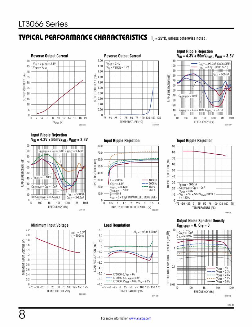
Output Noise Spectral Density CREF/BYP = 0, CFF = 0Load Regulation
IOUT = 500mACOUT = 3•3.3µFNo CREF/BYP, CFF, CINFILT
CREF/BYP = 10nF
CREF/BYP = CFF = 10nF
CREF/BYP = CFF = 10nF, CINFILT = 0.47µF
FREQUENCY (Hz)10 100 1k 10k 100k 1M 10M
0
10
20
30
40
50
60
70
80
90
100
RIPP
LE R
EJEC
TION
(dB)
IN RMS OUT
3066 G28INPUT/OUTPUT DIFFERENTIAL (V)
0 0.5 1 1.5 2 2.5 3 3.5 40
10.0
20.0
30.0
40.0
50.0
60.0
70.0
80.0
RIPP
LE R
EJEC
TION
(dB)
Input Ripple Rejection
3066 G29
IL = 500mA
COUT= 3 • 3.3µF IN PARALLEL (0805 SIZE)
CREF/BYP = 10nFCFF =10nF
VOUT = 3.3VCINFILT = 0.47µF
100kHz500kHz1MHz2MHz
TEMPERATURE (°C)–75
0
RIPP
LE R
EJEC
TION
(dB)
10
30
40
50
75 100 125 150
90
3066 G30
20
–50 –25 0 25 50 175
60
70
80
ILOAD = 500mACREF/BYP = CFF = 10nFVOUT = 3.3VVIN = 4.3V + 50mVRMS RIPPLEf = 120Hz
TEMPERATURE (°C)–75 –50 –25 0 25 50 75 100 125 150 175
0
0.2
0.4
0.6
0.8
1.0
1.2
1.4
1.6
1.8
2.0
2.2
MIN
IMUM
INPU
T VO
LTAG
E (V
)
3066 G31
VOUT = 0.6VIL = 500mA
∆IL = 1mA to 500mA
TEMPERATURE (°C)–75 –50 –25 0 25 50 75 100 125 150 175
–7.0
–6.0
–5.0
–4.0
–3.0
–2.0
–1.0
0
1.0
2.0
3.0
LOAD
REG
ULAT
ION
(mV)
3066 G32
LT3066-5, VIN = 6VLT3066-3.3, VIN = 4.3VLT3066, VOUT = 0.6V, VIN = 2.2V
FREQUENCY (Hz)
0.1
OUTP
UT N
OISE
SPE
CTRA
L DE
NSIT
Y (µ
V/√H
z)
1
10 1k 10k 100k
3066 G33
0.01100
10
VOUT = 5VVOUT = 3.3VVOUT = 2.5VVOUT = 1.2VVOUT = 0.6V
COUT = 10µFIL = 500mA
Input Ripple Rejection VIN = 4.3V + 50mVRMS, VOUT = 3.3V Input Ripple RejectionInput Ripple Rejection
Minimum Input Voltage
Input Ripple Rejection VIN = 4.3V + 50mVRMS, VOUT = 3.3VReverse Output Current Reverse Output Current
VOUT = 3.4VVIN = VSHDN = 2.2V
TEMPERATURE (°C)–75 –50 –25 0 25 50 75 100 125 150 175
0
0.20
0.40
0.60
0.80
1.00
1.20
1.40
1.60
1.80
2.00
OUTP
UT C
URRE
NT (m
A)
Reverse Output Current
3066 G26
IOUT = 500mA
CREF/BYP = 10nF
CREF/BYP = CFF = 10nF, CINFILT = 0.47µF
COUT = 3•3.3µF (0805 SIZE)COUT = 3.3µF (0805 SIZE)
FREQUENCY (Hz)10 100 1k 10k 100k 1M 10M
0
10
20
30
40
50
60
70
80
90
100
110
RIPP
LE R
EJEC
TION
(dB)
IN RMS OUT
3066 G27
VIN = VSHDN = 2.1VVADJ = VOUT
VOUT (V)0 2 4 6 8 10 12 14 16 18 20
0
5
10
15
20
25
30
35
40
45
50
OUTP
UT C
URRE
NT (µ
A)
Reverse Current
3066 G25
LT3066 Series
9Rev. B
For more information www.analog.com
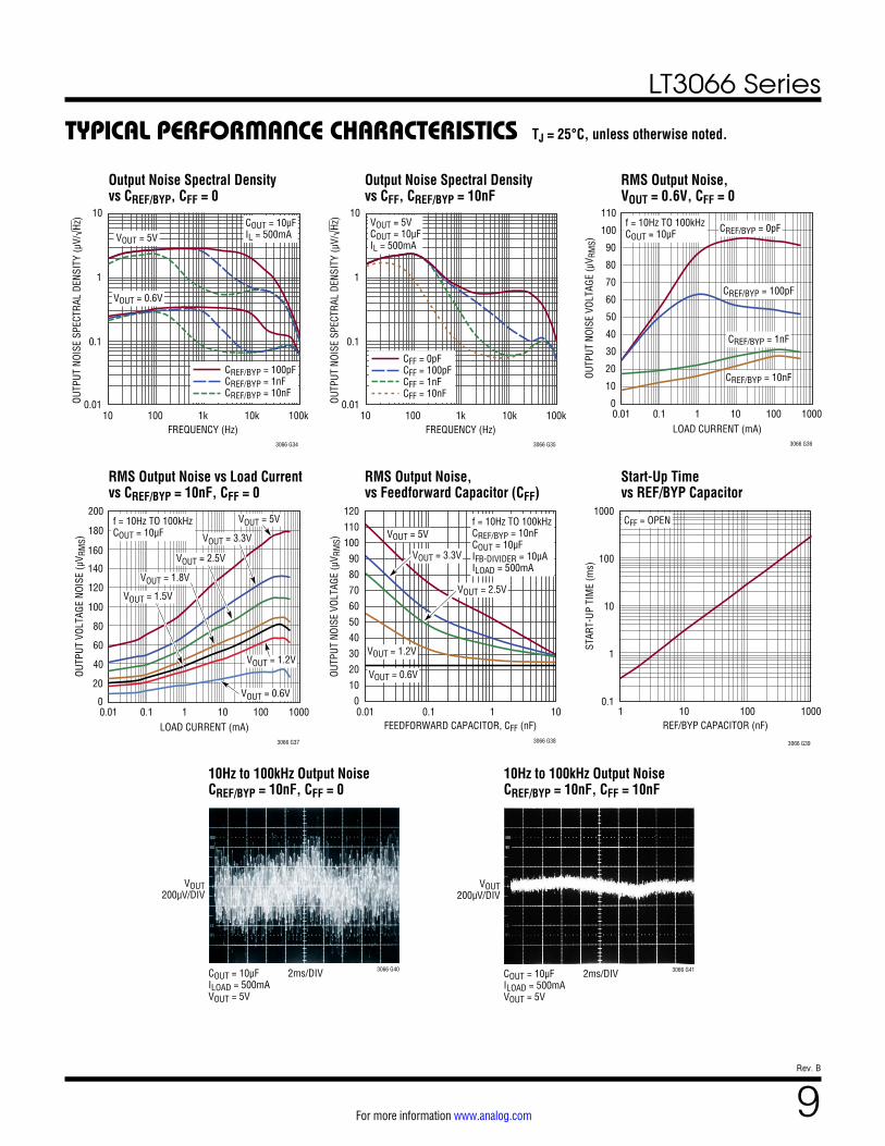
Output Noise Spectral Density vs CREF/BYP, CFF = 0
Output Noise Spectral Density vs CFF, CREF/BYP = 10nF
RMS Output Noise, vs Feedforward Capacitor (CFF)
Start-Up Time vs REF/BYP Capacitor
RMS Output Noise vs Load Current vs CREF/BYP = 10nF, CFF = 0
RMS Output Noise, VOUT = 0.6V, CFF = 0
10Hz to 100kHz Output Noise CREF/BYP = 10nF, CFF = 0
10Hz to 100kHz Output Noise CREF/BYP = 10nF, CFF = 10nF
TYPICAL PERFORMANCE CHARACTERISTICS TJ = 25°C, unless otherwise noted.
FREQUENCY (Hz)
0.1
OUTP
UT N
OISE
SPE
CTRA
L DE
NSIT
Y (µ
V/√H
z)
1
10 1k 10k 100k
3066 G34
0.01100
10
VOUT = 5V
VOUT = 0.6V
COUT = 10µFIL = 500mA
CREF/BYP = 100pFCREF/BYP = 1nFCREF/BYP = 10nF
FREQUENCY (Hz)
0.1OU
TPUT
NOI
SE S
PECT
RAL
DENS
ITY
(µV/
√Hz)
1
10 1k 10k 100k
3066 G35
0.01100
10VOUT = 5VCOUT = 10µFIL = 500mA
CFF = 0pFCFF = 100pFCFF = 1nFCFF = 10nF
LOAD CURRENT (mA)0.01
40
OUTP
UT N
OISE
VOL
TAGE
(µV R
MS)
50
60
70
80
0.1 1 10 100 1000
3066 G36
30
20
10
0
90
110CREF/BYP = 0pF
CREF/BYP = 100pF
CREF/BYP = 1nF
CREF/BYP = 10nF
100f = 10Hz TO 100kHzCOUT = 10µF
LOAD CURRENT (mA)0.01
OUTP
UT V
OLTA
GE N
OISE
(µV R
MS)
120
140
160
0.1 1 10 100 1000
3066 G37
40
60
80
100
20
0
200
180VOUT = 5V
VOUT = 3.3V
VOUT = 1.8V
VOUT = 1.2V
VOUT = 1.5V
VOUT = 2.5V
VOUT = 0.6V
f = 10Hz TO 100kHzCOUT = 10µF
FEEDFORWARD CAPACITOR, CFF (nF)
20OUTP
UT N
OISE
VOL
TAGE
(µV R
MS)
40
60
80
100
0.01 1 10
3066 G38
00.1
120
10
30
50
70
90
110 f = 10Hz TO 100kHzCREF/BYP = 10nFCOUT = 10µFIFB-DIVIDER = 10µAILOAD = 500mA
VOUT = 5V
VOUT = 3.3V
VOUT = 2.5V
VOUT = 1.2V
VOUT = 0.6V
REF/BYP CAPACITOR (nF)
0.1
STAR
T-UP
TIM
E (m
s)
10
1000
1
100
100
3066 G39
1000101
CFF = OPEN
VOUT200µV/DIV
2ms/DIVCOUT = 10µFILOAD = 500mAVOUT = 5V
3066 G40
VOUT200µV/DIV
2ms/DIVCOUT = 10µFILOAD = 500mAVOUT = 5V
3066 G41
LT3066 Series
10Rev. B
For more information www.analog.com
TYPICAL PERFORMANCE CHARACTERISTICS TJ = 25°C, unless otherwise noted.
VOUT(NOMINAL) = 5V
VIN = 5.6V
VIN = 10V
TEMPERATURE (°C)–75 –50 –25 0 25 50 75 100 125 150 175
180
184
188
192
196
200
204
208
212
216
220
CURR
ENT
LIM
IT F
AULT
THR
ESHO
LD (m
A)
IMAX
3066 G46
VOUT(NOMINAL) = 5V
VIN = 5.6V
VIN = 7V
TEMPERATURE (°C)–75 –50 –25 0 25 50 75 100 125 150 175
450
460
470
480
490
500
510
520
530
540
550
CURR
ENT
LIM
IT F
AULT
THR
ESHO
LD (m
A)
IMAX
3066 G47TEMPERATURE (°C)
–75
ADJ
PIN
VOLT
AGE
(mV)
550
570
590
125
3066 G48
530
510
540
560
580
520
500
490–25 25 75–50 1500 50 100 175
ADJ PIN RISING THRESHOLD
ADJ PIN FALLING THRESHOLD
Precision Current Limit, RIMAX = 1.5k
Precision Current Limit, RIMAX = 604Ω PWRGD Threshold Voltage
Transient Response (Load Dump)SHDN Transient Response CREF/BYP = 10nF
VOUT20mV/DIV
45V
VIN10V/DIV
12V
1ms/DIVVOUT = 5VIOUT = 100mACOUT = 10µF
3066 G44
OUT1V/DIV
IL = 100μA
REF/BYP500mV/DIV
SHDN2V/DIV
2ms/DIV 3066 G45
CREF/BYP = 0
CREF/BYP = 10nF
CREF/BYP = 10nF
CREF/BYP = 0
5V Transient Response CFF = 0, IOUT = 50mA to 500mA
5V Transient Response CFF = 10nF, IOUT = 50mA to 500mA
VOUT100mV/DIV
IOUT500mA/DIV
100µs/DIVVIN = 6VCOUT = 10µFIFB-DIVIDER = 10µAVOUT = 5V
3066 G42
VOUT100mV/DIV
IOUT500mA/DIV
20µs/DIVVIN = 6VCOUT = 10µFIFB-DIVIDER = 10µAVOUT = 5V
3066 G43
LT3066 Series
11Rev. B
For more information www.analog.com
INFILT (Pin 1): Filtered Input. This pin is connected to IN through a ~140Ω on-chip resistor. To improve PSRR, at frequencies greater than 10kHz connect up to a 0.47μF capacitor from INFILT to GND (see Figure 1). If improved PSRR is not needed, connect the INFILT pin to IN.
IN (Pins 2, 3): Input. These pin(s) supply power to the device. The LT3066 requires a local IN bypass capacitor if it is located more than six inches from the main input filter capacitor. In general, battery output impedance rises with frequency, so adding a bypass capacitor in battery-powered circuits is advisable. An input bypass capacitor in the range of 1µF to 10µF generally suffices. See Input Capacitance and Stability in the Applications Information section for more information.
The LT3066 withstands reverse voltages on the IN pin with respect to its GND and OUT pins. In such case, such as a battery plugged in backwards, the LT3066 behaves as if a diode is in series with its input. No reverse current flows into the LT3066 and no reverse voltage appears at the load. The device protects itself and the load.
SHDN (Pin 4): Shutdown. Pulling the SHDN pin low puts the LT3066 into a low power state and turns the output off. Drive the SHDN pin with either logic or an open col-lector/drain with a pull-up resistor. The resistor supplies the pull-up current to the open collector/drain logic, nor-mally several microamperes, and the SHDN pin current, typically less than 2µA. If unused, connect the SHDN pin to IN. The LT3066 does not function if the SHDN pin is not connected.
PWRGD (Pin 5): Power Good. The PWRGD pin is an open-drain output that actively pulls low if the output is less than 90% of the nominal output value. The PWRGD pin is capable of sinking 50µA. There is no internal pull-up resistor; an external pull-up resistor must be used.
IMAX (Pin 6): Precision Current Limit Programming. This pin is the collector of a current mirror PNP that is 1/500th the size of the output power PNP. This pin is also the input
to the current limit amplifier. The current limit threshold is set by connecting a resistor between the IMAX pin and GND.
For detailed information on how to set the IMAX pin resis-tor value, see the Applications Information section. The IMAX pin requires a 22nF de-coupling capacitor to ground. If not used, tie IMAX to GND. Do not drive this pin with any active circuitry.
REF/BYP (Pin 7): Bypass/Soft-Start. Connecting a capaci-tor from this pin to GND bypasses the LT3066’s reference noise and soft-starts the reference. A 10nF bypass capaci-tor typically reduces output voltage noise to 25µVRMS in a 10Hz to 100kHz bandwidth. Soft-start time is directly proportional to the BYP capacitor value. If the LT3066 is placed in shutdown, BYP is actively pulled low by an internal device to reset soft-start. If low noise or soft-start performance is not required, this pin must be left float-ing (unconnected). Do not drive this pin with any active circuitry.
Because the REF/BYP pin is the reference input to the error amplifier, stray capacitance at this point should be minimized. Special attention should be given to any stray capacitances that can couple external signals onto the REF/BYP pin producing undesirable output transients or ripple. A minimum capacitance of 100pF from REF/BYP to GND is recommended.
GND (Pin 8, Exposed Pad Pin 13): Ground. The exposed pad of the DFN and MSOP packages is an electrical con-nection to GND. To ensure proper electrical and thermal performance, solder Pin 8 to the PCB GND and tie it directly to Pin 13. For the adjustable LT3066, connect the bottom of the external resistor divider that sets output voltage directly to GND (Pin 8)for optimum load regulation.
ADJ (Pin 9): Adjust. This pin is the error amplifier’s invert-ing terminal. It’s typical bias current of 16nA flows out of the pin (see curve of ADJ Pin Bias Current vs Temperature in the Typical Performance Characteristics section). The ADJ pin voltage is 600mV referenced to GND.
PIN FUNCTIONS (DFN/MSOP)
LT3066 Series
12Rev. B
For more information www.analog.com
PIN FUNCTIONS (DFN/MSOP)
NC (LT3066: Pin 10): No Connect. This pin has no con-nection to internal circuitry. This pin may be floated or connected to GND.
SENSE (LT3066-3.3, LT3066-5: Pin 10): Sense. This pin is the top of the internal resistor divider network and should be connected directly to the load, as a Kelvin sense, for optimum load regulation and transient per-formance. Connecting this pin to the output pin at the package, rather than directly to the load, can result in load regulation errors due to the current across the parasitic resistance of the PCB trace.
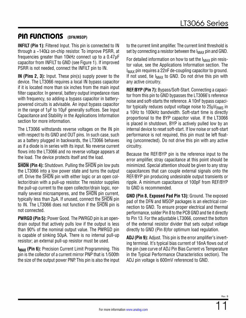
OUT (Pins 11, 12): Output. These pins supply power to the load. Stability requirements demand a minimum 3.3µF ceramic output capacitor with an ESR < 1Ω to prevent oscillations. Applications with output voltages less than 1.2V require a minimum 4.7µF ceramic output capaci-tor. Large load transient applications require larger out-put capacitors to limit peak voltage transients. See the Applications Information section for details on transient response and reverse output characteristics. Permissible output voltage range is 600mV to 19V.
Connecting a capacitor from OUT to ADJ reduces output noise and improves transient response for output voltages greater than 600mV. See the Applications Information sec-tion for calculating the value of the feedforward capacitor.
At output voltages above 0.6V, the resistor divider connected to the ADJ pin is used to regulate voltage at the load. Parasitic resistances of PCB traces or cables can therefore result in load regulation errors at high output currents. To eliminate these, connect the resistor divider directly to the load for a Kelvin sense connection, as shown in Figure 1.
If the LT3066 is placed in shutdown, OUT is actively discharged by an internal NMOS device. Gate drive is controlled to insure that a 10μF capacitor is discharged 90% in 2ms or less. If IN is driven low, OUT is actively discharged to ~800mV. For OUT voltages greater than 6V, current limit foldback is implemented to protect the NMOS device and discharge rates increase. See the Applications Information section for more information.
Figure 1. Kelvin Sense Connection
IN
SHDN
RPOUT
VINADJ
GND
LT3066
RP
R1
R2
++LOAD
3066 F01a
ADJUSTABLE VERSION
IN
SHDN
RPOUT
VINSENSE
GND
LT3066-X
RP
++LOAD
3066 F01b
FIXED VOLTAGE VERSION
LT3066 Series
13Rev. B
For more information www.analog.com
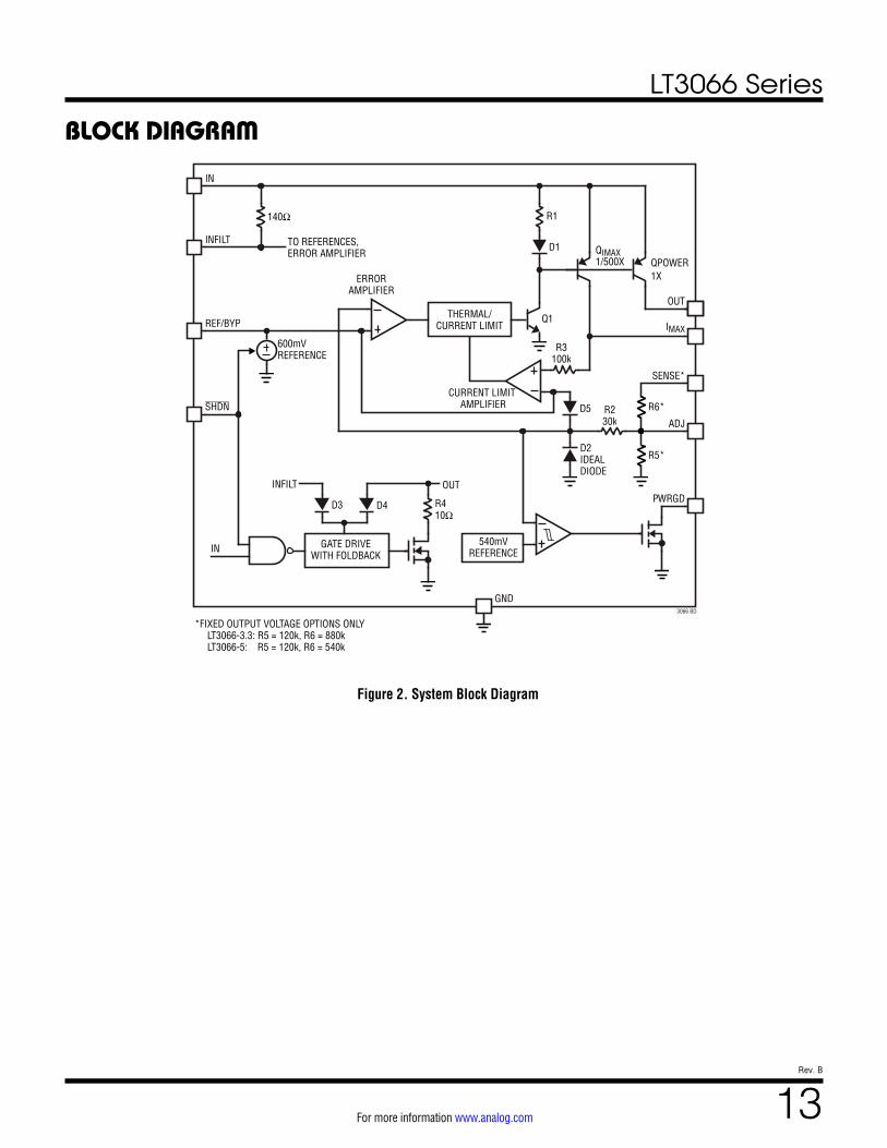
BLOCK DIAGRAM
Q1
1XQPOWER
QIMAX1/500X
D1
R1
D2IDEALDIODE
R230k
R3100k
D3 D4
140Ω
D5
R410Ω
IN
SHDN
THERMAL/CURRENT LIMIT
GND
IMAXREF/BYP
OUT
ADJ
600mVREFERENCE
540mVREFERENCE
PWRGD
GATE DRIVEWITH FOLDBACK
INFILT OUT
IN
INFILT
ERRORAMPLIFIER
CURRENT LIMIT AMPLIFIER
TO REFERENCES, ERROR AMPLIFIER
SENSE*
R5*
R6*
*FIXED OUTPUT VOLTAGE OPTIONS ONLY LT3066-3.3: R5 = 120k, R6 = 880k LT3066-5: R5 = 120k, R6 = 540k
3066 BD
Figure 2. System Block Diagram
LT3066 Series
14Rev. B
For more information www.analog.com
APPLICATIONS INFORMATION
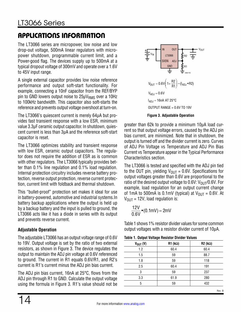
Figure 3. Adjustable Operation
VIN
VOUTIN OUT+LT3066
SHDN ADJ
GND
3066 F03
R2
R1
VOUT = 0.6V 1+R2R1
– IADJ •R2( )
VADJ = 0.6V
IADJ = 16nA AT 25°C
OUTPUT RANGE = 0.6V TO 19V
The LT3066 series are micropower, low noise and low drop-out voltage, 500mA linear regulators with micro-power shutdown, programmable current limit, and a Power-good flag. The devices supply up to 500mA at a typical dropout voltage of 300mV and operate over a 1.6V to 45V input range.
A single external capacitor provides low noise reference performance and output soft-start functionality. For example, connecting a 10nF capacitor from the REF/BYP pin to GND lowers output noise to 25μVRMS over a 10Hz to 100kHz bandwidth. This capacitor also soft-starts the reference and prevents output voltage overshoot at turn-on.
The LT3066’s quiescent current is merely 64μA but pro-vides fast transient response with a low ESR, minimum value 3.3μF ceramic output capacitor. In shutdown, quies-cent current is less than 3μA and the reference soft-start capacitor is reset.
The LT3066 optimizes stability and transient response with low ESR, ceramic output capacitors. The regula-tor does not require the addition of ESR as is common with other regulators. The LT3066 typically provides bet-ter than 0.1% line regulation and 0.1% load regulation. Internal protection circuitry includes reverse battery pro-tection, reverse output protection, reverse current protec-tion, current limit with foldback and thermal shutdown.
This “bullet-proof” protection set makes it ideal for use in battery-powered, automotive and industrial systems.In battery backup applications where the output is held up by a backup battery and the input is pulled to ground, the LT3066 acts like it has a diode in series with its output and prevents reverse current.
Adjustable Operation
The adjustable LT3066 has an output voltage range of 0.6V to 19V. Output voltage is set by the ratio of two external resistors, as shown in Figure 3. The device regulates the output to maintain the ADJ pin voltage at 0.6V referenced to ground. The current in R1 equals 0.6V/R1, and R2’s current is R1’s current minus the ADJ pin bias current.
The ADJ pin bias current, 16nA at 25°C, flows from the ADJ pin through R1 to GND. Calculate the output voltage using the formula in Figure 3. R1’s value should not be
greater than 62k to provide a minimum 10μA load cur-rent so that output voltage errors, caused by the ADJ pin bias current, are minimized. Note that in shutdown, the output is turned off and the divider current is zero. Curves of ADJ Pin Voltage vs Temperature and ADJ Pin Bias Current vs Temperature appear in the Typical Performance Characteristics section.
The LT3066 is tested and specified with the ADJ pin tied to the OUT pin, yielding VOUT = 0.6V. Specifications for output voltages greater than 0.6V are proportional to the ratio of the desired output voltage to 0.6V: VOUT/0.6V. For example, load regulation for an output current change of 1mA to 500mA is 0.1mV (typical) at VOUT = 0.6V. At VOUT = 12V, load regulation is:
12V0.6V
•(0.1mV) = 2mV
Table 1 shows 1% resistor divider values for some common output voltages with a resistor divider current of 10μA.
Table 1. Output Voltage Resistor Divider ValuesVOUT (V) R1 (kΩ) R2 (kΩ)
1.2 60.4 60.4
1.5 59 88.7
1.8 59 118
2.5 60.4 191
3 59 237
3.3 61.9 280
5 59 432
LT3066 Series
15Rev. B
For more information www.analog.com
APPLICATIONS INFORMATION
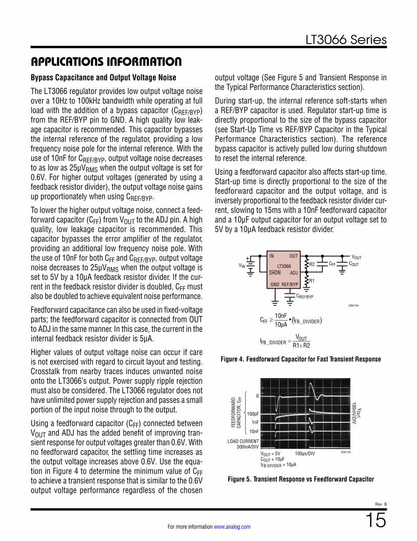
Figure 4. Feedforward Capacitor for Fast Transient Response
Figure 5. Transient Response vs Feedforward Capacitor
100µs/DIVVOUT = 5VCOUT = 10µFIFB-DIVIDER = 10µA
0
1nF
10nF
LOAD CURRENT500mA/DIV
FEED
FORW
ARD
CAPA
CITO
R, C
FF
100pF
3066 F05
VOUT
100mV/DIV
3066 F04
IN
SHDN
OUT
ADJ
GND REF/BYP
LT3066VIN
VOUT
CREF/BYP
CFFR2
R1
COUT+
CFF ≥10nF10µA
• IFB_DIVIDER( )
IFB_DIVIDER =VOUT
R1+R2
Bypass Capacitance and Output Voltage Noise
The LT3066 regulator provides low output voltage noise over a 10Hz to 100kHz bandwidth while operating at full load with the addition of a bypass capacitor (CREF/BYP) from the REF/BYP pin to GND. A high quality low leak-age capacitor is recommended. This capacitor bypasses the internal reference of the regulator, providing a low frequency noise pole for the internal reference. With the use of 10nF for CREF/BYP, output voltage noise decreases to as low as 25μVRMS when the output voltage is set for 0.6V. For higher output voltages (generated by using a feedback resistor divider), the output voltage noise gains up proportionately when using CREF/BYP.
To lower the higher output voltage noise, connect a feed-forward capacitor (CFF) from VOUT to the ADJ pin. A high quality, low leakage capacitor is recommended. This capacitor bypasses the error amplifier of the regulator, providing an additional low frequency noise pole. With the use of 10nF for both CFF and CREF/BYP, output voltage noise decreases to 25μVRMS when the output voltage is set to 5V by a 10μA feedback resistor divider. If the cur-rent in the feedback resistor divider is doubled, CFF must also be doubled to achieve equivalent noise performance.
Feedforward capacitance can also be used in fixed-voltage parts; the feedforward capacitor is connected from OUT to ADJ in the same manner. In this case, the current in the internal feedback resistor divider is 5μA.
Higher values of output voltage noise can occur if care is not exercised with regard to circuit layout and testing. Crosstalk from nearby traces induces unwanted noise onto the LT3066’s output. Power supply ripple rejection must also be considered. The LT3066 regulator does not have unlimited power supply rejection and passes a small portion of the input noise through to the output.
Using a feedforward capacitor (CFF) connected between VOUT and ADJ has the added benefit of improving tran-sient response for output voltages greater than 0.6V. With no feedforward capacitor, the settling time increases as the output voltage increases above 0.6V. Use the equa-tion in Figure 4 to determine the minimum value of CFF to achieve a transient response that is similar to the 0.6V output voltage performance regardless of the chosen
output voltage (See Figure 5 and Transient Response in the Typical Performance Characteristics section).
During start-up, the internal reference soft-starts when a REF/BYP capacitor is used. Regulator start-up time is directly proportional to the size of the bypass capacitor (see Start-Up Time vs REF/BYP Capacitor in the Typical Performance Characteristics section). The reference bypass capacitor is actively pulled low during shutdown to reset the internal reference.
Using a feedforward capacitor also affects start-up time. Start-up time is directly proportional to the size of the feedforward capacitor and the output voltage, and is inversely proportional to the feedback resistor divider cur-rent, slowing to 15ms with a 10nF feedforward capacitor and a 10μF output capacitor for an output voltage set to 5V by a 10μA feedback resistor divider.
LT3066 Series
16Rev. B
For more information www.analog.com
APPLICATIONS INFORMATION
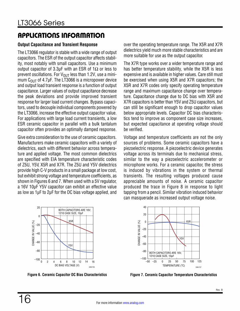
Figure 6. Ceramic Capacitor DC Bias Characteristics Figure 7. Ceramic Capacitor Temperature Characteristics
DC BIAS VOLTAGE (V)
CHAN
GE IN
VAL
UE (%
)
3066 F06
20
0
–20
–40
–60
–80
–1000 4 8 102 6 12 14
X5R
Y5V
16
BOTH CAPACITORS ARE 16V,1210 CASE SIZE, 10µF
TEMPERATURE (°C)–50
40
20
0
–20
–40
–60
–80
–10025 75
3066 F07
–25 0 50 100 125
Y5V
CHAN
GE IN
VAL
UE (%
) X5R
BOTH CAPACITORS ARE 16V,1210 CASE SIZE, 10µF
Output Capacitance and Transient Response
The LT3066 regulator is stable with a wide range of output capacitors. The ESR of the output capacitor affects stabil-ity, most notably with small capacitors. Use a minimum output capacitor of 3.3μF with an ESR of 1Ω or less to prevent oscillations. For VOUT less than 1.2V, use a mini-mum COUT of 4.7µF. The LT3066 is a micropower device and output load transient response is a function of output capacitance. Larger values of output capacitance decrease the peak deviations and provide improved transient response for larger load current changes. Bypass capaci-tors, used to decouple individual components powered by the LT3066, increase the effective output capacitor value. For applications with large load current transients, a low ESR ceramic capacitor in parallel with a bulk tantalum capacitor often provides an optimally damped response.
Give extra consideration to the use of ceramic capacitors. Manufacturers make ceramic capacitors with a variety of dielectrics, each with different behavior across tempera-ture and applied voltage. The most common dielectrics are specified with EIA temperature characteristic codes of Z5U, Y5V, X5R and X7R. The Z5U and Y5V dielectrics provide high C-V products in a small package at low cost, but exhibit strong voltage and temperature coefficients, as shown in Figures 6 and 7. When used with a 5V regulator, a 16V 10μF Y5V capacitor can exhibit an effective value as low as 1μF to 2μF for the DC bias voltage applied, and
over the operating temperature range. The X5R and X7R dielectrics yield much more stable characteristics and are more suitable for use as the output capacitor.
The X7R type works over a wider temperature range and has better temperature stability, while the X5R is less expensive and is available in higher values. Care still must be exercised when using X5R and X7R capacitors; the X5R and X7R codes only specify operating temperature range and maximum capacitance change over tempera-ture. Capacitance change due to DC bias with X5R and X7R capacitors is better than Y5V and Z5U capacitors, but can still be significant enough to drop capacitor values below appropriate levels. Capacitor DC bias characteris-tics tend to improve as component case size increases, but expected capacitance at operating voltage should be verified.
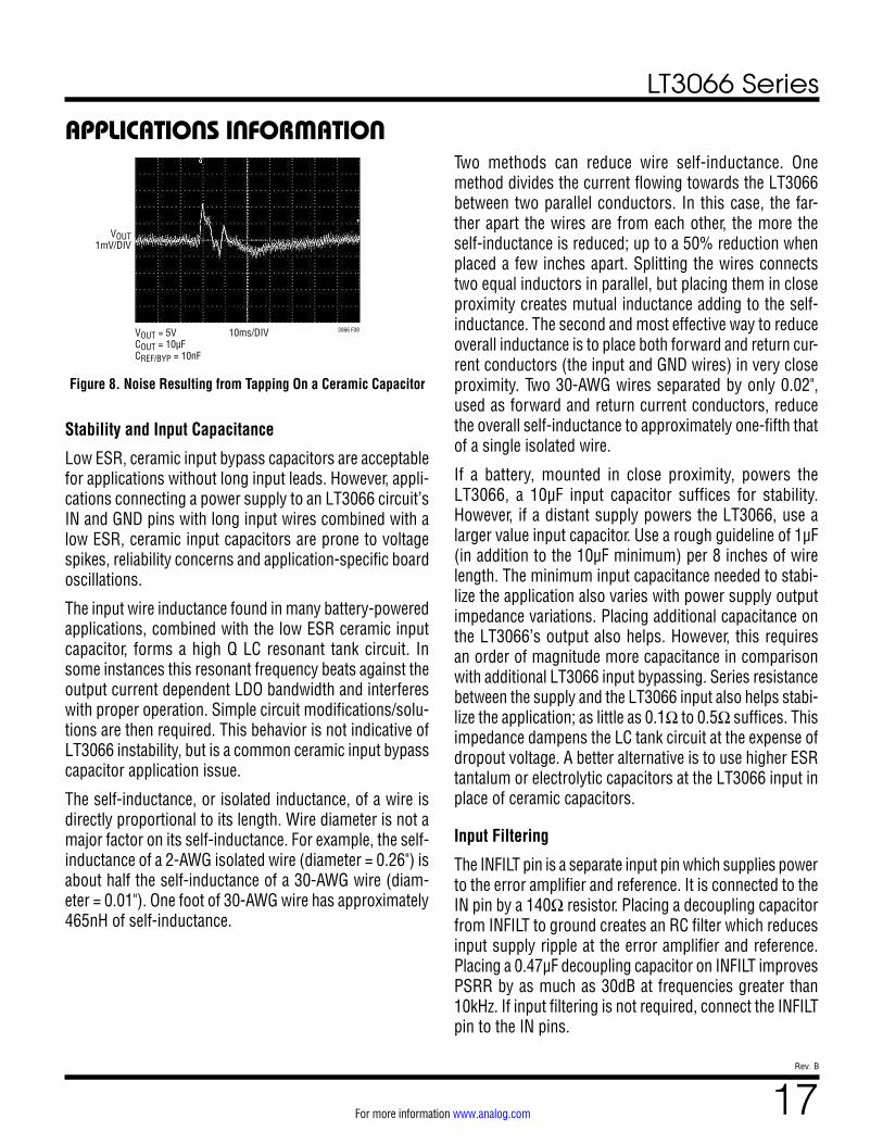
Voltage and temperature coefficients are not the only sources of problems. Some ceramic capacitors have a piezoelectric response. A piezoelectric device generates voltage across its terminals due to mechanical stress, similar to the way a piezoelectric accelerometer or microphone works. For a ceramic capacitor, the stress is induced by vibrations in the system or thermal transients. The resulting voltages produced cause appreciable amounts of noise. A ceramic capacitor produced the trace in Figure 8 in response to light tapping from a pencil. Similar vibration induced behavior can masquerade as increased output voltage noise.
LT3066 Series
17Rev. B
For more information www.analog.com
APPLICATIONS INFORMATION
Figure 8. Noise Resulting from Tapping On a Ceramic Capacitor
VOUT1mV/DIV
10ms/DIV 3066 F08VOUT = 5VCOUT = 10µFCREF/BYP = 10nF
Stability and Input Capacitance
Low ESR, ceramic input bypass capacitors are acceptable for applications without long input leads. However, appli-cations connecting a power supply to an LT3066 circuit’s IN and GND pins with long input wires combined with a low ESR, ceramic input capacitors are prone to voltage spikes, reliability concerns and application-specific board oscillations.
The input wire inductance found in many battery-powered applications, combined with the low ESR ceramic input capacitor, forms a high Q LC resonant tank circuit. In some instances this resonant frequency beats against the output current dependent LDO bandwidth and interferes with proper operation. Simple circuit modifications/solu-tions are then required. This behavior is not indicative of LT3066 instability, but is a common ceramic input bypass capacitor application issue.
The self-inductance, or isolated inductance, of a wire is directly proportional to its length. Wire diameter is not a major factor on its self-inductance. For example, the self-inductance of a 2-AWG isolated wire (diameter = 0.26") is about half the self-inductance of a 30-AWG wire (diam-eter = 0.01"). One foot of 30-AWG wire has approximately 465nH of self-inductance.
Two methods can reduce wire self-inductance. One method divides the current flowing towards the LT3066 between two parallel conductors. In this case, the far-ther apart the wires are from each other, the more the self-inductance is reduced; up to a 50% reduction when placed a few inches apart. Splitting the wires connects two equal inductors in parallel, but placing them in close proximity creates mutual inductance adding to the self-inductance. The second and most effective way to reduce overall inductance is to place both forward and return cur-rent conductors (the input and GND wires) in very close proximity. Two 30-AWG wires separated by only 0.02", used as forward and return current conductors, reduce the overall self-inductance to approximately one-fifth that of a single isolated wire.
If a battery, mounted in close proximity, powers the LT3066, a 10µF input capacitor suffices for stability. However, if a distant supply powers the LT3066, use a larger value input capacitor. Use a rough guideline of 1µF (in addition to the 10µF minimum) per 8 inches of wire length. The minimum input capacitance needed to stabi-lize the application also varies with power supply output impedance variations. Placing additional capacitance on the LT3066’s output also helps. However, this requires an order of magnitude more capacitance in comparison with additional LT3066 input bypassing. Series resistance between the supply and the LT3066 input also helps stabi-lize the application; as little as 0.1Ω to 0.5Ω suffices. This impedance dampens the LC tank circuit at the expense of dropout voltage. A better alternative is to use higher ESR tantalum or electrolytic capacitors at the LT3066 input in place of ceramic capacitors.
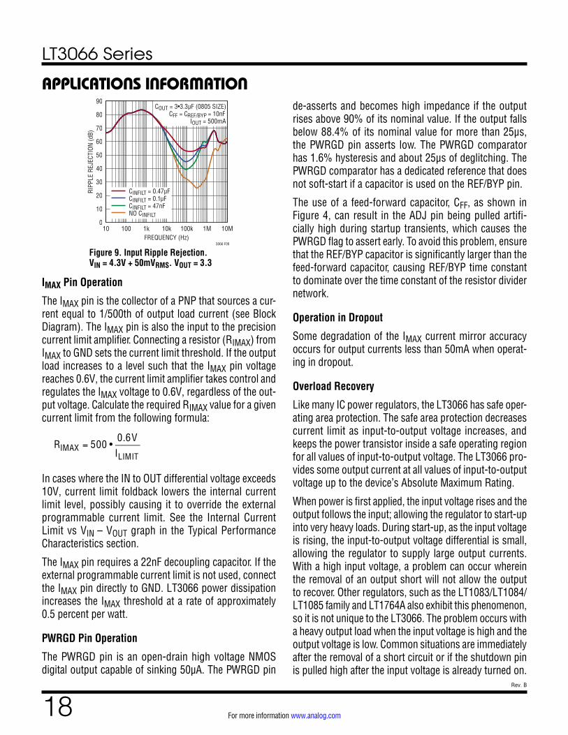
Input Filtering
The INFILT pin is a separate input pin which supplies power to the error amplifier and reference. It is connected to the IN pin by a 140Ω resistor. Placing a decoupling capacitor from INFILT to ground creates an RC filter which reduces input supply ripple at the error amplifier and reference. Placing a 0.47µF decoupling capacitor on INFILT improves PSRR by as much as 30dB at frequencies greater than 10kHz. If input filtering is not required, connect the INFILT pin to the IN pins.
LT3066 Series
18Rev. B
For more information www.analog.com
APPLICATIONS INFORMATION
Figure 9. Input Ripple Rejection. VIN = 4.3V + 50mVRMS. VOUT = 3.3
COUT = 3•3.3µF (0805 SIZE)CFF = CREF/BYP = 10nF
IOUT = 500mA
CINFILT = 0.47µFCINFILT = 0.1µFCINFILT = 47nFNO CINFILT
FREQUENCY (Hz)10 100 1k 10k 100k 1M 10M
0
10
20
30
40
50
60
70
80
90
RIPP
LE R
EJEC
TION
(dB)
VIN = 4.3V + 50mVRMS, VOUT = 3.3V
3066 F09
IMAX Pin Operation
The IMAX pin is the collector of a PNP that sources a cur-rent equal to 1/500th of output load current (see Block Diagram). The IMAX pin is also the input to the precision current limit amplifier. Connecting a resistor (RIMAX) from IMAX to GND sets the current limit threshold. If the output load increases to a level such that the IMAX pin voltage reaches 0.6V, the current limit amplifier takes control and regulates the IMAX voltage to 0.6V, regardless of the out-put voltage. Calculate the required RIMAX value for a given current limit from the following formula:
RIMAX = 500 •0.6VILIMIT
In cases where the IN to OUT differential voltage exceeds 10V, current limit foldback lowers the internal current limit level, possibly causing it to override the external programmable current limit. See the Internal Current Limit vs VIN – VOUT graph in the Typical Performance Characteristics section.
The IMAX pin requires a 22nF decoupling capacitor. If the external programmable current limit is not used, connect the IMAX pin directly to GND. LT3066 power dissipation increases the IMAX threshold at a rate of approximately 0.5 percent per watt.
PWRGD Pin Operation
The PWRGD pin is an open-drain high voltage NMOS digital output capable of sinking 50µA. The PWRGD pin
de-asserts and becomes high impedance if the output rises above 90% of its nominal value. If the output falls below 88.4% of its nominal value for more than 25μs, the PWRGD pin asserts low. The PWRGD comparator has 1.6% hysteresis and about 25μs of deglitching. The PWRGD comparator has a dedicated reference that does not soft-start if a capacitor is used on the REF/BYP pin.
The use of a feed-forward capacitor, CFF, as shown in Figure 4, can result in the ADJ pin being pulled artifi-cially high during startup transients, which causes the PWRGD flag to assert early. To avoid this problem, ensure that the REF/BYP capacitor is significantly larger than the feed-forward capacitor, causing REF/BYP time constant to dominate over the time constant of the resistor divider network.
Operation in Dropout
Some degradation of the IMAX current mirror accuracy occurs for output currents less than 50mA when operat-ing in dropout.
Overload Recovery
Like many IC power regulators, the LT3066 has safe oper-ating area protection. The safe area protection decreases current limit as input-to-output voltage increases, and keeps the power transistor inside a safe operating region for all values of input-to-output voltage. The LT3066 pro-vides some output current at all values of input-to-output voltage up to the device’s Absolute Maximum Rating.
When power is first applied, the input voltage rises and the output follows the input; allowing the regulator to start-up into very heavy loads. During start-up, as the input voltage is rising, the input-to-output voltage differential is small, allowing the regulator to supply large output currents. With a high input voltage, a problem can occur wherein the removal of an output short will not allow the output to recover. Other regulators, such as the LT1083/LT1084/LT1085 family and LT1764A also exhibit this phenomenon, so it is not unique to the LT3066. The problem occurs with a heavy output load when the input voltage is high and the output voltage is low. Common situations are immediately after the removal of a short circuit or if the shutdown pin is pulled high after the input voltage is already turned on.
LT3066 Series
19Rev. B
For more information www.analog.com
APPLICATIONS INFORMATION
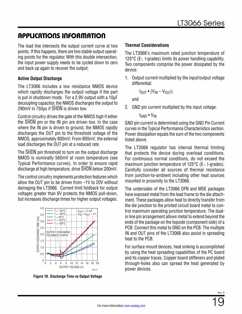
Figure 10. Discharge Time vs Output Voltage
COUT = 4.7µFVIN = VOUT + 1V
OUTPUT DISCHARGE FOLDBACK STARTS
T = –55°CT = –40°CT = 25°CT = 125°CT = 150°C
OUTPUT VOLTAGE (V)0 2 4 6 8 10 12 14 16 18 20
0
0.5
1.0
1.5
2.0
2.5
3.0
3.5
4.0
OUTP
UT D
ISCH
ARGE
TIM
E (m
s)
3066 F10
The load line intersects the output current curve at two points. If this happens, there are two stable output operat-ing points for the regulator. With this double intersection, the input power supply needs to be cycled down to zero and back up again to recover the output.
Active Output Discharge
The LT3066 includes a low resistance NMOS device which rapidly discharges the output voltage if the part is put in shutdown mode. For a 2.9V output with a 10μF decoupling capacitor, the NMOS discharges the output to 290mV in 750µs if SHDN is driven low.
Control circuitry drives the gate of the NMOS high if either the SHDN pin or the IN pin are driven low. In the case where the IN pin is driven to ground, the NMOS rapidly discharges the OUT pin to the threshold voltage of the NMOS, approximately 800mV. From 800mV, the external load discharges the OUT pin at a reduced rate.
The SHDN pin threshold to turn on the output discharge NMOS is nominally 560mV at room temperature (see Typical Performance curves). In order to ensure rapid discharge at high temperature, drive SHDN below 200mV.
The control circuitry implements protection features which allow the OUT pin to be driven from –1V to 20V without damaging the LT3066. Current limit foldback for output voltages greater than 6V protects the NMOS pull-down, but increases discharge times for higher output voltages.
Thermal Considerations
The LT3066’s maximum rated junction temperature of 125°C (E-, I-grades) limits its power handling capability. Two components comprise the power dissipated by the device:
1. Output current multiplied by the input/output voltage differential:
IOUT • (VIN – VOUT),
and
2. GND pin current multiplied by the input voltage:
IGND • VIN
GND pin current is determined using the GND Pin Current curves in the Typical Performance Characteristics section.Power dissipation equals the sum of the two components listed above.
The LT3066 regulator has internal thermal limiting that protects the device during overload conditions. For continuous normal conditions, do not exceed the maximum junction temperature of 125°C (E-, I-grades). Carefully consider all sources of thermal resistance from junction-to-ambient including other heat sources mounted in proximity to the LT3066.
The undersides of the LT3066 DFN and MSE packages have exposed metal from the lead frame to the die attach-ment. These packages allow heat to directly transfer from the die junction to the printed circuit board metal to con-trol maximum operating junction temperature. The dual-in line pin arrangement allows metal to extend beyond the ends of the package on the topside (component side) of a PCB. Connect this metal to GND on the PCB. The multiple IN and OUT pins of the LT3066 also assist in spreading heat to the PCB.
For surface mount devices, heat sinking is accomplished by using the heat spreading capabilities of the PC board and its copper traces. Copper board stiffeners and plated through-holes also can spread the heat generated by power devices.
LT3066 Series
20Rev. B
For more information www.analog.com
APPLICATIONS INFORMATION
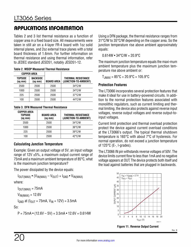
Figure 11. Reverse Output Current
VIN = VSHDN = 2.1VVADJ = VOUT
VOUT (V)0 2 4 6 8 10 12 14 16 18 20
0
5
10
15
20
25
30
35
40
45
50
OUPU
T CU
RREN
T (µ
A)
Reverse Current
3066 F11
Tables 2 and 3 list thermal resistance as a function of copper area in a fixed board size. All measurements were taken in still air on a 4-layer FR-4 board with 1oz solid internal planes, and 2oz external trace planes with a total board thickness of 1.6mm. For further information on thermal resistance and using thermal information, refer to JEDEC standard JESD51, notably JESD51-12.
Table 2. MSOP Measured Thermal ResistanceCOPPER AREA
BOARD AREATHERMAL RESISTANCE
(JUNCTION-TO-AMBIENT)TOPSIDE (sq mm)
BACKSIDE (sq mm)
2500 2500 2500 34°C/W
1000 2500 2500 34°C/W
225 2500 2500 37°C/W
100 2500 2500 44°C/W
Table 3. DFN Measured Thermal ResistanceCOPPER AREA
TOPSIDE (sq mm)
BOARD AREA (sq mm)
THERMAL RESISTANCE (JUNCTION-TO-AMBIENT)
2500 2500 34°C/W
1000 2500 36°C/W
225 2500 39°C/W
100 2500 42°C/W
Calculating Junction Temperature
Example: Given an output voltage of 5V, an input voltage range of 12V ±5%, a maximum output current range of 75mA and a maximum ambient temperature of 85°C, what is the maximum junction temperature?
The power dissipated by the device equals:
IOUT(MAX) • (VIN(MAX) – VOUT) + IGND • VIN(MAX)
where:
IOUT(MAX) = 75mA
VIN(MAX) = 12.6V
IGND at (IOUT = 75mA, VIN = 12V) = 3.5mA
So:
P = 75mA • (12.6V – 5V) + 3.5mA • 12.6V = 0.614W
Using a DFN package, the thermal resistance ranges from 31°C/W to 35°C/W depending on the copper area. So the junction temperature rise above ambient approximately equals:
0.614W • 34°C/W = 20.9°C
The maximum junction temperature equals the maxi-mum ambient temperature plus the maximum junction tem-perature rise above ambient or:
TJMAX = 85°C + 20.9°C = 105.9°C
Protection Features
The LT3066 incorporates several protection features that make it ideal for use in battery-powered circuits. In addi-tion to the normal protection features associated with monolithic regulators, such as current limiting and ther-mal limiting, the device also protects against reverse input voltages, reverse output voltages and reverse output-to-input voltages.
Current limit protection and thermal overload protection protect the device against current overload conditions at the LT3066’s output. The typical thermal shutdown temperature is 165°C with about 7°C of hysteresis. For normal operation, do not exceed a junction temperature of 125°C (E-, I-grades).
The LT3066 IN pin withstands reverse voltages of 50V. The device limits current flow to less than 1mA and no negative voltage appears at OUT. The device protects both itself and the load against batteries that are plugged in backwards.
LT3066 Series
21Rev. B
For more information www.analog.com
Programming Undervoltage Lockout
Power Supply Sequencing Using PWRGD
LT3066R1
IN
SHDN
R2
VIN > VUVLOIN
3066 TA02
VUVLO =
R1+R2R2
• 1.1V
LT3066IN
SHDN
IN
LT3066IN
SHDNPWRGD
3066 TA03
500k
TYPICAL APPLICATIONS
Current Monitor
RIMAX
TO ADC
LT3066
IMAX
3066 TA04
RIMAX =600mV
IOUT(MAX)
• 500
VIMAX =IOUT500
•RIMAX
LT3066 Series
22Rev. B
For more information www.analog.com
LED Driver/Current Source
LT3066
2k22nF
OUTIN
PWRGD
SHDN
IMAX
100k I = 100mA
6Ω
LED
10nF
3066 TA05
GND
REF/BYP
ADJ
5VIN
OPEN-LEDINDICATOR
SHDN
ILIM = 150mA
10µF
TYPICAL APPLICATIONS
Paralleling Regulators for Higher Output Current
LT3066
49.9Ω
IN
PWRGD
SHDN
OUT
ADJ
GND
REF/BYP
500k10µF 10µF
2.5V1A
6.04k1%
10nF
3066 TA06
19.1k1%
6.04k1%
21k1%
VIN > 3V
PWRGD
SHDN
IMAX
LT3066
49.9Ω
IN
PWRGD
SHDN
OUT
ADJ
GND
REF/BYP
10nF
0.1µF
IMAX
–
+ 10k
LT1637
1k
33nF
1k
6.8k
10µF 10µF
LT3066 Series
23Rev. B
For more information www.analog.com
PACKAGE DESCRIPTION
4.00 ±0.10(2 SIDES)
3.00 ±0.10(2 SIDES)
NOTE:1. DRAWING PROPOSED TO BE A VARIATION OF VERSION (WGED) IN JEDEC PACKAGE OUTLINE M0-2292. DRAWING NOT TO SCALE3. ALL DIMENSIONS ARE IN MILLIMETERS4. DIMENSIONS OF EXPOSED PAD ON BOTTOM OF PACKAGE DO NOT INCLUDE MOLD FLASH. MOLD FLASH, IF PRESENT, SHALL NOT EXCEED 0.15mm ON ANY SIDE5. EXPOSED PAD SHALL BE SOLDER PLATED6. SHADED AREA IS ONLY A REFERENCE FOR PIN 1 LOCATION ON THE TOP AND BOTTOM OF PACKAGE
0.40 ±0.10
BOTTOM VIEW—EXPOSED PAD
1.70 ±0.10
0.75 ±0.05
R = 0.115TYP
R = 0.05TYP
2.50 REF
16
127
PIN 1 NOTCHR = 0.20 OR0.35 × 45°CHAMFER
PIN 1TOP MARK
(NOTE 6)
0.200 REF
0.00 – 0.05
(UE12/DE12) DFN 0806 REV D
2.50 REF
RECOMMENDED SOLDER PAD PITCH AND DIMENSIONSAPPLY SOLDER MASK TO AREAS THAT ARE NOT SOLDERED
2.20 ±0.05
0.70 ±0.05
3.60 ±0.05
PACKAGE OUTLINE
3.30 ±0.10
0.25 ±0.050.50 BSC
1.70 ±0.05
3.30 ±0.05
0.50 BSC0.25 ±0.05
DE/UE Package12-Lead Plastic DFN (4mm × 3mm)
(Reference LTC DWG # 05-08-1695 Rev D)
LT3066 Series
24Rev. B
For more information www.analog.com
PACKAGE DESCRIPTION
MSOP (MSE12) 0213 REV G
0.53 ±0.152(.021 ±.006)
SEATINGPLANE
0.18(.007)
1.10(.043)MAX
0.22 – 0.38(.009 – .015)
TYP
0.86(.034)REF
0.650(.0256)
BSC
12
12 11 10 9 8 7
7
DETAIL “B”
1 6
NOTE:1. DIMENSIONS IN MILLIMETER/(INCH)2. DRAWING NOT TO SCALE3. DIMENSION DOES NOT INCLUDE MOLD FLASH, PROTRUSIONS OR GATE BURRS. MOLD FLASH, PROTRUSIONS OR GATE BURRS SHALL NOT EXCEED 0.152mm (.006") PER SIDE4. DIMENSION DOES NOT INCLUDE INTERLEAD FLASH OR PROTRUSIONS. INTERLEAD FLASH OR PROTRUSIONS SHALL NOT EXCEED 0.152mm (.006") PER SIDE5. LEAD COPLANARITY (BOTTOM OF LEADS AFTER FORMING) SHALL BE 0.102mm (.004") MAX6. EXPOSED PAD DIMENSION DOES INCLUDE MOLD FLASH. MOLD FLASH ON E-PAD SHALL NOT EXCEED 0.254mm (.010") PER SIDE.
0.254(.010) 0° – 6° TYP
DETAIL “A”
DETAIL “A”
GAUGE PLANE
RECOMMENDED SOLDER PAD LAYOUT
BOTTOM VIEW OFEXPOSED PAD OPTION
2.845 ±0.102(.112 ±.004)2.845 ±0.102
(.112 ±.004)
4.039 ±0.102(.159 ±.004)
(NOTE 3)
1.651 ±0.102(.065 ±.004)
1.651 ±0.102(.065 ±.004)
0.1016 ±0.0508(.004 ±.002)
1 2 3 4 5 6
3.00 ±0.102(.118 ±.004)
(NOTE 4)
0.406 ±0.076(.016 ±.003)
REF
4.90 ±0.152(.193 ±.006)
DETAIL “B”CORNER TAIL IS PART OF
THE LEADFRAME FEATURE.FOR REFERENCE ONLY
NO MEASUREMENT PURPOSE
0.12 REF
0.35REF
5.10(.201)MIN
3.20 – 3.45(.126 – .136)
0.889 ±0.127(.035 ±.005)
0.42 ±0.038(.0165 ±.0015)
TYP
0.65(.0256)
BSC
MSE Package12-Lead Plastic MSOP, Exposed Die Pad
(Reference LTC DWG # 05-08-1666 Rev G)
LT3066 Series
25Rev. B
For more information www.analog.com
REVISION HISTORYREV DATE DESCRIPTION PAGE NUMBER
A 05/16 Add –3.3V, –5V fixed voltage options. 1–26
B 10/18 Change typical minimum input voltage from 1.8V to 1.6VUpdate Minimum Input Voltage graph in Typical Performance SectionAdd 10µF output capacitor to figure TA05Update Related Parts section with new 1.6V minimum VIN (LT3050/LT3055/LT3060/LT3065)
1, 3, 148
2226
Information furnished by Analog Devices is believed to be accurate and reliable. However, no responsibility is assumed by Analog Devices for its use, nor for any infringements of patents or other rights of third parties that may result from its use. Specifications subject to change without notice. No license is granted by implication or otherwise under any patent or patent rights of Analog Devices.
LT3066 Series
26Rev. B
For more information www.analog.com
RELATED PARTS
TYPICAL APPLICATIONAdjustable High Efficiency Regulator
LT3066
GND
IN
SHDN
PWRGD
REF/BYP
OUT
ADJ
IMAX
10µF
0.6V TO 10VOUT200mA
61.9k1%
1.2k22nF
100k
255k
10k
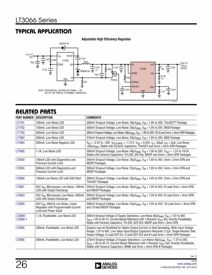
NOTE: DIFFERENTIAL VOLTAGE ON LT3066 ≈ 1.4V SET BY THE TP0610L P-CHANNEL THRESHOLD.
TP0610L
47µF×2MBRM140
4.7µF
10nF
10nF
3066 TA07
1M
LT3493
CMDSH-4E
GND
10µH
VIN
SHDN
BOOST
SW
FB
0.1µF100k
0.1µF
1µF10µF
4.5V TO25V
PART NUMBER DESCRIPTION COMMENTS
LT1761 100mA, Low Noise LDO 300mV Dropout Voltage, Low Noise: 20μVRMS, VIN = 1.8V to 20V, ThinSOT™ Package
LT1762 150mA, Low Noise LDO 300mV Dropout Voltage, Low Noise: 20μVRMS, VIN = 1.8V to 20V, MS8 Package
LT1763 500mA, Low Noise LDO 300mV Dropout Voltage, Low Noise: 20μVRMS, VIN = 1.8V to 20V, SO-8 and 3mm × 4mm DFN Packages
LT1962 300mA, Low Noise LDO 270mV Dropout Voltage, Low Noise: 20μVRMS, VIN = 1.8V to 20V, MS8 Package
LT1964 200mA, Low Noise Negative LDO VIN = –2.2V to –20V, VOUT(MIN) = –1.21V, VDO = 0.34V, IQ = 30μA, ISD = 3μA, Low Noise <30μVRMS, Stable with Ceramic Capacitors, ThinSOT and 3mm × 3mm DFN Packages
LT1965 1.1A, Low Noise LDO 290mV Dropout Voltage, Low Noise: 40μVRMS, VIN = 1.8V to 20V, VOUT = 1.2V to 19.5V, Stable with Ceramic Capacitors, TO-220, DD-Pak, MSOP and 3mm × 3mm DFN Packages
LT3050 100mA LDO with Diagnostics and Precision Current Limit
340mV Dropout Voltage, Low Noise: 30μVRMS, VIN = 1.6V to 45V, 3mm × 2mm DFN and MSOP Packages
LT3055 500mA LDO with Diagnostics and Precision Current Limit
350mV Dropout Voltage, Low Noise: 25μVRMS, VIN = 1.6V to 45V, 4mm × 3mm DFN and MSOP Packages
LT3060 100mA Low Noise LDO with Soft-Start 300mV Dropout Voltage, Low Noise: 30μVRMS, VIN = 1.6V to 45V, 2mm × 2mm DFN and ThinSOT Packages
LT3061 45V VIN, Micropower, Low Noise, 100mA LDO with Output Discharge
250mV Dropout Voltage, Low Noise: 30μVRMS, VIN = 1.6V to 45V, 8-Lead 2mm × 3mm DFN and MSOP Packages
LT3063 45V VIN, Micropower, Low Noise, 200mA LDO with Output Discharge
300mV Dropout Voltage, Low Noise: 30μVRMS, VIN = 1.6V to 45V, 8-Lead 2mm × 3mm DFN and MSOP Packages
LT3065 45V VIN, 500mA Low Noise, Linear Regulator with Programmable Current Limit and Power Good
300mV Dropout Voltage, Low Noise: 25μVRMS, VIN = 1.6V to 45V, 10-Lead 3mm × 3mm DFN and 12-lead MSOP Packages
LT3080/ LT3080-1
1.1A, Parallelable, Low Noise LDO 300mV Dropout Voltage (2-Supply Operation), Low Noise 40µVRMS, VIN = 1.2V to 36V, VOUT = 0V to 35.7V, Current-Based Reference with 1-Resistor VOUT Set, Directly Parallelable, Stable with Ceramic Capacitors, TO-220, SOT-223, MSOP and 3mm × 3mm DFN
LT3082 200mA, Parallelable, Low Noise LDO Outputs may be Paralleled for Higher Output Current or Heat Spreading, Wide Input Voltage Range: 1.2V to 40V, Low Value Input/Output Capacitors Required: 2.2µF, Single Resistor Sets Output Voltage, 8-Lead SOT-23, 3-Lead SOT-223 and 8-Lead 3mm × 3mm DFN Packages
LT3085 500mA, Parallelable, Low Noise LDO 275mV Dropout Voltage (2-Supply Operation), Low Noise 40µVRMS, VIN = 1.2V to 36V, VOUT = 0V to 35.7V, Current-Based Reference with 1-Resistor VOUT Set, Directly Parallelable, Stable with Ceramic Capacitors, MS8E and 2mm × 3mm DFN-6 Packages
ANALOG DEVICES, INC. 2015-2018
10/18www.analog.com


![Acta Medica Okayamaeprints.lib.okayama-u.ac.jp/files/public/3/30665/...2 Acta Medica Okayama, Vol. 36 [1982], Iss. 6, Art. 7](https://img.pdfslide.net/doc/110x75/5c69826109d3f242168d1f80/acta-medica-acta-medica-okayama-vol-36-1982-iss-6-art-7-.jpg)