Embed Size (px)
Citation preview

LT3652HV
13652hvfb
For more information www.linear.com/LT3652HV
TYPICAL APPLICATION
DESCRIPTION
Power Tracking 2A Battery Charger
The LT®3652HV is a complete monolithic step-down bat-tery charger that operates over a 4.95V to 34V input range. The LT3652HV provides a constant-current/constant-voltage charge characteristic, with maximum charge current externally programmable up to 2A. The charger employs a 3.3V float voltage feedback reference, so any desired battery float voltage up to 18V can be programmed with a resistor divider.
The LT3652HV employs an input voltage regulation loop, which reduces charge current if the input voltage falls below a programmed level, set with a resistor divider. When the LT3652HV is powered by a solar panel, the input regulation loop is used to maintain the panel at peak output power.
The LT3652HV can be configured to terminate charging when charge current falls below 1/10 of the programmed maximum (C/10). Once charging is terminated, the LT3652HV enters a low-current (85µA) standby mode. An auto-recharge feature starts a new charging cycle if the battery voltage falls 2.5% below the programmed float voltage. The LT3652HV also contains a programmable safety timer, used to terminate charging after a desired time is reached. This allows top-off charging at currents less than C/10.
FEATURES
APPLICATIONS
n Input Supply Voltage Regulation Loop for Peak Power Tracking in (MPPT) Solar Applications
n Wide Input Voltage Range: 4.95V to 34V (40V Abs Max)n Programmable Charge Rate Up to 2An User Selectable Termination: C/10 or On-Board
Termination Timern Resistor Programmable Float Voltage Up to 18V
Accommodates 4-Cell Li-Ion/Polymer, 5-Cell LiFePO4, Lead-Acid Chemistries
n Parallelable for Higher Output Currentn 1MHz Fixed Frequencyn 0.5% Float Voltage Reference Accuracyn 5% Charge Current Accuracyn 2.5% C/10 Detection Accuracyn Binary-Coded Open-Collector Status Pinsn Thermally Enhanced 3mm × 3mm DFN and MSE
Packages
n Solar Powered Applicationsn Remote Monitoring Stations n Portable Handheld Instruments n 12V to 24V Automotive Systemsn Battery Charging from Current Limited Adapter L, LT, LTC, LTM, Linear Technology and the Linear logo are registered trademarks and
PowerPath is a trademark of Linear Technology Corporation. All other trademarks are the property of their respective owners.
VIN_REG Loop Servos Maximum Charge Current to Prevent AC Adapter Output from Drooping Lower Than 24V 5-Cell LiFePO4 Charger (18V at 1.5A) with C/10 Termination
Powered by Inexpensive 24VDC/1A Unregulated Wall Adapter.
SWVIN
AC ADAPTERINPUT
24VDC AT 1AVIN_REG
VFB
BOOST
SENSE
BAT
NTC
TIMER
1µF 10V 1N4148
127k
3652 TA01a
R110KB = 3380
10µF
20µH
10µF
5-CELL LiFePO4 PACK(18V FLOAT)
SYSTEMLOAD
+
LT3652HV
44.2k
750k
MBRS340D3
MBRS340
51.1k
SHDN
CHRG
FAULT
150k
665k
0.068
ADAPTER OUTPUT CURRENT (A)0 0.2
ADAP
TER
OUTP
UT V
OLTA
GE (V
)
12
15
18
33
30
27
24
21
0.6 1 1.2
3652 TA01b
36
0.4 0.8 1.61.4 21.8
1A/24VDC Unregulated Adapter I vs V Characteristic

LT3652HV
23652hvfb
For more information www.linear.com/LT3652HV
PIN CONFIGURATION
ABSOLUTE MAXIMUM RATINGS
Voltages: VIN ........................................................................40V VIN_REG, SHDN, CHRG, FAULT ............ VIN + 0.5V, 40V SW ........................................................................40V SW-VIN.................................................................4.5V BOOST ...................................................SW+10V, 50V BAT, SENSE ...........................................................20V
(Note 1)
ORDER INFORMATIONLEAD FREE FINISH TAPE AND REEL PART MARKING* PACKAGE DESCRIPTION TEMPERATURE RANGE
LT3652HVEDD#PBF LT3652HVEDD#TRPBF LFRG 12-Lead Plastic DFN 3mm × 3mm –40°C to 125°C
LT3652HVIDD#PBF LT3652HVIDD#TRPBF LFRG 12-Lead Plastic DFN 3mm × 3mm –40°C to 125°C
LT3652HVEMSE#PBF LT3652HVEMSE#TRPBF 3652HV 12-Lead Plastic MSOP –40°C to 125°C
LT3652HVIMSE#PBF LT3652HVIMSE#TRPBF 3652HV 12-Lead Plastic MSOP –40°C to 125°C
Consult LTC Marketing for parts specified with wider operating temperature ranges. *The temperature grade is identified by a label on the shipping container.For more information on lead free part marking, go to: http://www.linear.com/leadfree/ For more information on tape and reel specifications, go to: http://www.linear.com/tapeandreel/. Some packages are available in 500 unit reels through designated sales channels with #TRMPBF suffix.
TOP VIEW
DD PACKAGE12-LEAD (3mm × 3mm) PLASTIC DFN
12
11
8
9
104
5
3
2
1 SW
BOOST
SENSE
BAT
NTC
VFB
VIN
VIN_REG
SHDN
CHRG
FAULT
TIMER 6 7
13GND
123456
VINVIN_REGSHDNCHRGFAULTTIMER
121110987
SWBOOSTSENSEBATNTCVFB
TOP VIEW
13GND
MSE PACKAGE12-LEAD PLASTIC MSOP
TJMAX = 125°C, θJA = 43°C/W, θJC = 3°C/W EXPOSED PAD (PIN 13) IS GND, MUST BE SOLDERED TO PCB
TJMAX = 125°C, θJA = 43°C/W, θJC = 3°C/W EXPOSED PAD (PIN 13) IS GND, MUST BE SOLDERED TO PCB
BAT-SENSE ......................................... –0.5V to +0.5V NTC, TIMER, ........................................................2.5V VFB ..........................................................................5VOperating Junction Temperature Range
(Note 2) ............................................. –40°C to 125°CStorage Temperature Range ................... –65°C to 150°C

LT3652HV
33652hvfb
For more information www.linear.com/LT3652HV
SYMBOL PARAMETER CONDITIONS MIN TYP MAX UNITS
VIN VIN Operating Range VIN Start Voltage
VBAT = 4.2 (Notes 3, 4) VBAT = 4.2 (Note 4)
l
l
4.95 7.5
34 V V
VIN(OVLO) OVLO Threshold OVLO Hysteresis
VIN Rising l 34 35 1
40 V V
VIN(UVLO) UVLO Threshold UVLO Hysteresis
VIN Rising 4.6 0.2
4.95 V V
VFB(FLT) Float Voltage Reference (Note 6)
l
3.282 3.26
3.3 3.318 3.34
V V
ΔVRECHARGE Recharge Reference Threshold Voltage Relative to VFB(FLT) (Note 6) 82.5 mV
VFB(PRE) Reference Precondition Threshold VFB Rising (Note 6) 2.3 V
VFB(PREHYST) Reference Precondition Threshold Hysteresis
Voltage Relative to VFB(PRE) (Note 6) 70 mV
VIN_REG(TH) Input Regulation Reference VFB = 3V; VSENSE – VBAT = 50mV l 2.65 2.7 2.75 V
IIN_REG Input Regulation Reference Bias Current VIN_REG = VIN_REG(TH) l 35 100 nA
IVIN Operating Input Supply Current CC/CV Mode, ISW = 0 Standby Mode Shutdown (SHDN = 0)
l 2.5 85 15
3.5 mA µA µA
IBOOST BOOST Supply Current Switch On, ISW = 0, 2.5 < V(BOOST – SW) < 8.5
20 mA
IBOOST/ISW BOOST Switch Drive ISW = 2A 30 mA/A
VSW(ON) Switch-On Voltage Drop VIN – VSW, ISW = 2A 350 mV
ISW(MAX) Switch Current Limit l 2.5 3 A
VSENSE(PRE) Precondition Sense Voltage VSENSE – VBAT; VFB = 2V 15 mV
VSENSE(DC) Maximum Sense Voltage VSENSE – VBAT; VFB = 3V (Note 7) l 95 100 105 mV
VSENSE(C/10) C/10 Trigger Sense Voltage VSENSE – VBAT, Falling l 7.5 10 12.5 mV
IBAT BAT Input Bias Current Charging Terminated 0.1 1 µA
ISENSE SENSE Input Bias Current Charging Terminated 0.1 1 µA
IVFB VFB Input Bias Current Charging Terminated 65 nA
IVFB VFB Input Bias Current CV Operation (Note 5) 110 nA
VNTC(H) NTC Range Limit (High) VNTC Rising l 1.25 1.36 1.45 V
VNTC(L) NTC Range Limit (Low) VNTC Falling l 0.27 0.29 0.315 V
VNTC(HYST) NTC Threshold Hysteresis % of threshold 20 %
RNTC(DIS) NTC Disable Impedance Impedance to ground l 250 500 kΩ
INTC NTC Bias Current VNTC = 0.8V l 47.5 50 52.5 µA
VSHDN Shutdown Threshold Rising l 1.15 1.2 1.25 V
VSHDN(HYST) Shutdown Hysteresis 120 mV
ISHDN SHDN Input Bias Current –10 nA
VCHRG, VFAULT Status Low Voltage 10mA Load l 0.4 V
ITIMER Charge/Discharge Current 25 µA
VTIMER(DIS) Timer Disable Threshold l 0.1 0.25 V
The l denotes the specifications which apply over the full operating junction temperature range, otherwise specifications are at TA = 25°C (Note 2). VIN = 20V, Boost – SW = 4V, SHDN = 2V, VFB = 3.3V, CTIMER = 0.68µF.ELECTRICAL CHARACTERISTICS

LT3652HV
43652hvfb
For more information www.linear.com/LT3652HV
SYMBOL PARAMETER CONDITIONS MIN TYP MAX UNITS
tTIMER Full Charge Cycle Timeout 3 hr
Precondition Timeout 22.5 min
Timer Accuracy l –10 10 %
fO Operating Frequency 1 MHz
DC Duty Cycle Range Continuous Operation l 15 90 %
The l denotes the specifications which apply over the full operating junction temperature range, otherwise specifications are at TA = 25°C (Note 2). VIN = 20V, Boost – SW = 4V, SHDN = 2V, VFB = 3.3V, CTIMER = 0.68µF.
Note 1: Stresses beyond those listed under Absolute Maximum Ratings may cause permanent damage to the device. Exposure to any Absolute Maximum Rating condition for extended periods may affect device reliability and lifetime.Note 2: The LT3652HV is tested under pulsed load conditions such that TJ ≅ TA. The LT3652HVE is guaranteed to meet performance specifications from 0°C to 85°C junction temperature. Specifications over the –40°C to 125°C operating junction temperature range are assured by design, characterization, and correlation with statistical process controls. The LT3652HVI specifications are guaranteed over the full –40°C to 125°C operating junction temperature range. Note that the maximum ambient temperature consistent with these specifications is determined by specific operating conditions in conjunction with board layout, the rated package thermal impedance and other environmental factors.
Note 3: VIN minimum voltages below the start threshold are only supported if (VBOOST-VSW) > 2V.Note 4: This parameter is valid for programmed output battery float voltages ≤ 4.2V. VIN operating range minimum is 0.75V above the programmed output battery float voltage (VBAT(FLT) + 0.75V). VIN Start Voltage is 3.3V above the programmed output battery float voltage (VBAT(FLT) + 3.3V).Note 5: Output battery float voltage (VBAT(FLT)) programming resistor divider equivalent resistance = 250k compensates for input bias current. Note 6: All VFB voltages measured through 250k series resistance.Note 7: VSENSE(DC) is reduced by thermal foldback as junction temperature approaches 125°C.
ELECTRICAL CHARACTERISTICS

LT3652HV
53652hvfb
For more information www.linear.com/LT3652HV
TYPICAL PERFORMANCE CHARACTERISTICS
Switch Forward Drop (VIN – VSW) vs Temperature
CC/CV Charging; SENSE Pin Bias Current vs VSENSE
C/10 Threshold (VSENSE–VBAT) vs Temperature
VFB Reference Voltage vs Temperature
VIN Standby Mode Current vs Temperature
Switch Drive (ISW/IBOOST) vs Switch Current
TJ = 25°C, unless otherwise noted.
TEMPERATURE (°C)–50
V FB
(FLT
)
3.296
3.298
3.300
3.302
0 50 75
3652 G01a
3.304
–25 25 100 125TEMPERATURE (°C)
–5065
I VIN
CUR
RENT
(µA)
70
75
80
100
90
0 50 75
3652 G02
95
85
–25 25 100
SWITCH CURRENT (A)0
I SW
/I BOO
ST
18
24
30
36
1.6
12
6
0
21
27
33
15
9
3
0.4 0.8 1.20.2 1.80.6 1.0 1.4 2.0
3652 G03
TEMPERATURE (°C)–50
320
V SW
(ON)
(mV)
340
360
380
480
420
0 50 75
3652 G04
440
460
400
–25 25 100 125
ISW = 2A
VSENSE (V)0
–350
I SEN
SE (µ
A)
–250
–150
–50
100
1 2 2.5
50
–300
–200
–100
0
0.5 1.5
3652 G05
VBAT = VBAT(PRE)
VBAT = VBAT(FLT)
TEMPERATURE (°C)–50
8
V SEN
SE(C
/10)
(mV)
9
10
11
12
0 50 75
3652 G06
–25 25 100 125
TEMPERATURE (°C)–50
V IN_
REG(
TH) (
V)
2.680
2.685
2.690
2.715
2.710
2.705
2.700
2.695
0 50 75
3652 G01
2.720
–25 25 100 125
VIN_REG Threshold vs Temperature: ICHG at 50%

LT3652HV
63652hvfb
For more information www.linear.com/LT3652HV
TYPICAL PERFORMANCE CHARACTERISTICS
Maximum Charge Current (VSENSE–VBAT) vs Temperature
Thermal Foldback – Maximum Charge Current (VSENSE–VBAT) vs Temperature
CC/CV Charging; BAT Pin Bias Current vs VBAT
TA = 25°C, unless otherwise noted.
TEMPERATURE (°C)–50
99.0
V SEN
SE(D
C) (m
V)
99.2
99.6
99.8
100.0
101.0
100.4
0 50 75
3652 G07
99.4
100.6
100.8
100.2
–25 25 100 125
VFB = 3V
TEMPERATURE (°C)
0
V SEN
SE(D
C) (m
V)40
80
20
60
100
120
45 65 85 105 12535 13525 55 75 95 115
3652 G08
VBAT (V)0
–0.4
I BAT
(mA)
0.0
0.4
0.8
2.2
1.6
1 2 2.5
2.0
1.2
–0.2
0.2
0.6
1.0
1.8
1.4
0.5 1.5 3
3652 G09
VBAT(FLT)
VIN_REG (V)2.65
V SEN
SE(D
C) (m
V)
0
20
80
60
40
2.67 2.69 2.7
3652 G10
100
2.66 2.68 2.722.71 2.73 2.74 2.75
VBAT(FLT) (V)0 2
0
I RFB
(µA)
8
6
10
12
18
3652 G11
4
2
64 8 10 12 1614
TIME (MINUTES)0
EFFICIENCY (%)
CHAR
GE C
URRE
NT (A
); PO
WER
LOS
S (W
)
0
0.5
2.0
2.5
1.5
1.0
40 80 100
3652 G12
3.0
35
45
75
65
55
95
85
20 60 140120 160 180 200
CHARGECURRENT
EFFICIENCY
POWERLOSS
VIN = 20V
Maximum Charge Current (VSENSE–VBAT) vs VIN_REG Voltage
VFLOAT Programming Resistor Current vs VFLOAT for 2-Resistor Network
Charge Current, Efficiency, and Power Loss vs Time (ICHG(MAX) = 2A; VFLOAT = 8.2V)
Charger Efficiency vs Battery Voltage (ICHG = 2A)
VBAT (V)
70
EFFI
CIEN
CY (%
)
76
80
82
84
86
88
74
72
78
90
5 7 9 11 134 14 153 6 8 10 12
3652 G13
VIN = 20V WITH INPUT BLOCKING DIODE
Battery Bias Current with Charger Disabled (IBAT + ISENSE + IBOOST + ISW)
VBAT (V)0
0
BATT
ERY
CURR
ENT
(µA)
2
6
8
10
12
18
3652 F14
4
62 1484 1610 18
12
14
16
VIN FLOATING
VIN = 20VVSHDN = 0V

LT3652HV
73652hvfb
For more information www.linear.com/LT3652HV
PIN FUNCTIONSVIN (Pin 1): Charger Input Supply. VIN operating range is 4.95V to 34V. VIN must be 3.3V greater than the pro-grammed output battery float voltage (VBAT(FLT)) for reli-able start-up. (VIN – VBAT(FLT)) ≥ 0.75V is the minimum operating voltage, provided (VBOOST – VSW) ≥ 2V. IVIN ~ 85µA after charge termination. This pin is typically con-nected to the cathode of a blocking diode.
VIN_REG (Pin 2): Input Voltage Regulation Reference. Maxi-mum charge current is reduced when this pin is below 2.7V. Connecting a resistor divider from VIN to this pin enables programming of minimum operational VIN voltage. This is typically used to program the peak power voltage for a solar panel. The LT3652HV servos the maximum charge current required to maintain the programmed operational VIN voltage, through maintaining the voltage on VIN_REG at or above 2.7V. If the voltage regulation feature is not used, connect the pin to VIN.
SHDN (Pin 3): Precision Threshold Shutdown Pin. The enable threshold is 1.2V (rising), with 120mV of input hysteresis. When in shutdown mode, all charging functions are disabled. The precision threshold allows use of the SHDN pin to incorporate UVLO functions. If the SHDN pin is pulled below 0.4V, the IC enters a low current shutdown mode where VIN current is reduced to 15µA. Typical SHDN pin input bias current is 10nA. If the shutdown function is not desired, connect the pin to VIN.
CHRG (Pin 4): Open-Collector Charger Status Output; typically pulled up through a resistor to a reference volt-age. This status pin can be pulled up to voltages as high as VIN when disabled, and can sink currents up to 10mA when enabled. During a battery charging cycle, if required charge current is greater than 1/10 of the programmed maximum current (C/10), CHRG is pulled low. A tem-perature fault also causes this pin to be pulled low. After C/10 charge termination or, if the internal timer is used for termination and charge current is less than C/10, the CHRG pin remains high-impedance.
FAULT (Pin 5): Open-Collector Charger Status Output; typically pulled up through a resistor to a reference volt-age. This status pin can be pulled up to voltages as high as VIN when disabled, and can sink currents up to 10mA when enabled. This pin indicates fault conditions during a
battery charging cycle. A temperature fault causes this pin to be pulled low. If the internal timer is used for termina-tion, a bad battery fault also causes this pin to be pulled low. If no fault conditions exist, the FAULT pin remains high-impedance.
TIMER (Pin 6): End-Of-Cycle Timer Programming Pin. If a timer-based charge termination is desired, connect a capacitor from this pin to ground. Full charge end-of-cycle time (in hours) is programmed with this capacitor following the equation:
tEOC = CTIMER • 4.4 • 106
A bad battery fault is generated if the battery does not achieve the precondition threshold voltage within one-eighth of tEOC, or:
tPRE = CTIMER • 5.5 • 105
A 0.68µF capacitor is typically used, which generates a timer EOC at three hours, and a precondition limit time of 22.5 minutes. If a timer-based termination is not desired, the timer function is disabled by connecting the TIMER pin to ground. With the timer function disabled, charging terminates when the charge current drops below a C/10 threshold, or ICHG(MAX)/10
VFB (Pin 7): Battery Float Voltage Feedback Reference. The charge function operates to achieve a final float voltage of 3.3V on this pin. Output battery float voltage (VBAT(FLT)) is programmed using a resistor divider. VBAT(FLT) can be programmed up to 18V.
The auto-restart feature initiates a new charging cycle when the voltage at the VFB pin falls 2.5% below the float voltage reference.
The VFB pin input bias current is 110nA. Using a resistor divider with an equivalent input resistance at the VFB pin of 250k compensates for input bias current error.
Required resistor values to program desired VBAT(FLT) follow the equations:
R1 = (VBAT(FLT) • 2.5 • 105)/3.3 (Ω)
R2 = (R1 • 2.5 • 105)/(R1 - (2.5 • 105)) (Ω)
R1 is connected from BAT to VFB, and R2 is connected from VFB to ground.

LT3652HV
83652hvfb
For more information www.linear.com/LT3652HV
NTC (Pin 8): Battery Temperature Monitor Pin. This pin is the input to the NTC (Negative Temperature Coefficient) thermistor temperature monitoring circuit. This function is enabled by connecting a 10kΩ, B = 3380 NTC thermistor from the NTC pin to ground. The pin sources 50µA, and monitors the voltage across the 10kΩ thermistor. When the voltage on this pin is above 1.36 (T < 0°C) or below 0.29V (T > 40°C), charging is disabled and the CHRG and FAULT pins are both pulled low. If internal timer termina-tion is being used, the timer is paused, suspending the charging cycle. Charging resumes when the voltage on NTC returns to within the 0.29V to 1.36V active region. There is approximately 5°C of temperature hysteresis associated with each of the temperature thresholds. The temperature monitoring function remains enabled while the thermistor resistance to ground is less than 250k, so if this function is not desired, leave the NTC pin unconnected.
BAT (Pin 9): Charger Output Monitor Pin. Connect a 10µF decoupling capacitance (CBAT) to ground. Depend-ing on application requirements, larger value decoupling capacitors may be required. The charge function operates to achieve the programmed output battery float voltage (VBAT(FLT)) at this pin. This pin is also the reference for the current sense voltage. Once a charge cycle is termi-nated, the input bias current of the BAT pin is reduced to < 0.1µA, to minimize battery discharge while the charger remains connected.
SENSE (Pin 10): Charge Current Sense Pin. Connect the inductor sense resistor (RSENSE) from the SENSE pin to the BAT pin. The voltage across this resistor sets the average
charge current. The maximum charge current (ICHG(MAX)) corresponds to 100mV across the sense resistor. This resistor can be set to program maximum charge cur-rent as high as 2A. The sense resistor value follows the relation:
RSENSE = 0.1/ICHG(MAX) (Ω)
Once a charge cycle is terminated, the input bias current of the SENSE pin is reduced to < 0.1µA, to minimize battery discharge while the charger remains connected.
BOOST (Pin 11): Bootstrapped Supply Rail for Switch Drive. This pin facilitates saturation of the switch transistor. Connect a 1µF or greater capacitor from the BOOST pin to the SW pin. Operating range of this pin is 0V to 8.5V, referenced to the SW pin. The voltage on the decoupling capacitor is refreshed through a rectifying diode, with the anode connected to either the battery output voltage or an external source, and the cathode connected to the BOOST pin.
SW (Pin 12): Switch Output Pin. This pin is the output of the charger switch, and corresponds to the emitter of the switch transistor. When enabled, the switch shorts the SW pin to the VIN supply. The drive circuitry for this switch is bootstrapped above the VIN supply using the BOOST supply pin, allowing saturation of the switch for maximum efficiency. The effective on-resistance of the boosted switch is 0.175Ω.
GND (Pin 13): Ground Reference and Backside Exposed Lead Frame Thermal Connection. Solder the exposed lead frame to the PCB ground plane.
PIN FUNCTIONS

LT3652HV
93652hvfb
For more information www.linear.com/LT3652HV
BLOCK DIAGRAM
3652 BD
+–
+–
+–
–
+
+–
+–
+–
+–
TIMER
10mΩ
35V
0.1V
OFFSET
2.3V
4.6V
RESETENABLE
COUNTRESET
C/10
PRECONDITION
1.36V
0.29V
46µA
VIN_REG
BOOST
VIN
SW
SENSE
BAT
VFB
NTC
VINT2.7V
1.3V
1V 0.15V
1.2V 3.3V 3.218V
TERMINATE50µA
0.7V
CONTROL LOGIC
RIPPLECOUNTER
STATUS
TIMEROSC.
NTC
0.2V
125°C
COUNT
COUNT
OSC1MHz
LATCH
RS
RSC-EA
30mV
x2.25
10 × RS
0.3V
VC
TDIE
ITH
MODE(TIMER OR C/10)
TERMINATE
R
QS
2.7VUVLO
OVLO
–
+
FAULT
CHRG
STANDBY
SHDN
V-EA
+–
+–
+–
+–
STANDBY
STANDBY
+–
+–
+–
+–

LT3652HV
103652hvfb
For more information www.linear.com/LT3652HV
APPLICATIONS INFORMATIONOverview
LT3652HV is a complete monolithic, mid-power, multi-chemistry buck battery charger, addressing high input voltage applications with solutions that require a minimum of external components. The IC uses a 1MHz constant fre-quency, average-current mode step-down architecture.
The LT3652HV incorporates a 2A switch that is driven by a bootstrapped supply to maximize efficiency during charging cycles. Wide input range allows operation to full charge from voltages as high as 34V. A precision threshold shutdown pin allows incorporation of UVLO functionality using a simple resistor divider. The IC can also be put into a low-current shutdown mode, in which the input supply bias is reduced to only 15µA.
The LT3652HV employs an input voltage regulation loop, which reduces charge current if a monitored input voltage falls below a programmed level. When the LT3652HV is powered by a solar panel, the input regulation loop is used to maintain the panel at peak output power.
The LT3652HV automatically enters a battery precondition mode if the sensed battery voltage is very low. In this mode, the charge current is reduced to 15% of the programmed maximum, as set by the inductor sense resistor, RSENSE. Once the battery voltage reaches 70% of the fully charged float voltage, the IC automatically increases maximum charge current to the full programmed value.
The LT3652HV can use a charge-current based C/10 termination scheme, which ends a charge cycle when the battery charge current falls to one tenth of the pro-grammed maximum charge current. The LT3652HV also contains an internal charge cycle control timer, for timer-based termination. When using the internal timer, the IC combines C/10 detection with a programmable time constraint, during which the charging cycle can continue beyond the C/10 level to top-off a battery. The charge cycle terminates when a specific time elapses, typically 3 hours. When the timer-based scheme is used, the IC also supports bad battery detection, which triggers a system fault if a battery stays in precondition mode for more than one eighth of the total charge cycle time.
Once charging is terminated, the LT3652HV automati-cally enters a low-current standby mode where supply bias currents are reduced to 85µA. The IC continues to
monitor the battery voltage while in standby, and if that voltage falls 2.5% from the full-charge float voltage, the LT3652HV engages an automatic charge cycle restart. The IC also automatically restarts a new charge cycle after a bad battery fault once the failed battery is removed and replaced with another battery.
The LT3652HV contains provisions for a battery tem-perature monitoring circuit. This feature monitors battery temperature using a thermistor during the charging cycle. If the battery temperature moves outside a safe charg-ing range of 0°C to 40°C, the IC suspends charging and signals a fault condition until the temperature returns to the safe charging range.
The LT3652HV contains two digital open-collector outputs, which provide charger status and signal fault conditions. These binary-coded pins signal battery charging, standby or shutdown modes, battery temperature faults, and bad battery faults.
General Operation (See Block Diagram)
The LT3652HV uses average current mode control loop architecture, such that the IC servos directly to average charge current. The LT3652HV senses charger output voltage through a resistor divider via the VFB pin. The difference between the voltage on this pin and an internal 3.3V voltage reference is integrated by the voltage error amplifier (V-EA). This amplifier generates an error volt-age on its output (ITH), which corresponds to the average current sensed across the inductor current sense resistor, RSENSE, which is connected between the SENSE and BAT pins. The ITH voltage is then divided down by a factor of 10, and imposed on the input of the current error amplifier (C-EA). The difference between this imposed voltage and the current sense resistor voltage is integrated, with the resulting voltage (VC) used as a threshold that is compared against an internally generated ramp. The output of this comparison controls the charger’s switch.
The ITH error voltage corresponds linearly to average current sensed across the inductor current sense resistor, allowing maximum charge current control by limiting the effective voltage range of ITH. A clamp limits this voltage to 1V which, in turn, limits the current sense voltage to 100mV. This sets the maximum charge current, or the current delivered while the charger is operating in con-

LT3652HV
113652hvfb
For more information www.linear.com/LT3652HV
APPLICATIONS INFORMATIONstant-current (CC) mode, which corresponds to 100mV across RSENSE. The ITH voltage is pulled down to reduce this maximum charge current should the voltage on the VIN_REG pin falls below 2.7V (VIN_REG(TH)) or the die tem-perature approaches 125°C.
If the voltage on the VFB pin is below 2.3V (VFB(PRE)), the LT3652HV engages precondition mode. During the precondition interval, the charger continues to operate in constant-current mode, but the maximum charge current is reduced to 15% of the maximum programmed value as set by RSENSE.
When the charger output voltage approaches the float volt-age, or the voltage on the VFB pin approaches 3.3V (VFB(FLT)), the charger transitions into constant-voltage (CV) mode and charge current is reduced from the maximum value. As this occurs, the ITH voltage falls from the limit clamp and servos to lower voltages. The IC monitors the ITH volt-age as it is reduced, and detection of C/10 charge current is achieved when ITH = 0.1V. If the charger is configured for C/10 termination, this threshold is used to terminate the charge cycle. Once the charge cycle is terminated, the CHRG status pin becomes high-impedance and the charger enters low-current standby mode.
The LT3652HV contains an internal charge cycle timer that terminates a successful charge cycle after a programmed amount of time. This timer is typically programmed to achieve end-of-cycle (EOC) in 3 hours, but can be con-figured for any amount of time by setting an appropriate timing capacitor value (CTIMER). When timer termination is used, the charge cycle does not terminate when C/10 is achieved. Because the CHRG status pin responds to the C/10 current level, the IC will indicate a fully-charged battery status, but the charger continues to source low currents into the battery until the programmed EOC time has elapsed, at which time the charge cycle will terminate. At EOC when the charging cycle terminates, if the battery did not achieve at least 97.5% of the full float voltage, charging is deemed unsuccessful, the LT3652HV re-initiates, and charging continues for another full timer cycle.
Use of the timer function also enables bad-battery detec-tion. This fault condition is achieved if the battery does not respond to preconditioning, such that the charger
remains in (or enters) precondition mode after 1/8th of the programmed charge cycle time. A bad battery fault halts the charging cycle, the CHRG status pin goes high-impedance, and the FAULT pin is pulled low.
When the LT3652HV terminates a charging cycle, whether through C/10 detection or by reaching timer EOC, the average current mode analog loop remains active, but the internal float voltage reference is reduced by 2.5%. Because the voltage on a successfully charged battery is at the full float voltage, the voltage error amp detects an over-voltage condition and ITH is pulled low. When the voltage error amp output drops below 0.3V, the IC enters standby mode, where most of the internal circuitry is dis-abled, and the VIN bias current is reduced to 85µA. When the voltage on the VFB pin drops below the reduced float reference level, the output of the voltage error amp will climb, at which point the IC comes out of standby mode and a new charging cycle is initiated.
VIN Input Supply
The LT3652HV is biased through a reverse-current block-ing element from the charger input supply to the VIN pin. This supply provides large switched currents, so a high-quality, low ESR decoupling capacitor is recommended to minimize voltage glitches on VIN. The VIN decoupling capacitor (CVIN) absorbs all input switching ripple current in the charger, so it must have an adequate ripple current rating. RMS ripple current (ICVIN(RMS)) is:
ICVIN(RMS) ≅ ICHG(MAX) • (VBAT / VIN)•([VIN /VBAT] – 1)1/2,
where ICHG(MAX) is the maximum average charge current (100mV/RSENSE). The above relation has a maximum at VIN = 2 • VBAT, where:
ICVIN(RMS) = ICHG(MAX)/2.
The simple worst-case of ½ • ICHG(MAX) is commonly used for design.

LT3652HV
123652hvfb
For more information www.linear.com/LT3652HV
Bulk capacitance is a function of desired input ripple volt-age (ΔVIN), and follows the relation:
CIN(BULK) = ICHG(MAX) • (VBAT/VIN)/ΔVIN (µF)
Input ripple voltages above 0.1V are not recommended. 10µF is typically adequate for most charger applica-tions.
Charge Current Programming
The LT3652HV charger is configurable to charge at aver-age currents as high as 2A. Maximum charge current is set by choosing an inductor sense resistor (RSENSE) such that the desired maximum average current through that sense resistor creates a 100mV drop, or:
RSENSE = 0.1/ICHG(MAX)
where ICHG(MAX) is the maximum average charge cur-rent. A 2A charger, for example, would use a 0.05Ω sense resistor.
BOOST Supply
The BOOST bootstrapped supply rail drives the internal switch and facilitates saturation of the switch transistor. Operating range of the BOOST pin is 0V to 8.5V, as refer-enced to the SW pin. Connect a 1µF or greater capacitor from the BOOST pin to the SW pin.
The voltage on the decoupling capacitor is refreshed through a diode, with the anode connected to either the battery output voltage or an external source, and the cathode connected to the BOOST pin. Rate the diode average current greater than 0.1A, and reverse voltage greater than VIN(MAX).
To refresh the decoupling capacitor with a rectifying diode from the battery with battery float voltages higher than 8.4V, a >100mA Zener diode can be put in series with the rectifying diode to prevent exceeding the BOOST pin operating voltage range.
APPLICATIONS INFORMATION
Figure 1. Programming Maximum Charge Current Using RSENSE
SW
BOOST
SENSE
BAT
RSENSE
LT3652HV
3652 F01
Figure 2. Zener Diode Reduces Refresh Voltage for BOOST Pin
SW
BOOST
SENSE
BAT
LT3652HV
3652 F02
VIN / BOOST Start-Up Requirement
The LT3652HV operates with a VIN range of 4.95V to 34V, however, a start-up voltage requirement exists due to the nature of the non-synchronous step-down switcher topology used for the charger. If there is no BOOST supply available, the internal switch requires (VIN – VSW) ≥ 3.3V to reliably operate. This requirement does not exist if the BOOST supply is available and (VBOOST – VSW) > 2V.
When an LT3652HV charger is not switching, the SW pin is at the same potential as the battery, which can be as high as VBAT(FLT). As such, for reliable start-up, the VIN supply must be at least 3.3V above VBAT(FLT). Once switch-ing begins and the BOOST supply capacitor gets charged such that (VBOOST – VSW) > 2V, the VIN requirement no longer applies.
LT3652HV
133652hvfb
For more information www.linear.com/LT3652HV
APPLICATIONS INFORMATIONIn low VIN applications, the BOOST supply can be powered by an external source for start-up, eliminating the VIN start-up requirement.
VBAT Output Decoupling
An LT3652HV charger output requires bypass capacitance connected from the BAT pin to ground (CBAT). A 10µF ceramic capacitor is required for all applications. In systems where the battery can be disconnected from the charger output, additional bypass capacitance may be desired for visual indication for a no-battery condition (see the Status Pins section).
If it is desired to operate a system load from the LT3652HV charger output when the battery is disconnected, additional bypass capacitance is required. In this type of application, excessive ripple and/or low amplitude oscillations can oc-cur without additional output bulk capacitance. For these applications, place a 100µF low ESR non-ceramic capacitor (chip tantalum or organic semiconductor capacitors such as Sanyo OS-CONs or POSCAPs) from BAT to ground, in parallel with the 10µF ceramic bypass capacitor. This additional bypass capacitance may also be required in systems where the battery is connected to the charger with long wires. The voltage rating of CBAT must meet or exceed the battery float voltage.
Inductor Selection
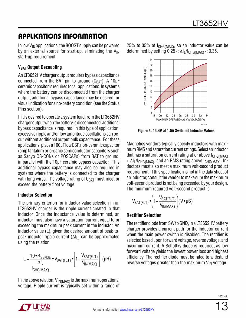
The primary criterion for inductor value selection in an LT3652HV charger is the ripple current created in that inductor. Once the inductance value is determined, an inductor must also have a saturation current equal to or exceeding the maximum peak current in the inductor. An inductor value (L), given the desired amount of peak-to-peak inductor ripple current (ΔIL) can be approximated using the relation:
L= 10 •RSENSEΔIL
ICHG(MAX)
• VBAT(FLT) • 1–VBAT(FLT)
VIN(MAX)
⎡
⎣⎢⎢
⎤
⎦⎥⎥� µH( )
In the above relation, VIN(MAX) is the maximum operational voltage. Ripple current is typically set within a range of
25% to 35% of ICHG(MAX), so an inductor value can be determined by setting 0.25 < ΔIL/ICHG(MAX) < 0.35.
Figure 3. 14.4V at 1.5A Switched Inductor Values
MAXIMUM OPERATIONAL VIN VOLTAGE (V)18 20 22
4
SWIT
CHED
INDU
CTOR
VAL
UE (µ
H)
12
10
14
24
16
18
20
22
34
3652 F03
8
6
26 2824 30 32
Magnetics vendors typically specify inductors with maxi-mum RMS and saturation current ratings. Select an inductor that has a saturation current rating at or above ICHG(MAX) + ∆IL/ICHG(MAX), and an RMS rating above ICHG(MAX). In-ductors must also meet a maximum volt-second product requirement. If this specification is not in the data sheet of an inductor, consult the vendor to make sure the maximum volt-second product is not being exceeded by your design. The minimum required volt-second product is:
VBAT(FLT) • 1−
VBAT(FLT)
VIN(MAX)
⎛
⎝⎜⎜
⎞
⎠⎟⎟ V •µS( )
Rectifier Selection
The rectifier diode from SW to GND, in a LT3652HV battery charger provides a current path for the inductor current when the main power switch is disabled. The rectifier is selected based upon forward voltage, reverse voltage, and maximum current. A Schottky diode is required, as low forward voltage yields the lowest power loss and highest efficiency. The rectifier diode must be rated to withstand reverse voltages greater than the maximum VIN voltage.

LT3652HV
143652hvfb
For more information www.linear.com/LT3652HV
APPLICATIONS INFORMATIONThe minimum average diode current rating (IDIODE(MAX)) is calculated with maximum output current (ICHG(MAX)), maximum operational VIN, and output at the precondition threshold (VBAT(PRE), or 0.7 • VBAT(FLT)):
IDIODE(MAX) >ICHG(MAX) •VIN(MAX) – VBAT(PRE)
VIN(MAX)(A)
For example, a rectifier diode for a 7.2V, 2A charger with a 25V maximum input voltage would require:
IDIODE(MAX) >2A • 25V−0.7(7.2V)
25V,or
IDIODE(MAX) >1.6A
Battery Float Voltage Programming
The output battery float voltage (VBAT(FLT)) is programmed by connecting a resistor divider from the BAT pin to VFB. VBAT(FLT) can be programmed up to 18V.
Figure 4. Feedback Resistors from BAT to VFB Program Float Voltage
BAT +
VFB
RFB2
RFB1LT3652HV
3652 F04
Because the battery voltage is across the VBAT(FLT) pro-gramming resistor divider, this divider will draw a small amount of current from the battery (IRFB) at a rate of:
IRFB = 3.3/RFB2
Precision resistors in high values may be hard to ob-tain, so for some lower VBAT(FLT) applications, it may be desirable to use smaller-value feedback resistors with an additional resistor (RFB3) to achieve the required 250k equivalent resistance. The resulting 3-resistor network, as shown in Figure 5, can ease component selection and/or increase output voltage precision, at the expense of additional current through the feedback divider.
For a three-resistor network, RFB1 and RFB2 follow the relation:
RFB2/RFB1 = 3.3/(VBAT(FLT) – 3.3)
Example:
For VBAT(FLT) = 3.6V:
RFB2/RFB1 = 3.3/(3.6 - 3.3) = 11.
Setting divider current (IRFB) = 10µA yields:
RFB2 = 3.3/10µA
RFB2 = 330k
Solving for RFB1:
RFB1 = 330k/11
RFB1 = 30k
The divider equivalent resistance is:
RFB1||RFB2 = 27.5k
BAT +
VFB
RFB2
RFB3RFB1
LT3652HV
3652 F05
Figure 5. A Three-Resistor Feedback Network Can Ease Component Selection
Using a resistor divider with an equivalent input resistance at the VFB pin of 250k compensates for input bias current error. Required resistor values to program desired VBAT(FLT) follow the equations:
RFB1 = (VBAT(FLT) • 2.5 • 105)/3.3 (Ω)
RFB2 = (RFB1 • (2.5 • 105))/(RFB1- (2.5 • 105)) (Ω)
The charge function operates to achieve the final float voltage of 3.3V on the VFB pin. The auto-restart feature initiates a new charging cycle when the voltage at the VFB pin falls 2.5% below that float voltage.

LT3652HV
153652hvfb
For more information www.linear.com/LT3652HV
To satisfy the 250k equivalent resistance to the VFB pin:
RFB3 = 250k − 27.5k
RFB3 = 223k.
Because the VFB pin is a relatively high impedance node, stray capacitances at this pin must be minimized. Spe-cial attention should be given to any stray capacitances that can couple external signals onto the pin, which can produce undesirable output transients or ripple. Effects of parasitic capacitance can typically be reduced by adding a small-value (20pF to 50pF) feedforward capacitor from the BAT pin to the VFB pin.
Extra care should be taken during board assembly. Small amounts of board contamination can lead to significant shifts in output voltage. Appropriate post-assembly board cleaning measures should be implemented to prevent board contamination, and low-leakage solder flux is recommended.
Input Supply Voltage Regulation
The LT3652HV contains a voltage monitor pin that enables programming a minimum operational voltage. Connect-ing a resistor divider from VIN to the VIN_REG pin enables programming of minimum input supply voltage, typically used to program the peak power voltage for a solar panel. Maximum charge current is reduced when the VIN_REG pin is below the regulation threshold of 2.7V.
If an input supply cannot provide enough power to satisfy the requirements of an LT3652HV charger, the supply volt-age will collapse. A minimum operating supply voltage can thus be programmed by monitoring the supply through a resistor divider, such that the desired minimum voltage corresponds to 2.7V at the VIN_REG pin. The LT3652HV servos the maximum output charge current to maintain the voltage on VIN_REG at or above 2.7V.
Programming of the desired minimum voltage is ac-complished by connecting a resistor divider as shown in Figure 6. The ratio of RIN1/RIN2 for a desired minimum voltage (VIN(MIN)) is:
RIN1/RIN2 = (VIN(MIN)/2.7) – 1
APPLICATIONS INFORMATIONIf the voltage regulation feature is not used, connect the VIN_REG pin to VIN.
MPPT Temperature Compensation
A typical solar panel is comprised of a number of series-con-nected cells, each cell being a forward-biased p-n junction. As such, the open-circuit voltage (VOC) of a solar cell has a temperature coefficient that is similar to a common p-n diode, or about –2mV/°C. The peak power point voltage (VMP) for a crystalline solar panel can be approximated as a fixed voltage below VOC, so the temperature coefficient for the peak power point is similar to that of VOC.
Panel manufacturers typically specify the 25°C values for VOC, VMP, and the temperature coefficient for VOC, making determination of the temperature coefficient for VMP of a typical panel straight forward.
The LT3652HV employs a feedback network to program the VIN input regulation voltage. Manipulation of the network makes for efficient implementation of various temperature compensation schemes for a maximum peak
Figure 6. Resistor Divider Sets Minimum VIN
VIN
VIN_REG
RIN2
RIN1 LT3652HV
INPUTSUPPLY
3652 F06
Figure 7. Temperature Characteristics for Solar Panel Output Voltage
TEMPERATURE (°C)5
PANE
L VO
LTAG
E (V
)
25 45 5515 35
3652 F07
VOC(25°C)
VMP(25°C)
VMP
VOC
VOC TEMP CO.
VOC – VMP

LT3652HV
163652hvfb
For more information www.linear.com/LT3652HV
power tracking (MPPT) application. As the temperature characteristic for a typical solar panel VMP voltage is highly linear, a simple solution for tracking that characteristic can be implemented using an LM234 3-terminal temperature sensor. This creates an easily programmable, linear tem-perature dependent characteristic.
In the circuit shown in figure 8,
APPLICATIONS INFORMATIONBattery Voltage Temperature Compensation
Some battery chemistries have charge voltage require-ments that vary with temperature. Lead-acid batteries in particular experience a significant change in charge volt-age requirements as temperature changes. For example, manufacturers of large lead-acid batteries recommend a float charge of 2.25V/cell at 25°C. This battery float voltage, however, has a temperature coefficient which is typically specified at –3.3mV/°C per cell.
In a manner similar to the MPPT temperature correction outlined previously, implementation of linear battery charge voltage temperature compensation can be ac-complished by incorporating an LM234 into the output feedback network.
For example, a 6-cell lead acid battery has a float charge voltage that is commonly specified at 2.25V/cell at 25°C, or 13.5V, and a –3.3mV/°C per cell temperature coefficient, or –19.8mV/°C. Using the feedback network shown in Figure 9, with the desired temperature coefficient (TC)
Figure 8. MPPT Temperature Compensation Network
VIN_REG
LT3652HV
VIN
VINLM234
3658 F08
V+
V–R
RSET
RIN1
RIN2
RIN1 = –RSET • (TC • 4405), and
RIN2 = RIN1/({[VMP(25°C) + RIN1 • (0.0674/RSET)]/VIN_REG} – 1)
Where: TC = temperature coefficient (in V/°C), and VMP(25°C) = maximum power voltage at 25°C
For example, given a common 36-cell solar panel that has the following specified characteristics:
Open Circuit Voltage (VOC) = 21.7V
Maximum Power Voltage (VMP) = 17.6V
Open-Circuit Voltage Temperature Coefficient (VOC) = –78mV/°C
As the temperature coefficient for VMP is similar to that of VOC, the specified temperature coefficient for VOC (TC) of –78mV/°C and the specified peak power voltage (VMP(25°C)) of 17.6V can be inserted into the equations to calculate the appropriate resistor values for the tempera-ture compensation network in Figure 8. With RSET equal to 1000Ω, then:
RSET = 1k
RIN1 = –1k • (–0.078 • 4405 ) = 344k
RIN2 = 344k/({[17.6 + 344k • (0.0674/1k)]/2.7} – 1) = 24.4k
LT3652HV
RFB3215k RFB2
43k
RSET2.4k
RFB1210k
6-CELLLEAD-ACID
BATTERY
LM234
3652 F09a
V+
V–R
BAT
VFB
+
Figure 9. Lead-Acid 6-Cell Float Charge Voltage vs Temperature Has –19.8mV/°C Characteristic Using LM234 with Feedback Network
TEMPERATURE (°C)–10
V FLO
AT (V
)
10 5040 600 20 30
3652 F09b
12.6
12.8
13.0
13.2
13.4
13.6
13.8
14.0
14.2
14.3
–19.8mV/°C

LT3652HV
173652hvfb
For more information www.linear.com/LT3652HV
APPLICATIONS INFORMATIONand 25°C float voltage (VFLOAT(25°C)) specified, and using a convenient value of 2.4k for RSET, necessary resistor values follow the relations:
RFB1 = –RSET • (TC • 4405)
= –2.4k • (–0.0198 • 4405) = 210k
RFB2 = RFB1/({[VFLOAT(25°C) + RFB1 • (0.0674/ RSET)] / VFB} – 1)
= 210k/({[13.5 + 210k • (0.0674/2.4k)]/3.3} – 1) = 43k
RFB3 = 250k - RFB1||RFB2
= 250k – 210k||43k = 215k (see the Battery Float Voltage Programming section)
While the circuit in Figure 9 creates a linear temperature characteristic that follows a typical –3.3mV/°C per cell lead-acid specification, the theoretical float charge voltage characteristic is slightly nonlinear. This nonlinear charac-teristic follows the relation VFLOAT(1-CELL) = 4 × 10⁻⁵ (T2) – 6 × 10⁻³(T) + 2.375 (with a 2.18V minimum), where T = temperature in °C. A thermistor-based network can be used to approximate the nonlinear ideal temperature characteristic across a reasonable operating range, as shown in Figure 10.
Status Pins
The LT3652HV reports charger status through two open collector outputs, the CHRG and FAULT pins. These pins can accept voltages as high as VIN, and can sink up to 10mA when enabled.
The CHRG pin indicates that the charger is delivering current at greater that a C/10 rate, or 1/10th of the pro-grammed maximum charge current. The FAULT pin signals bad battery and NTC faults. These pins are binary coded, and signal following the table below, where ON indicates pin pulled low, and OFF indicates pin high-impedance:
STATUS PINS STATE
CHARGER STATUSCHRG FAULT
OFF OFF Not Charging — Standby or Shutdown Mode
OFF ON Bad Battery Fault (Precondition Timeout / EOC Failure)
ON OFF Normal Charging at C/10 or Greater
ON ON NTC Fault (Pause)
If the battery is removed from an LT3652HV charger that is configured for C/10 termination, a sawtooth waveform
LT3652HV
196k
198k
6-CELLLEAD-ACID
BATTERY
22kB = 3380
3652 F10a
BAT
69k
69k
VFB
+
TEMPERATURE (°C)–10
V FLO
AT (V
)
10 5040 600 20 30
3652 F10b
12.8
13.0
13.2
13.4
13.6
13.8
14.0
14.6
14.4
14.2
14.8
THEORETICAL VFLOAT
PROGRAMMED VBAT(FLOAT)
Figure 10. Thermistor-Based Temperature Compensation Network Programs VFLOAT to Closely Match Ideal Lead-Acid Float Charge Voltage for 6-Cell Charger

LT3652HV
183652hvfb
For more information www.linear.com/LT3652HV
APPLICATIONS INFORMATIONof approximately 100mV appears at the charger output, due to cycling between termination and recharge events, This cycling results in pulsing at the CHRG output. An LED connected to this pin will exhibit a blinking pattern, indicating to the user that a battery is not present. The frequency of this blinking pattern is dependent on the output capacitance.
C/10 Termination
The LT3652HV supports a low-current based termination scheme, where a battery charge cycle terminates when the current output from the charger falls to below one-tenth of the maximum current, as programmed with RSENSE. The C/10 threshold current corresponds to 10mV across RSENSE. This termination mode is engaged by shorting the TIMER pin to ground.
When C/10 termination is used, a LT3652HV charger will source battery charge current as long as the average current level remains above the C/10 threshold. As the full-charge float voltage is achieved, the charge current falls until the C/10 threshold is reached, at which time the charger terminates and the LT3652HV enters standby mode. The CHRG status pin follows the charger cycle, and is high impedance when the charger is not actively charging.
When VBAT drops below 97.5% of the full-charged float voltage, whether by battery loading or replacement of the battery, the charger automatically re-engages and starts charging.
There is no provision for bad battery detection if C/10 termination is used.
Timer Termination
The LT3652HV supports a timer based termination scheme, in which a battery charge cycle is terminated after a specific amount of time elapses. Timer termination is engaged when a capacitor (CTIMER) is connected from the TIMER pin to ground. The timer cycle EOC (TEOC) occurs based
on CTIMER following the relation:
CTIMER = TEOC • 2.27 × 10⁻⁷ (Hours)
Timer EOC is typically set to 3 hours, which requires a 0.68µF capacitor.
The CHRG status pin continues to signal charging at a C/10 rate, regardless of what termination scheme is used. When timer termination is used, the CHRG status pin is pulled low during a charging cycle until the charger output current falls below the C/10 threshold. The charger continues to top-off the battery until timer EOC, when the LT3652HV terminates the charging cycle and enters standby mode.
Termination at the end of the timer cycle only occurs if the charging cycle was successful. A successful charge cycle is when the battery is charged to within 2.5% of the full-charge float voltage. If a charge cycle is not successful at EOC, the timer cycle resets and charging continues for another full timer cycle.
When VBAT drops below 97.5% of the full-charge float voltage, whether by battery loading or replacement of the battery, the charger automatically reengages and starts charging.
Preconditioning and Bad Battery Fault
A LT3652HV has a precondition mode, where charge cur-rent is limited to 15% of the programmed ICHG(MAX), as set by RSENSE. The precondition current corresponds to 15mV across RSENSE.
Precondition mode is engaged while the voltage on the VFB pin is below the precondition threshold (2.3V, or 0.7 • VBAT(FLT)). Once the VFB voltage rises above the precondition threshold, normal full-current charging can commence. The LT3652HV incorporates 70mV of threshold hysteresis to prevent mode glitching.

LT3652HV
193652hvfb
For more information www.linear.com/LT3652HV
When the internal timer is used for termination, bad battery detection is engaged. There is no provision for bad battery detection if C/10 termination is used. A bad battery fault is triggered when the voltage on VFB remains below the precondition threshold for greater than 1/8 of a full timer cycle (1/8 EOC). A bad battery fault is also triggered if a normally charging battery re-enters precondition mode after 1/8 EOC.
When a bad battery fault is triggered, the charging cycle is suspended, so the CHRG status pin becomes high-impedance. The FAULT pin is pulled low to signal a fault detection.
Cycling the charger’s power or SHDN function initiates a new charging cycle, but a LT3652HV charger does not require a reset. Once a bad battery fault is detected, a new timer charging cycle initiates when the VFB pin exceeds the precondition threshold voltage. During a bad battery fault, 0.5mA is sourced from the charger, so removing the failed battery allows the charger output voltage to rise and initi-ate a charge cycle reset. As such, removing a bad battery resets the LT3652HV, so a new charge cycle is started by connecting another battery to the charger output.
Battery Temperature Monitor and Fault
The LT3652HV can accommodate battery temperature monitoring by using an NTC (negative temperature co-effi-cient) thermistor close to the battery pack. The temperature monitoring function is enabled by connecting a 10kΩ, B = 3380 NTC thermistor from the NTC pin to ground. If the NTC function is not desired, leave the pin unconnected.
The NTC pin sources 50µA, and monitors the voltage dropped across the 10kΩ thermistor. When the voltage on this pin is above 1.36V (0°C) or below 0.29V (40°C), the battery temperature is out of range, and the LT3652HV triggers an NTC fault. The NTC fault condition remains until the voltage on the NTC pin corresponds to a temperature within the 0°C to 40°C range. Both hot and cold thresholds incorporate hysteresis that correspond to 5°C.
APPLICATIONS INFORMATIONIf higher operational charging temperatures are desired, the temperature range can be expanded by adding series resistance to the 10k NTC resistor. Adding a 0.91k resistor will increase the effective hot temperature to 45°C.
During an NTC fault, charging is halted and both status pins are pulled low. If timer termination is enabled, the timer count is suspended and held until the fault condi-tion is relieved.
Thermal Foldback
The LT3652HV contains a thermal foldback protection feature that reduces maximum charger output current if the IC junction temperature approaches 125°C. In most cases, on-chip temperatures servo such that any exces-sive temperature conditions are relieved with only slight reductions in maximum charger current.
In some cases, the thermal foldback protection feature can reduce charger currents below the C/10 threshold. In applications that use C/10 termination (TIMER = 0V), the LT3652HV will suspend charging and enter standby mode until the excessive temperature condition is relieved.
Layout Considerations
The LT3652HV switch node has rise and fall times that are typically less than 10nS to maximize conversion efficiency. The switch node (Pin SW) trace should be kept as short as possible to minimize high frequency noise. The input capacitor (CIN) should be placed close to the IC to minimize this switching noise. Short, wide traces on these nodes also help to avoid voltage stress from inductive ringing. The BOOST decoupling capacitor should also be in close proximity to the IC to minimize inductive ringing. The SENSE and BAT traces should be routed together, and these and the VFB trace should be kept as short as pos-sible. Shielding these signals from switching noise with a ground plane is recommended.

LT3652HV
203652hvfb
For more information www.linear.com/LT3652HV
APPLICATIONS INFORMATIONHigh current paths and transients should be kept iso-lated from battery ground, to assure an accurate output voltage reference. Effective grounding can be achieved by considering switched current in the ground plane, and careful component placement and orientation can effectively steer these high currents such that the battery reference does not get corrupted. Figure 11 illustrates an effective grounding scheme using component placement to control ground currents. When the switch is enabled (loop #1), current flows from the input bypass capacitor (CIN) through the switch and inductor to the battery posi-
SWVIN
RSENSE
SENSE
BAT
VFB
+GND
LT3652HV
DF
CIN CBAT VBAT
2
3652 F11
1
Figure 11. Component Orientation Isolates High Current Paths from Sensitive Nodes
tive terminal. When the switch is disabled (loop #2), the current to the battery positive terminal is provided from ground through the freewheeling Schottky diode (DF). In both cases, these switch currents return to ground via the output bypass capacitor (CBAT).
The LT3652HV packaging has been designed to efficiently remove heat from the IC via the Exposed Pad on the backside of the package, which is soldered to a copper footprint on the PCB. This footprint should be made as large as possible to reduce the thermal resistance of the IC case to ambient air.

LT3652HV
213652hvfb
For more information www.linear.com/LT3652HV
TYPICAL APPLICATIONS2A Solar Panel Power Manager With 7.2V LiFePO4 Battery
and 17V Peak Power TrackingSolar Panel Input Voltage Regulation,
Tracks Max Power Point to Greater Than 98%
SWVINVIN
6V TO 34V (40V MAX)
VIN_REG
VFB
BOOST
SENSE
BAT
NTC
TIMER
CMDSH2-4L
SYSTEMLOAD
1µF
30k
223k3652 TA05
+
10µF
C310µF
0.05
5.6µHLT3652HV
SHDN
CHRG
FAULT
CMSH3-40MACMSH3-40MA
330k
LiFePO4 CELL
Basic 2A 1-Cell LiFePO4 Charger (3.6V Float) with C/10 Termination
SWVIN
SOLAR PANEL INPUT
(<40V OC VOLTAGE)
VIN_REG
VFB
BOOST
SENSE
BAT
NTC
TIMER
CMSH3-40MASYSTEM LOAD
1µF
542k
459k
3652 TA02
10kB = 3380
2-CELL LiFePO4 (2 × 3.6V) BATTERY PACK
+
10µF
CMSH1-40MA
10µF
10µH
0.05
LT3652HV
530k
100k
SHDN
CHRG
FAULT
CMSH3-40MA
CHARGER OUTPUT CURRENT (A)0.2
INPU
T RE
GULA
TION
VOL
TAGE
(V)
10
12
14
20
18
16
0.6 1 1.2
3652 TA03
22
0.4 0.8 1.61.4 21.8
100% TO 98% PEAK POWER
98% TO 95% PEAK POWER
TA = 25°C

LT3652HV
223652hvfb
For more information www.linear.com/LT3652HV
3.00 ±0.10(4 SIDES)
NOTE:1. DRAWING IS NOT A JEDEC PACKAGE OUTLINE2. DRAWING NOT TO SCALE3. ALL DIMENSIONS ARE IN MILLIMETERS4. DIMENSIONS OF EXPOSED PAD ON BOTTOM OF PACKAGE DO NOT INCLUDE MOLD FLASH. MOLD FLASH, IF PRESENT, SHALL NOT EXCEED 0.15mm ON ANY SIDE5. EXPOSED PAD AND TIE BARS SHALL BE SOLDER PLATED6. SHADED AREA IS ONLY A REFERENCE FOR PIN 1 LOCATION ON THE TOP AND BOTTOM OF PACKAGE
0.40 ±0.10
BOTTOM VIEW—EXPOSED PAD
1.65 ±0.10
0.75 ±0.05
R = 0.115TYP
16
127
PIN 1TOP MARK
(SEE NOTE 6)
0.200 REF
0.00 – 0.05
(DD12) DFN 0106 REV A
0.23 ±0.05
PIN 1 NOTCHR = 0.20 OR0.25 × 45°CHAMFER
2.38 ±0.10
2.25 REF0.45 BSC
RECOMMENDED SOLDER PAD PITCH AND DIMENSIONSAPPLY SOLDER MASK TO AREAS THAT ARE NOT SOLDERED
0.25 ±0.05
2.25 REF
2.38 ±0.051.65 ±0.052.10 ±0.05
0.70 ±0.05
3.50 ±0.05
PACKAGEOUTLINE
0.45 BSC
DD Package12-Lead Plastic DFN (3mm × 3mm)
(Reference LTC DWG # 05-08-1725 Rev A)
Please refer to http://www.linear.com/product/LT3652HV#packaging for the most recent package drawings.
MSOP (MSE12) 0213 REV G
0.53 ±0.152(.021 ±.006)
SEATINGPLANE
0.18(.007)
1.10(.043)MAX
0.22 – 0.38(.009 – .015)
TYP
0.86(.034)REF
0.650(.0256)
BSC
12
12 11 10 9 8 7
7
DETAIL “B”
1 6
NOTE:1. DIMENSIONS IN MILLIMETER/(INCH)2. DRAWING NOT TO SCALE3. DIMENSION DOES NOT INCLUDE MOLD FLASH, PROTRUSIONS OR GATE BURRS. MOLD FLASH, PROTRUSIONS OR GATE BURRS SHALL NOT EXCEED 0.152mm (.006") PER SIDE4. DIMENSION DOES NOT INCLUDE INTERLEAD FLASH OR PROTRUSIONS. INTERLEAD FLASH OR PROTRUSIONS SHALL NOT EXCEED 0.152mm (.006") PER SIDE5. LEAD COPLANARITY (BOTTOM OF LEADS AFTER FORMING) SHALL BE 0.102mm (.004") MAX6. EXPOSED PAD DIMENSION DOES INCLUDE MOLD FLASH. MOLD FLASH ON E-PAD SHALL NOT EXCEED 0.254mm (.010") PER SIDE.
0.254(.010) 0° – 6° TYP
DETAIL “A”
DETAIL “A”
GAUGE PLANE
RECOMMENDED SOLDER PAD LAYOUT
BOTTOM VIEW OFEXPOSED PAD OPTION
2.845 ±0.102(.112 ±.004)2.845 ±0.102
(.112 ±.004)
4.039 ±0.102(.159 ±.004)
(NOTE 3)
1.651 ±0.102(.065 ±.004)
1.651 ±0.102(.065 ±.004)
0.1016 ±0.0508(.004 ±.002)
1 2 3 4 5 6
3.00 ±0.102(.118 ±.004)
(NOTE 4)
0.406 ±0.076(.016 ±.003)
REF
4.90 ±0.152(.193 ±.006)
DETAIL “B”CORNER TAIL IS PART OF
THE LEADFRAME FEATURE.FOR REFERENCE ONLY
NO MEASUREMENT PURPOSE
0.12 REF
0.35REF
5.10(.201)MIN
3.20 – 3.45(.126 – .136)
0.889 ±0.127(.035 ±.005)
0.42 ±0.038(.0165 ±.0015)
TYP
0.65(.0256)
BSC
MSE Package12-Lead Plastic MSOP, Exposed Die Pad
(Reference LTC DWG # 05-08-1666 Rev G)
PACKAGE DESCRIPTION

LT3652HV
233652hvfb
For more information www.linear.com/LT3652HV
Information furnished by Linear Technology Corporation is believed to be accurate and reliable. However, no responsibility is assumed for its use. Linear Technology Corporation makes no representa-tion that the interconnection of its circuits as described herein will not infringe on existing patent rights.
REVISION HISTORYREV DATE DESCRIPTION PAGE NUMBER
A 01/13 Added new Battery Bias Current curve 6
B 01/16 Enhanced Pin ConfigurationAdded Note 2 to top of Electrical CharacteristicsEnhanced Note 2Changed Name of Pin 13Modified Inductor Selection sectionModified Battery Float Voltage Programming Equations
23, 4
481315

LT3652HV
243652hvfb
For more information www.linear.com/LT3652HV LINEAR TECHNOLOGY CORPORATION 2010
LT 0116 REV B • PRINTED IN USALinear Technology Corporation1630 McCarthy Blvd., Milpitas, CA 95035-7417(408) 432-1900 ● FAX: (408) 434-0507 ● www.linear.com/LT3652HV
RELATED PARTS
TYPICAL APPLICATION1A Solar Panel Powered 3-Stage 12V Lead-Acid Fast/Float Charger; 1A Charger Fast Charges with CC/CV Characteristics Up to 14.4V; When Charge Current Falls to 0.1A Charger Switches to 13.5V Float Charge Mode; Charger Re-Initiates 14.4V Fast Charge Mode if Battery Voltage Falls Below 13.2V and Trickle Charges at 0.15A if Battery Voltage is Below 10V; 0°C to 45°C Battery Temperature Charging Range
SWVIN
SOLAR PANEL INPUT<40V OC VOLTAGE
16V PEAK POWER VOLTAGE
VIN_REG
VFB
BOOST
SENSEBAT
NTC
TIMER
22µH MBRS340
309k
100k
1µF 1N4148 BZX84C6V2L
910
174k
1N41481M
SYSTEMLOAD
WURTH7447779122
12V LEADACID BATTERY10k
B = 3380muRata
NCP18XH103
+
10µF
0.1
100µF
LT3652HV
10µF
4.7µF
SHDNCHRG
FAULT
499k
100k +
3652 TA04
MBRS140
PART NUMBER DESCRIPTION COMMENTS
LT3650-8.2/LT3650-8.4 Monolithic 2A Switch Mode 2-Cell Li-Ion Battery Charger
Standalone, 9V ≤ VIN ≤ 32V (40V Absolute Maximum), 1MHz, 2A Programmable Charge Current, Timer or C/10 Termination, Small and Few External Components, 3mm × 3mm DFN12 Package, –8.2 for 2 × 4.1V Float Voltage Batteries, –8.4 for 2 × 4.2V Float Voltage Batteries
LTC4001/LTC4001-1 Monolithic 2A Switch Mode Synchronous Li-Ion Battery Charger
Standalone, 4V ≤ VIN ≤ 5.5V (6V Absolute Maximum, 7V Transient), 1.5MHz, Synchronous Rectification Efficiency >90%, Adjustable Timer Termination, Small and Few External Components, 4mm × 4mm QFN-16 Package –1 for 4.1V Float Voltage Batteries
LTC4002 Switch Mode Lithium-Ion Battery Charger Standalone, 4.7V ≤ VIN ≤ 24V, 500kHz Frequency, 3 Hour Charge TerminationLTC4006 Small, High Efficiency, Fixed Voltage,
Lithium-Ion Battery Charger with Termination and Thermistor Sensor
Complete Charger for 3- or 4-Cell Li-Ion Batteries, AC Adapter Current Limit, 16-Pin Narrow SSOP Package
LTC4007 High Efficiency, Programmable Voltage Battery Charger with Termination
Complete Charger for 3- or 4-Cell Li-Ion Batteries, AC Adapter Current Limit, Thermistor Sensor and Indicator Outputs
LTC4008 4A, High Efficiency, Multi-Chemistry Battery Charger
Constant-Current/Constant-Voltage Switching Regulator Charger, Resistor Voltage/Current Programming, AC Adapter Current Limit and Thermistor Sensor and Indicator Outputs
LTC4012/LTC4012-1/ LTC4012-2/ LTC4012-3
4A, High Efficiency, Multi-Chemistry Battery Charger with PowerPath™ Control
PowerPath Control, Constant-Current/Constant-Voltage Switching Regulator Charger, Resistor Voltage/Current Programming, AC Adapter Current Limit and Thermistor Sensor and Indicator Outputs 1 to 4 Cell Li, Up to 18 Cell Ni, SLA and Supercap Compatible; 4mm × 4mm QFN-20 Package –1 Version for 4.1V Li Cells, –2 Version for 4.2V Li Cells, –3 Version has Extra GND Pin
LTC4015 Multichemistry Buck Battery Charger Controller with Digital Telemetry System
Multichemistry Li-Ion/Polymer, LiFePO4, or Lead-Acid Battery Charger with Termination, Digital Telemetry System Monitors VBAT, IBAT, RBAT, NTC Ratio (Battery Temperature), VIN, IIN, VSYSTEM, Die Temperature, Coulomb Counter and Integrated 14-Bit ADC, Maximum Power Point Tracking, Wide Charging Input Voltage Range: 4.5V to 35V, Wide Battery Voltage Range: Up to 35V, 5mm × 7mm QFN-38 Package
LTC4020 55V Buck-Boost Multi-Chemistry Battery Charger
Wide Voltage Range: 4.5V to 55V Input, Up to 55V Output (60V Absolute Maximums), Synchronous Buck-Boost DC/DC Controller, Li-Ion and Lead-Acid Charge Algorithms, Input Voltage Regulation for High Impedance Input Supplies and Solar Panel Peak Power Operation, Low Profile (0.75mm) 38-Pin 5mm × 7mm QFN Package


![Fonte estabilizada [0-40V x 5A].pdf](https://img.pdfslide.net/doc/110x75/577c77441a28abe0548b6581/fonte-estabilizada-0-40v-x-5apdf.jpg)


![Fonte Estabilizada [0-40V x 5A]](https://img.pdfslide.net/doc/110x75/5695d1d51a28ab9b02981a1a/fonte-estabilizada-0-40v-x-5a.jpg)

