Embed Size (px)
Citation preview
For more information www.linear.com/LT3697
LT3697
13697f
Typical applicaTion
FeaTures DescripTion
USB 5V, 2.5A Output, 35V Input Buck with
Cable Drop Compensation
The LT®3697 is a 35V, 2.5A step-down switching regulator designed to power 5V USB applications. A precise output voltage and programmable cable drop compensation maintain accurate 5V regulation at the USB socket connected to the end of a long cable. The accurate, programmable current limit can eliminate the need for a USB power switch and improve system reliability. The provided 180mA active load reduces output overshoot during load transients. Dual feedback allows regulation on the output of a USB switch and limits cable drop compensation to a maximum of 6.1V output, protecting USB devices during fault conditions. A separate 5V output can be taken from the SYS terminal to power auxiliary circuitry such as a USB hub controller. The LT3697 also provides a load current monitor output and an overcurrent fault indicator.
The LT3697 operates from 300kHz to 2.2MHz and with-stands input voltage transients up to 60V. The device's output survives shorts to ground and to the battery. A current mode topology is used for fast transient response and good loop stability. Shutdown reduces input supply current to less than 1µA. The LT3697 is available in a 16-lead MSOP package with an exposed pad for low thermal resistance.
5V Step-Down Converter with Cable Drop Compensation and Output Current Limit Transient Response
applicaTions
n Accurate 5V Outputn Programmable Cable Drop Compensationn Programmable Output Current Limitn Adjustable Output from 5.0V to 6.1Vn Dual Input Feedback Permits Regulation on Output
of USB Switchn Active Load Reduces Output Overshootn FLT Flag Indicates Overcurrent on the USB Outputn 1.5ms FLT Flag Delay Filters Hot Plug Eventsn USB Output Current Monitorn Wide Input Rage: Operation from 5V to 35Vn Withstands Input Transient to 60Vn 2.5A Maximum Output Currentn Survives Output Short to GND and Car Batteryn Adjustable Switching Frequency: 300kHz to 2.2MHzn Synchronizable from 300kHz to 2.2MHzn Small, Thermally Enhanced 16-Lead MSOP Package
n Automotive USBn Industrial USB
L, LT, LTC, LTM, Burst Mode, Linear Technology and the Linear logo are registered trademarks of Linear Technology Corporation. All other trademarks are the property of their respective owners.
0.022Ω 0.13Ω
10µH
10µFVIN BST
LT3697
EN SW
SYSISPISN
USB5VRCBL
FLTRTVCRLIMSYNC
GND330pF 1nF
1µF
47µF 10k10nF
VIN 6V TO 35VTRANSIENT TO 60V VOUT
0.13Ω
255k
16.5k 100µF
3697 TA01
4 METERS AWG 20TWISTED PAIR CABLE
VLOAD5V, 2.5ALO
AD
–
+
7.5k
+
250µs/DIV3697 TA01a
5.75
5.50
5.25
5.00
4.75
4.50
VOLT
AGE
(V)
6.0
5.0
4.0
3.0
2.0
1.0
CURRENT (A)
ILOAD25mA/µs
VLOAD
VOUT
For more information www.linear.com/LT3697
LT3697
23697f
pin conFiguraTionabsoluTe MaxiMuM raTings
VIN, EN Voltage (Note 2) ..........................................60VBST Voltage ..............................................................55VBST Above SW Voltage .............................................25VSYNC Voltage ..............................................................6VRT, VC, RLIM, RCBL Voltage .......................................3VFLT, ISN, ISP, USB5V, SYS Voltage ............................30VOperating Junction Temperature Range LT3697E ............................................ –40°C to 125°C LT3697I ............................................. –40°C to 125°CStorage Temperature Range .................. –65°C to 150°CLead Temperature (Soldering, 10sec).................... 300°C
(Note 1)
12345678
VINVINENFLT
SYNCRTVC
RLIM
161514131211109
SWSWBSTSYSUSB5VISPISNRCBL
TOP VIEW
MSE PACKAGE16-LEAD PLASTIC MSOP
17GND
θJA = 40°C/W
EXPOSED PAD (PIN 17) IS GND, MUST BE SOLDERED TO PCB
orDer inForMaTionLEAD FREE FINISH TAPE AND REEL PART MARKING* PACKAGE DESCRIPTION TEMPERATURE RANGE
LT3697EMSE#PBF LT3697EMSE#TRPBF 3697 16-Lead Plastic MSOP –40°C to 125°C
LT3697IMSE#PBF LT3697IMSE#TRPBF 3697 16-Lead Plastic MSOP –40°C to 125°C
Consult LTC Marketing for parts specified with wider operating temperature ranges. *The temperature grade is identified by a label on the shipping container.For more information on lead free part marking, go to: http://www.linear.com/leadfree/ For more information on tape and reel specifications, go to: http://www.linear.com/tapeandreel/
For more information www.linear.com/LT3697
LT3697
33697f
elecTrical characTerisTics
PARAMETER CONDITIONS MIN TYP MAX UNITS
VIN Undervoltage Lockout l 4.2 4.8 V
VIN Overvoltage Lockout l 35.5 37 39.5 V
Dropout Comparator Threshold (VIN – VSYS) Falling, VIN = 5V 550 650 750 mV
Dropout Comparator Hysteresis 200 mV
VIN Current VSYS = 5V, VEN = 0.3V VSYS = 5V, Not Switching VSYS = 0V, Not Switching
0.5 0.8
0.01 0.75 1.1
2 1.0 1.4
μA mA mA
SYS Current VEN = 0.3V VSYS = 5V, Not Switching VSYS = 0V, Not Switching
200
9 300 –75
13 500
–120
μA μA μA
USB5V Voltage l 4.95 4.99 5.03 V
USB5V Line Regulation 6V < VIN < 35V l 1 5 mV
USB5V Current VSENSE = 50mV, RCBL = 16.5k VSENSE = 10mV, RCBL = 16.5k VSENSE = 0V, RCBL = 16.5k
l
l
l
58 11
60 13 0
62 15 3
μA μA μA
RCBL Voltage VSENSE = 50mV, RCBL = 16.5k VSENSE = 10mV, RCBL = 16.5k VSENSE = 0V, RCBL = 16.5k
960 180
1000 210 0
1030 240 50
mV mV mV
RCBL Current Limit VRCBL = 0V, VSENSE = 50mV 200 300 400 μA
SYS Voltage VUSB5V = 0V l 6.0 6.1 6.2 V
SYS Voltage to Disable Switching VUSB5V = 0V 6.5 6.8 7.1 V
SENSE Voltage (Note 7) VISP = 5V, RLIM = Open VISP = 0V, RLIM = Open VISP = 5V, RLIM = 56.2k VISP = 5V, RLIM = 29.4k
l
l
l
l
56.5 20 33 18
60.5
35.2 20.5
64.5 105 37.5 23
mV mV mV mV
ISP and ISN Bias Current VISP, VISN = 5V VISP, VISN = 0V
20 –1.1
30 –1.6
μA mA
RLIM Current VRLIM = 1.2V –9 –11 –13 μA
Active Load Current from SYS VSYS = 5V 120 180 240 mA
USB5V Voltage Offset to Enable Active Load VUSB5V Rising 0.5 1.5 3 %
SYS Voltage Threshold to Disable Active Load VSYS Rising 6.6 7.2 7.8 V
Error Amp gm 400 mS
Error Amp Gain 500 V/V
VC Source Current VVC = 1.3V –80 μA
VC Sink Current VVC = 1.3V 80 μA
VC to Switch gm 5 A/V
VC Clamp Voltage 1.8 V
The l denotes the specifications which apply over the full operating temperature range, otherwise specifications are at TA = 25°C. VIN = 12V, VEN = 12V unless otherwise noted. (Notes 3, 6)
For more information www.linear.com/LT3697
LT3697
43697f
PARAMETER CONDITIONS MIN TYP MAX UNITS
Switching Frequency RT = 22.1k RT = 63.4k RT = 453k
l
l
l
1.8 0.9 250
2 1
300
2.25 1.12 350
MHz MHz KHZ
Foldback Frequency RT = 63.4k, VSYS = 0V 240 kHz
Minimum Switch On-Time ISW = 0.9A 100 160 ns
Minimum Switch Off-Time ISW = 0.9A 140 210 ns
Switch Current Limit (Note 8) l 4.3 5.3 6.7 A
Switch VCESAT ISW = 2A 220 mV
SW Leakage Current VEN = 0.3V, VBST = 5V, VSW = 0V 0.1 1 µA
Minimum BST Voltage (Note 9) ISW = 2A 1.6 2.2 V
BST Current ISW = 2A 35 65 mA
EN Input Voltage High l 2.5 V
EN Input Voltage Low l 0.3 V
EN Current VEN = 2.5V 1 2 μA
SENSE Voltage to Trigger FLT Percentage of Nominal Sense Voltage 97 99.5 100 %
FLT Blanking 0.5 1.5 4 ms
FLT Leakage VFLT = 5V 0.1 1 μA
FLT Sink Current VFLT = 0.3V l 100 180 μA
SYNC Threshold l 0.4 0.7 1 V
SYNC Current VSYNC = 5V 0.1 μA
elecTrical characTerisTics
Note 1: Stresses beyond those listed under Absolute Maximum Ratings may cause permanent damage to the device. Exposure to any Absolute Maximum Rating condition for extended periods may affect device reliability and lifetime.Note 2: Absolute maximum voltage at VIN and EN is 60V for nonrepetitive 1 second transients, and 35V for continuous operation.Note 3: The LT3697E is guaranteed to meet performance specifications from 0°C to 125°C junction temperature. Specifications over the –40°C to 125°C operating junction temperature range are assured by design, characterization and correlation with statistical process controls. The LT3697I is guaranteed over the full –40°C to 125°C operating junction temperature range. High junction temperatures degrade operating lifetimes. Operating lifetime is derated at junction temperatures greater than 125°C.Note 4: Note that the maximum ambient temperature consistent with these specifications is determined by specific operating conditions in conjunction with board layout, the rated package thermal impedance and other environmental factors.Note 5: This IC includes overtemperature protection that is intended
The l denotes the specifications which apply over the full operating temperature range, otherwise specifications are at TA = 25°C. VIN = 12V, VEN = 12V unless otherwise noted. (Notes 3, 6)
to protect the device during momentary overload conditions. Junction temperature will exceed 150°C when overtemperature protection is active. Continuous operation above the specified maximum operating junction temperature may impair device reliability.Note 6: Polarity specification for current into a pin is positive and out of a pin is negative. All voltages are referenced to GND unless otherwise specified. MAX and MIN refer to absolute values.Note 7: SENSE Voltage is defined as the differential voltage applied across the sense amplifier inputs, or VISP – VISN. SENSE voltage and VSENSE are synonymous.Note 8: Switch current limit is guaranteed by design and/or correlation to static test. Slope compensation reduces switch current limit at higher duty cycles.Note 9: Boost voltage is the minimum voltage across the boost capacitor needed to guarantee full saturation of the switch.
For more information www.linear.com/LT3697
LT3697
53697f
Typical perForMance characTerisTics
Output Current Limit Load LineSense Voltage (VISP - VISN) at 4.5V Output
Sense Voltage (VISP - VISN) at 0.5V Output Efficiency at 2MHz Efficiency at 400kHz
USB5V Voltage USB5V Voltage USB5V Current
USB5V Current
TEMPERATURE (°C)–50
4.95
V USB
5V (V
)
5.01
5.00
4.99
4.98
4.97
4.96
5.02
75 100 125 150–25 0 25
3697 G01
50
VIN = 12VILOAD = 1A
TEMPERATURE (°C)–50
0
I USB
5V (µ
A)
50
40
30
20
10
60
75 100 125 150–25 0 25
3697 G03
50
RCBL = 16.5kVSENSE = 40mV
VSENSE = 10mV
VSENSE = 0mV
VSENSE (mV)0
0
I USB
5V (µ
A)
250
200
150
100
50
300
40 50 60 7010 20
3697 G04
30
RCBL = 2k
RCBL = 16.5k
RCBL = 130k
OUTPUT CURRENT (A)0.0
0
OUTP
UT V
OLTA
GE (V
)
5
4
3
2
1
6
1.5 2.0 2.5 3.00.5
3697 G05
1.0
RLIM = 29.4kRLIM = 49.9k
RLIM = 75kRLIM = ∞
VIN = 12VRSENSE = 25mΩRCBL = ∞
TEMPERATURE (°C)–50
0
V ISP
- V I
SN (m
V)
50
60
40
30
20
10
70
50 10075 125 150–25
3697 G06
250
RLIM = 29.4k
RLIM = 0Ω
RLIM = 75k
RLIM = ∞
VIN = 12VVOUT = 4.5V
TEMPERATURE (°C)–50
0
V ISP
- V I
SN (m
V) 50
60
70
40
30
20
10
80
50 10075 125 150–25
3697 G07
250
RLIM = 29.4k
RLIM = 0Ω
RLIM = 75k
RLIM = ∞
VIN = 12VVOUT = 0.5V
INPUT VOLTAGE (V)6
4.96
USB5
V VO
LTAG
E (V
)
5.03
5.02
5.01
5.00
4.99
4.98
4.97
5.04
30 34 38 4210 1814 22
3697 G02
26
ILOAD = 1A
LOAD CURRENT (A)0.0
50
EFFI
CIEN
CY (%
)
80
90
70
60
100
1.0 1.5 2.0 2.5
3697 G08
0.5
fSW = 2MHzRSENSE = 22mΩL = 1.8µHDCRL = 10mΩRCBL = ∞
VIN = 16VVIN = 12VVIN = 8V
LOAD CURRENT (A)0.0
50
EFFI
CIEN
CY (%
)
80
90
70
60
100
1.0 1.5 2.0 2.5
3697 G09
0.5
fSW = 400kHzRSENSE = 22mΩL = 8.2µHDCRL = 24mΩRCBL = ∞
VIN = 24VVIN = 12VVIN = 8V
TA = 25°C, unless otherwise noted.
For more information www.linear.com/LT3697
LT3697
63697f
Typical perForMance characTerisTics
SYS Pin CurrentLT3697 Temperature RiseNo Load Input Current vs Input Voltage
No Load Input Current vs Temperature Switch VCESAT BST Pin Current
Switch Current Limit vs Temperature
Switch Current Limit vs Duty Cycle Switching Frequency
TA = 25°C, unless otherwise noted.
VSYS (V)0
0
I SYS
(mA)
160
120
80
40
200
5 6 7 81 2 3
3697 G11
4
VUSB5V = 5.5V
INPUT VOLTAGE (V)5
0.0
INPU
T CU
RREN
T (m
A)
2.5
2.0
1.5
1.0
0.5
3.0
25 30 35 4010 15
3697 G12
20
IN REGULATION
TEMPERATURE (°C)–50
0
NO L
OAD
INPU
T CU
RREN
T (m
A) 20
15
10
5
25
75 100 125 150–25 250
3697 G13
50
INCREASED SUPPLY CURRENTDUE TO CATCH DIODELEAKAGE AT HIGHTEMPERATURE
VIN = 12V CATCH DIODE:CENTRAL SEMICMSH3-40MA
SWITCH CURRENT (A)0.0
0
SWIT
CH V
CESA
T (m
V)
250
200
150
100
50
300
2.0 2.50.5 1.0
3697 G14
1.5
VBST - VSW = 4.5V
SWITCH CURRENT (A)0.0
0
BST
CURR
ENT
(mA)
40
30
20
10
50
2.0 2.50.5 1.0
3697 G15
1.5
VBST - VSW = 4.5V
TEMPERATURE (°C)–50
2.0
SWIT
CH C
URRE
NT L
IMIT
(A) 6.0
5.0
4.0
3.0
7.0
125 15050250–25 75
3697 G16
100
30% DC
70% DC
DUTY CYCLE (%)0
2
CURR
ENT
LIM
IT (A
)
6
5
4
3
7
80 10020 40
3697 G17
60TEMPERATURE (°C)
–50300
325
350
375
400
425
450
475
SWIT
CHIN
G FR
EQUE
NCY
(kHz
)
500
125 15050250–25 75
3697 G18
100
RT = 255k
OUTPUT CURRENT (A)0
0
IC T
EMPE
RATU
RE R
ISE
(°C)
40
30
20
10
2.510.5 1.5
3697 G10
2
DC1893A DEMO BOARD24°C AMBIENT TEMPERATURENO AIR FLOWfSW = 500kHz
VIN = 16VVIN = 12VVIN = 8V
For more information www.linear.com/LT3697
LT3697
73697f
Typical perForMance characTerisTics
Frequency Foldback
Minimum On-Time
Start-Up/Dropout Performance Start-Up/Dropout Performance
Minimum Off-Time Minimum Off-Time in SYNC
Enable Threshold
Burst Frequency Error Amp Output Current
TA = 25°C, unless otherwise noted.
VSYS (V)0
150
200
250
300
350
400
SWIT
CHIN
G FR
EQUE
NCY
(kHz
)
450
5 621 3
3697 G19
4
RT = 255k
LOAD CURRENT (mA)0
0
SWIT
CHIN
G FR
EQUE
NCY
(kHz
)
500
450
400
350
300
250
200
150
100
50
140 160604020 10080
3697 G20
120
RT = 255kL = 8.2µH
VIN = 36VVIN = 24VVIN = 12V
TEMPERATURE (°C)–50
80
MIN
IMUM
ON-
TIM
E (n
s)
160
140
120
100
180
125 15050250–25 75
3697 G22
100
0.9A LOAD
2.1A LOAD
TEMPERATURE (°C)–50
130
MIN
IMUM
OFF
-TIM
E (n
s) 160
150
140
170
125 15050250–25 75
3697 G23
100
2.1A LOAD
0.9A LOAD
TEMPERATURE (°C)–50
0.80
EN P
IN V
OLTA
GE (V
)
2.00
1.80
1.60
1.40
1.20
1.00
125 150250–25 7550
3697 G25
100
EN FALLINGEN RISING
100ms/DIV
2V/DIV
RLOAD = 2Ω(2.5A IN REGULATION)RCBL = ∞
3697 G26
VIN
VOUT
RLOAD = 100Ω(50mA IN REGULATION)RCBL = ∞
100ms/DIV
2V/DIV
3697 G27
VIN
VOUT
OFFSET FROM NOMINAL USB5V VOLTAGE (mV)–200
–100
VC P
IN C
URRE
NT (µ
A)
100
75
50
25
0
–25
–50
–75
200–100 0
3697 G21
100
TEMPERATURE (°C)–50
140
MIN
IMUM
OFF
-TIM
E (n
s) 200
190
180
170
160
150
220
210
125 15050250–25 75
3697 G24
100
2.1A LOAD
0.9A LOAD
FSYNC = 2.2MHz
For more information www.linear.com/LT3697
LT3697
83697f
Typical perForMance characTerisTics
Load Transient Response Through Cable
Load Transient Response Through Cable
Output Current Limit Transient Response
Feedback Shorted to Ground FLT DeglitchingRSENSE = 22mΩRLIM = OPEN
ILOAD
VFLT
2ms/DIV
0
FLT
VOLT
AGE
(V)
7
6
5
4
3
2
1
8
0.0
LOAD CURRENT (A)
0.5
1.0
1.5
2.0
2.5
3.0
3.5
4.0
3697 G33
200µs/DIV
FRONT PAGE CIRCUITVIN = 12VCABLE = 4m AWG20CLOAD = 10µF
VOUT
VLOAD
ILOAD25mA/µs
4.00
VOLT
AGE
(V) CURRENT (A)
5.75
5.50
5.25
5.00
4.75
4.50
4.25
0.0
7.0
6.0
5.0
4.0
3.0
2.0
1.0
3697 G30
200µs/DIV
FRONT PAGE CIRCUITVIN = 12VCABLE = 4m AWG20CLOAD = 10µF
VOUT
VLOAD
ILOAD25mA/µs
4.00
VOLT
AGE
(V) CURRENT (A)
5.75
5.50
5.25
5.00
4.75
4.50
4.25
0.0
7.0
6.0
5.0
4.0
3.0
2.0
1.0
3697 G29
1ms/DIV
VLOAD
ILOAD
VFLT
0
VOLT
AGE
(V) CURRENT (A)
6
5
4
3
2
1
0
12
10
8
6
4
2
3697 G31
FRONT PAGE CIRCUITVIN = 12V
200µs/DIV
VOUT
VUSB5V SHORTEDTO GROUND
VUSB5V
0.0
VOLT
AGE
(V)
7.0
6.0
5.0
4.0
3.0
2.0
1.0
3697 G32
Minimum Input Voltage
LOAD CURRENT (mA)
RSENSE = 22mΩRCBL = ∞RESISTOR LOADDCRL = 10mΩ
14.0
MIN
IMUM
INPU
T VO
LTAG
E (V
)
7.0
6.5
6.0
5.5
5.0
4.5
1000010 100
3697 G28
1000
VOLTAGE TO RUNVOLTAGE TO START
TA = 25°C, unless otherwise noted.
For more information www.linear.com/LT3697
LT3697
93697f
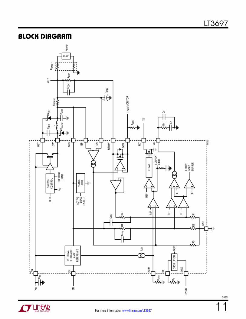
pin FuncTionsVIN (Pins 1, 2): The VIN pins supply current to the LT3697’s internal regulator and to the power switch. These pins must be locally bypassed.
EN (Pin 3): The EN pin is used to put the LT3697 into shutdown mode. Tie to ground to shut down the LT3697. Tie to 2.5V or higher for normal operation. If the shutdown feature is not used, tie this pin to the VIN pin.
FLT (Pin 4): The FLT pin is the open drain output of the LT3697 fault comparator and timer. In normal operation the FLT pin is high impedance. An overcurrent fault that is sustained for at least 1.5ms causes the LT3697 to pull the FLT pin low. The FLT pin then remains low until the USB output current stays below the overcurrent threshold for at least 1.5ms. The overcurrent fault threshold is 0.5% below the current limit. The FLT output is valid when VIN is above 4V and EN is high.
SYNC (Pin 5): The SYNC pin is the external clock synchro-nization input. Tie to a clock source with on and off times greater than 50ns for synchronization. Tie pin to ground if not used. See the Synchronization section in Applications Information for more details.
RT (Pin 6): The RT pin is the oscillator resistor input. Connect a resistor from this pin to ground to set the switching frequency.
VC (Pin 7): The VC pin is the output of the internal error amplifier. The voltage on this pin controls the peak switch current. Tie an R-C network from this pin to ground to compensate the control loop.
RLIM (Pin 8): The RLIM pin provides an additional reference to the third feedback amplifier of the LT3697 to allow the output current limit to be programmed easily. The RLIM pin has an accurate 11μA pull-up current. When the voltage of the output current sense amplifier exceeds the lower of the RLIM voltage or 1.22V, the LT3697 error amplifier will switch to current limit mode and will regulate the USB output current. In current limit mode, the output voltage drops. Tie a resistor from RLIM to ground to program the LT3697 current limit. If the USB output current exceeds
99.5% of the current limit for at least 1.5ms, the LT3697 will pull down on the FLT pin. Float the RLIM pin if not used.
RCBL (Pin 9): The RCBL pin is used to program the USB5V current as a function of sense voltage (VISP – VISN) for cable drop compensation. Tie a resistor from RCBL to ground to set the USB5V input current. Float the RCBL pin if cable drop compensation is not desired. The RCBL pin may also be used as an USB output current monitor. Excessive capacitive loading on the RCBL pin can cause USB output voltage overshoot during load steps when cable drop compensation is used. Keep the capacitive loading on the RCBL pin below 100pF.
ISN (PIN 10): The ISN pin is the inverting input of the LT3697’s onboard USB output current sense amplifier. Tie a resistor RSENSE from ISP to ISN to sense the USB output current. Connect ISN to ISP if the current monitor, USB output current limit, and cable drop compensation functions are not desired.
ISP (Pin 11): The ISP pin is the noninverting input of the LT3697’s onboard USB output current sense amplifier. Tie a resistor RSENSE from ISP to ISN to sense the USB output current. When a USB switch is used in series between the LT3697 and the 5V USB output, tie the ISP pin to the USB switch output.
USB5V (Pin 12): The USB5V pin is the primary feedback input of the internal error amplifier. In normal operation, the LT3697 regulates the voltage on this pin to 5V. The USB5V pin also allows the output voltage to increase as a function of output current to compensate for voltage drop at the point of load due to cable impedance. The USB5V pin input current is proportional to USB output current and is programmed by the RCBL resistor. Tie a resistor from USB5V to the 5V USB output to set this cable drop compensation.
Tie USB5V directly to the USB output if no cable drop compensation is desired. If a USB switch is used in se-ries between the LT3697 and the 5V USB output, tie the USB5V pin through the compensation resistor to the USB switch output.
For more information www.linear.com/LT3697
LT3697
103697f
pin FuncTionsSYS (Pin 13): The SYS pin is the second feedback input of the internal error amplifier. The SYS pin allows the LT3697 to regulate the output voltage at the output of a USB switch. If the USB switch goes open and the USB5V pin is no longer part of the control loop, the LT3697 regulates the SYS pin to 6.1V to protect the input of a USB switch from an overvoltage condition. The SYS pin also supplies current to the internal regulator of the LT3697 and may be used to supply power to auxiliary circuitry. The active load also draws current from this pin to reduce output overshoot. This pin must be locally bypassed and must be tied to the switching regulator output.
BST (Pin 14): The BST pin is used to provide a drive voltage, higher than the input voltage, to the internal NPN power switch.
SW (Pin 15, 16): The SW pins are the output of the internal power switch. Connect these pins to the inductor, catch diode, and boost capacitor.
GND (Pin 17): Ground. The exposed pad must be soldered to the PCB.
For more information www.linear.com/LT3697
LT3697
113697f
block DiagraM
R LIM
R T
CURR
ENT
LIM
IT
ACTI
VELO
ADEN
ABLE
R C
C C
C F
SWIT
CHCO
NTRO
LOS
C
CURR
ENT
LIM
IT
+–
+–
+ –
+–
+ –
+–
+–++–
++–
R5
R4R2
R3R1RE
F
REF
REF
REF RE
F
REF
C FF1
C FF2
V IN
V IN
ENEN
11µA
RLIM
C IN
RT SYNC
SYNC
INTE
RNAL
REGU
LATO
RAN
DRE
FERE
NCE
OSCI
LLAT
OROS
C
GND
VC
R CBL
I LOA
D M
ONIT
OR
RCBL
USB5
V
ISN
ISP
FLT
FLT
DELA
Y
SYS
SWBST
ACTI
VELO
AD
ACTI
VELO
ADEN
ABLE
V CD C
ATCH
C BST
C OUT
C CDC
C BUS
D BST
R SEN
SER C
ABLE
V LOA
DR C
DC
OUT
L
LOAD+ –
+
3697
BD

For more information www.linear.com/LT3697
LT3697
123697f
operaTionThe LT3697 is a constant frequency, current mode step-down regulator. The oscillator sets an RS flip-flop, turning on the internal power switch. The RT resistor sets the oscil-lator frequency. An amplifier and comparator monitor the current flowing between the VIN and SW pins, turning the switch off when this current reaches a level determined by the voltage at VC. The error amplifier measures the output voltage on the USB5V pin through an internal resistor di-vider and servos the VC node to regulate the USB5V pin to 5V. If the error amplifier’s output increases, more current is delivered to the output; if it decreases, less current is delivered. An active clamp on the VC pin provides switch peak current limit. The LT3697 can provide up to 2.5A of output current.
A second error amp input on the SYS pin allows a switch to be placed in the output path before the USB5V connection. SYS is regulated to 6.1V if this switch is open. A third error amp input is connected to the ISP and ISN pins through the internal current sense amplifier. The LT3697 regulates VSENSE voltage (VISP – VISN) to the lower of V(RLIM)/19.8 or 1.22V/19.8 to provide accurate output current limit.
To implement cable drop compensation, the LT3697 drives the RCBL pin to 19.8 (VISP – VISN). Current sourced from the RCBL pin is derived from the USB5V pin, creating an output offset above the 5V USB5V pin voltage that is proportional to the load current and the RCDC/RCBL resistor ratio.
The LT3697 includes a 180mA active load that sinks current from the SYS pin to ground. The purpose of this active load is to improve load step transient response and to charge the boost cap during startup. If USB5V is 1.5% above its nominal 5V output or if the boost drive voltage (VBST – VSW) is insufficient to fully saturate the internal NPN power switch, the active load is enabled.
An internal regulator provides power to the control circuitry. The bias regulator normally draws power from the VIN pin, but if the SYS pin is connected to an external voltage higher than 4V, some bias power will be drawn from the output voltage improving efficiency.
If the EN pin is low, the LT3697 is shut down and draws <1µA from the input. When the EN pin falls below 0.3V, the
switching regulator will shut down, and when the EN pin rises above 2.5V, the switching regulator will become active.
The switch driver operates from either VIN or from the BST pin. An external capacitor is used to generate a voltage at the BST pin that is higher than the input supply. This allows the driver to fully saturate the internal NPN power switch for efficient operation.
To further optimize efficiency, the LT3697 automatically switches to Burst Mode operation in light load situations. Between bursts, all circuitry associated with controlling the output switch is shut down, reducing the input supply current to 1mA.
The LT3697 has several features designed to enhance system robustness. The oscillator reduces the LT3697’s operating frequency when the voltage at the SYS pin is low. This frequency foldback helps to control the output current during startup and overload. A fast overcurrent compara-tor disables switching within one cycle if VSENSE exceeds 70mV, providing overcurrent protection that is faster than the current limit provided by the error amplifier. An overvolt-age comparator on the SYS pin disables switching within one cycle if VSYS exceeds 6.8V. Lastly, thermal shutdown protects the part from excessive power dissipation.
If the input voltage decreases towards the SYS output voltage, the LT3697 will start to skip switch-off times and decrease the switching frequency to maintain output regulation. As the input voltage decreases below the SYS output voltage, the SYS voltage will be regulated 600mV below the input voltage. This enforced minimum dropout voltage limits the duty cycle and keeps the boost capacitor charged during dropout conditions. Since sufficient boost voltage is maintained, the internal switch can fully saturate, resulting in good dropout performance.
The LT3697 contains fault logic that detects if the output current is near or exceeds the programmed current limit. If such a condition is maintained for >1.5ms, the FLT pin pulls low, indicating an overcurrent fault. Once the output current drops below the current limit for >1.5ms, the fault logic resets and the FLT pin becomes high impedance. FLT is valid when VIN is above 4V and when EN if high. If VIN is below 4V or if EN is low, the fault latch state is reset and FLT becomes high impedance.
For more information www.linear.com/LT3697
LT3697
133697f
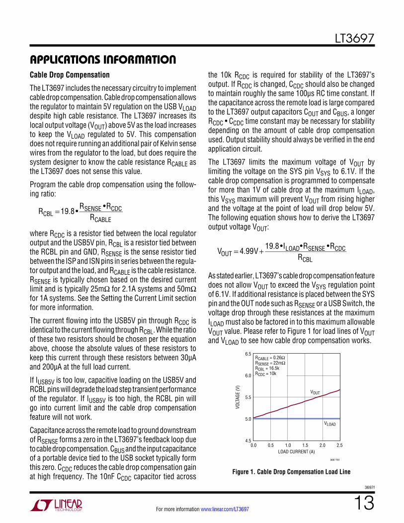
Cable Drop Compensation
The LT3697 includes the necessary circuitry to implement cable drop compensation. Cable drop compensation allows the regulator to maintain 5V regulation on the USB VLOAD despite high cable resistance. The LT3697 increases its local output voltage (VOUT) above 5V as the load increases to keep the VLOAD regulated to 5V. This compensation does not require running an additional pair of Kelvin sense wires from the regulator to the load, but does require the system designer to know the cable resistance RCABLE as the LT3697 does not sense this value.
Program the cable drop compensation using the follow-ing ratio:
RCBL =19.8 •
RSENSE •RCDCRCABLE
where RCDC is a resistor tied between the local regulator output and the USB5V pin, RCBL is a resistor tied between the RCBL pin and GND, RSENSE is the sense resistor tied between the ISP and ISN pins in series between the regula-tor output and the load, and RCABLE is the cable resistance. RSENSE is typically chosen based on the desired current limit and is typically 25mΩ for 2.1A systems and 50mΩ for 1A systems. See the Setting the Current Limit section for more information.
The current flowing into the USB5V pin through RCDC is identical to the current flowing through RCBL. While the ratio of these two resistors should be chosen per the equation above, choose the absolute values of these resistors to keep this current through these resistors between 30µA and 200µA at the full load current.
If IUSB5V is too low, capacitive loading on the USB5V and RCBL pins will degrade the load step transient performance of the regulator. If IUSB5V is too high, the RCBL pin will go into current limit and the cable drop compensation feature will not work.
Capacitance across the remote load to ground downstream of RSENSE forms a zero in the LT3697’s feedback loop due to cable drop compensation. CBUS and the input capacitance of a portable device tied to the USB socket typically form this zero. CCDC reduces the cable drop compensation gain at high frequency. The 10nF CCDC capacitor tied across
applicaTions inForMaTionthe 10k RCDC is required for stability of the LT3697’s output. If RCDC is changed, CCDC should also be changed to maintain roughly the same 100μs RC time constant. If the capacitance across the remote load is large compared to the LT3697 output capacitors COUT and CBUS, a longer RCDC • CCDC time constant may be necessary for stability depending on the amount of cable drop compensation used. Output stability should always be verified in the end application circuit.
The LT3697 limits the maximum voltage of VOUT by limiting the voltage on the SYS pin VSYS to 6.1V. If the cable drop compensation is programmed to compensate for more than 1V of cable drop at the maximum ILOAD, this VSYS maximum will prevent VOUT from rising higher and the voltage at the point of load will drop below 5V. The following equation shows how to derive the LT3697 output voltage VOUT:
VOUT = 4.99V+ 19.8 •ILOAD•RSENSE •RCDCRCBL
As stated earlier, LT3697’s cable drop compensation feature does not allow VOUT to exceed the VSYS regulation point of 6.1V. If additional resistance is placed between the SYS pin and the OUT node such as RSENSE or a USB Switch, the voltage drop through these resistances at the maximum ILOAD must also be factored in to this maximum allowable VOUT value. Please refer to Figure 1 for load lines of VOUT and VLOAD to see how cable drop compensation works.
Figure 1. Cable Drop Compensation Load Line
LOAD CURRENT (A)0.0
4.5
VOLT
AGE
(V)
5.5
6.0
5.0
6.5
2.01.5 2.5
3697 F01
1.00.5
VOUT
VLOAD
RCABLE = 0.26ΩRSENSE = 22mΩRCBL = 16.5kRCDC = 10k
For more information www.linear.com/LT3697
LT3697
143697f
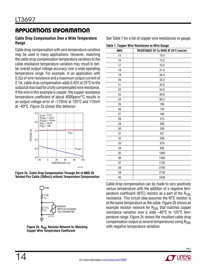
applicaTions inForMaTionCable Drop Compensation Over a Wide Temperature Range
Cable drop compensation with zero temperature variation may be used in many applications. However, matching the cable drop compensation temperature variation to the cable resistance temperature variation may result in bet-ter overall output voltage accuracy over a wide operating temperature range. For example, in an application with 0.2Ω of wire resistance and a maximum output current of 2.1A, cable drop compensation adds 0.42V at 25°C to the output at max load for a fully compensated wire resistance. If the wire in this example is copper, the copper resistance temperature coefficient of about 4000ppm/°C results in an output voltage error of –170mV at 125°C and 110mV at –40°C. Figure 2a shows this behavior.
Figure 2a. Cable Drop Compensation Through 3m of AWG 20 Twisted-Pair Cable (260mΩ) without Temperature Compensation
Figure 2b. RCBL Resistor Network for Matching Copper Wire Temperature Coefficient
17.8k1%
RCBL
3697 F02b
12.1k1%
MURATANCP21XV103J03RA10k THERMISTOR
See Table 1 for a list of copper wire resistances vs gauge.
Table 1. Copper Wire Resistance vs Wire GaugeAWG RESISTANCE OF Cu WIRE AT 20°C (mΩ/m)
15 10.4
16 13.2
17 16.6
18 21.0
19 26.4
20 33.3
21 42.0
22 53.0
23 66.8
24 84.2
25 106
26 134
27 169
28 213
29 268
30 339
31 427
32 538
33 679
34 856
35 1080
36 1360
37 1720
38 2160
39 2730
40 3440
Cable drop compensation can be made to vary positively versus temperature with the addition of a negative tem-perature coefficient (NTC) resistor as a part of the RCBL resistance. This circuit idea assumes the NTC resistor is at the same temperature as the cable. Figure 2b shows an example resistor network for RCBL that matches copper resistance variation over a wide –40°C to 125°C tem-perature range. Figure 2c shows the resultant cable drop compensation output at several temperatures using RCBL with negative temperature variation.
TEMPERATURE (°C)–25
4.8
VOLT
AGE
(V)
5.2
5.4
5.6
5.0
5.8
9565 125
3697 F02a
355
VOUT
VLOAD
ILOAD = 2.1ARCABLE = 0.2ΩRSENSE = 25mΩRCBL = 24.9kRCDC = 10k
For more information www.linear.com/LT3697
LT3697
153697f
applicaTions inForMaTion
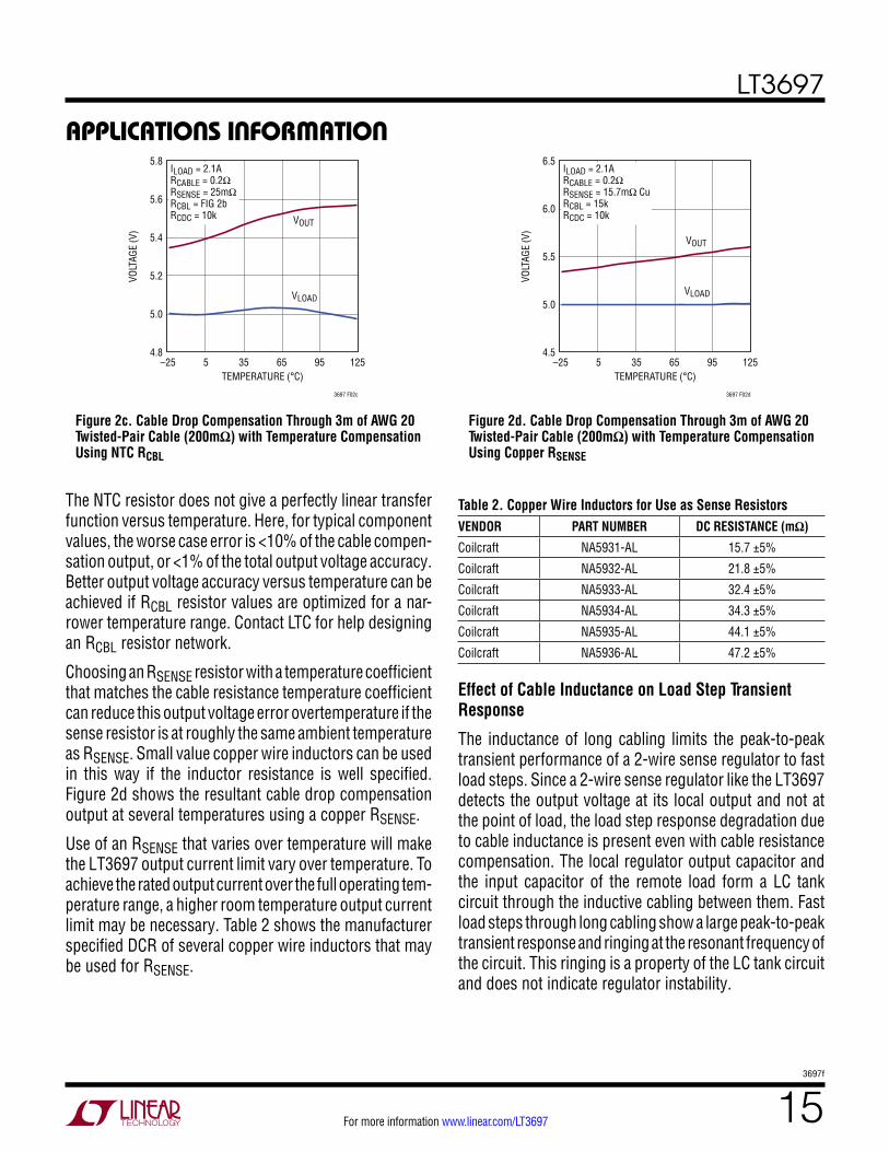
Figure 2c. Cable Drop Compensation Through 3m of AWG 20 Twisted-Pair Cable (200mΩ) with Temperature Compensation Using NTC RCBL
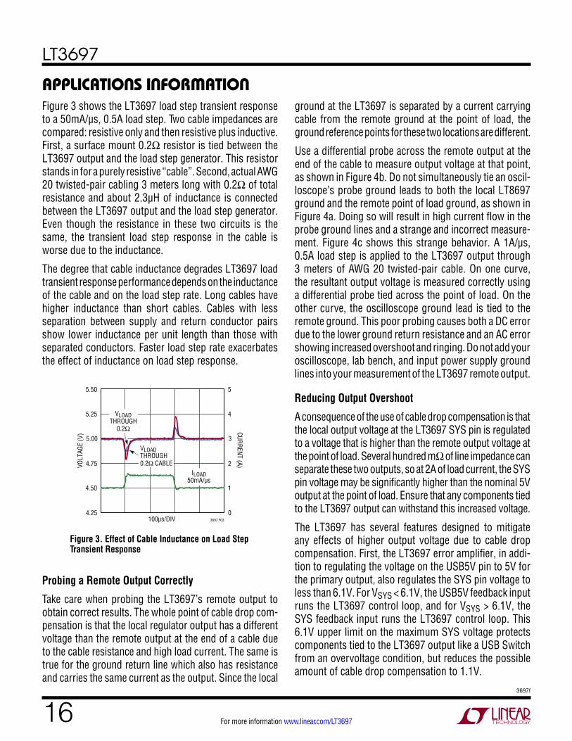
Figure 2d. Cable Drop Compensation Through 3m of AWG 20 Twisted-Pair Cable (200mΩ) with Temperature Compensation Using Copper RSENSE
The NTC resistor does not give a perfectly linear transfer function versus temperature. Here, for typical component values, the worse case error is <10% of the cable compen-sation output, or <1% of the total output voltage accuracy. Better output voltage accuracy versus temperature can be achieved if RCBL resistor values are optimized for a nar-rower temperature range. Contact LTC for help designing an RCBL resistor network.
Choosing an RSENSE resistor with a temperature coefficient that matches the cable resistance temperature coefficient can reduce this output voltage error overtemperature if the sense resistor is at roughly the same ambient temperature as RSENSE. Small value copper wire inductors can be used in this way if the inductor resistance is well specified. Figure 2d shows the resultant cable drop compensation output at several temperatures using a copper RSENSE.
Use of an RSENSE that varies over temperature will make the LT3697 output current limit vary over temperature. To achieve the rated output current over the full operating tem-perature range, a higher room temperature output current limit may be necessary. Table 2 shows the manufacturer specified DCR of several copper wire inductors that may be used for RSENSE.
Table 2. Copper Wire Inductors for Use as Sense ResistorsVENDOR PART NUMBER DC RESISTANCE (mΩ)
Coilcraft NA5931-AL 15.7 ±5%
Coilcraft NA5932-AL 21.8 ±5%
Coilcraft NA5933-AL 32.4 ±5%
Coilcraft NA5934-AL 34.3 ±5%
Coilcraft NA5935-AL 44.1 ±5%
Coilcraft NA5936-AL 47.2 ±5%
Effect of Cable Inductance on Load Step Transient Response
The inductance of long cabling limits the peak-to-peak transient performance of a 2-wire sense regulator to fast load steps. Since a 2-wire sense regulator like the LT3697 detects the output voltage at its local output and not at the point of load, the load step response degradation due to cable inductance is present even with cable resistance compensation. The local regulator output capacitor and the input capacitor of the remote load form a LC tank circuit through the inductive cabling between them. Fast load steps through long cabling show a large peak-to-peak transient response and ringing at the resonant frequency of the circuit. This ringing is a property of the LC tank circuit and does not indicate regulator instability.
TEMPERATURE (°C)–25
4.8
VOLT
AGE
(V)
5.2
5.4
5.6
5.0
5.8
9565 125
3697 F02c
355
VOUT
VLOAD
ILOAD = 2.1ARCABLE = 0.2ΩRSENSE = 25mΩRCBL = FIG 2bRCDC = 10k
TEMPERATURE (°C)–25
4.5
VOLT
AGE
(V)
5.5
6.0
5.0
6.5
9565 125
3697 F02d
355
VOUT
VLOAD
ILOAD = 2.1ARCABLE = 0.2ΩRSENSE = 15.7mΩ CuRCBL = 15kRCDC = 10k
For more information www.linear.com/LT3697
LT3697
163697f
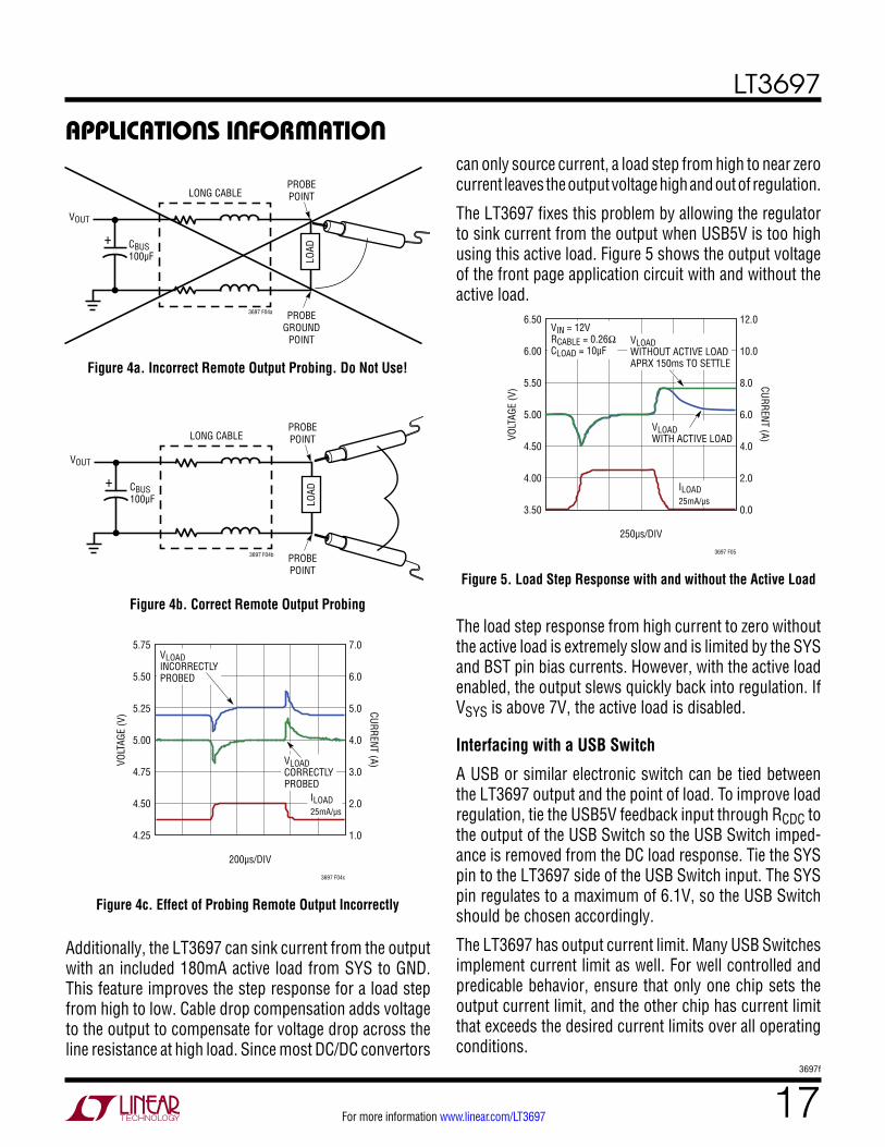
applicaTions inForMaTionFigure 3 shows the LT3697 load step transient response to a 50mA/µs, 0.5A load step. Two cable impedances are compared: resistive only and then resistive plus inductive. First, a surface mount 0.2Ω resistor is tied between the LT3697 output and the load step generator. This resistor stands in for a purely resistive “cable”. Second, actual AWG 20 twisted-pair cabling 3 meters long with 0.2Ω of total resistance and about 2.3µH of inductance is connected between the LT3697 output and the load step generator. Even though the resistance in these two circuits is the same, the transient load step response in the cable is worse due to the inductance.
The degree that cable inductance degrades LT3697 load transient response performance depends on the inductance of the cable and on the load step rate. Long cables have higher inductance than short cables. Cables with less separation between supply and return conductor pairs show lower inductance per unit length than those with separated conductors. Faster load step rate exacerbates the effect of inductance on load step response.
VOLT
AGE
(V) CURRENT (A)
5.00
5.25
5.50
3697 F03
4.75
4.50
4.25
3
4
5
2
1
0100µs/DIV
VLOADTHROUGH
0.2Ω
ILOAD50mA/µs
VLOADTHROUGH0.2Ω CABLE
Figure 3. Effect of Cable Inductance on Load Step Transient Response
Probing a Remote Output Correctly
Take care when probing the LT3697’s remote output to obtain correct results. The whole point of cable drop com-pensation is that the local regulator output has a different voltage than the remote output at the end of a cable due to the cable resistance and high load current. The same is true for the ground return line which also has resistance and carries the same current as the output. Since the local
ground at the LT3697 is separated by a current carrying cable from the remote ground at the point of load, the ground reference points for these two locations are different.
Use a differential probe across the remote output at the end of the cable to measure output voltage at that point, as shown in Figure 4b. Do not simultaneously tie an oscil-loscope’s probe ground leads to both the local LT8697 ground and the remote point of load ground, as shown in Figure 4a. Doing so will result in high current flow in the probe ground lines and a strange and incorrect measure-ment. Figure 4c shows this strange behavior. A 1A/µs, 0.5A load step is applied to the LT3697 output through 3 meters of AWG 20 twisted-pair cable. On one curve, the resultant output voltage is measured correctly using a differential probe tied across the point of load. On the other curve, the oscilloscope ground lead is tied to the remote ground. This poor probing causes both a DC error due to the lower ground return resistance and an AC error showing increased overshoot and ringing. Do not add your oscilloscope, lab bench, and input power supply ground lines into your measurement of the LT3697 remote output.
Reducing Output Overshoot
A consequence of the use of cable drop compensation is that the local output voltage at the LT3697 SYS pin is regulated to a voltage that is higher than the remote output voltage at the point of load. Several hundred mΩ of line impedance can separate these two outputs, so at 2A of load current, the SYS pin voltage may be significantly higher than the nominal 5V output at the point of load. Ensure that any components tied to the LT3697 output can withstand this increased voltage.
The LT3697 has several features designed to mitigate any effects of higher output voltage due to cable drop compensation. First, the LT3697 error amplifier, in addi-tion to regulating the voltage on the USB5V pin to 5V for the primary output, also regulates the SYS pin voltage to less than 6.1V. For VSYS < 6.1V, the USB5V feedback input runs the LT3697 control loop, and for VSYS > 6.1V, the SYS feedback input runs the LT3697 control loop. This 6.1V upper limit on the maximum SYS voltage protects components tied to the LT3697 output like a USB Switch from an overvoltage condition, but reduces the possible amount of cable drop compensation to 1.1V.
For more information www.linear.com/LT3697
LT3697
173697f
applicaTions inForMaTion
Additionally, the LT3697 can sink current from the output with an included 180mA active load from SYS to GND. This feature improves the step response for a load step from high to low. Cable drop compensation adds voltage to the output to compensate for voltage drop across the line resistance at high load. Since most DC/DC convertors
Figure 4a. Incorrect Remote Output Probing. Do Not Use!
Figure 4b. Correct Remote Output Probing
Figure 4c. Effect of Probing Remote Output Incorrectly
+
LOAD
VOUT
CBUS100µF
LONG CABLE
3697 F04a
PROBEPOINT
PROBEGROUND
POINT
+
LOAD
VOUT
CBUS100µF
LONG CABLE
3697 F04b
PROBEPOINT
PROBEPOINT
can only source current, a load step from high to near zero current leaves the output voltage high and out of regulation.
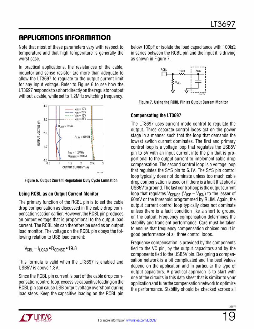
The LT3697 fixes this problem by allowing the regulator to sink current from the output when USB5V is too high using this active load. Figure 5 shows the output voltage of the front page application circuit with and without the active load.
Figure 5. Load Step Response with and without the Active Load
The load step response from high current to zero without the active load is extremely slow and is limited by the SYS and BST pin bias currents. However, with the active load enabled, the output slews quickly back into regulation. If VSYS is above 7V, the active load is disabled.
Interfacing with a USB Switch
A USB or similar electronic switch can be tied between the LT3697 output and the point of load. To improve load regulation, tie the USB5V feedback input through RCDC to the output of the USB Switch so the USB Switch imped-ance is removed from the DC load response. Tie the SYS pin to the LT3697 side of the USB Switch input. The SYS pin regulates to a maximum of 6.1V, so the USB Switch should be chosen accordingly.
The LT3697 has output current limit. Many USB Switches implement current limit as well. For well controlled and predicable behavior, ensure that only one chip sets the output current limit, and the other chip has current limit that exceeds the desired current limits over all operating conditions.
200µs/DIV
VLOADINCORRECTLYPROBED
VLOADCORRECTLYPROBED
ILOAD25mA/µs
4.25
VOLT
AGE
(V) CURRENT (A)
5.75
5.50
5.25
5.00
4.75
4.50
1.0
7.0
6.0
5.0
4.0
3.0
2.0
3697 F04c
250µs/DIV
VLOADWITH ACTIVE LOAD
VIN = 12VRCABLE = 0.26ΩCLOAD = 10µF
ILOAD25mA/µs
3.50VO
LTAG
E (V
) CURRENT (A)
6.50
6.00
5.50
5.00
4.50
4.00
0.0
12.0
10.0
8.0
6.0
4.0
2.0
3697 F05
VLOADWITHOUT ACTIVE LOADAPRX 150ms TO SETTLE

For more information www.linear.com/LT3697
LT3697
183697f
applicaTions inForMaTionThe LT3697 has many of the features of USB Switches such as programmable output current limit, filtered overcurrent fault reporting and on/off functionality. In addition, unlike many USB switches, the LT3697 output survives shorts to 20V, enhancing system robustness. In many cases, a USB Switch therefore is not necessary and the LT3697 can provide both the functionality of a voltage regulator and a USB Switch.
Using SYS as a Secondary Output
For some applications, the SYS pin can be used as a sec-ondary voltage output in addition to the primary voltage output regulated by the USB5V pin. The SYS pin voltage varies between 5V and 6.1V depending on the load cur-rent if cable drop compensation is used on the primary output. A 3.3V low dropout regulator can be tied to SYS to provide a secondary regulated output such as to power a USB µController. This SYS output will have neither cable drop compensation nor output current limit, so the load on the SYS pin should be designed to limit load current. Also, an electronic switch may be necessary to prevent an output overcurrent condition on the USB5V output from bringing down the SYS output. See the inductor selection and maximum output current discussion below to deter-mine how much total load current can be drawn from the SYS and USB5V outputs for a given LT3697 application.
Setting the Current Limit
In addition to regulating the output voltage, the LT3697 includes a current regulation loop for setting the average output current limit as shown in the Typical Applications section.
The LT3697 measures the voltage drop across an external current sense resistor using the ISP and ISN pins. This resistor should be connected in series with the load cur-rent after the output capacitor. The LT3697 control loop modulates the cycle-by-cycle switch current limit such that the average voltage across the ISP–ISN pins does not exceed its regulation point.
The LT3697 output current limit can be programmed by tying a resistor from RLIM to ground. Program the current limit using the following equation:
RLIM = (ILIM • RSENSE • 1.848) – 8.49
Where ILIM is the output current limit in amps, RSENSE is the resistance in mΩ tied between the ISP and ISN pins, and RLIM is the resistance in kΩ tied from the RLIM pin to ground.
The preceding ILIM equation is valid for VISP – VISN < 60mV. At 60mV VSENSE, the internal current limit loop takes over output current regulation from the RLIM pin. The maximum programmable output current is therefore found by the following equation:
ILIMMAX=
60mVRSENSE
The internal 11µA pull-up on the RLIM pin allows this pin to be floated if unused, in which case the ILIMMAX would be the output current limit.
The LT3697’s output current limit loop cannot regulate to zero output current even if the RLIM pin is grounded. RLIM can program the output current down to 1/3 of the maximum value, or VSENSE = 20mV.
The LT3697’s ability to regulate the output current is limited by its tON(MIN). In this scenario, at very low output voltage the output current can exceed the programmed output current limit and is limited by the output overcurrent threshold of VSENSE = 70mV. To help mitigate this effect, at low output voltage the LT3697 folds back the switching frequency to 240kHz (at VSYS = 0V) to allow regulation at very low duty cycle. Also, above VIN = 35V the LT3697 stops switching. For VIN < 35V, use the following equation to find the minimum output voltage (VOUT(MIN)) where the LT8697 can regulate the output current limit:
VOUT(MIN) = 240kHz • tON(MIN) • (VIN – VSW + VD) – VD – VSENSE – VL
where tON(MIN) is the minimum on-time (110ns at 25°C), VSW is the internal switch drop of 1.6V without BST at 2A, VD is the Schottky catch diode forward drop, VSENSE is voltage across the RSENSE at the programmed output current and VL is the resistive drop across the inductor ESR at the programmed output current. If the calculated VOUT(MIN) is negative or is less than the IR drop across the resistive short on the output at the programmed current limit, then the LT3697 regulates the output current limit.
For more information www.linear.com/LT3697
LT3697
193697f
Figure 7. Using the RCBL Pin as Output Current Monitor
Note that most of these parameters vary with respect to temperature and that high temperature is generally the worst case.
In practical applications, the resistances of the cable, inductor and sense resistor are more than adequate to allow the LT3697 to regulate to the output current limit for any input voltage. Refer to Figure 6 to see how the LT3697 responds to a short directly on the regulator output without a cable, while set to 1.2MHz switching frequency.
applicaTions inForMaTionbelow 100pF or isolate the load capacitance with 100kΩ in series between the RCBL pin and the input it is driving as shown in Figure 7.
Figure 6. Output Current Regulation Duty Cycle Limitation
Using RCBL as an Output Current Monitor
The primary function of the RCBL pin is to set the cable drop compensation as discussed in the cable drop com-pensation section earlier. However, the RCBL pin produces an output voltage that is proportional to the output load current. The RCBL pin can therefore be used as an output load monitor. The voltage on the RCBL pin obeys the fol-lowing relation to USB load current:
VCBL = ILOAD •RSENSE •19.8
This formula is valid when the LT3697 is enabled and USB5V is above 1.3V.
Since the RCBL pin current is part of the cable drop com-pensation control loop, excessive capacitive loading on the RCBL pin can cause USB output voltage overshoot during load steps. Keep the capacitive loading on the RCBL pin
100k ADC
3697 F07
RCBL
RCBL
Compensating the LT3697
The LT3697 uses current mode control to regulate the output. Three separate control loops act on the power stage in a manner such that the loop that demands the lowest switch current dominates. The first and primary control loop is a voltage loop that regulates the USB5V pin to 5V with an input current into the pin that is pro-portional to the output current to implement cable drop compensation. The second control loop is a voltage loop that regulates the SYS pin to 6.1V. The SYS pin control loop typically does not dominate unless too much cable drop compensation is used or if there is a fault that shorts USB5V to ground. The last control loop is the output current loop that regulates VSENSE (VISP – VISN) to the lesser of 60mV or the threshold programmed by RLIM. Again, the output current control loop typically does not dominate unless there is a fault condition like a short to ground on the output. Frequency compensation determines the stability and transient performance. Care must be taken to ensure that frequency compensation choices result in good performance of all three control loops.
Frequency compensation is provided by the components tied to the VC pin, by the output capacitors and by the components tied to the USB5V pin. Designing a compen-sation network is a bit complicated and the best values depend on the application and in particular the type of output capacitors. A practical approach is to start with one of the circuits in this data sheet that is similar to your application and tune the compensation network to optimize the performance. Stability should be checked across all
OUTPUT CURRENT (A)
0.0
OUTP
UT V
OLTA
GE (V
)
4.0
3.0
2.0
1.0
32.521.510.5
3697 F06
VIN = 28VVIN = 12VVIN = 28VVIN = 12V
RLIM = 29.4k
fSW = 1.2MHzRSENSE = 25mΩ
RLIM = OPEN
For more information www.linear.com/LT3697
LT3697
203697f
applicaTions inForMaTionoperating conditions, including load current, input voltage, and temperature. The LT1375 data sheet contains a more thorough discussion of loop compensations and describes how to test stability using a transient load. Contact Linear Technology Corp for help compensating the LT3697 if your application circuit is significantly different than those shown in this data sheet.
Setting the Switching Frequency
The LT3697 uses a constant frequency PWM architecture that can be programmed to switch from 300kHz to 2.2MHz by using a resistor tied from the RT pin to ground. A table showing the necessary RT value for a desired switching frequency is in Table 3.
Table 3. Switching Frequency vs RT ValueSwitching Frequency (MHz) RT (kΩ)
2.200 18.7
2.100 20.5
2.000 22.1
1.900 24.3
1.800 26.1
1.700 28.7
1.600 31.6
1.500 34.8
1.400 39.2
1.300 43.2
1.200 48.7
1.100 54.9
1.000 63.4
0.900 73.2
0.800 86.6
0.700 105
0.600 133
0.500 178
0.400 255
0.300 453
RT can also be found for desired switching frequency using the following formula where f is in MHz:
RT =63.4k
f−0.164−12.4k
Operating Frequency Trade-Offs
Selection of the operating frequency is a trade-off between efficiency, component size, minimum dropout voltage, and maximum input voltage. The advantage of high frequency operation is that smaller inductor and capacitor values may be used. The disadvantages are lower efficiency, and lower maximum input voltage. The highest acceptable switching frequency (fSW(MAX)) for a given application can be calculated as follows:
f SW(MAX)=
VSYS +VDtON(MIN) •(VIN – VSW +VD)
where VIN is the typical input voltage, VD is the catch diode drop (~0.5V), and VSW is the internal switch drop (~0.4V at max load). VSYS can vary between 5V and 6.1V depending on if cable drop compensation is used and how USB5V is tied to SYS. This equation shows that slower switching frequency is necessary to safely accommodate high VIN. This is due to the limitation on the LT3697’s minimum on-time. The minimum on-time is a strong function of temperature. Use the typical minimum on-time curve to design for an application’s maximum temperature, while adding about 30% for part-to-part variation. The minimum duty cycle that can be achieved taking the minimum on time into account is:
DCMIN=fSW • tON(MIN)
where fSW is the switching frequency and tON(MIN) is the minimum switch on-time. A good choice of switching frequency should allow adequate input voltage range (see next two sections) and keep the inductor and capacitor values small.
Maximum Input Voltage Range
The LT3697 can operate from input voltages of up to 35V and withstand voltages up to 60V. Note that while VIN is above ~37V the part will keep the switch off and the output will not be in regulation. Often the highest allowed VIN during normal operation (VIN(OP-MAX)) is limited by the
For more information www.linear.com/LT3697
LT3697
213697f
applicaTions inForMaTionminimum duty cycle rather than the absolute maximum ratings of the VIN pin. It can be calculated using the fol-lowing equation:
VIN(OP−MAX) =
VSYS +VDfSW • tON(MIN)
– VD +VSW
where VD is the catch diode drop and VSW is the internal switch drop. VSYS can vary between 5V and 6.1V depending on if cable drop compensation is used and how USB5V is tied to SYS. A lower switching frequency can be used to extend normal operation to higher input voltages.
The circuit will tolerate inputs above the maximum op-erating input voltage and up to the absolute maximum ratings of the VIN and BOOST pins, regardless of chosen switching frequency. However, during such transients where VIN is higher than VIN(OP-MAX), the LT3697 will enter pulse-skipping operation where some switching pulses are skipped to maintain output regulation. The output voltage ripple and inductor current ripple will be higher than in typical operation. Do not overload the output when VIN is greater than VIN(OP-MAX), unless the ISP and ISN pins are connected such as to limit the output current.
Minimum Input Voltage Range
The minimum input voltage for full frequency operation is determined by either the LT3697’s maximum duty cycle or the enforced minimum dropout voltage. See the Typi-cal Performance Characteristics section for the minimum input voltage across load.
The LT3697 will continue to switch and pull the output as high as possible down to its minimum operating voltage of 4.5V. The duty cycle is the fraction of time that the internal switch is on during a clock cycle. Unlike many fixed frequency regulators, the LT3697 can extend its duty cycle by remaining on for multiple clock cycles. The LT3697 will not switch off at the end of each clock cycle if there is sufficient voltage across the boost capacitor (CBST in the Block Diagram). Eventually, the voltage on the boost capacitor falls and requires refreshing. When this occurs, the switch will turn off, allowing the inductor current to recharge the boost capacitor.
At low VIN, the LT3697 regulates the SYS voltage such that it stays 600mV below VIN. This enforced minimum dropout voltage is due to reasons that are covered in the next section. This places a limitation on the minimum input voltage as follows:
VIN(MIN) = VSYS + VDROPOUT(MIN)
where VDROPOUT(MIN) is the minimum dropout voltage of 600mV. VSYS can vary between 5V and 6.1V depending on if cable drop compensation is used and how USB5V is tied to SYS.
Minimum Dropout Voltage
To achieve a low dropout voltage, the internal power switch must always be able to fully saturate. This means that the boost capacitor, which provides a base drive higher than VIN, must always be able to charge up when the part starts up and then must also stay charged during all operating conditions.
During start-up, if there is insufficient inductor current such as during light load situations, the boost capacitor will be unable to charge. When the LT3697 detects that the boost capacitor is not charged, it activates a 200mA (typical) load on the SYS pin. If the SYS pin is connected to the output, the extra load will increase the inductor current enough to sufficiently charge the boost capacitor. When the boost capacitor is charged, the current source turns off, and the part may re-enter Burst Mode operation.
To keep the boost capacitor charged regardless of load during dropout conditions, a minimum dropout voltage is enforced. When the SYS pin is tied to the output, the LT3697 regulates the output such that:
VIN – VSYS>VDROPOUT(MIN) where VDROPOUT(MIN) is 600mV. The 600mV dropout volt-age limits the duty cycle and forces the switch to turn off regularly to charge the boost capacitor. Since sufficient voltage across the boost capacitor is maintained, the switch is allowed to fully saturate and the internal switch drop stays low for good dropout performance. Figure 8 shows the overall VIN to VOUT performances during start-up and dropout conditions.
For more information www.linear.com/LT3697
LT3697
223697f
applicaTions inForMaTion
Inductor Selection and Maximum Output Current
For a given input and output voltage, the inductor value and switching frequency will determine the ripple current. The ripple current increases with higher VIN or VOUT and decreases with higher inductance and faster switching frequency. A good first choice for the inductor value is:
L = VSYS +VD
1.5 • fSW
where fSW is the switching frequency in MHz, VSYS is the SYS pin voltage, VD is the catch diode drop (~0.5V) and L is the inductor value is μH.
The inductor’s RMS current rating must be greater than the maximum load current and its saturation current should be about 30% higher. For robust operation in fault conditions (start-up or short circuit) and high input voltage (>30V), the saturation current should be above 7A. To keep the efficiency high, the series resistance (DCR) should be less than 0.1Ω, and the core material should be intended for high frequency applications. Table 4 lists several inductor vendors.
Table 4. Inductor VendorsVENDOR URL
Coilcraft www.coilcraft.com
Sumida www.sumida.com
Toko www.tokoam.com
Würth Electronik www.we-online.com
Coiltronics www.cooperet.com
Murata www.murata.com
The inductor value must be sufficient to supply the desired maximum output current (IOUT(MAX)), which is a function of the switch current limit (ILIM) and the ripple current.
IOUT(MAX) = ILIM –
ΔIL2
The LT3697 limits its peak switch current in order to protect itself and the system from overload faults. The LT3697’s switch current limit (ILIM) is 5.3A at low duty cycles and decreases linearly to 4A at DC = 0.8.
When the switch is off, the potential across the inductor is the output voltage plus the catch diode drop. This gives the peak-to-peak ripple current in the inductor:
ΔIL=
(1–DC)•(VSYS +VD)L • fSW
where fSW is the switching frequency of the LT3697, DC is the duty cycle and L is the value of the inductor. Therefore, the maximum output current that the LT3697 will deliver depends on the switch current limit, the inductor value, and the input and output voltages. The inductor value may have to be increased if the inductor ripple current does not allow sufficient maximum output current (IOUT(MAX)) given the switching frequency and maximum input voltage used in the desired application.
The optimum inductor for a given application may differ from the one indicated by this simple design guide. A larger value inductor provides a higher maximum load current and reduces the output voltage ripple. If your load is lower than the maximum load current, than you can relax the value of the inductor and operate with higher ripple cur-rent. This allows you to use a physically smaller inductor, or one with a lower DCR resulting in higher efficiency. Be aware that if the inductance differs from the simple rule above, then the maximum load current will depend on the input voltage. In addition, low inductance may result in discontinuous mode operation, which further reduces maximum load current. For discussion regarding maximum output current and discontinuous operation, see Linear Technology’s Application Note 44. Additionally, for duty cycles greater than 50% (VOUT/VIN > 0.5), a minimum inductance is required to avoid subharmonic oscillations, see Application Note 19.
Figure 8. VIN to VOUT Performance
RLOAD = 100Ω(50mA IN REGULATION)RCBL = ∞
100ms/DIV
2V/DIV
3697 F08
VIN
VOUT
For more information www.linear.com/LT3697
LT3697
233697f
applicaTions inForMaTionOne approach to choosing the inductor is to start with the simple rule given above, look at the available inductors, and choose one to meet cost or space goals. Then use the equations above to check that the LT3697 will be able to deliver the required output current. Note again that these equations assume that the inductor current is continuous. Discontinuous operation occurs when IOUT is less than:
ΔIL2
Input Capacitor
Bypass the input of the LT3697 circuit with a ceramic capaci-tor of X7R or X5R type. Y5V types have poor performance over temperature and applied voltage, and should not be used. A 4.7μF to 10μF ceramic capacitor is adequate to bypass the LT3697 and will easily handle the ripple cur-rent. Note that larger input capacitance is required when a lower switching frequency is used (due to longer on times). If the input power source has high impedance, or there is significant inductance due to long wires or cables, additional bulk capacitance may be necessary. This can be provided with a low performance electrolytic capacitor.
Step-down regulators draw current from the input sup-ply in pulses with very fast rise and fall times. The input capacitor is required to reduce the resulting voltage ripple at the LT3697 input and to force this very high frequency switching current into a tight local loop, minimizing EMI. A 4.7μF capacitor is capable of this task, but only if it is placed close to the LT3697 (see the PCB Layout section). A second precaution regarding the ceramic input capacitor concerns the maximum input voltage rating of the LT3697. A ceramic input capacitor combined with trace or cable inductance forms a high quality (under damped) tank circuit. If the LT3697 circuit is plugged into a live supply, the input voltage can ring to twice its nominal value, pos-sibly exceeding the LT3697’s voltage rating. If the input supply is poorly controlled or the user will be plugging the LT3697 into an energized supply, the input network should be designed to prevent this overshoot. See Linear Technology Application Note 88 for a complete discussion.
Output Capacitor and Output Ripple
The LT3697 output capacitors include COUT tied to the inductor and to the ISP side of RSENSE and CBUS tied to the regulator output and the ISN side of RSENSE. These output capacitors have two essential functions. Along with the inductor, they filter the square wave generated by the LT3697 to produce the DC output. In particular, COUT determines the output ripple, so low impedance (at the switching frequency) is important. The second function is to store energy in order to satisfy transient loads and stabilize the LT3697’s control loop.
CBUS serves some additional purposes. It helps to stabilize the output current limit loop. To this end, CBUS must satisfy the following relationship:
CBUS ≥ COUT
CBUS also helps provide the minimum 120µF bypassing required for the VBUS rail as specified by the USB 2.0 standard document.
Ceramic capacitors have very low equivalent series re-sistance (ESR) and provide the best ripple performance. A good starting value for COUT is 47µF in 1206 or 1210 case size. Use X5R or X7R types. A good starting value for CBUS is 100µF. Since CBUS is only tied to the inductor through RSENSE, the ESR rating of CBUS is less critical and high density tantalum or electrolytic capacitor types may be used.
When choosing a capacitor, look carefully through the data sheet to find out what the actual capacitance is under operating conditions (applied voltage and temperature). A physically larger capacitor or one with a higher voltage rating may be required. Table 5 lists several capacitor vendors.
Table 5. Recommended Ceramic Capacitor VendorsMANUFACTURER URL
AVX www.avxcorp.com
Murata www.murata.com
Taiyo Yuden www.t-yuden.com
Vishay Siliconix www.vishay.com
TDK www.tdk.com
For more information www.linear.com/LT3697
LT3697
243697f
applicaTions inForMaTionCatch Diode Selection
The catch diode (DCATCH from the Block Diagram) conducts current only during the switch off time. Average forward current in normal operation can be calculated from:
ID(AVG)= IOUT •
VIN – VSYS( )VIN
where IOUT is the output load current. The current rating of the diode should be selected to be greater than or equal to the application’s output load current, so that the diode is robust for a wide input voltage range. The voltage rating of the diode is equal to the maximum regulator input voltage while switching, 37V or less. Use a 3A, 40V Schottky diode. Do not use a 60V diode due to the high resistive voltage drop.
BST and SYS Pin Considerations
Capacitor CBST and Schottky diode DBST (see the Block Diagram) are used to generate a boost voltage that is higher than the input voltage to drive the internal NPN power switch. In most cases a 0.47μF capacitor will work well for CBST. For switching frequency below 500kHz, use 1µF. The BST pin must be more than 1.8V above the SW pin for best efficiency and more than 2.6V above the SW pin to allow the LT3697 to skip off times to achieve very high duty cycles.
With the SYS pin connected to the output, a 180mA ac-tive load will charge the boost capacitor during light load start-up and an enforced 600mV minimum dropout voltage will keep the boost capacitor charged across operating conditions (see Minimum Dropout Voltage section).
Enable
The LT3697 is in shutdown with IVIN < 1µA when the EN pin is low and active when the pin is high. The enable threshold is about 1.5V. The EN pin can be tied to VIN if the shutdown feature is not used. The EN pin current depends on the EN pin voltage for VEN < 12V and reaches about 30µA at 12V.
Synchronization
To select low ripple Burst Mode operation, tie the SYNC pin below 0.3V (this can be ground or a logic output).
Synchronizing the LT3697 oscillator to an external fre-quency can be done by connecting a square wave (with on and off time greater than 50ns) to the SYNC pin. The square wave amplitude should have valleys that are below 0.4V and peaks above 1V (up to 6V).
The LT3697 will skip pulses at low output loads while synchronized to an external clock to maintain regula-tion. At very light loads, the part will go to sleep between groups of pulses, reducing the quiescent current of the part. Holding the SYNC pin DC high yields no advantages so it is not recommended.
The LT3697 may be synchronized over a 300kHz to 2.2MHz range. The RT resistor should be chosen to set the LT3697 switching frequency 10% below the lowest synchronization input. For example, if the synchroniza-tion signal will be 300kHz and higher, the RT should be selected for 270kHz. To ensure reliable and safe operation the LT3697 will only synchronize when the output voltage is near regulation. It is therefore necessary to choose a large enough inductor value to supply the required output current at the frequency set by the RT resistor (see Induc-tor Selection section). The slope compensation is set by the RT value, while the minimum slope compensation required to avoid subharmonic oscillations is established by the inductor size, input voltage and output voltage. Since the synchronization frequency will not change the slopes of the inductor current waveform, if the inductor is large enough to avoid subharmonic oscillations at the frequency set by RT, than the slope compensation will be sufficient for all synchronization frequencies.
Shorted and Reversed Input Protection
If the inductor is chosen so that it won’t saturate excessively, the LT3697 will tolerate a shorted output and the power dissipation will be limited by the current limit set by RLIM and RSENSE (see the Setting the Current Limit section).
There is another situation to consider in systems where the output will be held high when the input to the LT3697 is absent. This may occur in automotive systems where the LT3697 output may be connected to the 12V VBATT during a fault condition or if a USB peripheral with a large, charged cap is plugged into the LT3697 output. If the VIN pin is allowed to float and the EN pin is held high

For more information www.linear.com/LT3697
LT3697
253697f
(either by a logic signal or because it is tied to VIN), then the LT3697’s internal circuitry will pull its quiescent cur-rent through its SW pin. This is fine if your system can tolerate a 1mA in this state. If you ground the EN pin, the SW pin current will drop to zero. However, if the VIN pin is grounded while the output is held high, regardless of EN, parasitic diodes inside the LT3697 can pull current from the output through the SW pin and out of VIN pin, possibly causing high power dissipation in and damage to the LT3697 depending on the magnitude of the current. Figure 9 shows a circuit that is robust to output shorts high and reversed input.
The exposed pad on the bottom of the package must be soldered to ground so that the pad acts as a heat sink. To keep thermal resistance low, extend the ground plane as much as possible, and add thermal vias under and near the LT3697 to additional ground planes within the circuit board and on the bottom side.
High Temperature Considerations and Thermal Shutdown
For higher ambient temperatures, care should be taken in the layout of the PCB to ensure good heat sinking of the LT3697. The exposed pad on the bottom of the package must be soldered to a ground plane. This ground should be tied to large copper layers below with thermal vias; these layers will dissipate the heat generated by the LT3697. Placing additional vias can reduce the thermal resistance further. When operating at high ambient temperatures, the maximum load current should be derated as the ambient temperature approaches the maximum junction rating.
Power dissipation within the LT3697 can be estimated by calculating the total power loss from an efficiency measure-ment and subtracting the catch diode loss and inductor loss. The die temperature is calculated by multiplying the LT3697 power dissipation by the thermal resistance from junction to ambient.
The LT3697 has thermal shutdown to protect the part during periods of high power dissipation, particularly in high ambient temperature environments. The thermal shutdown feature detects when the LT3697 is too hot and shuts the part down, preventing switching. When the thermal event passes and the LT3697 cools, the part will restart and resume switching.
Other Linear Technology Publications
Application Notes 19, 35 and 44 contain more detailed descriptions and design information for buck regulators and other switching regulators. The LT1376 data sheet has a more extensive discussion of output ripple, loop compensation and stability testing.
applicaTions inForMaTion
Figure 9. Diodes DIN and DOUT Prevent High Current Flow in the LT3697 if the Input Is Grounded or Floating and the Output Is Pulled High.
INPUT OUTPUT
3697 F09
LT3697
GND
COUTCIN
VIN SWDIN
DOUT
CBULK
L
+
PCB Layout
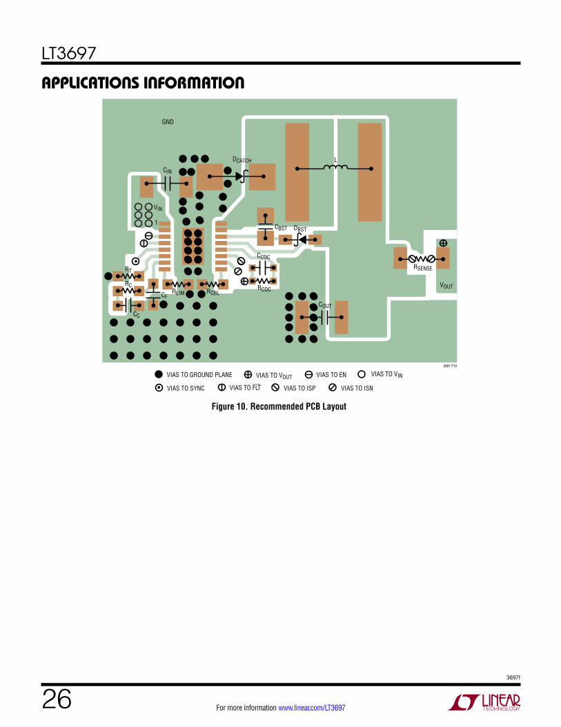
For proper operation and minimum EMI, care must be taken during printed circuit board layout. Figure 10 shows a good PCB layout example with component, trace, ground plane and via locations. Note that large currents with high dI/dt flow in the LT3697’s VIN and SW pins, the catch diode (DCATCH), and the input capacitor (CIN). The loop formed by these components should be as small and low inductance as possible. These components, along with the inductor and output capacitor, should be placed on the same side of the circuit board, and their connections should be made on that layer. Place a local, unbroken ground plane below these components. The SW and BST nodes should be as small as possible to minimize the capacitive coupling on these nodes to any fixed voltage like GND or VIN. Finally, keep the VC, RT, RLIM and RCBL nodes small so that the ground traces will shield them from the SW and BST nodes.
For more information www.linear.com/LT3697
LT3697
263697f
applicaTions inForMaTion
Figure 10. Recommended PCB Layout
CIN
VIN
1
GND
3697 F10
DCATCH L
RT
RLIM RCBLRCDC
CCDC
COUT
VOUT
RSENSE
CBST DBST
RC
CC
CF
VIAS TO GROUND PLANE VIAS TO VOUT VIAS TO EN
VIAS TO FLT VIAS TO ISP VIAS TO ISN
VIAS TO VIN
VIAS TO SYNC
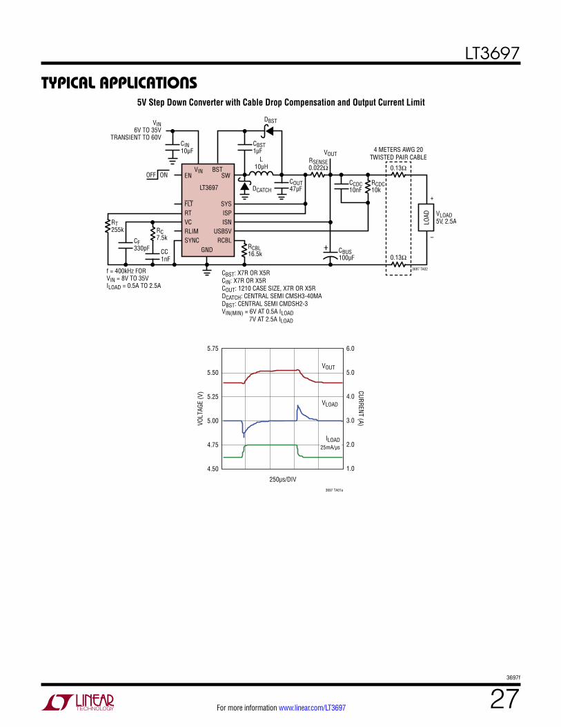
For more information www.linear.com/LT3697
LT3697
273697f
Typical applicaTions5V Step Down Converter with Cable Drop Compensation and Output Current Limit
RSENSE0.022Ω
DBST
DCATCH
0.13ΩL
10µH
CIN10µF
VIN BST
LT3697
EN SW
SYSISPISN
USB5VRCBL
FLTRTVCRLIMSYNC
GNDCF330pF CC
1nF
CBST1µF
COUT47µF
CBUS100µF
RCDC10k
CCDC10nF
VIN6V TO 35V
TRANSIENT TO 60V
0.13Ω
RT255k
f = 400kHz FORVIN = 8V TO 35VILOAD = 0.5A TO 2.5A
RC7.5k
RCBL16.5k
3697 TA02
4 METERS AWG 20TWISTED PAIR CABLE
VOUT
VLOAD5V, 2.5ALO
AD
–
+
ONOFF
+
CBST: X7R OR X5RCIN: X7R OR X5RCOUT: 1210 CASE SIZE, X7R OR X5RDCATCH: CENTRAL SEMI CMSH3-40MADBST: CENTRAL SEMI CMDSH2-3VIN(MIN) = 6V AT 0.5A ILOAD 7V AT 2.5A ILOAD
250µs/DIV3697 TA01a
5.75
5.50
5.25
5.00
4.75
4.50
VOLT
AGE
(V)
6.0
5.0
4.0
3.0
2.0
1.0
CURRENT (A)
ILOAD25mA/µs
VLOAD
VOUT
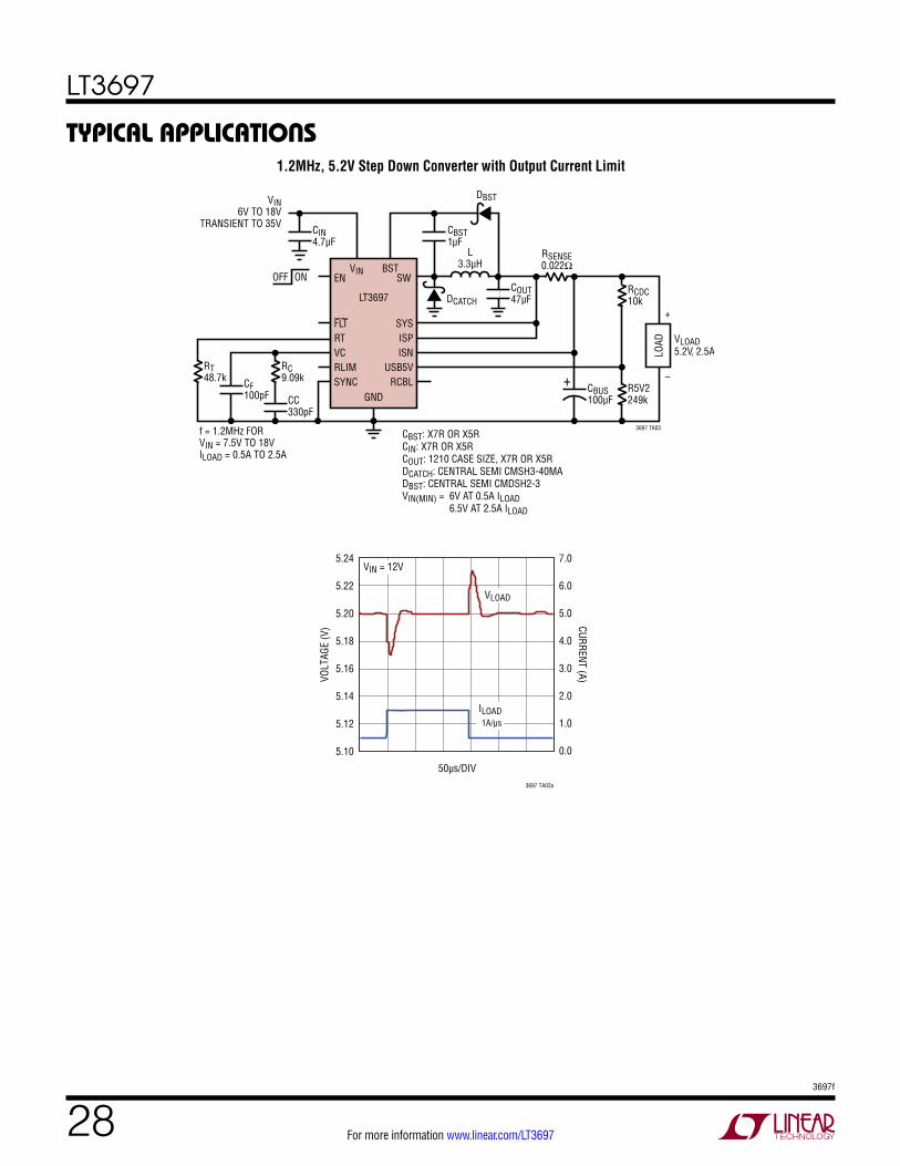
For more information www.linear.com/LT3697
LT3697
283697f
Typical applicaTions1.2MHz, 5.2V Step Down Converter with Output Current Limit
RSENSE0.022Ω
DBST
DCATCH
L3.3µH
CIN4.7µF
VIN BST
LT3697
EN SW
SYSISPISN
USB5VRCBL
FLTRTVCRLIMSYNC
GNDCF100pF CC
330pF
CBST1µF
COUT47µF
CBUS100µF
RCDC10k
VIN6V TO 18V
TRANSIENT TO 35V
R5V2249k
RT48.7k
f = 1.2MHz FORVIN = 7.5V TO 18VILOAD = 0.5A TO 2.5A
RC9.09k
3697 TA03
VLOAD5.2V, 2.5ALO
AD
–
+
ONOFF
+
CBST: X7R OR X5RCIN: X7R OR X5RCOUT: 1210 CASE SIZE, X7R OR X5RDCATCH: CENTRAL SEMI CMSH3-40MADBST: CENTRAL SEMI CMDSH2-3VIN(MIN) = 6V AT 0.5A ILOAD 6.5V AT 2.5A ILOAD
50µs/DIV3697 TA03a
5.24
5.22
5.20
5.18
5.16
5.14
5.12
5.10
VOLT
AGE
(V)
7.0
6.0
5.0
4.0
3.0
2.0
1.0
0.0
CURRENT (A)
ILOAD1A/µs
VLOAD
VIN = 12V
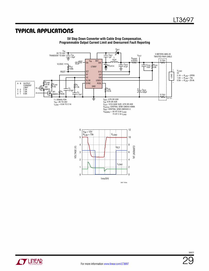
For more information www.linear.com/LT3697
LT3697
293697f
Typical applicaTions5V Step Down Converter with Cable Drop Compensation,
Programmable Output Current Limit and Overcurrent Fault Reporting
RSENSE0.025Ω 0.15Ω
L15µH
CIN10µF
VIN BST
LT3697
EN SW
SYSISPISN
USB5VRCBL
FLTRTVCRLIMSYNC
GNDCF470pF
M1NMOS
M2NMOS
A
COUT47µF
VOUTCBST1µF
RCDC10k
CCDC10nF
VIN6V TO 35V
TRANSIENT TO 60V
VLOGIC
0.15Ω
CBUS100µFRT
453k
f = 300kHz FORVIN = 8V TO 35VILOAD = 0.5A TO 2.1A
RLIM229.4k
RCBL16.5k
3697 TA04
5 METERS AWG 20TWISTED PAIR CABLE
VLOAD5V2.1A - > RLIM = OPEN1.5A - > RLIM = 75k0.5A - > RLIM = 29.4k
LOAD
–
+
ONOFF
DBST
DCATCHRFLT100k
FAULT
RC7.5k
RLIM175k
CC1.5nF
B
A B OUTPUT CURRENT LIMIT0 0 2.4A1 0 1.9A0 1 0.8A
+
CBST: X7R OR X5RCIN: X7R OR X5RCOUT: 1210 CASE SIZE, X7R OR X5RDCATCH: CENTRAL SEMI CMSH3-40MADBST: CENTRAL SEMI CMDSH2-3VIN(MIN) = 6V AT 0.5A ILOAD 7V AT 2.1A ILOAD
1ms/DIV3697 TA04a
6
5
4
3
2
1
0
VOLT
AGE
(V)
12
10
8
6
4
2
0
CURRENT (A)
ILOAD
VLOAD
VFLT
VIN = 12VRLIM = 75k
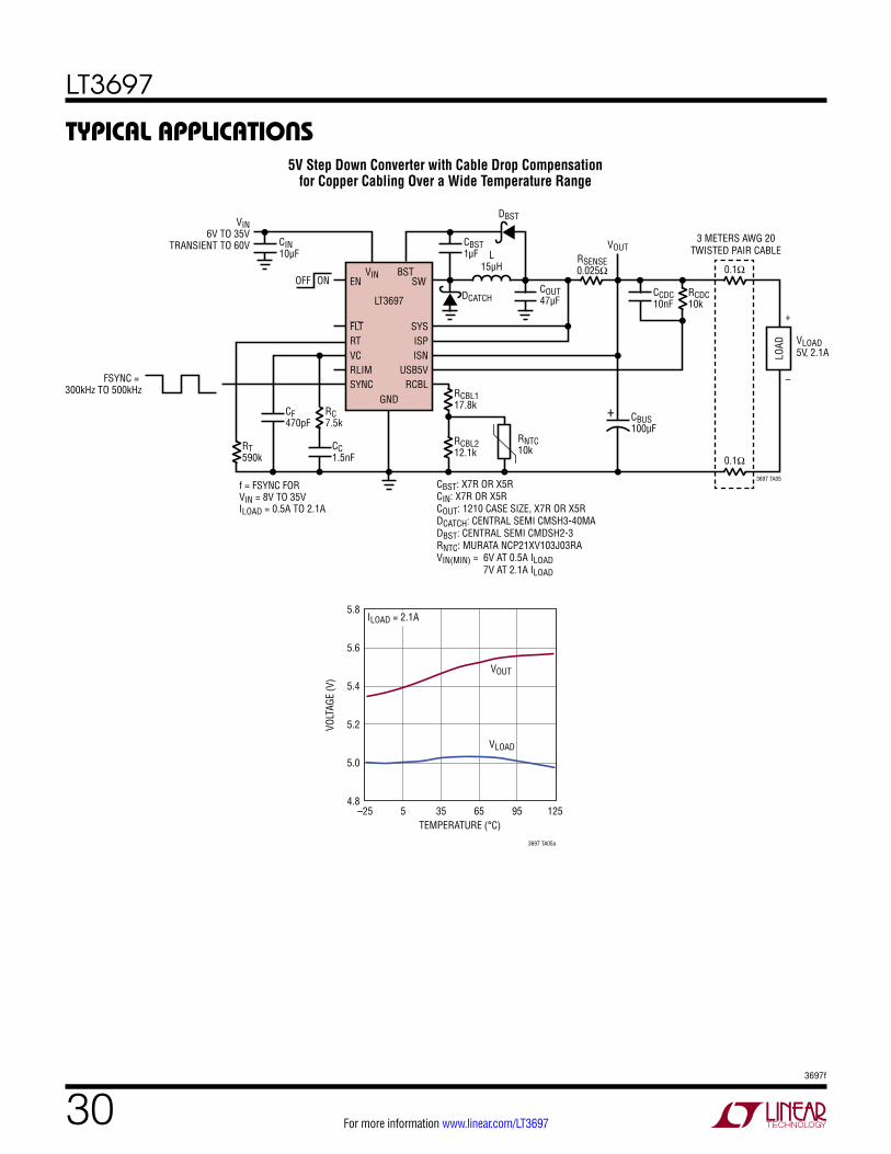
For more information www.linear.com/LT3697
LT3697
303697f
Typical applicaTions5V Step Down Converter with Cable Drop Compensation
for Copper Cabling Over a Wide Temperature Range
RSENSE0.025Ω 0.1Ω
L15µH
CIN10µF
VIN BST
LT3697
EN SW
SYSISPISN
USB5VRCBL
FLTRTVCRLIMSYNC
GNDCF470pF
COUT47µF
VOUTCBST1µF
RCDC10k
CCDC10nF
VIN6V TO 35V
TRANSIENT TO 60V
0.1Ω
CBUS100µF
RT590k
f = FSYNC FORVIN = 8V TO 35VILOAD = 0.5A TO 2.1A
FSYNC = 300kHz TO 500kHz RCBL1
17.8k
3697 TA05
RCBL212.1k
RNTC10k
3 METERS AWG 20TWISTED PAIR CABLE
VLOAD5V, 2.1ALO
AD
–
+
ONOFF
DBST
DCATCH
RC7.5k
CC1.5nF
+
CBST: X7R OR X5RCIN: X7R OR X5RCOUT: 1210 CASE SIZE, X7R OR X5RDCATCH: CENTRAL SEMI CMSH3-40MADBST: CENTRAL SEMI CMDSH2-3RNTC: MURATA NCP21XV103J03RAVIN(MIN) = 6V AT 0.5A ILOAD 7V AT 2.1A ILOAD
TEMPERATURE (°C)–25
4.8
VOLT
AGE
(V)
5.2
5.4
5.6
5.0
5.8
9565 125
3697 TA05a
355
VOUT
VLOAD
ILOAD = 2.1A

For more information www.linear.com/LT3697
LT3697
313697f
Information furnished by Linear Technology Corporation is believed to be accurate and reliable. However, no responsibility is assumed for its use. Linear Technology Corporation makes no representa-tion that the interconnection of its circuits as described herein will not infringe on existing patent rights.
package DescripTionPlease refer to http://www.linear.com/designtools/packaging/ for the most recent package drawings.
MSOP (MSE16) 0213 REV F
0.53 ±0.152(.021 ±.006)
SEATINGPLANE
0.18(.007)
1.10(.043)MAX
0.17 – 0.27(.007 – .011)
TYP
0.86(.034)REF
0.50(.0197)
BSC
16
16151413121110
1 2 3 4 5 6 7 8
9
9
1 8
NOTE:1. DIMENSIONS IN MILLIMETER/(INCH)2. DRAWING NOT TO SCALE3. DIMENSION DOES NOT INCLUDE MOLD FLASH, PROTRUSIONS OR GATE BURRS. MOLD FLASH, PROTRUSIONS OR GATE BURRS SHALL NOT EXCEED 0.152mm (.006") PER SIDE4. DIMENSION DOES NOT INCLUDE INTERLEAD FLASH OR PROTRUSIONS. INTERLEAD FLASH OR PROTRUSIONS SHALL NOT EXCEED 0.152mm (.006") PER SIDE5. LEAD COPLANARITY (BOTTOM OF LEADS AFTER FORMING) SHALL BE 0.102mm (.004") MAX6. EXPOSED PAD DIMENSION DOES INCLUDE MOLD FLASH. MOLD FLASH ON E-PAD SHALL NOT EXCEED 0.254mm (.010") PER SIDE.
0.254(.010) 0° – 6° TYP
DETAIL “A”
DETAIL “A”
GAUGE PLANE
5.10(.201)MIN
3.20 – 3.45(.126 – .136)
0.889 ±0.127(.035 ±.005)
RECOMMENDED SOLDER PAD LAYOUT
0.305 ±0.038(.0120 ±.0015)
TYP
0.50(.0197)
BSC
BOTTOM VIEW OFEXPOSED PAD OPTION
2.845 ±0.102(.112 ±.004)
2.845 ±0.102(.112 ±.004)
4.039 ±0.102(.159 ±.004)
(NOTE 3)
1.651 ±0.102(.065 ±.004)
1.651 ±0.102(.065 ±.004)
0.1016 ±0.0508(.004 ±.002)
3.00 ±0.102(.118 ±.004)
(NOTE 4)
0.280 ±0.076(.011 ±.003)
REF
4.90 ±0.152(.193 ±.006)
DETAIL “B”
DETAIL “B”CORNER TAIL IS PART OF
THE LEADFRAME FEATURE.FOR REFERENCE ONLY
NO MEASUREMENT PURPOSE
0.12 REF
0.35REF
MSE Package16-Lead Plastic MSOP, Exposed Die Pad
(Reference LTC DWG # 05-08-1667 Rev F)
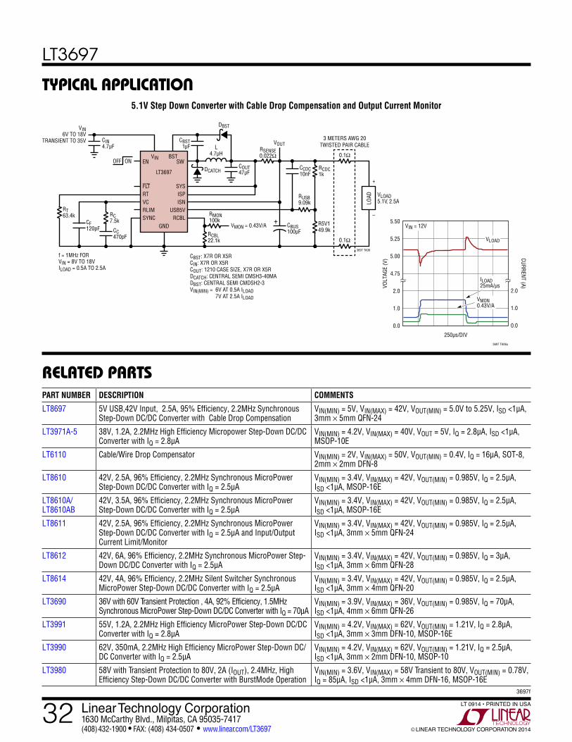
For more information www.linear.com/LT3697
LT3697
323697f
Linear Technology Corporation1630 McCarthy Blvd., Milpitas, CA 95035-7417 (408) 432-1900 FAX: (408) 434-0507 www.linear.com/LT3697 LINEAR TECHNOLOGY CORPORATION 2014
LT 0914 • PRINTED IN USA
relaTeD parTs
Typical applicaTion
PART NUMBER DESCRIPTION COMMENTS
LT8697 5V USB,42V Input, 2.5A, 95% Efficiency, 2.2MHz Synchronous Step-Down DC/DC Converter with Cable Drop Compensation
VIN(MIN) = 5V, VIN(MAX) = 42V, VOUT(MIN) = 5.0V to 5.25V, ISD <1µA, 3mm × 5mm QFN-24
LT3971A-5 38V, 1.2A, 2.2MHz High Efficiency Micropower Step-Down DC/DC Converter with IQ = 2.8µA
VIN(MIN) = 4.2V, VIN(MAX) = 40V, VOUT = 5V, IQ = 2.8µA, ISD <1µA, MSOP-10E
LT6110 Cable/Wire Drop Compensator VIN(MIN) = 2V, VIN(MAX) = 50V, VOUT(MIN) = 0.4V, IQ = 16µA, SOT-8, 2mm × 2mm DFN-8
LT8610 42V, 2.5A, 96% Efficiency, 2.2MHz Synchronous MicroPower Step-Down DC/DC Converter with IQ = 2.5µA
VIN(MIN) = 3.4V, VIN(MAX) = 42V, VOUT(MIN) = 0.985V, IQ = 2.5µA, ISD <1µA, MSOP-16E
LT8610A/LT8610AB
42V, 3.5A, 96% Efficiency, 2.2MHz Synchronous MicroPower Step-Down DC/DC Converter with IQ = 2.5µA
VIN(MIN) = 3.4V, VIN(MAX) = 42V, VOUT(MIN) = 0.985V, IQ = 2.5µA, ISD <1µA, MSOP-16E
LT8611 42V, 2.5A, 96% Efficiency, 2.2MHz Synchronous MicroPower Step-Down DC/DC Converter with IQ = 2.5µA and Input/Output Current Limit/Monitor
VIN(MIN) = 3.4V, VIN(MAX) = 42V, VOUT(MIN) = 0.985V, IQ = 2.5µA, ISD <1µA, 3mm × 5mm QFN-24
LT8612 42V, 6A, 96% Efficiency, 2.2MHz Synchronous MicroPower Step-Down DC/DC Converter with IQ = 2.5µA
VIN(MIN) = 3.4V, VIN(MAX) = 42V, VOUT(MIN) = 0.985V, IQ = 3µA, ISD <1µA, 3mm × 6mm QFN-28
LT8614 42V, 4A, 96% Efficiency, 2.2MHz Silent Switcher Synchronous MicroPower Step-Down DC/DC Converter with IQ = 2.5µA
VIN(MIN) = 3.4V, VIN(MAX) = 42V, VOUT(MIN) = 0.985V, IQ = 2.5µA, ISD <1µA, 3mm × 4mm QFN-20
LT3690 36V with 60V Transient Protection , 4A, 92% Efficiency, 1.5MHz Synchronous MicroPower Step-Down DC/DC Converter with IQ = 70µA
VIN(MIN) = 3.9V, VIN(MAX) = 36V, VOUT(MIN) = 0.985V, IQ = 70µA, ISD <1µA, 4mm × 6mm QFN-26
LT3991 55V, 1.2A, 2.2MHz High Efficiency MicroPower Step-Down DC/DC Converter with IQ = 2.8µA
VIN(MIN) = 4.2V, VIN(MAX) = 62V, VOUT(MIN) = 1.21V, IQ = 2.8µA, ISD <1µA, 3mm × 3mm DFN-10, MSOP-16E
LT3990 62V, 350mA, 2.2MHz High Efficiency MicroPower Step-Down DC/DC Converter with IQ = 2.5µA
VIN(MIN) = 4.2V, VIN(MAX) = 62V, VOUT(MIN) = 1.21V, IQ = 2.5µA, ISD <1µA, 3mm × 2mm DFN-10, MSOP-10
LT3980 58V with Transient Protection to 80V, 2A (IOUT), 2.4MHz, High Efficiency Step-Down DC/DC Converter with BurstMode Operation
VIN(MIN) = 3.6V, VIN(MAX) = 58V Transient to 80V, VOUT(MIN) = 0.78V, IQ = 85µA, ISD <1µA, 3mm × 4mm DFN-16, MSOP-16E
RSENSE0.022Ω 0.1Ω
L4.7µH
CIN4.7µF
VIN BST
LT3697
EN SW
SYSISPISN
USB5VRCBL
FLTRTVCRLIMSYNC
GNDCF120pF CC
470pF
CBST1µF
COUT47µF
CCDC10nF
VIN6V TO 18V
TRANSIENT TO 35V
0.1Ω
R5V149.9k
RUSB9.09k
RCDC1k
RT63.4k
RCBL22.1k
RMON100k
VMON = 0.43V/A
3697 TA06
RC7.5k
3 METERS AWG 20TWISTED PAIR CABLE
VLOAD5.1V, 2.5ALO
AD
–
+
ONOFF
DBST
VOUT
DCATCH
CBUS100µF
f = 1MHz FORVIN = 8V TO 18VILOAD = 0.5A TO 2.5A
CBST: X7R OR X5RCIN: X7R OR X5RCOUT: 1210 CASE SIZE, X7R OR X5RDCATCH: CENTRAL SEMI CMSH3-40MADBST: CENTRAL SEMI CMDSH2-3VIN(MIN) = 6V AT 0.5A ILOAD 7V AT 2.5A ILOAD
+
5.1V Step Down Converter with Cable Drop Compensation and Output Current Monitor
250µs/DIV3697 TA06a
5.50
5.25
5.00
4.75
2.0
1.0
0.0
VOLT
AGE
(V)
2.0
1.0
0.0
CURRENT (A)
ILOAD25mA/µs
VMON0.43V/A
VLOAD
VIN = 12V