Embed Size (px)
Citation preview

LT6658
1Rev. C
For more information www.analog.comDocument Feedback
TYPICAL APPLICATION
FEATURES DESCRIPTION
Precision Dual Output, High Current, Low Noise, Voltage Reference
The LT®6658 is a family of precision dual output references combining the performance of a precision voltage refer-ence and a linear regulator that we call the Refulator™. Both outputs are ideal for driving the reference inputs of high resolution ADCs and DACs, even with heavy load-ing, while simultaneously powering microcontrollers and other circuitry. Both outputs have the same precision specifications and track each other over temperature and load. Each output can be configured with external resis-tors to give an output voltage up to 6V.
Using Kelvin connections, the LT6658 typically has 0.1ppm/mA load regulation with up to 150mA load cur-rent. A noise reduction pin is available to band-limit and lower the total integrated noise.
Separate supply pins are provided for each output, provid-ing an option to reduce power consumption and isolate the buffer amplifiers. The outputs have excellent supply rejection and are stable with 1µF to 50µF capacitors.
The LT6658 is available in a 16-lead MSOP and DFN with an exposed pad for thermal management. Short circuit and thermal protection help to prevent thermal overstress.
Precision Dual Output 2.5V Reference and Supply
Output Voltage Temperature Drift Both Outputs
APPLICATIONS
n Dual Output Tracking Reference n Each Output Configurable to 6V n Output 1: 150mA Source/20mA Sink n Output 2: 50mA Source/20mA Sink
n Low Drift: n A-Grade: 10ppm/°C Max n B-Grade: 20ppm/°C Max
n High Accuracy: n A-Grade: ±0.05% Max n B-Grade: ±0.1% Max
n Low Noise: 1.5ppmP-P (0.1Hz to 10Hz) n Wide Operating Voltage Range to 36V n Load Regulation: 0.25µV/mA n AC PSRR: 96dB at 10kHz n Kelvin Sense Connection on Outputs n Thermal Shutdown n Separate Supply Pins for Each Output n Available Output Voltage Options: 1.2V, 1.8V, 2.5V, 3V,
3.3V, 5V. All Options are Adjustable n Available in Exposed Pad Package MSE16 and
4mm × 3mm DFN
n Microcontroller or FPGA with ADC/DAC Applications n Data Acquisition Systems n Automotive Control and Monitoring n Precision Low Noise Regulators n Instrumentation and Process Control
All registered trademarks and trademarks are the property of their respective owners.
1µF
1µF1µF
0.1µF
VIN5V TO 36V
VOUT22.5V50mA
VOUT12.5V150mA
6658 TA01a
LT6658-2.5
RLOAD2
VIN1
VIN2
VIN
OD
BYPASS
VOUT2_F
VOUT2_S
VOUT1_F
VOUT1_S
GND RLOAD1
ILOAD1 = 150mA
VOUT1VOUT2
TEMPERATURE (°C)–50 –25 0 25 50 75 100 125 150
2.498
2.499
2.500
2.501
2.502
OUTP
UT V
OLTA
GE (V
)
6658 TA01b

LT6658
2Rev. C
For more information www.analog.com
PIN CONFIGURATION
ABSOLUTE MAXIMUM RATINGS
Supply Voltages VIN, VIN1, VIN2 to GND ............................ –0.3V to 38VInput Voltages
OD to GND ............................................. –0.3V to 38V VOUT1_S, VOUT2_S, NR, BYPASS to GND .. –0.3V to 6V
Output Voltages VOUT1_F, VOUT2_F to GND ......................... –0.3V to 6V
Input Current BYPASS ........................................................... ±10mA
(Note 1)
12345678
GNDGND
BYPASSDNC
NRGND
VOUT2_SVOUT2_F
161514131211109
DNCNCVINVOUT1_SVOUT1_FVIN1VIN2OD
TOP VIEW
MSE PACKAGE16-LEAD PLASTIC MSOP
TJMAX = 150°C, θJC = 10°C/W, θJA = 35°C/WDNC: CONNECTED INTERNALLY
DO NOT CONNECT EXTERNAL CIRCUITRY TO THESE PINSEXPOSED PAD (PIN 17) IS GND, MUST BE SOLDERED TO PCB
17GND
161514131211109
17GND
12345678
DNCNCVINVOUT1_SVOUT1_F
VIN1VIN2
OD
GNDGND
BYPASSDNC
NRGND
VOUT2_S
VOUT2_F
TOP VIEW
DE PACKAGE16-LEAD (4mm × 3mm) PLASTIC DFN
TJMAX = 150°C,θJC = 5°C/W, θJA = 43°C/WDNC: CONNECTED INTERNALLY
DO NOT CONNECT EXTERNAL CIRCUITRY TO THESE PINSEXPOSED PAD (PIN 17) IS GND, MUST BE SOLDERED TO PCB
Output Short-Circuit Duration .......................... IndefiniteSpecified Temperature Range
I-Grade.................................................–40°C to 85°C H-Grade ............................................. –40°C to 125°C
Operating Junction Temperature Range . –55°C to 150°CStorage Temperature Range (Note 2) ..... –65°C to 150°CLead Temperature (Soldering, 10 sec)
(Note 3) ............................................................ 300°C

LT6658
3Rev. C
For more information www.analog.com
ORDER INFORMATION
TUBE TAPE AND REEL PART MARKING* PACKAGE DESCRIPTIONSPECIFIED JUNCTION TEMPERATURE RANGE
LT6658AIMSE-1.2#PBF LT6658AIMSE-1.2#TRPBF 665812 16-Lead Plastic MSOP –40°C to 85°C
LT6658BIMSE-1.2#PBF LT6658BIMSE-1.2#TRPBF 665812 16-Lead Plastic MSOP –40°C to 85°C
LT6658AHMSE-1.2#PBF LT6658AHMSE-1.2#TRPBF 665812 16-Lead Plastic MSOP –40°C to 125°C
LT6658BHMSE-1.2#PBF LT6658BHMSE-1.2#TRPBF 665812 16-Lead Plastic MSOP –40°C to 125°C
LT6658AIMSE-1.8#PBF LT6658AIMSE-1.8#TRPBF 665818 16-Lead Plastic MSOP –40°C to 85°C
LT6658BIMSE-1.8#PBF LT6658BIMSE-1.8#TRPBF 665818 16-Lead Plastic MSOP –40°C to 85°C
LT6658AHMSE-1.8#PBF LT6658AHMSE-1.8#TRPBF 665818 16-Lead Plastic MSOP –40°C to 125°C
LT6658BHMSE-1.8#PBF LT6658BHMSE-1.8#TRPBF 665818 16-Lead Plastic MSOP –40°C to 125°C
LT6658AIMSE-2.5#PBF LT6658AIMSE-2.5#TRPBF 665825 16-Lead Plastic MSOP –40°C to 85°C
LT6658BIMSE-2.5#PBF LT6658BIMSE-2.5#TRPBF 665825 16-Lead Plastic MSOP –40°C to 85°C
LT6658AHMSE-2.5#PBF LT6658AHMSE-2.5#TRPBF 665825 16-Lead Plastic MSOP –40°C to 125°C
LT6658BHMSE-2.5#PBF LT6658BHMSE-2.5#TRPBF 665825 16-Lead Plastic MSOP –40°C to 125°C
LT6658AIMSE-3#PBF LT6658AIMSE-3#TRPBF 66583 16-Lead Plastic MSOP –40°C to 85°C
LT6658BIMSE-3#PBF LT6658BIMSE-3#TRPBF 66583 16-Lead Plastic MSOP –40°C to 85°C
LT6658AHMSE-3#PBF LT6658AHMSE-3#TRPBF 66583 16-Lead Plastic MSOP –40°C to 125°C
LT6658BHMSE-3#PBF LT6658BHMSE-3#TRPBF 66583 16-Lead Plastic MSOP –40°C to 125°C
LT6658AIMSE-3.3#PBF LT6658AIMSE-3.3#TRPBF 665833 16-Lead Plastic MSOP –40°C to 85°C
LT6658BIMSE-3.3#PBF LT6658BIMSE-3.3#TRPBF 665833 16-Lead Plastic MSOP –40°C to 85°C
LT6658AHMSE-3.3#PBF LT6658AHMSE-3.3#TRPBF 665833 16-Lead Plastic MSOP –40°C to 125°C
LT6658BHMSE-3.3#PBF LT6658BHMSE-3.3#TRPBF 665833 16-Lead Plastic MSOP –40°C to 125°C
LT6658AIMSE-5#PBF LT6658AIMSE-5#TRPBF 66585 16-Lead Plastic MSOP –40°C to 85°C
LT6658BIMSE-5#PBF LT6658BIMSE-5#TRPBF 66585 16-Lead Plastic MSOP –40°C to 85°C
LT6658AHMSE-5#PBF LT6658AHMSE-5#TRPBF 66585 16-Lead Plastic MSOP –40°C to 125°C
LT6658BHMSE-5#PBF LT6658BHMSE-5#TRPBF 66585 16-Lead Plastic MSOP –40°C to 125°C
LT6658AIDE-1.2#PBF LT6658AIDE-1.2#TRPBF 65812 16-Lead (4mm × 3mm) Plastic DFN –40°C to 85°C
LT6658BIDE-1.2#PBF LT6658BIDE-1.2#TRPBF 65812 16-Lead (4mm × 3mm) Plastic DFN –40°C to 85°C
LT6658AHDE-1.2#PBF LT6658AHDE-1.2#TRPBF 65812 16-Lead (4mm × 3mm) Plastic DFN –40°C to 125°C
LT6658BHDE-1.2#PBF LT6658BHDE-1.2#TRPBF 65812 16-Lead (4mm × 3mm) Plastic DFN –40°C to 125°C
LT6658AIDE-1.8#PBF LT6658AIDE-1.8#TRPBF 65818 16-Lead (4mm × 3mm) Plastic DFN –40°C to 85°C
LT6658BIDE-1.8#PBF LT6658BIDE-1.8#TRPBF 65818 16-Lead (4mm × 3mm) Plastic DFN –40°C to 85°C
LT6658AHDE-1.8#PBF LT6658AHDE-1.8#TRPBF 65818 16-Lead (4mm × 3mm) Plastic DFN –40°C to 125°C
LT6658BHDE-1.8#PBF LT6658BHDE-1.8#TRPBF 65818 16-Lead (4mm × 3mm) Plastic DFN –40°C to 125°C
LT6658AIDE-2.5#PBF LT6658AIDE-2.5#TRPBF 65825 16-Lead (4mm × 3mm) Plastic DFN –40°C to 85°C
LT6658BIDE-2.5#PBF LT6658BIDE-2.5#TRPBF 65825 16-Lead (4mm × 3mm) Plastic DFN –40°C to 85°C
LT6658AHDE-2.5#PBF LT6658AHDE-2.5#TRPBF 65825 16-Lead (4mm × 3mm) Plastic DFN –40°C to 125°C
LT6658BHDE-2.5#PBF LT6658BHDE-2.5#TRPBF 65825 16-Lead (4mm × 3mm) Plastic DFN –40°C to 125°C
LT6658AIDE-3#PBF LT6658AIDE-3#TRPBF 66583 16-Lead (4mm × 3mm) Plastic DFN –40°C to 85°C
LT6658BIDE-3#PBF LT6658BIDE-3#TRPBF 66583 16-Lead (4mm × 3mm) Plastic DFN –40°C to 85°C
LT6658AHDE-3#PBF LT6658AHDE-3#TRPBF 66583 16-Lead (4mm × 3mm) Plastic DFN –40°C to 125°C

LT6658
4Rev. C
For more information www.analog.com
AVAILABLE OPTIONS
OUTPUT VOLTAGE INITIAL ACCURACY TEMPERATURE COEFFICIENT ORDER PART NUMBER ** SPECIFIED JUNCTION
TEMPERATURE RANGE
1.200V 0.05% 10ppm/°C LT6658AIMSE-1.2 –40°C to 85°C
0.1% 20ppm/°C LT6658BIMSE-1.2 –40°C to 85°C
0.05% 10ppm/°C LT6658AHMSE-1.2 –40°C to 125°C
0.1% 20ppm/°C LT6658BHMSE-1.2 –40°C to 125°C
0.05% 10ppm/°C LT6658AIDE-1.2 –40°C to 85°C
0.1% 20ppm/°C LT6658BIDE-1.2 –40°C to 85°C
0.05% 10ppm/°C LT6658AHDE-1.2 –40°C to 125°C
0.1% 20ppm/°C LT6658BHDE-1.2 –40°C to 125°C
1.800V 0.05% 10ppm/°C LT6658AIMSE-1.8 –40°C to 85°C
0.1% 20ppm/°C LT6658BIMSE-1.8 –40°C to 85°C
0.05% 10ppm/°C LT6658AHMSE-1.8 –40°C to 125°C
0.1% 20ppm/°C LT6658BHMSE-1.8 –40°C to 125°C
0.05% 10ppm/°C LT6658AIDE-1.8 –40°C to 85°C
0.1% 20ppm/°C LT6658BIDE-1.8 –40°C to 85°C
0.05% 10ppm/°C LT6658AHDE-1.8 –40°C to 125°C
0.1% 20ppm/°C LT6658BHDE-1.8 –40°C to 125°C
TUBE TAPE AND REEL PART MARKING* PACKAGE DESCRIPTIONSPECIFIED JUNCTION TEMPERATURE RANGE
LT6658BHDE-3#PBF LT6658BHDE-3#TRPBF 66583 16-Lead (4mm × 3mm) Plastic DFN –40°C to 125°C
LT6658AIDE-3.3#PBF LT6658AIDE-3.3#TRPBF 65833 16-Lead (4mm × 3mm) Plastic DFN –40°C to 85°C
LT6658BIDE-3.3#PBF LT6658BIDE-3.3#TRPBF 65833 16-Lead (4mm × 3mm) Plastic DFN –40°C to 85°C
LT6658AHDE-3.3#PBF LT6658AHDE-3.3#TRPBF 65833 16-Lead (4mm × 3mm) Plastic DFN –40°C to 125°C
LT6658BHDE-3.3#PBF LT6658BHDE-3.3#TRPBF 65833 16-Lead (4mm × 3mm) Plastic DFN –40°C to 125°C
LT6658AIDE-5#PBF LT6658AIDE-5#TRPBF 66585 16-Lead (4mm × 3mm) Plastic DFN –40°C to 85°C
LT6658BIDE-5#PBF LT6658BIDE-5#TRPBF 66585 16-Lead (4mm × 3mm) Plastic DFN –40°C to 85°C
LT6658AHDE-5#PBF LT6658AHDE-5#TRPBF 66585 16-Lead (4mm × 3mm) Plastic DFN –40°C to 125°C
LT6658BHDE-5#PBF LT6658BHDE-5#TRPBF 66585 16-Lead (4mm × 3mm) Plastic DFN –40°C to 125°C
*The temperature grade is identified by a label on the shipping container.
Consult ADI Marketing for parts specified with wider operating temperature ranges. Parts ending with PBF are RoHS and WEEE compliant.
Tape and reel specifications. Some packages are available in 500 unit reels through designated sales channels with #TRMPBF suffix.
ORDER INFORMATION

LT6658
5Rev. C
For more information www.analog.com
OUTPUT VOLTAGE INITIAL ACCURACY TEMPERATURE COEFFICIENT ORDER PART NUMBER ** SPECIFIED JUNCTION
TEMPERATURE RANGE
2.500V 0.05% 10ppm/°C LT6658AIMSE-2.5 –40°C to 85°C
0.1% 20ppm/°C LT6658BIMSE-2.5 –40°C to 85°C
0.05% 10ppm/°C LT6658AHMSE-2.5 –40°C to 125°C
0.1% 20ppm/°C LT6658BHMSE-2.5 –40°C to 125°C
0.05% 10ppm/°C LT6658AIDE-2.5 –40°C to 85°C
0.1% 20ppm/°C LT6658BIDE-2.5 –40°C to 85°C
0.05% 10ppm/°C LT6658AHDE-2.5 –40°C to 125°C
0.1% 20ppm/°C LT6658BHDE-2.5 –40°C to 125°C
3.000V 0.05% 10ppm/°C LT6658AIMSE-3 –40°C to 85°C
0.1% 20ppm/°C LT6658BIMSE-3 –40°C to 85°C
0.05% 10ppm/°C LT6658AHMSE-3 –40°C to 125°C
0.1% 20ppm/°C LT6658BHMSE-3 –40°C to 125°C
0.05% 10ppm/°C LT6658AIDE-3 –40°C to 85°C
0.1% 20ppm/°C LT6658BIDE-3 –40°C to 85°C
0.05% 10ppm/°C LT6658AHDE-3 –40°C to 125°C
0.1% 20ppm/°C LT6658BHDE-3 –40°C to 125°C
3.300V 0.05% 10ppm/°C LT6658AIMSE-3.3 –40°C to 85°C
0.1% 20ppm/°C LT6658BIMSE-3.3 –40°C to 85°C
0.05% 10ppm/°C LT6658AHMSE-3.3 –40°C to 125°C
0.1% 20ppm/°C LT6658BHMSE-3.3 –40°C to 125°C
0.05% 10ppm/°C LT6658AIDE-3.3 –40°C to 85°C
0.1% 20ppm/°C LT6658BIDE-3.3 –40°C to 85°C
0.05% 10ppm/°C LT6658AHDE-3.3 –40°C to 125°C
0.1% 20ppm/°C LT6658BHDE-3.3 –40°C to 125°C
5.000V 0.05% 10ppm/°C LT6658AIMSE-5 –40°C to 85°C
0.1% 20ppm/°C LT6658BIMSE-5 –40°C to 85°C
0.05% 10ppm/°C LT6658AHMSE-5 –40°C to 125°C
0.1% 20ppm/°C LT6658BHMSE-5 –40°C to 125°C
0.05% 10ppm/°C LT6658AIDE-5 –40°C to 85°C
0.1% 20ppm/°C LT6658BIDE-5 –40°C to 85°C
0.05% 10ppm/°C LT6658AHDE-5 –40°C to 125°C
0.1% 20ppm/°C LT6658BHDE-5 –40°C to 125°C
AVAILABLE OPTIONS

LT6658
6Rev. C
For more information www.analog.com
ELECTRICAL CHARACTERISTICS
PARAMETER CONDITIONS MIN TYP MAX UNITS
Output Voltage Accuracy LT6658A LT6658B LT6658AI LT6658BI LT6658AH LT6658BH
l
l
l
l
–0.05 –0.1
–0.175 –0.35
–0.215 –0.43
0.05 0.1
0.175 0.35
0.215 0.43
% % % % % %
Output Voltage Temperature Coefficient (Note 4)
LT6658A LT6658B
l
l
3 10
10 20
ppm/°C ppm/°C
Line Regulation (Note 5) LT6658-1.2, LT6658-1.8 4.5V ≤ VIN ≤ 36V, VIN = VIN1 = VIN2
l
2.0 5.0 6.0
ppm/V ppm/V
LT6658-2.5, LT6658-3.3, LT6658-5 VOUT + 2.5V ≤ VIN ≤ 36V, VIN = VIN1 = VIN2
l
1.4 4.5 5
ppm/V ppm/V
Load Regulation (Note 5) Output 1 Sourcing, ΔILOAD = 0mA to 150mA
l
0.25 1.25 2.0
µV/mA µV/mA
Output 2 Sourcing, ΔILOAD = 0mA to 50mA (Note 6)
l
0.25 3.25 3.75
µV/mA µV/mA
Output 1 Sinking, ΔILOAD = 0mA to 20mA
l
0.25 3.2 3.75
µV/mA µV/mA
Output 2 Sinking, ΔILOAD = 0mA to 20mA
l
0.25 3.2 3.75
µV/mA µV/mA
VIN Minimum Voltage LT6658-1.2, LT6658-1.8, LT6658-2.5 ΔVOUT = 0.1%, IOUT = 0mA, VIN1 = VIN2 = 4.5V
l
3.5 4.0 4.5
V V
LT6658-3 ΔVOUT = 0.1%, IOUT = 0mA, VIN1 = VIN2 = 5.5V
l
4.2 4.5 5.0
V V
LT6658-3.3 ΔVOUT = 0.1%, IOUT = 0mA, VIN1 = VIN2 = 5.8V
l
4.5 4.8 5.3
V V
LT6658-5 ΔVOUT = 0.1%, IOUT = 0mA, VIN1 = VIN2 = 7.5V
l
5.2 7.0 7.5
V V
VIN1 Dropout Voltage LT6658-1.2, LT6658-1.8 ΔVOUT1 = 0.1%, IOUT1 = 0mA, VIN = VIN2 = VOUT + 4.5V ΔVOUT1 = 0.1%, IOUT1 = 150mA, VIN = VIN2 = VOUT + 4.5V
l
2.0 2.3
2.3 2.5
V V
LT6658-2.5, LT6658-3, LT6658-3.3, LT6658-5 ΔVOUT1 = 0.1%, IOUT1 = 0mA, VIN = VIN2 = VOUT + 2.5V ΔVOUT1 = 0.1%, IOUT1 = 150mA, VIN = VIN2 = VOUT + 2.5V
l
2.0 2.2
2.3 2.5
V V
VIN2 Dropout Voltage LT6658-1.2, LT6658-1.8 ΔVOUT2 = 0.1%, IOUT2 = 0mA, VIN = VIN1 = VOUT + 4.5V ΔVOUT2 = 0.1%, IOUT2 = 50mA, VIN = VIN1 = VOUT + 4.5V
l
1.8 2.0
2.2 2.5
V V
LT6658-2.5, LT6658-3, LT6658-3.3, LT6658-5 ΔVOUT2 = 0.1%, IOUT2 = 0mA, VIN = VIN1 = VOUT + 2.5V ΔVOUT2 = 0.1%, IOUT2 = 50mA, VIN = VIN1 = VOUT + 2.5V
l
1.8 2.0
2.2 2.5
V V
Supply Current LT6658-1.2, VOD = 2.0V, No Load l 2.0 3.2 mA
LT6658-1.8, VOD = 2.0V, No Load l 2.5 3.6 mA
LT6658-2.5, LT6658-3, LT6658-3.3, LT6658-5, VOD = 2.0V, No Load l 1.9 3.0 mA
VOD = 0.8V, No Load LT6658-1.2 LT6658-1.8 LT6658-2.5 LT6658-3 LT6658-3.3 LT6658-5
l
l
l
l
l
l
0.7 1.3 1.0 1.2 1.3 1.7
1.1 1.8 1.5 1.8 2
2.5
mA mA mA mA mA mA
The l denotes the specifications which apply over the full specified temperature range, otherwise specifications are at TA = 25°C. VIN = VIN1 = VIN2 = VOUT1,2_F + 2.5V, COUT1,2 = 1.3µF, ILOAD = 0, unless otherwise noted.

LT6658
7Rev. C
For more information www.analog.com
ELECTRICAL CHARACTERISTICS The l denotes the specifications which apply over the full operating temperature range, otherwise specifications are at TA = 25°C. VIN = VIN1 = VIN2 = VOUT1,2_F + 2.5V, COUT1,2 = 1.3µF, ILOAD = 0, unless otherwise noted.
Note 1: Stresses beyond those listed under Absolute Maximum Ratings may cause permanent damage to the device. Exposure to any Absolute Maximum Rating condition for extended periods may affect device reliability and lifetime.Note 2: Thermal hysteresis can occur during storage at extreme temperatures.Note 3: The stated temperature is typical for soldering of the leads during manual rework. For detailed IR reflow recommendations, refer to the Applications Information section.Note 4: Temperature coefficient is measured by dividing the maximum change in output voltage by the specified temperature range.Note 5: Line and load regulation are measured on a pulse basis for specified input voltage or load current ranges. Output changes due to die temperature change must be taken into account separately.Note 6: VOUT2 load regulation specification is limited by practical automated test resolution. Please refer to the Typical Performance Characteristics section for more information regarding actual typical performance.Note 7: Peak-to-peak noise is measured with a 1-pole highpass filter at 0.1Hz and 2-pole lowpass filter at 10Hz. The unit is enclosed in a still-air environment to eliminate thermocouple effects on the leads. The test
PARAMETER CONDITIONS MIN TYP MAX UNITS
Output Short-Circuit Current Short VOUT1_F to 400mV (Note 11) Short VOUT2_F to 400mV (Note 11)
l
l
170 65
270 120
mA mA
Output Noise Voltage (Note 7) 0.1Hz ≤ f ≤ 10Hz LT6658-1.2 LT6658-1.8 LT6658-2.5 LT6658-3 LT6658-3.3 LT6658-5
0.8 1.0 1.5 1.6 1.7 2.2
ppmP–P ppmP–P ppmP–P ppmP–P ppmP–P ppmP–P
10Hz ≤ f ≤ 1kHz, COUT = 1µF, CNR = 10µF, ILOAD = Full Current (Note 10) 10Hz ≤ f ≤ 1kHz, COUT = 1µF, CNR = OPEN, ILOAD = Full Current (Note 10) Frequency = 10kHz, COUT1 = 1µF, CNR = 10µF, ILOAD = Full Current (Note 10)
0.5 2 8
ppmRMS ppmRMS nV/√Hz
Output Voltage Tracking Tracking = Output 1 – Output 2 0.9 µV/°C
VOUT1_S, VOUT2_S Pin Current Unity Gain 135 nA
OD Threshold Voltage Logic High Input Voltage Logic Low Input Voltage
l
l
2 0.8
V V
OD Pin Current VOD = 0V VOD = 36V
l
l
30 0.3
45 1.5
μA μA
Ripple Rejection VIN1 = VOUT1 + 3V, VRIPPLE = 0.5VP–P, fRIPPLE = 120Hz, ILOAD = 150mA, COUT1 = 1µF, CNR = 10µF VIN2 = VOUT2 + 3V, VRIPPLE = 0.5VP–P, fRIPPLE = 120Hz, ILOAD = 50mA, COUT2 = 1µF, CNR = 10µF
107
107
dB
dB
Turn-On Time 0.1% Settling, CLOAD = 1μF 160 μs
Long Term Drift (Note 8) 120 ppm/√kHr
Thermal Hysteresis (Note 9) ΔT = –40°C to 85°C ΔT = –40°C to 125°C
30 45
ppm ppm
time is 10 seconds. RMS noise is measured on a spectrum analyzer in a shielded environment where the intrinsic noise of the instrument is removed to determine the actual noise of the device.Note 8: Long-term stability typically has a logarithmic characteristic and therefore, changes after 1000 hours tend to be much smaller than before that time. Total drift in the second thousand hours is normally less than one third that of the first thousand hours with a continuing trend toward reduced drift with time. Long-term stability will also be affected by differential stresses between the IC and the board material created during board assembly.Note 9: Hysteresis in output voltage is created by package stress that differs depending on whether the IC was previously at a higher or lower temperature. Output voltage is always measured at 25°C, but the IC is cycled to the hot or cold temperature limit before successive measurements. Hysteresis measures the maximum output change for the averages of three hot or cold temperature cycles. For instruments that are stored at well controlled temperatures (within 20 or 30 degrees of operational temperature), it’s usually not a dominant error source. Typical hysteresis is the worst-case of 25°C to cold to 25°C or 25°C to hot to 25°C, preconditioned by one thermal cycle.Note 10: The full current for ILOAD is 150mA and 50mA for Output 1 and Output 2, respectively. Note 11: When the output voltage is less than 450mV, the output current may foldback to less than the rated output current. Once the output is released, the rated output current will be available.

LT6658
8Rev. C
For more information www.analog.com
TA = 25°C, VIN = VIN1 = VIN2 = VOUT1_F + 2.5V = VOUT2_F + 2.5V except LT6658-1.2 where VIN = VIN1 = VIN2 = 4.5V, COUT1 = COUT2 = 1µF, ILOAD = 0mA, unless otherwise noted. The characteristic curves are similar across the LT6658 family. Curves from the LT6658-1.2, LT6658-2.5 and the LT6658-5 represent the full range of typical performance of all voltage options. Characteristic curves for other output voltages fall between these curves and can be estimated based on their output.
1.2V VOUT1 Load Regulation, Sourcing
1.2V VOUT2 Load Regulation, Sourcing
1.2V VOUT1 Load Regulation, Sinking
1.2V VOUT2 Load Regulation, Sinking 1.2V Line Regulation VOUT1 1.2V Line Regulation VOUT2
1.2V VOUT1 Output Voltage Temperature Drift
1.2V VOUT2 Output Voltage Temperature Drift
1.2V VOUT1 and VOUT2 Output Voltage vs Temperature with 150mA Load on VOUT1
THREE TYPICAL PARTS
TEMPERATURE (°C)–50 –25 0 25 50 75 100 125 150
1.198
1.199
1.200
1.201
1.202
OUTP
UT V
OLTA
GE (V
)
6658 G01
THREE TYPICAL PARTS
TEMPERATURE (°C)–50 –25 0 25 50 75 100 125 150
1.198
1.199
1.200
1.201
1.202
OUTP
UT V
OLTA
GE (V
)
6658 G02
ILOAD1 = 150mA
TEMPERATURE (°C)–50 –25 0 25 50 75 100 125 150
1.198
1.199
1.200
1.201
1.202
OUTP
UT V
OLTA
GE (V
)
6658 G03
VOUT1VOUT2
OUTPUT CURRENT (mA)0.1 1 10 100 500
–10
0
10
20
30
40
50
60
70
80
90
OUTP
UT V
OLTA
GE C
HANG
E (p
pm)
6658 G04
125°C25°C–45°C
OUTPUT CURRENT (mA)0.1 1 10 100
–10
0
10
20
30
40
50
60
OUTP
UT V
OLTA
GE C
HANG
E (p
pm)
6658 G05
125°C25°C–45°C
OUTPUT CURRENT (mA)0.1 1 10 100
–10
0
10
20
30
40
OUTP
UT V
OLTA
GE C
HANG
E (p
pm)
6658 G06
125°C25°C–45°C
OUTPUT CURRENT (mA)0.1 1 10 100
–20
–10
0
10
20
30
40
OUTP
UT V
OLTA
GE C
HANG
E (p
pm)
6658 G07
125°C25°C–45°C
INPUT VOLTAGE (V)0 5 10 15 20 25 30 35 40
1.198
1.199
1.200
1.201
1.202
OUTP
UT V
OLTA
GE (V
)
6658 G08
125°C25°C–45°C
INPUT VOLTAGE (V)0 5 10 15 20 25 30 35 40
1.198
1.199
1.200
1.201
1.202
OUTP
UT V
OLTA
GE (V
)
6658 G09
125°C25°C–45°C
TYPICAL PERFORMANCE CHARACTERISTICS

LT6658
9Rev. C
For more information www.analog.com
TA = 25°C, VIN = VIN1 = VIN2 = VOUT1_F + 2.5V = VOUT2_F + 2.5V except LT6658-1.2 where VIN = VIN1 = VIN2 = 4.5V, COUT1 = COUT2 = 1µF, ILOAD = 0mA, unless otherwise noted. The characteristic curves are similar across the LT6658 family. Curves from the LT6658-1.2, LT6658-2.5 and the LT6658-5 represent the full range of typical performance of all voltage options. Characteristic curves for other output voltages fall between these curves and can be estimated based on their output.
TYPICAL PERFORMANCE CHARACTERISTICS
1.2V VOUT1 Power Supply Rejection Ratio vs Frequency
1.2V VOUT2 Power Supply Rejection Ratio vs Frequency
1.2V VOUT1 AC Output Impedance 10mA Load
1.2V VOUT1 AC Output Impedance 150mA Load
1.2V VOUT2 AC Output Impedance 1mA Load
1.2V VOUT2 AC Output Impedance 50mA Load
1.2V Supply Current vs Input Voltage
1.2V VOUT1 Power Supply Rejection Ratio vs Frequency
1.2V VOUT2 Power Supply Rejection Ratio vs Frequency
FREQUENCY (kHz)0.01 0.1 1 10 100 10000
20
40
60
80
100
120
PSRR
(dB)
6658 G11
CNR = 1µFCNR = 10µF
VIN = VIN1 = VIN2 = 5VCOUT1 = 1µF
ILOAD = 0A
FREQUENCY (kHz)0.01 0.1 1 10 100 10000
20
40
60
80
100
120
PSRR
(dB)
6658 G12
CNR = 1µFCNR = 10µF
VIN = VIN1 = VIN2 = 5VCOUT2 = 1µF
ILOAD = 0A
FREQUENCY (kHz)0.01 0.1 1 10 100 10000
20
40
60
80
100
120
PSRR
(dB)
6658 G13
ILOAD1 = 0mAILOAD1 = 150mA
VIN = VIN1 = VIN2 = 5VCNR = 10µF
COUT1 = 1µF
FREQUENCY (kHz)0.01 0.1 1 10 100 1000
0.0001
0.001
0.01
0.1
1
OUTP
UT IM
PEDA
NCE
(Ω)
6658 G15
COUT1 = 1µFCOUT1 = 50µF
IOUT1 = 10mA
FREQUENCY (kHz)0.01 0.1 1 10 100 1000
0.0001
0.001
0.01
0.1
1
OUTP
UT IM
PEDA
NCE
(Ω)
6658 G16
COUT1 = 1µFCOUT1 = 50µF
IOUT1 = 150mA
FREQUENCY (kHz)0.01 0.1 1 10 100 1000
0.0001
0.001
0.01
0.1
1
OUTP
UT IM
PEDA
NCE
(Ω)
6658 G17
COUT2 = 1µFCOUT2 = 50µF
IOUT1 = 1mA
FREQUENCY (kHz)0.01 0.1 1 10 100 1000
0.0001
0.001
0.01
0.1
1
OUTP
UT IM
PEDA
NCE
(Ω)
6658 G18
COUT2 = 1µFCOUT2 = 50µF
IOUT1 = 50mA
INPUT VOLTAGE (V)0 4 8 12 16 20 24 28 32 36 40
0
0.5
1.0
1.5
2.0
2.5
INPU
T CU
RREN
T (m
A)
6658 G10
125°C25°C–45°C
FREQUENCY (kHz)0.01 0.1 1 10 100 10000
20
40
60
80
100
120
PSRR
(dB)
6658 G14
ILOAD = 0mAILOAD = 50mA
VIN = VIN1 = VIN2 = 5VCNR = 10µF
COUT2 = 1µF

LT6658
10Rev. C
For more information www.analog.com
TA = 25°C, VIN = VIN1 = VIN2 = VOUT1_F + 2.5V = VOUT2_F + 2.5V except LT6658-1.2 where VIN = VIN1 = VIN2 = 4.5V, COUT1 = COUT2 = 1µF, ILOAD = 0mA, unless otherwise noted. The characteristic curves are similar across the LT6658 family. Curves from the LT6658-1.2, LT6658-2.5 and the LT6658-5 represent the full range of typical performance of all voltage options. Characteristic curves for other output voltages fall between these curves and can be estimated based on their output.
TYPICAL PERFORMANCE CHARACTERISTICS
1.2V VOUT1 Output Noise 0.1Hz to 10Hz
1.2V Channel to Channel Load Isolation VOUT1 to VOUT21.2V Turn-On Characteristic
1.2V Channel to Channel Load Isolation VOUT2 to VOUT1
VIN
VBYPASS
VOUT1
VOUT2CNR = OPENCOUT1 = 1µFCOUT2 = 1µF
50µs/DIV
5V/DIV
2V/DIV
2V/DIV
2V/DIV
6658 G19
FREQUENCY (kHz)0.001 0.1 1 10 100 10000
20
40
60
80
100
120
140
V OUT
1 CH
ANNE
L TO
CHA
NNEL
ISOL
ATIO
N (d
B)
6658 G20
ILOAD2 = 50mAILOAD2 = 0mA
50mVRMS SIGNAL ON VOUT2
1s/DIV
1µV/DIV
6658 G22
1s/DIV
1µV/DIV
6658 G23
VIN
VBYPASS
VOUT1
VOUT2
VIN = 4.5V to 5V ILOAD = 0mA
CNR = 1µFCOUT1 = COUT2 = 1µF
50µs/DIV
500mV/DIV
2mV/DIV
2mV/DIV
2mV/DIV
6658 G27
FREQUENCY (kHz)0.001 0.1 1 10 100 10000
20
40
60
80
100
120
140
V OUT
2 CH
ANNE
L TO
CHA
NNEL
ISOL
ATIO
N (d
B)
6658 G21
ILOAD1 = 150mAILOAD1 = 0mA
50mVRMS SIGNAL ON VOUT1
1.2V VOUT2 Output Noise 0.1Hz to 10Hz
1.2V VOUT1 Output Voltage Noise Spectrum ILOAD = 0mA
1.2V VOUT2 Output Voltage Noise Spectrum ILOAD = 0mA 1.2V Line Transient Response 1.2V Line Transient Response
COUT1 = 1µF
CNR = OPEN
CNR = 10µF
FREQUENCY (kHz)0.01 0.1 1 10 100 10000
50
100
150
200
250
NOIS
E VO
LTAG
E (n
V/√H
z)
6658 G24
COUT2 = 1µF
CNR = OPEN
CNR = 10µF
FREQUENCY (kHz)0.01 0.1 1 10 100 10000
50
100
150
200
250
NOIS
E VO
LTAG
E (n
V/√H
z)
6658 G25
VIN
VBYPASS
VOUT1
VOUT2
VIN = 4.5V TO 5V ILOAD = 0mA
CNR = OPENCOUT1 = COUT2 = 1µF
50µs/DIV
500mV/DIV
2mV/DIV
2mV/DIV
2mV/DIV
6658 G26

LT6658
11Rev. C
For more information www.analog.com
TA = 25°C, VIN = VIN1 = VIN2 = VOUT1_F + 2.5V = VOUT2_F + 2.5V except LT6658-1.2 where VIN = VIN1 = VIN2 = 4.5V, COUT1 = COUT2 = 1µF, ILOAD = 0mA, unless otherwise noted. The characteristic curves are similar across the LT6658 family. Curves from the LT6658-1.2, LT6658-2.5 and the LT6658-5 represent the full range of typical performance of all voltage options. Characteristic curves for other output voltages fall between these curves and can be estimated based on their output.
TYPICAL PERFORMANCE CHARACTERISTICS
1.2V Line Transient Response 1.2V VOUT1 Current Limit 1.2V VOUT2 Current Limit
VIN
VBYPASS
VOUT1
VOUT2
VIN = 4.5V TO 5V ILOAD = 50mA
CNR = 1µFCOUT1 = COUT2 = 1µF
50µs/DIV
500mV/DIV
2mV/DIV
2mV/DIV
2mV/DIV
6658 G28
TEMPERATURE (°C)–50 –25 0 25 50 75 100 125 150
0
20
40
60
80
100
120
140
CURR
ENT
LIM
IT (m
A)
6658 G30
VIN = 5VVIN = 10V
THREE TYPICAL PARTS
TEMPERATURE (°C)–50 –25 0 25 50 75 100 125 150
2.498
2.499
2.500
2.501
2.502
OUTP
UT V
OLTA
GE (V
)
6658 G31
THREE TYPICAL PARTS
TEMPERATURE (°C)–50 –25 0 25 50 75 100 125 150
2.498
2.499
2.500
2.501
2.502
OUTP
UT V
OLTA
GE (V
)
6658 G32TEMPERATURE (°C)
–50 –25 0 25 50 75 100 125 1502.498
2.499
2.500
2.501
2.502
OUTP
UT V
OLTA
GE (V
)
6658 G33
ILOAD1 = 150mA
VOUT1VOUT2
TEMPERATURE (°C)–50 –25 0 25 50 75 100 125 150
0
50
100
150
200
250
300
350
400
CURR
ENT
LIM
IT (m
A)
6658 G29
VIN = 5VVIN = 10V
OUTPUT CURRENT (mA)1 10 100 500
–5
0
5
10
15
20
25
30
OUTP
UT V
OLTA
GE C
HANG
E (p
pm)
6658 G34
125°C25°C–45°C
LOAD CURRENT (mA)1 10 100
–5
0
5
10
15
20
OUTP
UT V
OLTA
GE C
HANG
E (p
pm)
6658 G35
125°C25°C–45°C
OUTPUT CURRENT (mA)1 10 100
–5
0
5
10
15
OUTP
UT V
OLTA
GE C
HANG
E (p
pm)
6658 G36
125°C25°C–45°C
2.5V VOUT1 Load Regulation, Sourcing
2.5V VOUT2 Load Regulation, Sourcing
2.5V VOUT1 Load Regulation, Sinking
2.5V VOUT1 Output Voltage Temperature Drift
2.5V VOUT2 Output Voltage Temperature Drift
2.5V VOUT1 and VOUT2 Output Voltage vs Temperature with 150mA Load on VOUT1

LT6658
12Rev. C
For more information www.analog.com
2.5V VOUT2 Load Regulation, Sinking 2.5V Line Regulation VOUT1 2.5V Line Regulation VOUT2
OUTPUT CURRENT (mA)1 10 100
–5
0
5
10
15
OUTP
UT V
OLTA
GE C
HANG
E (p
pm)
6658 G37
125°C25°C–45°C
125°C25°C–40°C
INPUT VOLTAGE (V)0 5 10 15 20 25 30 35 40
2.496
2.497
2.498
2.499
2.500
2.501
2.502
OUTP
UT V
OLTA
GE (V
)
6658 G38
125°C25°C–40°C
INPUT VOLTAGE (V)0 5 10 15 20 25 30 35 40
2.496
2.497
2.498
2.499
2.500
2.501
2.502
OUTP
UT V
OLTA
GE (V
)
6658 G39
VOUT1 (V)2.4985 2.4990 2.4995 2.5000 2.5005 2.5010 2.50150
5
10
15
20
25
30
35
40
NUM
BER
OF U
NITS
6658 G40INPUT VOLTAGE (V)
0 4 8 12 16 20 24 28 32 36 400
0.5
1.0
1.5
2.0
2.5
SUPP
LY C
URRE
NT (m
A)
6658 G41
125°C25°C–40°C
125°C25°C–40°C
INPUT VOLTAGE (V)0 4 8 12 16 20 24 28 32 36 40
0
0.2
0.4
0.6
0.8
1.0
1.2
1.4
SUPP
LY C
URRE
NT (m
A)
6658 G42
125°C25°C–40°C
INPUT–OUTPUT VOLTAGE (V)1.1 1.4 1.6 1.9 2.1
0.1
1
10
100
200
OUTP
UT C
URRE
NT (m
A)
6658 G43
125°C25°C–40°C
INPUT–OUTPUT VOLTAGE (V)1.1 1.3 1.5 1.7 1.9 2.1
0.1
1
10
100
OUTP
UT C
URRE
NT (m
A)
6658 G44
COUT1 = 1µFILOAD = 0A
VIN = VIN1 = VIN2 = 6V
CNR = 1µFCNR = 10µF
FREQUENCY (kHz)0.01 0.1 1 10 100 10000
20
40
60
80
100
120
PSRR
(dB)
6658 G45
TA = 25°C, VIN = VIN1 = VIN2 = VOUT1_F + 2.5V = VOUT2_F + 2.5V except LT6658-1.2 where VIN = VIN1 = VIN2 = 4.5V, COUT1 = COUT2 = 1µF, ILOAD = 0mA, unless otherwise noted. The characteristic curves are similar across the LT6658 family. Curves from the LT6658-1.2, LT6658-2.5 and the LT6658-5 represent the full range of typical performance of all voltage options. Characteristic curves for other output voltages fall between these curves and can be estimated based on their output.
TYPICAL PERFORMANCE CHARACTERISTICS
2.5V Minimum VIN to VOUT1 Differential, Sourcing
2.5V Minimum VIN to VOUT2 Differential, Sourcing
2.5V VOUT1 Power Supply Rejection Ratio vs Frequency
2.5V Output Accuracy Histogram2.5V Supply Current vs Input Voltage
2.5V Output Disable (OD) Low Supply Current vs Input Voltage

LT6658
13Rev. C
For more information www.analog.com
2.5V VOUT2 Power Supply Rejection Ratio vs Frequency
2.5V VOUT1 Power Supply Rejection Ratio vs Frequency
2.5V VOUT2 Power Supply Rejection Ratio vs Frequency
TA = 25°C, VIN = VIN1 = VIN2 = VOUT1_F + 2.5V = VOUT2_F + 2.5V except LT6658-1.2 where VIN = VIN1 = VIN2 = 4.5V, COUT1 = COUT2 = 1µF, ILOAD = 0mA, unless otherwise noted. The characteristic curves are similar across the LT6658 family. Curves from the LT6658-1.2, LT6658-2.5 and the LT6658-5 represent the full range of typical performance of all voltage options. Characteristic curves for other output voltages fall between these curves and can be estimated based on their output.
TYPICAL PERFORMANCE CHARACTERISTICS
CNR = 10µFCOUT1 = 1µF
VIN = VIN1 = VIN2 = 6V
ILOAD1 = 0AILOAD1 = 150mA
FREQUENCY (kHz)0.01 0.1 1 10 100 10000
20
40
60
80
100
120
PSRR
(dB)
6658 G47
CNR = 10µFCOUT1 = 1µF
VIN = VIN1 = VIN2 = 6V
ILOAD = 0AILOAD = 50mA
FREQUENCY (kHz)0.01 0.1 1 10 100 10000
20
40
60
80
100
120
PSRR
(dB)
6658 G48
IOUT1 = 10mA
COUT1 = 1µFCOUT1 = 50µF
FREQUENCY (kHz)0.01 0.1 1 10 100 1000
0.0001
0.001
0.01
0.1
1
OUTP
UT IM
PEDA
NCE
(Ω)
6658 G49
IOUT2 = 1mA
COUT2 =1µFCOUT2 = 50µF
FREQUENCY (kHz)0.01 0.1 1 10 100 1000
0.0001
0.001
0.01
0.1
1
10
OUTP
UT IM
PEDA
NCE
(Ω)
6658 G51
IOUT2 = 50mA
COUT2 = 1µFCOUT2 = 50µF
FREQUENCY (kHz)0.01 0.1 1 10 100 1000
0.0001
0.001
0.01
0.1
1
OUTP
UT IM
PEDA
NCE
(Ω)
6658 G52
VIN
VBYPASS
VOUT1
VOUT2CNR = OPENCOUT1 = 1µFCOUT2 = 1µF
50µs/DIV
2V/DIV
5V/DIV
2V/DIV
2V/DIV
6658 G53
COUT2 = 1µFILOAD = 0A
VIN = VIN1 = VIN2 = 6V
CNR = 1µFCNR = 10µF
FREQUENCY (kHz)0.01 0.1 1 10 100 10000
20
40
60
80
100
120
PSRR
(dB)
6658 G46
IOUT1 = 150mA
COUT1 = 1µFCOUT1 = 50µF
FREQUENCY (kHz)0.01 0.1 1 10 100 1000
0.0001
0.001
0.01
0.1
1
OUTP
UT IM
PEDA
NCE
(Ω)
6658 G50
2.5V VOUT2 AC Output Impedance 50mA Load
2.5V VOUT2 AC Output Impedance 1mA Load
2.5V VOUT1 AC Output Impedance 10mA Load
2.5V VOUT1 AC Output Impedance 150mA Load
2.5V Turn-On Characteristic

LT6658
14Rev. C
For more information www.analog.com
FREQUENCY (kHz)0.001 0.1 1 10 100 10000
20
40
60
80
100
120
140
V OUT
2 CH
ANNE
L TO
CHA
NNEL
ISOL
ATIO
N (d
B) 50mVRMS SIGNAL ON VOUT1
6658 G54
ILOAD1 = 150mAILOAD1 = 0mA
50mVRMS SIGNAL ON VOUT2
FREQUENCY (kHz)0.001 0.1 1 10 100 10000
20
40
60
80
100
120
140
V OUT
1 CH
ANNE
L TO
CHA
NNEL
ISOL
ATIO
N (d
B)
6658 G55
ILOAD2 = 50mAILOAD2 = 0mA
COUT2 = 1µF / CNR = OPEN
COUT2 = 10µF / CNR=10µF
COUT2 = 50µF / CNR = 10µF
VIN = VIN2 = 7VVIN1 = 6VDC + 700mVRMSILOAD1 = ILOAD2 = 0A, TA = 25°C
FREQUENCY (kHz)0.01 0.1 1 10 1000
20
40
60
80
100
120
140
V OUT
2 CH
ANNE
L TO
CHA
NNEL
ISOL
ATIO
N (d
B)
6658 G57
VOUT1 LOAD CURRENT (mA)1 10 100 500
0
2
4
6
8
10
12
14
16
18
20
V OUT
2 VO
LTAG
E CH
ANGE
(ppm
)
6658 G58
THREE TYPICAL PARTS
TEMPERATURE (°C)–50 –25 0 25 50 75 100 125 150
–250
–200
–150
–100
–50
0
50
100
150
200
250
V OUT
1 - V
OUT2
(µV)
6658 G62
COUT1 = 1µF / CNR = OPEN
COUT1 = 10µF / CNR =10µF
COUT1 = 50µF / CNR =10µF
VIN = VIN1 = 7VVIN2 = 6VDC + 700mVRMSILOAD1 = ILOAD2 = 0A, TA = 25°C
FREQUENCY (kHz)0.01 0.1 1 10 1000
20
40
60
80
100
120
140
160
V OUT
1 CH
ANNE
L TO
CHA
NNEL
ISOL
ATIO
N (d
B)
6658 G56
2.5V Channel to Channel Isolation VIN1 to VOUT2
2.5V Channel to Channel Load Regulation (Effects of Heating Removed)
2.5V Channel to Channel Isolation, Time Domain
IOUT1
VOUT2
CNR = 0.1µFCOUT1 = 1µFCOUT2 = 1µF
10µs/DIV
150mA
10mA
100µV/DIV
6658 G59
THREE TYPICAL PARTS
TEMPERATURE (°C)–50 –25 0 25 50 75 100 125 150
0
25
50
75
100
125
150
175
200
225
250
V OUT
1_S
PIN
CURR
ENT
(nA)
6658 G60
OD PIN INPUT VOLTAGE (V)0 1 2 3 4
0.1
1
10
100
OD P
IN IN
PUT
CURR
ENT
(µA)
6658 G61
125°C25°C–40°C
2.5V VOUT1_S Pin Input Current vs Temperature
2.5V OD Pin Current vs OD Pin Input Voltage
2.5V Tracking (VOUT1 – VOUT2) vs Temperature
TA = 25°C, VIN = VIN1 = VIN2 = VOUT1_F + 2.5V = VOUT2_F + 2.5V except LT6658-1.2 where VIN = VIN1 = VIN2 = 4.5V, COUT1 = COUT2 = 1µF, ILOAD = 0mA, unless otherwise noted. The characteristic curves are similar across the LT6658 family. Curves from the LT6658-1.2, LT6658-2.5 and the LT6658-5 represent the full range of typical performance of all voltage options. Characteristic curves for other output voltages fall between these curves and can be estimated based on their output.
TYPICAL PERFORMANCE CHARACTERISTICS
2.5V Channel to Channel Isolation VIN2 to VOUT1
2.5V Channel to Channel Load Isolation VOUT2 to VOUT1
2.5V Channel to Channel Load Isolation VOUT1 to VOUT2

LT6658
15Rev. C
For more information www.analog.com
THREE TYPICAL PARTS
VIN (V)4 8 12 16 20 24 28 32 36
–150
–120
–90
–60
–30
0
30
60
90
120
150
V OUT
1 –
V OUT
2 (µ
V)
6658 G63
1s/DIV
OUTPUTNOISE
(2µV/DIV)
6658 G65
1s/DIV
OUTPUTNOISE
(2µV/DIV)
6658 G66
COUT1 = 1µF
CNR = OPEN
CNR = 10µF
FREQUENCY (kHz)0.01 0.1 1 10 100 10000
60
120
180
240
300
NOIS
E VO
LTAG
E (n
V/√H
z)
6658 G67FREQUENCY (kHz)
0.01 0.1 1 10 100 10000
60
120
180
240
300
NOIS
E VO
LTAG
E (n
V/√H
z)
6658 G68
CNR = OPEN
CNR = 10µF
COUT2 = 1µF
2.5V Tracking (VOUT1 – VOUT2) vs Input Voltage
2.5V Tracking (VOUT1 – VOUT2) vs VOUT1 Load Current
2.5V VOUT1 Output Noise 0.1Hz to 10Hz
2.5V VOUT1 Output Voltage Noise Spectrum ILOAD = 0mA
2.5V VOUT2 Output Voltage Noise Spectrum ILOAD = 0mA
THREE TYPICAL PARTS
VOUT1 LOAD CURRENT (mA)0.01 0.1 1 10 100 1k
–200
–160
–120
–80
–40
0
40
80
120
160
200
V OUT
1 –
V OUT
2 (µ
V)
6658 G64
2.5V VOUT2 Output Noise 0.1Hz to 10Hz
COUT1 = 1µF
FREQUENCY (kHz)0.01 0.1 1 10 100 10000
50
100
150
200
250
300
NOIS
E VO
LTAG
E (n
V/√H
z)
6658 G69
CNR = OPEN
CNR = 10µF
COUT2 = 1µF
CNR = OPEN
CNR = 10µF
FREQUENCY (kHz)0.01 0.1 1 10 100 10000
50
100
150
200
250
300
NOIS
E VO
LTAG
E (n
V/√H
z)
6658 G70
COUT1 = 1µFILOAD = 0mA
CNR = 0PENCNR = 10µF
FREQUENCY (kHz)0.01 0.1 1 10 100 10000
10
20
30
40
50
60
70
INTE
GRAT
ED N
OISE
(µV R
MS)
6658 G71
TA = 25°C, VIN = VIN1 = VIN2 = VOUT1_F + 2.5V = VOUT2_F + 2.5V except LT6658-1.2 where VIN = VIN1 = VIN2 = 4.5V, COUT1 = COUT2 = 1µF, ILOAD = 0mA, unless otherwise noted. The characteristic curves are similar across the LT6658 family. Curves from the LT6658-1.2, LT6658-2.5 and the LT6658-5 represent the full range of typical performance of all voltage options. Characteristic curves for other output voltages fall between these curves and can be estimated based on their output.
TYPICAL PERFORMANCE CHARACTERISTICS
2.5V VOUT1 Output Voltage Noise Spectrum ILOAD = 150mA
2.5V VOUT2 Output Voltage Noise Spectrum ILOAD = 50mA
2.5V VOUT1 Integrated Noise ILOAD = 0mA

LT6658
16Rev. C
For more information www.analog.com
2.5V Line Transient Response 2.5V Line Transient Response 2.5V Line Transient Response
2.5V VOUT2 Integrated Noise ILOAD = 0mA
2.5V VOUT1 Integrated Noise ILOAD = 150mA
2.5V VOUT2 Integrated Noise ILOAD = 50mA
COUT2 = 1µFILOAD = 0mA
CNR = OPENCNR =10µF
FREQUENCY (kHz)0.01 0.1 1 10 100 10000
10
20
30
40
50
60
70
INTE
GRAT
ED N
OISE
(µV R
MS)
6658 G72
COUT1 = 1µFILOAD = 150mA
CNR = OPENCNR = 10µF
FREQUENCY (kHz)0.01 0.1 1 10 100 10000
10
20
30
40
50
60
INTE
GRAT
ED N
OISE
(µV R
MS)
6658 G73
COUT2 = 1µFILOAD = 50mA
CNR = OPENCNR = 10µF
FREQUENCY (kHz)0.01 0.1 1 10 100 10000
10
20
30
40
50
60
INTE
GRAT
ED N
OISE
(µV R
MS)
6658 G74
VIN
VBYPASS
VOUT1
VOUT2
VIN = 5V to 5.5V ILOAD = 0mA
CNR = OPENCOUT1 = COUT2 = 1µF
50µs/DIV
500mV/DIV
2mV/DIV
2mV/DIV
2mV/DIV
6658 G75
VIN
VBYPASS
VOUT1
VOUT2
VIN = 5V to 5.5V ILOAD = 0mA
CNR = 1µFCOUT1 = COUT2 = 1µF
50µs/DIV
500mV/DIV
2mV/DIV
2mV/DIV
2mV/DIV
6658 G76
VIN
VBYPASS
VOUT1
VOUT2
VIN = 5V to 5.5V ILOAD = 50mA
CNR = 1µFCOUT1 = COUT2 = 1µF
50µs/DIV
500mV/DIV
2mV/DIV
2mV/DIV
2mV/DIV
6658 G77
TEMPERATURE (°C)–50 –25 0 25 50 75 100 125 150
0
50
100
150
200
250
300
350
400
450
500
CURR
ENT
LIM
IT (m
A)
6658 G78
VIN = 5VVIN = 7.5VVIN = 10V
TEMPERATURE (°C)–50 –25 0 25 50 75 100 125 150
0
20
40
60
80
100
120
140
160
CURR
ENT
LIM
IT (m
A)
6658 G79
VIN = 5VVIN = 10V
IOUT1IOUT2
SUPPLY VOLTAGE (V)0 5 10 15 20 25 30 35 40
0
50
100
150
200
250
300
350
400
450
500
CURR
ENT
LIM
IT (m
A)
6658 G80
2.5V VOUT1 Current Limit 2.5V VOUT2 Current Limit Current Limit vs Supply Voltage
TA = 25°C, VIN = VIN1 = VIN2 = VOUT1_F + 2.5V = VOUT2_F + 2.5V except LT6658-1.2 where VIN = VIN1 = VIN2 = 4.5V, COUT1 = COUT2 = 1µF, ILOAD = 0mA, unless otherwise noted. The characteristic curves are similar across the LT6658 family. Curves from the LT6658-1.2, LT6658-2.5 and the LT6658-5 represent the full range of typical performance of all voltage options. Characteristic curves for other output voltages fall between these curves and can be estimated based on their output.
TYPICAL PERFORMANCE CHARACTERISTICS

LT6658
17Rev. C
For more information www.analog.com
TA = 25°C, VIN = VIN1 = VIN2 = VOUT1_F + 2.5V = VOUT2_F + 2.5V except LT6658-1.2 where VIN = VIN1 = VIN2 = 4.5V, COUT1 = COUT2 = 1µF, ILOAD = 0mA, unless otherwise noted. The characteristic curves are similar across the LT6658 family. Curves from the LT6658-1.2, LT6658-2.5 and the LT6658-5 represent the full range of typical performance of all voltage options. Characteristic curves for other output voltages fall between these curves and can be estimated based on their output.
TYPICAL PERFORMANCE CHARACTERISTICS
5V VOUT1 Load Regulation, Sourcing
5V VOUT2 Load Regulation, Sourcing
5V VOUT1 Load Regulation, Sinking
5V VOUT2 Load Regulation, Sinking 5V Line Regulation VOUT1 5V Line Regulation VOUT2
5V VOUT1 Output Voltage Temperature Drift
5V VOUT2 Output Voltage Temperature Drift
5V VOUT1 and VOUT2 Output Voltage vs Temperature with 150mA Load on VOUT1
THREE TYPICAL PARTS
TEMPERATURE (°C)–50 –25 0 25 50 75 100 125 150
4.994
4.996
4.998
5.000
5.002
5.004
5.006
OUTP
UT V
OLTA
GE (V
)
6658 G81
THREE TYPICAL PARTS
TEMPERATURE (°C)–50 –25 0 25 50 75 100 125 150
4.994
4.996
4.998
5.000
5.002
5.004
5.006
OUTP
UT V
OLTA
GE (V
)
6658 G82TEMPERATURE (°C)
–50 –25 0 25 50 75 100 125 1504.994
4.996
4.998
5.000
5.002
5.004
5.006
OUTP
UT V
OLTA
GE (V
)
6658 G83
ILOAD1 = 150mA
VOUT1VOUT2
OUTPUT CURRENT (mA)0.1 1 10 100 500
–30
–25
–20
–15
–10
–5
0
5
10
OUTP
UT V
OLTA
GE C
HANG
E (p
pm)
6658 G84
125°C25°C–45°C
OUTPUT CURRENT (mA)0.1 1 10 100
–20
–15
–10
–5
0
5
10
15
20
OUTP
UT V
OLTA
GE C
HANG
E (p
pm)
6658 G85
125°C25°C–45°C
OUTPUT CURRENT (mA)0.1 1 10 100
–10
0
10
20
30
40
OUTP
UT V
OLTA
GE C
HANG
E (p
pm)
6658 G86
125°C25°C–45°C
OUTPUT CURRENT (mA)0.1 1 10 100
–20
–10
0
10
20
30
40
OUTP
UT V
OLTA
GE C
HANG
E (p
pm)
6658 G87
125°C25°C–45°C
INPUT VOLTAGE (V)0 5 10 15 20 25 30 35 40
4.994
4.996
4.998
5.000
5.002
5.004
5.006
OUTP
UT V
OLTA
GE (V
)
6658 G88
125°C25°C–45°C
INPUT VOLTAGE (V)0 5 10 15 20 25 30 35 40
4.994
4.996
4.998
5.000
5.002
5.004
5.006
OUTP
UT V
OLTA
GE (V
)
6658 G89
125°C25°C–45°C

LT6658
18Rev. C
For more information www.analog.com
TA = 25°C, VIN = VIN1 = VIN2 = VOUT1_F + 2.5V = VOUT2_F + 2.5V except LT6658-1.2 where VIN = VIN1 = VIN2 = 4.5V, COUT1 = COUT2 = 1µF, ILOAD = 0mA, unless otherwise noted. The characteristic curves are similar across the LT6658 family. Curves from the LT6658-1.2, LT6658-2.5 and the LT6658-5 represent the full range of typical performance of all voltage options. Characteristic curves for other output voltages fall between these curves and can be estimated based on their output.
TYPICAL PERFORMANCE CHARACTERISTICS
5V VOUT1 Power Supply Rejection Ratio vs Frequency
5V VOUT2 Power Supply Rejection Ratio vs Frequency
5V VOUT1 Power Supply Rejection Ratio vs Frequency
5V VOUT2 Power Supply Rejection Ratio vs Frequency
5V VOUT1 AC Output Impedance 10mA Load
5V VOUT1 AC Output Impedance 150mA Load
5V Supply Current vs Input Voltage
5V Minimum VIN to VOUT1 Differential (Sourcing)
5V Minimum VIN to VOUT2 Differential (Sourcing)
INPUT–OUTPUT VOLTAGE (V)1.1 1.3 1.5 1.7 1.9 2.1 2.3
0.1
1
10
100
200
OUTP
UT C
URRE
NT (A
)
VIN = VIN1 = VIN2
6658 G91
125°C25°C–45°C
INPUT–OUTPUT VOLTAGE (V)1.1 1.3 1.5 1.7 1.9 2.1
0.1
1
10
100
OUTP
UT C
URRE
NT (m
A)
6658 G92
VIN = VIN1 = VIN2125°C25°C–45°C
FREQUENCY (kHz)0.01 0.1 1 10 100 10000
20
40
60
80
100
120
PSRR
(dB)
6658 G93
CNR = 1µFCNR = 10µF
COUT1 = 1µFILOAD = 0A
FREQUENCY (kHz)0.01 0.1 1 10 100 10000
20
40
60
80
100
120
PSRR
(dB)
6658 G95
ILOAD1 = 0AILOAD1 = 150mA
CNR = 10µFCOUT1 = 1µF
FREQUENCY (kHz)0.01 0.1 1 10 100 10000
20
40
60
80
100
120
PSRR
(dB)
6658 G96
ILOAD2 = 0AILOAD2 = 50mA
CNR = 10µFCOUT2 = 1µF
FREQUENCY (kHz)0.01 0.1 1 10 100 1000
0.0001
0.001
0.01
0.1
1
OUTP
UT IM
PEDA
NCE
(Ω)
6658 G97
COUT1 = 1µFCOUT1 = 50µF
IOUT1 = 10mA
FREQUENCY (kHz)0.01 0.1 1 10 100 1000
0.0001
0.001
0.01
0.1
1
OUTP
UT IM
PEDA
NCE
(Ω)
6658 G98
COUT1 = 1µFCOUT1 = 50µF
IOUT1 = 150mA
INPUT VOLTAGE (V)0 4 8 12 16 20 24 28 32 36 40
0
0.5
1.0
1.5
2.0
2.5
INPU
T CU
RREN
T (m
A)
6658 G90
125°C25°C–45°C
FREQUENCY (kHz)0.01 0.1 1 10 100 10000
20
40
60
80
100
120
PSRR
(dB)
6658 G94
CNR = 1µFCNR = 10µF
COUT2 = 1µFILOAD2 = 0A

LT6658
19Rev. C
For more information www.analog.com
TA = 25°C, VIN = VIN1 = VIN2 = VOUT1_F + 2.5V = VOUT2_F + 2.5V except LT6658-1.2 where VIN = VIN1 = VIN2 = 4.5V, COUT1 = COUT2 = 1µF, ILOAD = 0mA, unless otherwise noted. The characteristic curves are similar across the LT6658 family. Curves from the LT6658-1.2, LT6658-2.5 and the LT6658-5 represent the full range of typical performance of all voltage options. Characteristic curves for other output voltages fall between these curves and can be estimated based on their output.
TYPICAL PERFORMANCE CHARACTERISTICS
5V Channel to Channel Load Isolation VOUT2 to VOUT1
5V Turn-On Characteristic5V VOUT2 AC Output Impedance 1mA Load
5V VOUT2 AC Output Impedance 50mA Load
FREQUENCY (kHz)0.01 0.1 1 10 100 1000
0.0001
0.001
0.01
0.1
1
OUTP
UT IM
PEDA
NCE
(Ω)
6658 G99
COUT2 = 1µFCOUT2 = 50µF
IOUT2 = 1mA
FREQUENCY (kHz)0.01 0.1 1 10 100 1000
0.0001
0.001
0.01
0.1
1
OUTP
UT IM
PEDA
NCE
(Ω)
6658 G100
COUT2 = 1µFCOUT2 = 50µF
IOUT2 = 50mA
FREQUENCY (kHz)0.001 0.1 1 10 100 10000
20
40
60
80
100
120
140
V OUT
1 CH
ANNE
L TO
CHA
NNEL
ISOL
ATIO
N (d
B)
6658 G102
ILOAD2 = 150mAILOAD2 = 0A
50mVRMS SIGNAL ON VOUT2
FREQUENCY (kHz)0.001 0.1 1 10 100 10000
20
40
60
80
100
120
140
V OUT
2 CH
ANNE
L TO
CHA
NNEL
ISOL
ATIO
N (d
B)
6658 G103
ILOAD2 = 50mAILOAD2 = 0A
50mVRMS SIGNAL ON VOUT1
VIN
VBYPASS
VOUT1
VOUT2
50µs/DIV
5V/DIV
5V/DIV
5V/DIV
5V/DIV
6658 G101
CNR = OPENCOUT1 = COUT2 = 1µF
5V Channel to Channel Load Isolation VOUT1 to VOUT2
5V VOUT1 Output Noise 0.1Hz to 10Hz
5V VOUT2 Output Noise 0.1Hz to 10Hz
1s/DIV
OUTPUTNOISE
2µV/DIV
6658 G1041s/DIV
OUTPUTNOISE
2µV/DIV
6658 G105

LT6658
20Rev. C
For more information www.analog.com
TA = 25°C, VIN = VIN1 = VIN2 = VOUT1_F + 2.5V = VOUT2_F + 2.5V except LT6658-1.2 where VIN = VIN1 = VIN2 = 4.5V, COUT1 = COUT2 = 1µF, ILOAD = 0mA, unless otherwise noted. The characteristic curves are similar across the LT6658 family. Curves from the LT6658-1.2, LT6658-2.5 and the LT6658-5 represent the full range of typical performance of all voltage options. Characteristic curves for other output voltages fall between these curves and can be estimated based on their output.
TYPICAL PERFORMANCE CHARACTERISTICS
COUT2 = 1µF
CNR = OPEN
CNR = 10µF
FREQUENCY (kHz)0.01 0.1 1 10 100 10000
100
200
300
400
500
600
700
NOIS
E VO
LTAG
E (n
V/√H
z)6658 G107
5V VOUT1 Output Voltage Noise Spectrum ILOAD = 0mA
5V VOUT2 Output Voltage Noise Spectrum ILOAD = 0mA
COUT1 = 1µF
CNR = OPEN
CNR = 10µF
FREQUENCY (kHz)0.01 0.1 1 10 100 10000
100
200
300
400
500
600
700
NOIS
E VO
LTAG
E (n
V/√H
z)
6658 G106
5V Line Transient Response 5V Line Transient Response
5V Line Transient Response 5V VOUT1 and VOUT2 Current Limit
VIN
VBYPASS
VOUT1
VOUT2
VIN = 7.5V TO 8V ILOAD = 0mA
CNR = OPENCOUT1 = COUT2 = 1µF
50µs/DIV
500mV/DIV
2mV/DIV
2mV/DIV
2mV/DIV
6658 G108
VIN
VBYPASS
VOUT1
VOUT2
VIN = 7.5V TO 8V ILOAD = 50mA
CNR = 1µFCOUT1 = COUT2 = 1µF
50µs/DIV
500mV/DIV
2mV/DIV
1mV/DIV
1mV/DIV
6658 G110
VIN
VBYPASS
VOUT1
VOUT2
VIN = 7.5V TO 8V ILOAD = 0mA
CNR = 1µFCOUT1 = COUT2 = 1µF
50µs/DIV
500mV/DIV
2mV/DIV
1mV/DIV
1mV/DIV
6658 G109
VIN = 7.5V
TEMPERATURE (°C)–50 –25 0 25 50 75 100 125 150
0
25
50
75
100
125
150
175
200
225
250
CURR
ENT
LIM
IT (m
A)
6658 G111
IOUT1IOUT2

LT6658
21Rev. C
For more information www.analog.com
PIN FUNCTIONSGND (Pins 1, 2, 6, Exposed Pad Pin 17): These pins are the main ground connections and should be connected into a star ground or ground plane. The exposed pad must be soldered to ground for good electrical contact and rated thermal performance.
BYPASS (Pin 3): Bypass Pin. This requires a 1μF capaci-tor for bandgap stability.
DNC (Pin 4, 16): Do Not Connect. Keep leakage current from these pins to a minimum.
NR (Pin 5): Noise Reduction Pin. To band limit the noise of the reference, connect a capacitor between this pin and ground. See Applications Information section.
VOUT2_S (Pin 7): VOUT2 Kelvin Sense Pin. Connect this pin directly to the load.
VOUT2_F (Pin 8): VOUT2 Output Voltage. A 1μF to 50μF out-put capacitor is required for stable operation. This output can source up to 50mA.
OD (Pin 9): Output Disable. This active low input disables both outputs.
VIN2 (Pin 10): Input Voltage Supply for Buffer 2. Bypass VIN2 with 0.1μF capacitor to ground. This pin supplies power to buffer amplifier 2.
VIN1 (Pin 11): Input Voltage Supply for Buffer 1. Bypass VIN1 with 0.1μF capacitor to ground. This pin supplies power to buffer amplifier 1.
VOUT1_F (Pin 12): VOUT1 Output Voltage. A 1μF to 50μF output capacitor is required for stable operation. This out-put can source up to 150mA.
VOUT1_S (Pin 13): VOUT1 Kelvin Sense Pin. Connect this sense pin directly to the load.
VIN (Pin 14): Input Voltage Supply. Bypass VIN with 0.1μF capacitor to ground.
NC (Pin 15): No Connect.

LT6658
22Rev. C
For more information www.analog.com
BLOCK DIAGRAM
14
4
16
15
1
2
6
3 5
9
17
10
8
7
12
13
11
R3
R4
R1
R2
VIN
THERMALSHUTDOWN
DNC
DNC
NC
GND
GND
GND
GND
OD VIN2
VIN1
VOUT2_F
VOUT1_F
VOUT2_S
VOUT1_S
NRBYPASS6658 BD
BANDGAP
BUFFER 2
BUFFER 1
Voltage Option (V) R1 (Ω) R2 (Ω) R3, R4 (Ω)
1.2 400 9600 768
1.8 400 2903 705
2.5 400 OPEN 800
3 400 OPEN 800
3.3 400 OPEN 800
5 400 OPEN 800

LT6658
23Rev. C
For more information www.analog.com
The LT6658 combines the low noise and accuracy of a high performance voltage reference and the high current drive of a regulator. The LT6658 Refulator provides two precise low noise outputs with Kelvin sense pins that maintain their precision even when large voltage or cur-rent transients exist on the adjacent buffer.
The LT6658 architecture consists of a low drift bandgap reference followed by an optional noise reduction stage and two independent buffers. The bandgap reference and the buffers are trimmed for low drift and high accuracy. The high gain buffers ensure outstanding line and load regulation.
The guidance that follows describes how to reduce noise, lower power consumption, generate different output voltages, and maintain low drift. Also included are notes on internal protection circuits, PCB layout, and expected performance.
Supply Pins and Ground
The LT6658 can operate with a supply voltage from VOUT + 2.5V, to 36V. To provide design flexibility, the LT6658 includes 3 supply pins. The VIN pin supplies power to the bandgap voltage reference. The VIN1 and VIN2 pins supply power to buffer amplifiers 1 and 2, respectively. Figure 1 illustrates how current flows independently through each of the output buffers. The simplest configuration is to connect all three supply pins together. To reduce power consumption or isolate the buffer amplifiers, separate the supply pins and drive them with independent supplies.
Separate VIN,VIN1 and VIN2 supply pins isolate the bandgap reference and the two outputs VOUT1_F and VOUT2_F from each other. For example, a load current surge through VIN1 to VOUT1_F is isolated from VOUT2_F and the bandgap voltage reference. In Figure 2, a 140mA load current pulse on Buffer 1 and the resulting output waveforms are shown. Despite the large current step on Buffer 1, there is only a small transient at the output of Buffer 2. This isolation of two buffer outputs is important when providing a stable voltage reference to noise-sensitive circuits such as an ADC or DAC.
In addition, power can be minimized by providing each supply pin with its minimum voltage. For example, if
APPLICATIONS INFORMATIONBuffer 1 has a 2.5V output, VIN1 can be operated at 5V. If Buffer 2’s output is run at 3V, run VIN2 at 5.5V. The power savings gained by minimizing each supply voltage can be considerable.
Excessive ground current and parasitic resistance in ground lines can degrade load regulation. Unlike an LDO, the ground of the LT6658 is designed such that ground current does not increase substantially when sourcing a large load current. All three ground pins and exposed pad should be connected together on the PCB, through a ground plane or through a separate trace terminating at a star ground.
The supply pins can be powered up in any order without an adverse response. However, all three pins need the minimum specified voltage for proper operation.
LT6658-2.5
+–
+–
+–
6658 F01
INDICATES CURRENT FLOW
+–
+–
LOAD2
GNDGND GND
LOAD1THERMAL
SHUTDOWN
BANDGAP
VIN1 VIN2VIN
VOUT1_F
VOUT2_F
14 11 10
1,2 17 6
8
12
Figure 1. LT6658 Current Flow through the Supply Pins
COUT1 = 10µFCOUT2 = 10µF
LOAD CURRENT
VOUT1
VOUT2
50µs/DIV
20mV/DIV
100mA/DIV
100µV/DIV
6658 F02
Figure 2. 10mA to 150mA Load Step on VOUT1

LT6658
24Rev. C
For more information www.analog.com
APPLICATIONS INFORMATIONInput Bypass Capacitance
Each input voltage pin requires a 0.1µF capacitor located as close to the supply pin as possible. A 10µF capacitor is recommended for each supply where the supply enters the board. When the supply pins are connected together, a single 0.1µF and single 10µF capacitor can be used.
The BYPASS pin requires a 1µF capacitor for stability.
Using the BYPASS Pin as a Reference
The BYPASS pin requires a 1μF capacitor for stability and provides a bandgap voltage to the output buffers. The block diagram includes a voltage divider comprised of R1 and R2. R2 is open on the four voltage options 2.5V, 3V, 3.3V and 5V. Two voltage options, 1.2V and 1.8V, include resistor R2 creating a voltage divider. The voltage at the BYPASS pin for these two options is different than the specified output voltage. The table below summarizes the BYPASS pin voltage with respect to the output voltage.
Table 1. BYPASS Pin V VoltageVoltage Option (V) BYPASS Pin Voltage (V)
1.2 1.25
1.8 2.048
2.5 2.5
3.0 3.0
3.3 3.3
5.0 5.0
The BYPASS pin can be used as an additional voltage ref-erence pin. It nominally can source and sink 10mA. Note that any loading effect on the BYPASS pin gets passed to the output buffers. That is, if the BYPASS pin is pulled down by 100mV, the output pins will respond similarly.
Stability and Output Capacitance
The LT6658 is designed to be stable for any output capacitance between 1µF and 50µF, under any load con-dition, specified input voltage, or specified temperature. Choosing a suitable capacitor is important in maintaining stability. Preferably a low ESR and ESL capacitor should be chosen. The value of the output capacitor will affect the settling response.
Care should be exercised in choosing an output capacitor, as some capacitors tend to deviate from their specified value as operating conditions change.
Although ceramic capacitors are small and inexpensive, they can vary considerably over the DC bias voltage. For example, the capacitance value of X5R and X7R capacitors will change significantly over their rated voltage range as shown in Figure 3. In this example the 1µF X5R capacitor loses almost 75% of its value at its rated voltage of 10V.
DC BIAS (V)0
CAPA
CITA
NCE
(µF)
1.2
1.0
0.8
0.6
0.4
0.2
0.05 93 7
6658 F03
104 82 61
X5RX7R
Figure 3. Capacitance Value of a 1µF X7R and 1µF X5R Over Its Full Rated Voltage
X5R and X7R capacitors will also vary up to 20% or more over a temperature range of –55°C to 125°C. This change in capacitance will be combined with any DC bias voltage variation.
Film capacitors do not vary much over temperature and DC bias as much as X5R and X7R capacitors, but gener-ally they are only rated to 105°C. Film capacitors are also physically larger.
Effective series resistance (ESR) in the output capacitor can add a zero to the loop response of the output buffers creating an instability or excessive ringing. For the best results keep the ESR at or below 0.15Ω.
One measure of stability is the closed loop response of the output buffer. By driving the NR pin, a closed loop response can be obtained. In Figure 4 the closed loop response of the output buffer with three different output capacitance values is shown. In the Figure 5 the same plot is repeated with a 150mA load.

LT6658
25Rev. C
For more information www.analog.com
A large value electrolytic capacitor with a 1µF to 50µF ceramic capacitor in parallel can be used on the output pins. The buffers will be stable, and the bandwidth will be lower.
FREQUENCY (kHz)0.01 0.1 1 10 100 1k
–20
–10
0
10
20
GAIN
(dB)
6658 F04
COUT1 = 1µF
COUT1 = 10µF
COUT1 = 50µF
Figure 4. LT6658 Closed Loop Response of Buffer 1 for 3 Values of Output Capacitance and No Load
COUT1 = 1µF
COUT1 = 10µF
COUT1 = 50µF
FREQUENCY (kHz)0.01 0.1 1 10 100 1k
–20
–15
–10
–5
0
5
10
15
20
GAIN
(dB)
6658 F05
Figure 5. LT6658 Closed Loop Response of Buffer 1 for 3 Values of Output Capacitance and 150mA Load
Buffer 2 has a similar response.
Start-Up and Transient Response
When the LT6658 is powered up, the bandgap reference charges the capacitor on the BYPASS pin. The output buf-fer follows the voltage on the BYPASS pin charging the output capacitor. Figure 6 shows the start-up response on
APPLICATIONS INFORMATIONthe BYPASS and VOUT1_F pins for three different output capacitor values. The start-up response is limited by the current limit in the bandgap charging the BYPASS capaci-tor. The turn-on time is also restricted by the current limit in the output buffer and the size of the output capacitor. A larger output capacitor will take longer to charge. Adding a capacitor to the NR pin will also affect turn-on time.
VIN
VBYPASS
COUT1 = 1µFVOUT1
VOUT1
VOUT1
COUT1 = 10µF
COUT1 = 50µF
100µs/DIV
2V/DIV
5V/DIV
2V/DIV
2V/DIV
2V/DIV
6658 F06
Figure 6. Start-Up Response on the BYPASS and VOUT1_F Pins
The test circuit for the transient response test is shown in Figure 7. The transient response due to load current steps are shown in Figures 8, 9, and 10.
1µF
1µF1µF
0.1µF
VIN5V
IGEN
6658 F07
10Ω
LT6658-2.5
1, 2, 6, 17
VIN1
VIN2
VIN
OD
BYPASS
11
12
14
9
3
VOUT2_F
VOUT2_S
VOUT1_F
VOUT1_S
8
7
12
13
GND
Figure 7. Load Current Response Time Test Circuit
In Figure 8 and Figure 9, a 75mA and 140mA load step is applied to Buffer 1, respectively. In Figure 10, a 40mA load step is applied to Buffer 2. The settling time is determined by the size and edge rate of the load step, and the size of the output capacitor.

LT6658
26Rev. C
For more information www.analog.com
APPLICATIONS INFORMATION
IOUT1
VOUT1
VOUT2
CNR = 0.1µFCOUT1 = 1µFCOUT2 = 1µF
10µs/DIV
20mV/DIV
85mA
10mA
50µV/DIV
6658 F08
Figure 8. LT6658-2.5 Buffer 1 Response to 75mA Load Step
IOUT1
VOUT1
VOUT2
CNR = 0.1µFCOUT1 = 1µFCOUT2 = 1µF
10µs/DIV
20mV/DIV
150mA
10mA
100µV/DIV
6658 F09
Figure 9. LT6658-2.5 Buffer 1 Response to 140mA Load Step
IOUT2
VOUT1
VOUT2
CNR = 0.1µFCOUT1 = 1µFCOUT2 = 1µF
10µs/DIV
5mV/DIV
50mA
10mA
50µV/DIV
6658 F10
Figure 10. LT6658-2.5 Output 2 Response to 40mA Load Step
Output Voltage Scaling
The output buffers can be independently configured with external resistors to add gain, permitting non-standard
output voltages. Unity gain is configured by tying the sense and force pins together.
Figure 11 provides an example where Buffer 2 is config-ured with a gain of 2. More examples are provided in the Typical Applications section. When configuring a gain >1, it's important to keep in mind that each output can only swing to within 2.5V of its associated supply voltage, as specified in the dropout voltage. Also note that the abso-lute maximum voltage on the output pins (both force and sense) is 6V. Place the feedback resistors close to the part keeping the traces short. Avoid parasitic resistance in the high current path from the feedback resistor to ground. If possible, the resistor to ground should be connected as close as possible to the chip ground.
When using non-unity gain configurations, VOS drift errors are possible. There is an 800Ω resistor in the Kelvin sense line which is designed to cancel base current variation on the input of the buffer amplifier. Matching the impedances on the positive and negative inputs reduces base current error and minimizes VOS drift. A feedback network will have a small base current flowing through the feedback resistor possibly causing a small VOS drift.
Referring to the 2.5V VOUT1_S Pin Input Current vs Temperature plot in the Typical Performance Characteristics section, the input sense current varies about 50nA between –40°C and 125°C. This 50nA varia-tion may cause a 0.5mV voltage change across the 10kΩ feedback resistor affecting the output voltage.
LT6658-2.5
+–
6658 F11
1µF 1µFGNDGND GND
+–
+–
THERMALSHUTDOWN
BANDGAP
VIN1 VIN2VIN
VOUT1_F
VOUT2_F
VOUT1_S
VOUT2_S
14 11 10
1,2 17 6
8
12
7
13
10k
10k
Figure 11. The LT6658-2.5 with Output 2 Configured for a 5V Output

LT6658
27Rev. C
For more information www.analog.com
Kelvin Sense Pins
To ensure the LT6658 maintains good load regulation, the Kelvin sense pins should be connected close to the load to avoid any voltage drop in the copper trace on the force pin. It only takes 10mΩ of resistance to develop a 1.5mV drop with 150mA. This would cause an ideal 2.5V output voltage to exceed the 0.05% specification at the load. The circuit in Figure 12a illustrates how an incorrect Kelvin sense connection can lead to errors. The parasitic resistance of the copper trace will cause the output volt-age to change as the load current changes. As a result, the voltage at the load will be lower than the voltage at the sense line. The circuit in Figure 12b shows the proper way to make a Kelvin connection with the sense line as close to the load as possible. The voltage at the load will now be well regulated. The VOUT1_S current is typically 135nA, and a low resistance in series with the Kelvin sense input is unlikely to cause a significant error or drift.
6658 F12
a)
b)
LT6658-2.5
+–
RPAR
RLOAD
ILOAD
VPAR
VOUT1_F
VOUT1_S
12
13
+ –
LT6658-2.5
+–
RPAR
RLOAD
ILOAD
VPAR
VOUT1_F
VOUT1_S
12
13
+ –
*RPAR IS THE PARASITIC RESISTANCE
Figure 12. How to Make a Proper Kelvin Sense Connection
Output Noise and Noise Reduction (NR)
The LT6658 noise characteristic is similar to that of a high performance reference. The total noise is a combi-nation of the bandgap noise and the noise of the buffer amplifier. The bandgap noise can be measured at the NR pin and is shown in Figure 13 with a 1μF capacitor, 10µF
APPLICATIONS INFORMATIONcapacitor and no capacitor on the NR pin. The bandgap can be bandlimited by connecting a capacitor between the NR pin and ground. The RC product sets the low pass 3dB corner attenuating the out-of-band noise of the band-gap. An internal 400Ω ±15% resistor combines with the external capacitor to create a single-pole low pass filter. Table 2 lists capacitor values and the corresponding 3dB cutoff frequency.
CNR = 0µF
CNR = 1µF
CNR = 10µF
FREQUENCY (kHz)0.01 0.1 1 10 100 10000
50
100
150
200
250
NOIS
E (n
V/√H
z)
6658 F13
Figure 13. LT6658 Bandgap Output Voltage Noise
Table 2. NR Capacitor Values and the Corresponding 3dB FrequencyNR
Capacitor (µF)
1.2V NR 3dB Frequency
(Hz)
1.8V NR 3dB Frequency
(Hz)
2.5V, 3V, 3.3V, 5V NR 3dB Frequency
(Hz)
0.1 4145 4522 3979
0.22 1884 2055 1809
0.47 882 962 847
1 414 452 398
2.2 188 206 181
4.7 88 96 85
10 41 45 40
22 19 21 18
The primary trade-off for including an RC filter on the NR pin is a slower turn-on time. The effective resistance seen by the NR capacitor is 400Ω. The RC time constant (τ) for charging the NR capacitor is τ = R • C. To reach the initial accuracy specification for the LT6658, 0.05%, it will take 7.6τ of settling time. Example settling time
LT6658
28Rev. C
For more information www.analog.com
APPLICATIONS INFORMATIONconstants are shown in Table 3. An example of the NR pin charging and the relationship to the output voltage is shown in Figure 14. The appropriate trade-off between settling time and noise limiting is specific to the demands of each unique application.
Table 3. Settling Times for Different NR Capacitor ValuesOutput Voltage
(V) NR Pin Resistance
(Ω)C
(μF)7.6τ (ms)
1.2V 384
0.01 0.03
0.1 0.29
1 2.92
1.8V 352
0.01 0.03
0.1 0.27
1 2.68
2.5, 3V, 3.3V, 5V 400
0.01 0.03
0.1 0.30
1 3.04
VIN
CNR = 1µFCOUT1 = 1µF
VNR
VOUT1
500µs/DIV
5V/DIV
1V/DIV
1V/DIV
6658 F14
Figure 14. Start-up Response on the NR Pin and VOUT_F
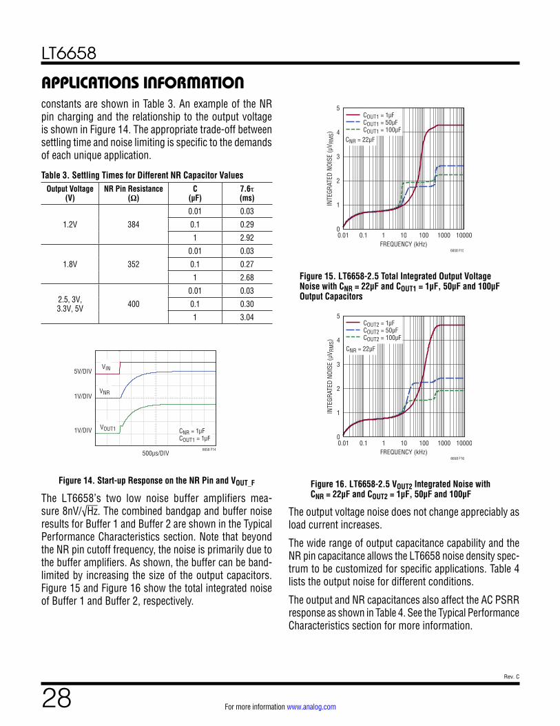
The LT6658’s two low noise buffer amplifiers mea-sure 8nV/√Hz. The combined bandgap and buffer noise results for Buffer 1 and Buffer 2 are shown in the Typical Performance Characteristics section. Note that beyond the NR pin cutoff frequency, the noise is primarily due to the buffer amplifiers. As shown, the buffer can be band-limited by increasing the size of the output capacitors. Figure 15 and Figure 16 show the total integrated noise of Buffer 1 and Buffer 2, respectively.
CNR = 22µF
COUT1 = 1µFCOUT1 = 50µFCOUT1 = 100µF
FREQUENCY (kHz)0.01 0.1 1 10 100 1000 100000
1
2
3
4
5
INTE
GRAT
ED N
OISE
(µV R
MS)
6658 F15
Figure 15. LT6658-2.5 Total Integrated Output Voltage Noise with CNR = 22µF and COUT1 = 1µF, 50µF and 100µF Output Capacitors
CNR = 22µF
COUT2 = 1µFCOUT2 = 50µFCOUT2 = 100µF
FREQUENCY (kHz)0.01 0.1 1 10 100 1000 100000
1
2
3
4
5
INTE
GRAT
ED N
OISE
(µV R
MS)
6658 F16
Figure 16. LT6658-2.5 VOUT2 Integrated Noise with CNR = 22µF and COUT2 = 1µF, 50µF and 100µF
The output voltage noise does not change appreciably as load current increases.
The wide range of output capacitance capability and the NR pin capacitance allows the LT6658 noise density spec-trum to be customized for specific applications. Table 4 lists the output noise for different conditions.
The output and NR capacitances also affect the AC PSRR response as shown in Table 4. See the Typical Performance Characteristics section for more information.

LT6658
29Rev. C
For more information www.analog.com
Power Supply Rejection
The three supply pins provide flexibility to address the unique demands of each application. When connected together, the LT6658 provides excellent AC power supply rejection. Superior performance can be achieved when the supply pins are independently powered. For example, use a separate supply for the VIN pin to isolate the bandgap circuit from the outputs. Further, each buffer can be sup-plied independently to provide a high degree of isolation as summarized in Table 3.
Output Disable
The OD pin disables the output stage of both output buf-fers. This pin is useful for disabling the buffers when fault conditions exist. For example, if external circuitry senses that the load is too hot or there is a short circuit condition, this pin can be asserted to remove the output current. This active low pin will disable the output buffers when the voltage on the pin is less than 0.8V. When the input voltage is greater than 2V the LT6658 is enabled.
APPLICATIONS INFORMATION
The start-up after enabling the LT6658 enables is deter-mined by the size of the output and NR capacitors. Figure 17 is an example of the LT6658-2.5 being enabled and disabled. The OD pin has an internal pull-up current that will keep the output buffers enabled when the OD pin floats. In noisy environments, it is recommended that OD be tied high explicitly.
OD
VOUT2
VOUT1
COUT1 = 1µFCOUT2 = 1µF
500µs/DIV
5V/DIV
1V/DIV
1V/DIV
6658 F17
Figure 17. The Output Disable Function
Table 4. Output Noise and Ripple Rejection Typical ValuesPARAMETER CONDITIONS TYP UNITSOutput Noise Voltage (VOUT1 and VOUT2)
Frequency = 10Hz, COUT = 1µF, CNR = 0F, ILOAD = Full Current* Frequency = 10Hz, COUT = 1µF, CNR = 10µF, ILOAD = Full Current* Frequency = 1kHz, COUT = 1µF, CNR = 0F, ILOAD = Full Current* Frequency = 1kHz, COUT = 1µF, CNR = 10μF, ILOAD = Full Current*
176 164 157 9
nV/√Hz nV/√Hz nV/√Hz nV/√Hz
Output RMS Noise 10Hz to 100kHz, COUT1 = 1µF, CNR = 0F 10Hz to 100kHz, COUT1 = 1µF, CNR = 10µF 10Hz to 100kHz, COUT1 = 50µF, CNR = 22µF 10Hz to 100kHz, COUT2 = 1µF, CNR = 0F 10Hz to 100kHz, COUT2 = 1µF, CNR = 10µF 10Hz to 100kHz, COUT2 = 50µF, CNR = 22µF
26.2 1.5 0.7 21.8 1.1 0.9
ppmRMS ppmRMS ppmRMS ppmRMS ppmRMS ppmRMS
Power Supply Rejection (VIN1 = VOUT1 + 3V, VIN2 = VOUT2 + 3V)
VRIPPLE = 500mVP-P, fRIPPLE = 120Hz, ILOAD1 = 150mA, COUT1 = 1µF, CNR = 1µF VRIPPLE = 150mVP-P, fRIPPLE = 10kHz, ILOAD1 = 150mA, COUT1 = 1µF, CNR = 1µF VRIPPLE = 150mVP-P, fRIPPLE = 100kHz, ILOAD1 = 150mA, COUT1 = 1µF, CNR = 1µF VRIPPLE = 150mVP-P, fRIPPLE = 1MHz, ILOAD1 = 150mA, COUT1 = 1µF, CNR = 1µF VRIPPLE = 500mVP-P, fRIPPLE = 120Hz, ILOAD2 = 50mA, COUT2 = 1µF, CNR = 1µF VRIPPLE = 150mVP-P, fRIPPLE = 10kHz, ILOAD2 = 50mA, COUT2 = 1µF, CNR = 1µF VRIPPLE = 150mVP-P, fRIPPLE = 100kHz, ILOAD2 = 50mA, COUT2 = 1µF, CNR = 1µF VRIPPLE = 150mVP-P, fRIPPLE = 1MHz, ILOAD2 = 50mA, COUT2 = 1µF, CNR = 1µF
107 96 65 64 104 96 66 65
dB dB dB dB dB dB dB dB
* The full current for ILOAD is 150mA and 50mA for output 1 and output 2, respectively.

LT6658
30Rev. C
For more information www.analog.com
APPLICATIONS INFORMATIONInternal Protection
There are two internal protection circuits for monitoring output current and die temperature.
The output stage of each output buffer is disabled when the internal die temperature is greater than 165°C. There is 11°C of hysteresis allowing the part to return to normal operation once the die temperature drops below 154°C.
In addition, a short circuit protection feature prevents the output from supplying an unlimited load current. A fault or short on either output force pin will cause the output stage to limit the current and the output voltage will drop accordingly to the output fault condition. For example, if a 1Ω fault to ground occurs on Buffer 1, the circuit protec-tion will limit both outputs. A load fault on either buffer will affect the output of both buffers.
The OD pin may also be used with external circuitry to set a latched current limit as shown in Figure 18. The LT6108-1 provides a high-side current sense, latched comparator and a reference voltage enabling a simple latched overcurrent protection circuit. The high side
sensing shown in Figure 18 adds only 7.5mV overhead to the supply and is set to trip at 150mA. Separate supply pins on the LT6658 permit each output buffer to have a dedicated overcurrent sense circuit. The RST signal resets the latched comparator.
Power Dissipation
To maintain reliable precise and accurate performance the LT6658 junction temperature should never exceed TJMAX = 150°C. If the part is operated at the absolute maximum input voltage and maximum output currents, the MSE package will need to dissipate over 7 watts of power.
The LT6658 comes in an MSE package with an exposed pad. The thermal resistance junction to case, θJC, of the MSE package is 10°C/W. The thermal resistance junction to ambient, θJA, is determined by the amount of copper on the PCB that is soldered to the exposed pad. When following established layout guidelines the θJA can be as low as 35°C/W for the MSE package.
Figure 18. LT6658-2.5V with an Overcurrent Protection Circuit
+–
+–
6658 F27
V+
EN/RST
OUTCVOUT1_F
VOUT1_S
VOUT2_F
VOUT2_S
12
13
8
7
SENSELO
OUTA
INC
V–
SENSEHI
LT6108-110k
1µF
4k
RST
VOUT2
0.1µFOC
1µFVOUT1
0.1µF
1µF
BYPASS NR GND
VIN1
10 1114
53
VIN
1µF
400ΩBANDGAP
LT6658-2.5
OD9
0.1µF 0.05Ω
75Ω5.1V TO 36V
VIN2
1, 2, 6, 17

LT6658
31Rev. C
For more information www.analog.com
As a simple example, if 2 watts are dissipated in the MSE package, the die temperature would rise 70°C above the ambient temperature. The following expression describes the rise in temperature (θJA • PTOTAL), and the increase of junction temperature over ambient temperature as
TJ = TA + θJA • PTOTAL
where TJ is the junction temperature, TA is the ambi-ent temperature, θJA is the thermal resistance junction to ambient, and PTOTAL is the total power dissipated in the LT6658. Further, if the package was initially at room temperature (25°C), the die would increase to 95°C. At 3 watts the die would exceed the specified H-grade tem-perature of 125°C.
The derating curve for the MSE package is shown in Figure 19. Three different θJA curves are shown. θJA is dependent on the amount of copper soldered to the exposed pad. Multiple layers of copper with multiple vias is recommended.
θJA = 35°C/WθJA = 60°C/WθJA = 85°C/W
TEMPERATURE (°C)0 25 50 75 100 125
0
1
2
3
MAX
. POW
ER D
ISSI
PATI
ON (W
)
6658 F18
Figure 19. MSE Derating Curve
The power dissipated by the LT6658 can be calculated as three components. There is the power dissipated in the two output devices (one for each buffer) and the power dissipated within the remaining internal circuits. Calculate the power in the remaining circuits using the following expressions
PSTATIC = VIN • ISTATIC
APPLICATIONS INFORMATIONwhere PSTATIC is the power dissipated in the LT6658 minus the output devices, VIN is the supply voltage, and ISTATIC is the current flowing through the LT6658. To cal-culate the power dissipated by the output devices use
P1 = (VIN1 – VOUT1) • IOUT1
P2 = (VIN2 – VOUT2) • IOUT2
where P1 and P2 are the power dissipated in the Buffer 1 and Buffer 2 output devices, VIN1 and VIN2 are the supply voltages for each buffer, and VOUT1 and VOUT2 are the output voltages. Finally,
PTOTAL = P1 + P2 + PSTATIC
where PTOTAL is the total power dissipated in the package. PSTATIC tends to be much smaller than P1 or P2.
To lower the power in the output devices, the supply volt-age for each of the output buffers can be reduced to only 2.5V above the output voltage. For example, with a 2.5V output, using a 5V supply and maximum output current on each buffer, the total power can be calculated as
P1 = (5V – 2.5V) • 0.15A = 0.375W
P2 = (5V – 2.5V) • 0.05A = 0.125W
PSTATIC = 5V • 0.001A = 0.005W
PTOTAL = 0.375W + 0.125W + 0.005W = 0.505W
which is an operating condition that can be tolerated above 100°C when proper heat sinking is used.
In Figure 20, the output current in both buffers is increased linearly for three values of VIN where all three supply pins are connected together. As VIN and IOUT increases, the total power increases proportionally. When the supply voltage is 30V and the total output current is 200mA, the power exceeds 5W, representing a junction temperature increase of over 175°C using a best case scenario when using a MSE with a θJA = 35°C/W. Figure 21 illustrates how rapidly power increases when the supply voltage increases, especially with 200mA of total load current. If possible, reduce the voltage on VIN1 and VIN2, which in turn will reduce the power dissipated in the LT6658 package.

LT6658
32Rev. C
For more information www.analog.com
APPLICATIONS INFORMATIONThe LT6658 is a high performance reference and extreme thermal cycling will cause thermal hysteresis and should be avoided if possible. See the Thermal Hysteresis section.
OUTPUT CURRENT (A)0
POW
ER (W
)
6
5
4
3
2
1
00.14 0.16 0.180.06
6658 F19
0.20.08 0.1 0.120.040.02
VIN = 5VVIN = 15VVIN = 30V
Figure 20. Power Dissipation vs Output Current
When the supply voltage, VIN1 or VIN2, is greater than 30V, a hard short from either output to ground can result in more than 3 to 6 watts of instantaneous power which can damage the output devices.
SUPPLY VOLTAGE (V)0
POW
ER (W
)
7
6
5
4
3
2
1
03515
6658 F20
4020 25 30105
200mANO LOAD
Figure 21. Power Dissipation vs Supply Voltage
Safe Operating Area
The safe operating area, or SOA, describes the operating region where the junction temperature does not exceed TJMAX. In Figure 22, the SOA for the LT6658 is plotted. In this plot, the output voltage is 2.5V and the output cur-rent is the combined current of both buffers. The SOA is
plotted for three values of θJA. This illustrates how a lower θJA value will remove more heat and allow more power to be dissipated through the package without damaging the part.
SUPPLY VOLTAGE – LOAD VOLTAGE (V)
LOAD
CUR
RENT
(mA)
6658 F21
1000
100
10
11 10 100
θJA = 35°C/WθJA = 60°C/WθJA = 85°C/W
TA = 25°C
Figure 22. SOA for the LT6658
There are three regions in the SOA plot. The top left region is the maximum rated current of the LT6658. The diagonal lines in the middle are where both the load current and supply voltage must be reduced as not to exceed TJMAX. The bottom right is the maximum voltage of the LT6658.
It is important to realize the SOA limit is an absolute maxi-mum rating at TJMAX. It is not recommended to operate at this limit for extended periods of time.
PCB Layout
The LT6658 is a high performance reference and there-fore, requires good layout practices. Each supply pin should have 0.1µF capacitor placed close to the package. The output capacitors should also be close to the part to keep the equivalent series resistance to a minimum. As mentioned earlier, avoid parasitic resistance between the sense line and the load. Any error here will directly affect the output voltage.
All three ground pins (1, 2, 6) , and exposed pad should be connected together, preferably in a star ground con-figuration or ground plane. The exposed pad, Pin 17, is electrically connected to the die and must be connected to ground. It is also necessary for good thermal conductivity; use plenty of copper and multiple vias.

LT6658
33Rev. C
For more information www.analog.com
APPLICATIONS INFORMATIONIf the design requires the part to dissipate significant power, consider using 2oz copper and/or a multilayer board with a large area of copper connected to the exposed pad. Note that θJA is proportional to the amount of copper soldered to the exposed pad. Preferably the copper should be on the outermost layers of the board for good thermal dissipation. A sample layout is shown in Figure 23a. The sense lines, VOUT1_S and VOUT2_S should connect as close as possible to the top of the load. In Figure 23b, a star ground is shown where the LT6658 ground is directly connected to the bottom of the load. Connect all other grounds in the system to this same point. Minimize the resistance between GND side of the load and the LT6658 GND pins, especially for applications where the LT6658 is sinking current. This minimizes load regulation errors.
LT6658-2.5
(a) LT6658 Sample PCB Layout
(b) Bring Out Ground to the Load and Make a Star Connection
+–
RLOAD
VOUT2_F
VOUT2_S
12
1, 2, 6, 17
10, 11, 14
13
VIN, VIN1, VIN2
GND
5VTO 36V
STAR-GROUND6658 F22
Figure 23.
Long Term Drift
Long term drift is a settling of the output voltage while the part is powered up. The output slowly drifts at levels of parts per million (ppm). The first 1000 hours of being powered up sees the most shift. By the end of 3000 hours, most parts have settled and will not shift appreciably. The plot in Figure 24 is representative of the LT6658 long term drift.
TIME (HOURS)0 500 1000 1500 2000 2500 3000
–50
0
50
100
150
200
LONG
TER
M D
RIFT
(ppm
)
6658 F23
Figure 24. LT6658 Long Term Drift
IR Reflow Shift
As with many precision devices, the LT6658 will experi-ence an output shift when soldered to a PCB. This shift is caused by uneven contraction and expansion of the plastic mold compound against the die and the copper pad underneath the die. Critical devices in the circuit will experience a change of physical force or pressure, which in turn changes its electrical characteristics, resulting in subtle changes in circuit behavior. Lead free solder reflow profiles reach over 250°C, which is considerably higher than lead based solder. A typical lead free IR reflow profile is shown in Figure 25. The experimental results simulat-ing this shift are shown in Figure 26. In this experiment, LT6658 is run through an IR reflow oven once and three times.

LT6658
34Rev. C
For more information www.analog.com
MINUTES
TEM
PERA
TURE
(°C)
00
75
RAMPDOWN
tP30s
40s
tL130s
120s
150
225
300
2 4 6 8
6658 F24
10
RAMP TO150°C
380sTP = 260°C
TL = 217°CTS(MAX) = 200°C
TS = 190°C
T = 150°C
Figure 25. Lead Free Reflow Profile
MSE–16 1 CYCLE3 CYCLES
CHANGE IN OUTPUT VOLTAGE (ppm)–300 –250 –200 –150 –100 –50 0 500
2
4
6
8
10
12
14
NUM
BER
OF U
NITS
6658 F25
Figure 26. ∆VOUT1 Due to IR Reflow Shift
Thermal Hysteresis
Thermal hysteresis is caused by the same effect as IR reflow shift. However, in the case of thermal hysteresis, the temperature is cycled between its specified operat-ing extremes to simulate how the part will behave as it
experiences extreme temperature excursions and then returns to room temperature. For example, the LT6658 rated for –40°C to 125°C was repeatedly cycled between 125°C and –40°C. Figure 27 illustrates the thermal hyster-esis of the LT6658, where each time the part’s tempera-ture passed through 25°C after cold and hot excursions, the output voltage was recorded.
MAX AVG HOT CYCLE25°C TO 125°C TO 25°C
MAX AVG COLD CYCLE25°C TO –40°C TO 25°C
CHANGE IN OUTPUT VOLTAGE (ppm)–100 –75 –50 –25 0 25 50 75 1000
2
4
6
8
10
12
14
NUM
BER
OF U
NITS
6658 F26a
(a) LT6658 H-Grade (–40°C to 125°C)
MAX AVG HOT CYCLE25°C TO 85°C TO 25°C
MAX AVG COLD CYCLE25°C TO –40°C TO 25°C
CHANGE IN OUTPUT VOLTAGE (ppm)–100 –75 –50 –25 0 25 50 75 1000
2
4
6
8
10
12
14
16
18
20
22
24
NUM
BER
OF U
NITS
6658 F26b
(b) LT6658 I-Grade (–40°C to 85°C)
Figure 27. Thermal Hysteresis

LT6658
35Rev. C
For more information www.analog.com
TYPICAL APPLICATIONS200mA Reference
Single Supply Precision Data Acquisition Circuit
0.1µF
1µF
1µF
1µF
0.01Ω
0.03Ω
RLOAD
VIN5V TO 36V VOUT1_FVIN1
BYPASS
LT6658-2.5
VOUT1_S
VOUT2_F
VIN2
VOUT2_S
GND
OD
11
14
10
9
3
1, 2, 6, 17
8
7
12
13
6658 TA02
6658 TA03
1k
VCM V–
4
5
6
V+ 3
8
1
2
1k
1k
35.7Ω
3300pF
35.7Ω1k
1k
VCM
1k
0.41V
3.69V
0.41V
3.69V
4.096V
6.6V
47µF
10µF
LTC2378-20
REF/DGC
IN+REF VDD
2.5V
IN–
–3.28V
3.28V0V
6800pF
6800pF
–
+LTC6362
13.7k
21.5k
10µF
1µF
LT6658-2.5
VIN1
VIN2
VIN
OD
VOUT2_F
VOUT2_S
8
7
12
13
10
11
9
14
1, 2, 6, 17GND
BYPASS
VOUT1_F
VOUT1_S
0.1µF

LT6658
36Rev. C
For more information www.analog.com
Driving Two Code Dependent DAC Reference Inputs. Separate DAC Reference Biasing Eliminates Code Dependent Reference Current Interaction
TYPICAL APPLICATIONS Driving the a Dual ADC with Independent Voltage References
5V TO 36V
0.1µF
7.5V TO 36V
0.1µF
10µF
10µF
10k
10k
2.5V
5V
LTC2323-16
GND6658 TA04
REFOUT2
REFOUT1
REFRTN1
REFRTN2
REFINT
1µF
1µF
1µF
LT6658-2.5
VINVIN1
1411
10VOUT2_FVOUT2_S
1213
GNDBYPASS1, 2, 6, 17
VOUT1_FVOUT1_S
8VIN2
7
VREF 2.5V5V
VDD
LTC2641-16
4.7µF
REF
1
6
8
VOUT
GND
6658 TA05
1µF
0.1µF
7
5
432
CSSCLKDINCLR
VDD
LTC2641-16
REF
6VOUT
GND5
432
RPAR*
CSSCLKDINCLR
VREF 2.5V5V
4.7µF
1
8
0.1µF
7
RPAR*
5V < VIN < 36V
LT6658-2.5VIN
VIN1
VIN2
14
11
10
VOUT2_F
VOUT2_S
8
7
12
13
GND1, 2, 6, 17
VOUT1_F
VOUT1_S
BYPASS
16-BIT DAC
*RPAR IS THE PARASITIC RESISTANCE OF THE BOARD TRACE AND SHOULD BE > 0.048Ω TO MAINTAIN GOOD INL
16-BIT DAC
0.1µF

LT6658
37Rev. C
For more information www.analog.com
TYPICAL APPLICATIONS
R1 AND R2 TOLERANCE
(%)
RPAR (Ω)
ILOAD (mA)
± ERROR (mV)
1 0.05 0 35.4
1 0.05 150 42.9
0.1 0.05 0 3.5
0.1 0.05 150 11.0
0.1 0.02 150 6.5
0.1 0.01 150 5.0
R1 AND R2 TOLERANCE ERRORS ADDED ROOT-SUM-SQUARE
Common Errors for Non-Unity Gain Applications
LT6658-2.5
6658 TA06
1µF 1µF
0.1µF
BYPASS
1µF
7.5V TO 36V
KELVIN SENSE ERROR: RPAR WILL CAUSE AN ERROR VERROR = ILOAD • RPAR. CONNECT THE TOP OF R1 DIRECTLY TO THE TOP OF RLOAD. RESISTOR TOLERANCE ERROR: GAIN NETWORK ERROR CAN BE REDUCED BY USING A MATCHED RESISTOR NETWORK SUCH AS THE LT5400.
VERROR = ILOAD • RPAR
1µF
GNDGND GND
+–
+–
THERMALSHUTDOWN
BANDGAP
VIN2 VIN1VIN
VOUT2_F
VOUT1_F
VOUT2_S
VOUT1_S
14 10 11
2
3
GND17 6
12
8
13
7
R110k
R210k
ILOAD
RLOAD
RPAR
VIDEAL = 5V
1
LOAD CURRENT (mA)
Load Voltage Error Due to Parasitic Resistance
LOAD
VOL
TAGE
ERR
OR (m
V)
100
10
1
0.1-10 10 30 110 130 15050 70 90
0.1Ω0.05Ω0.01Ω

LT6658
38Rev. C
For more information www.analog.com
TYPICAL APPLICATIONS
Automotive Reference and Supply Voltage Application
1µF
1µF
1µF
1µF
0.1µF
12V BATTERY
2.5V 50mAREFERENCEVOLTAGE
5V 150mASUPPLY VOLTAGE
6658 TA07
10k
10k
LT6658-2.5
VIN
VIN1
VIN2
OD
BYPASS
14
11
10
9
3
VOUT2_F
VOUT2_S
VOUT1_F
VOUT1_S
8
7
12
13
GND1, 2, 6, 17
Scale Buffer 1 Up and Scale Buffer 2 Down
+–
+– RF1
8.76k
RIN110k
RF23.2k
RIN210k
1µF3.3V AT 150mA
1µF1.8V AT 50mA
2.5V AT 10mA1µF
VIN2VIN1
1µF
400ΩBANDGAP
LT6658-2.5
0.1µF
6658 TA12
5.8V TO 36V
VOUT1_F
VOUT1_S
VOUT2_F
VOUT2_S
12
13
8
7
BYPASS NR GND
10 1114
53
VIN
OD9
1, 2, 6, 17
VOUT2 _F = 2.5V 1+RF2RIN2
VOUT1_F = 2.5V 1–RF2 • RF1
RIN2 • RIN1

LT6658
39Rev. C
For more information www.analog.com
TYPICAL APPLICATIONS
1µF
10µF
0.1µF10µF
10µF
0.1µF
7.5V TO 36V
6658 TA08
1µF1µF
1µF1µF
LT6658-2.5
VIN1
VIN2
VIN
OD
BYPASS
11
10
14
9
3
VOUT2_F
VOUT2_S
VOUT1_F
VOUT1_S
8
7
12
13
GND GND (PAD)1, 2, 6 17
VREF+
VREF–
VIN+
VIN–
VCC
GND
LTC2440
335Ω 335Ω
335Ω
1µFVREF
+
VREF–
VIN+
VIN–
VCC
GND
LTC2440
335Ω 335Ω
335Ω
1µF
VREF+
VREF–
VIN+
VIN–
VCC
GND
LTC2440
335Ω 335Ω
335Ω
1µFVREF
+
VREF–
VIN+
VIN–
VCC
GND
LTC2440
335Ω 335Ω
335Ω
1µF
10k
2.5V
5V
10k
LTC2440 AND STRAIN GAUGE BIAS
LT6658 Biasing Multiple Strain Gauges
LT6658
40Rev. C
For more information www.analog.com
TYPICAL APPLICATIONSRecursive Reference Application (VOUT1 Supplies Power to VIN and VIN2)
Low Drift Regulator Application
Precision Low Drift ApplicationDrift = 1.5ppm/°C; –40°C to 125°C
Recursive Reference Power Supply Rejection Ratio
1µF
1µF
1µF
400Ω
1µF
10k
10k
1.5k1W
10µF
10µF
VIN
7.5V TO 36V
VOUT1_F
VIN1
BYPASS
LT6658-2.5
VOUT1_S
VOUT2_F
VIN2
BANDGAP
2.5V
VOUT2_S
GNDNR
VOUT2
VOUT15V
4.7V1N5230
1N4148
1N4148
6658 TA09a
11
8
7
12
13
531, 2, 6, 17
1014
VOUT1VOUT2THEORETICAL
FREQUENCY (kHz)0.001 0.01 0.1 1 10 1000
20
40
60
80
100
120
140
160
180
POW
ER S
UPPL
Y RE
JECT
ION
RATI
O (d
B)
6658 TA09b
1µF
1µF
1µF
1µF
400Ω
1µF
SHDN
IN
GNDOUTS
OUTF
LTC6655-2.5
VIN
5V TO 13.2V
VOUT1_F
VIN1
BYPASS
LT6658-2.5
VOUT1_S
VOUT2_F
VIN2
BANDGAP
2.5V
VOUT2_S
GND
6658 TA10a
NR
VOUT2
VOUT12.5V
14 11 10
8
7
12
13
1,2,6,1753
NRVOUT1VOUT2
TEMPERATURE (°C)–40 –20 0 20 40 60 80 100 120 140
2.498
2.499
2.500
2.501
2.502
OUTP
UT V
OLTA
GE (V
)
6658 TA10b

LT6658
41Rev. C
For more information www.analog.com
PACKAGE DESCRIPTION
MSOP (MSE16) 0213 REV F
0.53 ±0.152(.021 ±.006)
SEATINGPLANE
0.18(.007)
1.10(.043)MAX
0.17 – 0.27(.007 – .011)
TYP
0.86(.034)REF
0.50(.0197)
BSC
16
16151413121110
1 2 3 4 5 6 7 8
9
9
1 8
NOTE:1. DIMENSIONS IN MILLIMETER/(INCH)2. DRAWING NOT TO SCALE3. DIMENSION DOES NOT INCLUDE MOLD FLASH, PROTRUSIONS OR GATE BURRS. MOLD FLASH, PROTRUSIONS OR GATE BURRS SHALL NOT EXCEED 0.152mm (.006") PER SIDE4. DIMENSION DOES NOT INCLUDE INTERLEAD FLASH OR PROTRUSIONS. INTERLEAD FLASH OR PROTRUSIONS SHALL NOT EXCEED 0.152mm (.006") PER SIDE5. LEAD COPLANARITY (BOTTOM OF LEADS AFTER FORMING) SHALL BE 0.102mm (.004") MAX6. EXPOSED PAD DIMENSION DOES INCLUDE MOLD FLASH. MOLD FLASH ON E-PAD SHALL NOT EXCEED 0.254mm (.010") PER SIDE.
0.254(.010) 0° – 6° TYP
DETAIL “A”
DETAIL “A”
GAUGE PLANE
5.10(.201)MIN
3.20 – 3.45(.126 – .136)
0.889 ±0.127(.035 ±.005)
RECOMMENDED SOLDER PAD LAYOUT
0.305 ±0.038(.0120 ±.0015)
TYP
0.50(.0197)
BSC
BOTTOM VIEW OFEXPOSED PAD OPTION
2.845 ±0.102(.112 ±.004)
2.845 ±0.102(.112 ±.004)
4.039 ±0.102(.159 ±.004)
(NOTE 3)
1.651 ±0.102(.065 ±.004)
1.651 ±0.102(.065 ±.004)
0.1016 ±0.0508(.004 ±.002)
3.00 ±0.102(.118 ±.004)
(NOTE 4)
0.280 ±0.076(.011 ±.003)
REF
4.90 ±0.152(.193 ±.006)
DETAIL “B”
DETAIL “B”CORNER TAIL IS PART OF
THE LEADFRAME FEATURE.FOR REFERENCE ONLY
NO MEASUREMENT PURPOSE
0.12 REF
0.35REF
MSE Package16-Lead Plastic MSOP, Exposed Die Pad
(Reference LTC DWG # 05-08-1667 Rev F)

LT6658
42Rev. C
For more information www.analog.com
PACKAGE DESCRIPTION
3.00 ±0.10(2 SIDES)
4.00 ±0.10(2 SIDES)
NOTE:1. DRAWING PROPOSED TO BE MADE VARIATION OF VERSION (WGED-3) IN JEDEC PACKAGE OUTLINE MO-2292. DRAWING NOT TO SCALE 3. ALL DIMENSIONS ARE IN MILLIMETERS4. DIMENSIONS OF EXPOSED PAD ON BOTTOM OF PACKAGE DO NOT INCLUDE MOLD FLASH. MOLD FLASH, IF PRESENT, SHALL NOT EXCEED 0.15mm ON ANY SIDE5. EXPOSED PAD SHALL BE SOLDER PLATED6. SHADED AREA IS ONLY A REFERENCE FOR PIN 1 LOCATION ON THE TOP AND BOTTOM OF PACKAGE
0.40 ±0.10
BOTTOM VIEW—EXPOSED PAD
1.70 ±0.10
0.75 ±0.05
R = 0.115TYP
R = 0.05TYP
3.15 REF
1.70 ±0.05
18
169
PIN 1TOP MARK
(SEE NOTE 6)
0.200 REF
0.00 – 0.05
(DE16) DFN 0806 REV Ø
PIN 1 NOTCHR = 0.20 OR0.35 × 45°CHAMFER
3.15 REF
RECOMMENDED SOLDER PAD PITCH AND DIMENSIONSAPPLY SOLDER MASK TO AREAS THAT ARE NOT SOLDERED
2.20 ±0.05
0.70 ±0.05
3.60 ±0.05
PACKAGEOUTLINE
0.25 ±0.05
3.30 ±0.05
3.30 ±0.10
0.45 BSC
0.23 ±0.050.45 BSC
DE Package16-Lead Plastic DFN (4mm × 3mm)
(Reference LTC DWG # 05-08-1732 Rev Ø)

LT6658
43Rev. C
For more information www.analog.com
REVISION HISTORY
Information furnished by Analog Devices is believed to be accurate and reliable. However, no responsibility is assumed by Analog Devices for its use, nor for any infringements of patents or other rights of third parties that may result from its use. Specifications subject to change without notice. No license is granted by implication or otherwise under any patent or patent rights of Analog Devices.
REV DATE DESCRIPTION PAGE NUMBER
A 10/17 Addition of 1.2V, 1.8V, 3V, 3.3V, 5V OptionsThe term “Channel” was replaced by the term “Buffer”New Application Section “Using the BYPASS Pin as a Reference”Edits for clarification to Application Section “Output Voltage Scaling”Addition of Figure 18 and use of the OD pin to Application Section “Internal Protection”Updated Typical Application “200mA Reference”Updated Typical Application “Recursive Reference Application”
1-18, 20, 25, 26
ALL2224283337
B 07/18 Changed Load RegulationChanged VIN Minimum VoltageChanged Output Short-Circuit Current and added Note 11Corrected Table 4Corrected Typical Application circuit TA12Updated Typical Application
145
273540
C 05/19 Added 4mm × 3mm DFN package and order information Updated Note 11
1–57

LT6658
44Rev. C
For more information www.analog.com ANALOG DEVICES, INC. 2016–2019
D17045-0-05/19(c)www.analog.com
RELATED PARTS
TYPICAL APPLICATION
PART NUMBER DESCRIPTION COMMENTS
LT1460 Micropower Series References 20mA Output Drive, 0.075% Accuracy, 10ppm/°C Drift
LT1461 Precision Low Dropout Series References 50mA Output Drive, 0.04% Accuracy, 3ppm/°C Drift, 50µA Supply Current, 300mV Dropout
LT6654 All Purpose, Rugged and Precise Series References ±10mA Output Drive, 0.05% Accuracy, 10ppm/°C Drift, 100mV Dropout, 1.6ppmP-P Noise (0.1Hz to 10Hz), –55°C to 125°C
LTC6655 Precision Low Noise Series References ±5mA Output Drive, 0.025% Accuracy, 2ppm/°C Max Drift, 0.25ppmP-P Noise (0.1Hz to 10Hz), –40°C to 125°C
LT6660 Tiny Micropower Series References 20mA Output Drive, 0.2% Accuracy, 20ppm/°C Drift, 2mm × 2mm DFN Package
LT1761 Low Noise Low Dropout Linear Regulator 100mA Output Drive, 300mV Dropout, VIN = 1.8V to 20V, 20µVRMS Noise (10Hz to 100kHz), ThinSOT™ package
LT3042 Ultralow Noise, Ultrahigh PSRR Linear Regulator 200mA Output Drive, 350mV Dropout, VIN = 1.8V to 20V 0.8µVRMS Noise (10Hz to 100kHz), 79dB PSRR (1MHz)
LT3050 Low Noise Linear Regulator with Current Limit and Diagnostic Functions
100mA Output Drive, 300mV Dropout, VIN = 2V to 45V, 30μVRMS Noise (10Hz to 100kHz), 50μA Supply Current, Adj. Output
LT3060 Micropower, Low Noise, Low Dropout Linear Regulator
100mA Output Drive, 300mV Dropout, VIN =1.7V to 45V, 30μVRMS Noise (10Hz to 100kHz), 40μA Supply Current, Adj. Output
LT3063 Micropower, Low Noise, Low Dropout Linear Regulator with Output Discharge
200mA Output Drive, 300mV Dropout, VIN =1.6V to 45V, 30μVRMS Noise (10Hz to 100kHz), 40μA Supply Current
1µF
10µF
LTC6362
3300pF
6800pF
6800pF
47µF
1k
1k
1k
1k
35.7Ω
35.7Ω
21k
13.7k
10k
10k
1µF
1µF
1k
1k10µF
464Ω
400Ω
1µF
VIN
7.5V TO 36V
VOUT1_F
VIN1
BYPASS
LT6658-2.5
VOUT1_S
2.5V(X7R, 1210 SIZE)
6658 TA11
LT5400-4
VOUT2_F
VIN2
BANDGAP
5V
4.096V
VOUT2_S
GND
3.28V0V
–3.28V
TO OTHERANALOG CIRCUITS
NR
+
– +
–S
IN+
IN–
VDDREF
GNDREF/DGC
LTC2379-18VOCM
14 11 10
8
7
12
13
1,2,6,1753
Providing a Precision Reference and Supply Voltage to a Mixed Signal Application