Embed Size (px)
Citation preview

LT8390
18390fa
For more information www.linear.com/LT8390
TYPICAL APPLICATION
FEATURES DESCRIPTION
60V Synchronous 4-Switch Buck-Boost Controller
with Spread Spectrum
The LT®8390 is a synchronous 4-switch buck-boost DC/DC controller that regulates output voltage, input or output current from an input voltage above, below, or equal to the output voltage. The proprietary peak-buck/peak-boost current mode control scheme allows adjustable and syn-chronizable 150kHz to 650kHz fixed frequency operation, or internal ±15% triangle spread spectrum frequency modulation for low EMI. With a 4V to 60V input voltage range, 0V to 60V output voltage capability, and seamless low noise transitions between operation regions, the LT8390 is ideal for voltage regulator, battery and supercapacitor charger applications in automotive, industrial, telecom, and even battery-powered systems.
The LT8390 provides input or output current monitor and power good flag. Fault protection is also provided to detect output short-circuit condition, during which the LT8390 retries, latches off, or keeps running.
98% Efficient 48W (12V 4A) Miniature Buck-Boost Voltage Regulator
APPLICATIONS
n 4-Switch Single Inductor Architecture Allows VIN Above, Below or Equal to VOUT
n Synchronous Switching: Up to 98% Efficiency n Proprietary Peak-Buck Peak-Boost Current Mode n Wide VIN Range: 4V to 60V n ±1.5% Output Voltage Accuracy: 1V ≤ VOUT ≤ 60V n ±3% Input or Output Current Accuracy with Monitor n Spread Spectrum Frequency Modulation for Low EMI n High Side PMOS Load Switch Driver n Integrated Bootstrap Diodes n No Top MOSFET Refresh Noise in Buck or Boost n Adjustable and Synchronizable: 150kHz to 650kHz n VOUT Disconnected from VIN During Shutdown n Available in 28-Lead TSSOP with Exposed Pad and
28-Lead QFN (4mm × 5mm)
n Automotive, Industrial, Telecom Systems n High Power Battery-Powered System
L, LT, LTC, LTM, Linear Technology and the Linear logo are registered trademarks of Analog Devices, Inc. All other trademarks are the property of their respective owners.
Efficiency vs VIN
IOUT = 4A
INPUT VOLTAGE (V)0 10 20 30 40 50 60
86
88
90
92
94
96
98
100
EFFI
CIEN
CY (%
)
8390 TA01b
165k
0.1µF
4.7µF
4mΩ
0.1µF
6uH
22µF
383k
4.7µF 100k
0.47µF
100k
4.7nF
27k
100k
9.09k
15mΩ
10µF25V×2
0.1µF
1µF 1µF
100pF
120µF16V
120µF16V
EN/UVLO
VREF
CTRL
PGOOD
BG2
BST2
TG2
INTVCC
LOADEN
FB
VOUT
ISP
ISN
SYNC/SPRD
TEST
VIN4V TO 56V
400kHz
63V×2
100V×2
ISMON
PGOOD
VOUT12V4A
LSP LSNSW1 SW2BST1
TG1
BG1
VIN LT8390
LOADTG
ISMON
SS VC RT
GND
SSFM OFF
SSFM ONIOUT LIMIT 6.7A
8390 TA01a

LT8390
28390fa
For more information www.linear.com/LT8390
ABSOLUTE MAXIMUM RATINGSVIN, EN/UVLO, VOUT, ISP, ISN ....................................60V(ISP-ISN) ..........................................................–1V to 1VBST1, BST2 ................................................................66VSW1, SW2, LSP, LSN ..................................... –6V to 60VINTVCC, (BST1-SW1), (BST2-SW2) ..............................6V(BST1-LSP), (BST1-LSN) .............................................6V
(Note 1)
ORDER INFORMATIONLEAD FREE FINISH TAPE AND REEL PART MARKING* PACKAGE DESCRIPTION TEMPERATURE RANGE
LT8390EFE#PBF LT8390EFE#TRPBF LT8390FE 28-Lead Plastic TSSOP –40°C to 125°C
LT8390IFE#PBF LT8390IFE#TRPBF LT8390FE 28-Lead Plastic TSSOP –40°C to 125°C
LT8390HFE#PBF LT8390HFE#TRPBF LT8390FE 28-Lead Plastic TSSOP –40°C to 150°C
LT8390EUFD#PBF LT8390EUFD#TRPBF 8390 28-Lead (4mm × 5mm) Plastic QFN –40°C to 125°C
LT8390IUFD#PBF LT8390IUFD#TRPBF 8390 28-Lead (4mm × 5mm) Plastic QFN –40°C to 125°C
LT8390HUFD#PBF LT8390HUFD#TRPBF 8390 28-Lead (4mm × 5mm) Plastic QFN –40°C to 150°C
Consult LTC Marketing for parts specified with wider operating temperature ranges. *The temperature grade is identified by a label on the shipping container.For more information on lead free part marking, go to: http://www.linear.com/leadfree/ For more information on tape and reel specifications, go to: http://www.linear.com/tapeandreel/. Some packages are available in 500 unit reels through designated sales channels with #TRMPBF suffix.
1
2
3
4
5
6
7
8
9
10
11
12
13
14
TOP VIEW
FE PACKAGE28-LEAD PLASTIC TSSOP
28
27
26
25
24
23
22
21
20
19
18
17
16
15
BG1
BST1
SW1
TG1
LSP
LSN
VIN
INTVCC
EN/UVLO
TEST
LOADEN
VREF
CTRL
ISP
BG2
BST2
SW2
TG2
VOUT
LOADTG
SYNC/SPRD
RT
VC
FB
SS
PGOOD
ISMON
ISN
29GND
θJA = 30°C/W, θJC = 5°C/W
EXPOSED PAD (PIN 29) IS GND, MUST BE SOLDERED TO PCB
9 10
TOP VIEW
29GND
UFD PACKAGE28-LEAD (4mm × 5mm) PLASTIC QFN
11 12 13
28 27 26 25 24
14
23
6
5
4
3
2
1TG1
LSP
LSN
VIN
INTVCC
EN/UVLO
TEST
LOADEN
TG2
VOUT
LOADTG
SYNC/SPRD
RT
VC
FB
SSSW
1
BST1
BG1
BG2
BST2
SW2
V REF
CTRL IS
P
ISN
ISM
ON
PGOO
D
7
17
18
19
20
21
22
16
8 15
θJA = 43°C/W, θJC = 3.4°C/W
EXPOSED PAD (PIN 29) IS GND, MUST BE SOLDERED TO PCB
PIN CONFIGURATION
http://www.linear.com/product/LT8390#orderinfo
FB, LOADEN, SYNC/SPRD, CTRL, PGOOD ...................6VOperating Junction Temperature Range (Notes 2, 3)
LT8390E ............................................. –40°C to 125°C LT8390I .............................................. –40°C to 125°C LT8390H ............................................. –40°C to 150°C
Storage Temperature Range ................... –65°C to 150°C

LT8390
38390fa
For more information www.linear.com/LT8390
ELECTRICAL CHARACTERISTICS The l denotes the specifications which apply over the full operating temperature range, otherwise specifications are at TA = 25°C (Note 2). VIN = 12V, VEN/UVLO = 1.5V unless otherwise noted.
PARAMETER CONDITIONS MIN TYP MAX UNITSSupplyVIN Operating Voltage Range l 4 60 VVIN Quiescent Current VEN/UVLO = 0.3V
VEN/UVLO = 1.1V Not Switching
1 270 2.1
2
2.8
µA µA
mAVOUT Voltage Range l 0 60 VVOUT Quiescent Current VEN/UVLO = 0.3V, VOUT = 12V
VEN/UVLO = 1.1V, VOUT = 12V Not Switching, VOUT = 12V
20
0.1 0.1 40
0.5 0.5 60
µA µA µA
Linear RegulatorsINTVCC Regulation Voltage IINTVCC = 20mA 4.85 5.0 5.15 VINTVCC Load Regulation IINTVCC = 0mA to 80mA 1 4 %INTVCC Line Regulation IINTVCC = 20mA, VIN = 6V to 60V 1 4 %INTVCC Current Limit VINTVCC = 4.5V 80 110 160 mAINTVCC Dropout Voltage (VIN – INTVCC) IINTVCC = 20mA, VIN = 4V 160 mVINTVCC Undervoltage Lockout Threshold Falling 3.44 3.54 3.64 VINTVCC Undervoltage Lockout Hysteresis 0.24 VVREF Regulation Voltage IVREF = 100µA l 1.97 2.00 2.03 VVREF Load Regulation IVREF = 0mA to 1mA 0.4 1 %VREF Line Regulation IVREF = 100µA, VIN = 4V to 60V 0.1 0.2 %VREF Current Limit VREF = 1.8V 2 2.5 3.2 mAVREF Undervoltage Lockout Threshold Falling 1.78 1.84 1.90 VVREF Undervoltage Lockout Hysteresis 50 mVControl Inputs/OutputsEN/UVLO Shutdown Threshold l 0.3 0.6 1.0 VEN/UVLO Enable Threshold Falling l 1.196 1.220 1.244 VEN/UVLO Enable Hysteresis 13 mVEN/UVLO Hysteresis Current VEN/UVLO = 0.3V
VEN/UVLO = 1.1V VEN/UVLO = 1.3V
–0.1 2.2
–0.1
0 2.5 0
0.1 2.8 0.1
µA µA µA
CTRL Input Bias Current VCTRL = 0.75V, Current Out of Pin 0 20 50 nACTRL Latch-Off Threshold Falling l 285 300 315 mVCTRL Latch-Off Hysteresis 25 mVLoad Switch DriverLOADEN Threshold Rising l 1.3 1.4 1.5 VLOADEN Hysteresis 220 mVMinimum VOUT for LOADTG to be On VLOADEN = 5V 2.4 3 V LOADTG On Voltage V(VOUT-LOADTG) VOUT = 12V 4.6 5 5.4 V LOADTG Off Voltage V(VOUT-LOADTG) VOUT = 12V –0.1 0 0.1 V LOADEN to LOADTG Turn On Propagation Delay LOADEN to LOADTG Turn Off Propagation Delay
CLOADTG = 3.3nF to VOUT, 50% to 50% CLOADTG = 3.3nF to VOUT, 50% to 50%
90 40
ns ns
LOADTG Turn On Fall Time LOADTG Turn Off Rise Time
CLOADTG = 3.3nF to VOUT, 10% to 90% CLOADTG = 3.3nF to VOUT, 90% to 10%
300 10
ns ns

LT8390
48390fa
For more information www.linear.com/LT8390
ELECTRICAL CHARACTERISTICS The l denotes the specifications which apply over the full operating temperature range, otherwise specifications are at TA = 25°C (Note 2). VIN = 12V, VEN/UVLO = 1.5V unless otherwise noted.
PARAMETER CONDITIONS MIN TYP MAX UNITSError AmplifierFull Scale Current Regulation V(ISP-ISN) VCTRL = 2V, VISP = 12V
VCTRL = 2V, VISP = 0Vl
l
97 97
100 100
103 103
mV mV
1/10th Current Regulation V(ISP-ISN) VCTRL = 0.35V, VISP = 12V VCTRL = 0.35V, VISP = 0V
l
l
8 8
10 10
12 12
mV mV
ISMON Monitor Output VISMON V(ISP-ISN) = 100mV, VISP = 12V/0V V(ISP-ISN) = 10mV, VISP = 12V/0V V(ISP-ISN) = 0mV, VISP = 12V/0V
l
l
l
1.20 0.30 0.20
1.25 0.35 0.25
1.30 0.40 0.30
V V V
ISP/ISN Input Common Mode Range l 0 60 VISP/ISN Low Side to High Side Switchover Voltage VISP = VISN 1.8 VISP/ISN High Side to Low Side Switchover Voltage VISP = VISN 1.7 VISP Input Bias Current VLOADEN = 5V, VISP = VISN = 12V
VLOADEN = 5V, VISP = VISN = 0V VEN/UVLO = 0V, VISP = VISN = 12V or 0V
23 –10 0
µA µA µA
ISN Input Bias Current VLOADEN = 5V, VISP = VISN = 12V VLOADEN = 5V, VISP = VISN = 0V VEN/UVLO = 0V, VISP = VISN = 12V or 0V
23 –10 0
µA µA µA
ISP/ISN Current Regulation Amplifier gm 2000 µsFB Regulation Voltage VC = 1.2V l 0.985 1.00 1.015 VFB Line Regulation VIN = 4V to 60V 0.2 0.5 %FB Load Regulation 0.2 0.8 %FB Voltage Regulation Amplifier gm 660 µSFB Input Bias Current FB in Regulation, Current Out of Pin 10 40 nAVC Output Impedance 10 MΩ VC Standby Leakage Current VC = 1.2V, VLOADEN = 0V –10 0 10 nACurrent ComparatorMaximum Current Sense Threshold V(LSP-LSN) Buck, VFB = 0.8V
Boost, VFB = 0.8Vl
l
35 40
50 50
65 60
mV mV
Reverse Current Sense Threshold V(LSP-LSN) Buck, VFB = 0.8V Boost, VFB = 0.8V
1 1
mV mV
LSP Pin Bias Current VLSP = VLSN = 12V 60 µA LSN Pin Bias Current VLSP = VLSN = 12V 60 µAFaultFB Overvoltage Threshold (VFB) Rising l 1.08 1.1 1.12 VFB Overvoltage Hysteresis l 35 50 65 mVFB Short Threshold (VFB) Falling l 0.24 0.25 0.26 VFB Short Hysteresis Hysteresis l 35 50 65 mVISP/ISN Over Current Threshold V(ISP-ISN) VISP = 12V 750 mVPGOOD Upper Threshold Offset from VFB Rising l 8 10 12 %PGOOD Lower Threshold Offset from VFB Falling l –12 –10 –8 %PGOOD Pull-Down Resistance 100 200 Ω SS Hard Pull-Down Resistance VEN/UVLO = 1.1V 100 200 ΩSS Pull-Up Current VFB = 0.4V, VSS = 0V 10.5 12.5 14.5 µASS Pull-Down Current VFB = 0.1V, VSS = 2V 1.05 1.25 1.45 µA

LT8390
58390fa
For more information www.linear.com/LT8390
ELECTRICAL CHARACTERISTICS The l denotes the specifications which apply over the full operating temperature range, otherwise specifications are at TA = 25°C (Note 2). VIN = 12V, VEN/UVLO = 1.5V unless otherwise noted.
PARAMETER CONDITIONS MIN TYP MAX UNITSSS Fault Latch-Off Threshold 1.7 VSS Fault Reset Threshold 0.2 VOscillatorRT Pin Voltage RT = 100kΩ 1.00 V Switching Frequency VSYNC/SPRD = 0V, RT = 226kΩ
VSYNC/SPRD = 0V, RT = 100kΩ VSYNC/SPRD = 0V, RT = 59.0kΩ
l
l
l
190 380 570
200 400 600
210 420 630
kHz kHz kHz
SYNC Frequency 150 650 kHz SYNC/SPRD Input Bias Current VSYNC/SPRD = 5V –0.1 0 0.1 µA SYNC/SPRD Threshold Voltage 0.4 1.5 VHighest Spread Spectrum Above Oscillator Frequency VSYNC/SPRD = 5V 12.5 14.5 16.5 %Lowest Spread Spectrum Below Oscillator Frequency VSYNC/SPRD = 5V –17.7 –15.7 –13.7 %Region TransitionBuck-Boost to Boost (VIN/VOUT) 0.73 0.75 0.77 Boost to Buck-Boost (VIN/VOUT) 0.83 0.85 0.87 Buck to Buck-Boost (VIN/VOUT) 1.16 1.18 1.20 Buck-Boost to Buck (VIN/VOUT) 1.31 1.33 1.35 Peak-Buck to Peak-Boost (VIN/VOUT) 0.96 0.98 1.00 Peak-Boost to Peak-Buck (VIN/VOUT) 1.00 1.02 1.04 NMOS DriversTG1, TG2 Gate Driver On-Resistance Gate Pull-Up Gate Pull-Down
V(BST-SW) = 5V 2.6 1.4
Ω Ω
BG1, BG2 Gate Driver On-Resistance Gate Pull-Up Gate Pull-Down
VINTVCC = 5V 3.2 1.2
Ω Ω
TG1, TG2 Rise Time TG1, TG2 Fall Time
CL = 3.3nF, 10% to 90% CL = 3.3nF, 90% to 10%
25 20
ns ns
BG1, BG2 Rise Time BG1, BG2 Fall Time
CL = 3.3nF, 10% to 90% CL = 3.3nF, 90% to 10%
25 20
ns ns
TG Off to BG On Delay CL = 3.3nF 60 nsBG Off to TG On Delay CL = 3.3nF 60 nsTG1 Minimum Duty Cycle in Buck Region Peak-Buck Current Mode 10 %TG1 Maximum Duty Cycle in Buck Region Peak-Buck Current Mode 95 %TG1 Fixed Duty Cycle in Buck-Boost Region Peak-Boost Current Mode 85 %BG2 Fixed Duty Cycle in Buck-Boost Region Peak-Buck Current Mode 15 %BG2 Minimum Duty Cycle in Boost Region Peak-Boost Current Mode 10 %BG2 Maximum Duty Cycle in Boost Region Peak-Boost Current Mode 95 %
Note 1: Stresses beyond those listed under Absolute Maximum Ratings may cause permanent damage to the device. Exposure to any Absolute Maximum Rating condition for extended periods may affect device reliability and lifetime.Note 2: The LT8390E is guaranteed to meet performance specifications from 0°C to 125°C operating junction temperature. Specifications over the –40°C to 125°C operating junction temperature range are assured by design, characterization and correlation with statistical process controls. The LT8390I is guaranteed over the –40°C to 125°C operating junction
temperature range. The LT8390H is guaranteed over the –40°C to 150°C operating junction temperature range. High junction temperatures degrade operating lifetimes. Operating lifetime is derated at junction temperatures greater than 125°C.Note 3: The LT8390 includes overtemperature protection that is intended to protect the device during momentary overload conditions. Junction temperature will exceed 150°C when overtemperature protection is active. Continuous operation above the specified absolute maximum operating junction temperature may impair device reliability.

LT8390
68390fa
For more information www.linear.com/LT8390
TYPICAL PERFORMANCE CHARACTERISTICS
Efficiency vs Load Current (Buck Region)
Efficiency vs Load Current (Buck-Boost Region)
Efficiency vs Load Current (Boost Region)
TA = 25°C, unless otherwise noted.
Switching Waveforms (Buck Region)
Switching Waveforms (Buck-Boost Region)
Switching Waveforms (Boost Region)
VOUT vs IOUT (CV/CC) VIN Shutdown Current VIN Quiescent Current
FRONT PAGE APPLICATIONVIN = 24V, VOUT = 12V, fSW = 400kHz
LOAD CURRENT (A)0 0.5 1 1.5 2 2.5 3 3.5 4
40
50
60
70
80
90
100
EFFI
CIEN
CY (%
)
8390 G01
FRONT PAGE APPLICATIONVIN = 12V, VOUT = 12V, fSW = 400kHz
LOAD CURRENT (A)0 0.5 1 1.5 2 2.5 3 3.5 4
40
50
60
70
80
90
100
EFFI
CIEN
CY (%
)
8390 G02
FRONT PAGE APPLICATIONVIN = 5V, VOUT = 12V, fSW = 400kHz
LOAD CURRENT (A)0 0.5 1 1.5 2 2.5 3 3.5 4
40
50
60
70
80
90
100
EFFI
CIEN
CY (%
)
8390 G03
1µs/DIVFRONT PAGE APPLICATIONVIN = 18V, IOUT = 3A
VSW110V/DIV
VSW210V/DIV
IL2A/DIV
VOUT500mV/DIV
8390 G041µs/DIV
FRONT PAGE APPLICATIONVIN = 12V, IOUT = 3A
VSW110V/DIV
VSW210V/DIV
IL2A/DIV
VOUT500mV/DIV
8390 G05 1µs/DIVFRONT PAGE APPLICATIONVIN = 8V, IOUT = 3A
VSW110V/DIV
VSW210V/DIV
IL2A/DIV
VOUT500mV/DIV
8390 G06
LOAD CURRENT (A)0 1 2 3 4 5 6
0
2
4
6
8
10
12
14
OUTP
UT V
OLTA
GE (V
)
8390 G07TEMPERATURE (°C)
–500.0
I Q (µ
A)
2.5
2.0
1.5
1.0
0.5
3.0
125100 150–25 0 25
8390 G08
7550
VIN = 60V
VIN = 12V
VIN = 4V
TEMPERATURE (°C)–50
1.8
I Q (m
A)
2.6
2.4
2.2
2.0
2.8
125100 150–25 0 25
8390 G09
7550
VIN = 60V
VIN = 12V
VIN = 4V

LT8390
78390fa
For more information www.linear.com/LT8390
TYPICAL PERFORMANCE CHARACTERISTICS TA = 25°C, unless otherwise noted.
INTVCC Voltage vs Temperature INTVCC Voltage vs VIN INTVCC UVLO Threshold
VREF Voltage vs Temperature VREF Voltage vs VIN VREF UVLO Threshold
EN/UVLO Enable Threshold EN/UVLO Hysteresis Current CTRL Latch-Off Threshold
TEMPERATURE (°C)–50
4.85
V INT
VCC
(V )
5.10
5.05
5.00
4.95
4.90
5.15
125100 150–25 0 25
8390 G10
7550
IINTVCC = 0mA
IINTVCC = 80mA
VIN (V)0
4.85
V INT
VCC
(V)
5.10
5.05
5.00
4.95
4.90
5.15
5040 6010 20
8390 G11
30
IINTVCC = 20mA
TEMPERATURE (°C)–50
3.2
V INT
VCC
(V)
3.8
3.9
3.7
3.5
3.6
3.4
3.3
4.0
125100 150–25 0 25 50
8390 G12
75
RISING
FALLING
TEMPERATURE (°C)–50
1.96
V REF
(V)
2.02
2.03
2.01
1.99
2.00
1.98
1.97
2.04
125100 150–25 0 25 50
8390 G13
75
IVREF = 0mA
IVREF = 1mA
VIN (V)0
1.96
V REF
(V)
2.02
2.03
2.01
1.99
2.00
1.98
1.97
2.04
5040 6010 20
8390 G14
30
IVREF = 100µA
TEMPERATURE (°C)–50
1.70
V REF
(V)
1.90
1.95
1.85
1.80
1.75
2.00
125100 150–25 250 50
8390 G15
75
RISING
FALLING
TEMPERATURE (°C)–50
1.200
V EN/
UVLO
(V)
1.230
1.235
1.225
1.220
1.215
1.210
1.205
1.240
125100 150–25 250 50
8390 G16
75
RISING
FALLING
TEMPERATURE (°C)–50
2.0
I HYS
(µA)
2.8
2.6
2.4
2.2
3.0
125100 150–25 250 50
8390 G17
75
RISING
FALLING
TEMPERATURE (°C)–50 –25 0 25 50 75 100 125 150
0.20
0.25
0.30
0.35
0.40
V CTR
L (V
)
8390 G18

LT8390
88390fa
For more information www.linear.com/LT8390
TYPICAL PERFORMANCE CHARACTERISTICS
V(ISP-ISN) Regulation vs VCTRL V(ISP-ISN) Regulation vs VISP
V(ISP-ISN) Regulation vs Temperature
TA = 25°C, unless otherwise noted.
V(ISP-ISN) Regulation vs VFB FB Regulation vs TemperatureMaximum Current Sense vs Temperature
FB Overvoltage Threshold FB Short Threshold PGOOD Thresholds
VCTRL (V)0 0.25 0.50 0.75 1 1.25 1.50 1.75 2
0
25
50
75
100
125
V (IS
P-IS
N) (m
V)
8390 G19VISP (V)
094
V (IS
P-IS
N) (m
V) 102
104
100
98
96
106
5040 6010 20
8390 G20
30TEMPERATURE (°C)
–50 –2594
V (IS
P-IS
N) (m
V) 102
104
100
98
96
106
125100 1500 25
8390 G21
7550
ISP = 60VISP = 12VISP = 0V
VFB (V)0.96 0.970
V (IS
P-IS
N) (m
V) 80
100
60
40
20
120
1.031.02 1.040.98 0.99
8390 G22
1.011.00TEMPERATURE (°C)
–50 –250.97
V FB
(V)
1.01
1.02
1.00
0.99
0.98
1.03
125100 1500 25
8390 G23
7550
VIN = 60VVIN = 12VVIN = 4V
TEMPERATURE (°C)–50 –25
30
CURR
ENT
LIM
IT (m
V)
60
65
55
50
45
40
35
70
125100 1500 25
8390 G24
7550
BOOSTBUCK
RISING
FALLING
TEMPERATURE (°C)–50 –25 0 25 50 75 100 125 150
0.90
0.95
1.00
1.05
1.10
1.15
1.20
V FB
(V)
8390 G25TEMPERATURE (°C)
–50 –250.10
V FB
(V)
0.30
0.35
0.25
0.20
0.15
0.40
125100 1500 25
8390 G26
7550
RISING
FALLING
UPPER RISING
UPPER FALLING
LOWER RISING
LOWER FALLING
TEMPERATURE (°C)–50 –25 0 25 50 75 100 125 150
–20
–15
–10
–5
0
5
10
15
20
THRE
SHOL
D OF
FSET
(%)
8390 G27

LT8390
98390fa
For more information www.linear.com/LT8390
TYPICAL PERFORMANCE CHARACTERISTICS TA = 25°C, unless otherwise noted.
ISMON Voltage vs V(ISP-ISN) SS Current vs TemperatureOscillator Frequency vs Temperature
V(ISP-ISN) (mV)0 20 40 60 80 100
0
0.25
0.50
0.75
1.00
1.25
1.50
V ISM
ON (V
)
8390 G28TEMPERATURE (°C)
–50 –250.0
I SS
(µA)
10.0
12.5
7.5
5.0
2.5
15.0
125100 1500 25
8390 G29
7550
PULL-UP
PULL-DOWN
TEMPERATURE (°C)–50 –25
100
SWIT
CHIN
G FR
EQUE
NCY
(kHz
)
500
600
400
300
200
700
125100 1500 25
8390 G30
7550
RT = 59.0k
RT = 100k
RT = 226k
LT8390
108390fa
For more information www.linear.com/LT8390
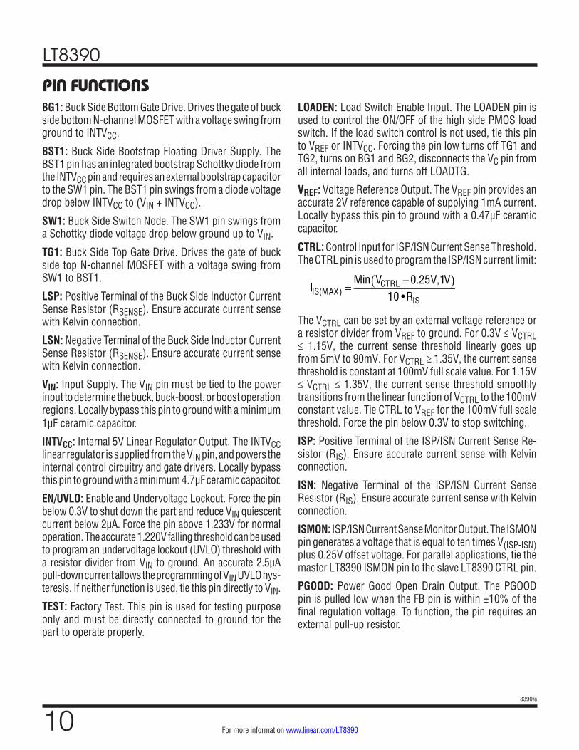
PIN FUNCTIONSBG1: Buck Side Bottom Gate Drive. Drives the gate of buck side bottom N-channel MOSFET with a voltage swing from ground to INTVCC.
BST1: Buck Side Bootstrap Floating Driver Supply. The BST1 pin has an integrated bootstrap Schottky diode from the INTVCC pin and requires an external bootstrap capacitor to the SW1 pin. The BST1 pin swings from a diode voltage drop below INTVCC to (VIN + INTVCC).
SW1: Buck Side Switch Node. The SW1 pin swings from a Schottky diode voltage drop below ground up to VIN.
TG1: Buck Side Top Gate Drive. Drives the gate of buck side top N-channel MOSFET with a voltage swing from SW1 to BST1.
LSP: Positive Terminal of the Buck Side Inductor Current Sense Resistor (RSENSE). Ensure accurate current sense with Kelvin connection.
LSN: Negative Terminal of the Buck Side Inductor Current Sense Resistor (RSENSE). Ensure accurate current sense with Kelvin connection.
VIN: Input Supply. The VIN pin must be tied to the power input to determine the buck, buck-boost, or boost operation regions. Locally bypass this pin to ground with a minimum 1µF ceramic capacitor.
INTVCC: Internal 5V Linear Regulator Output. The INTVCC linear regulator is supplied from the VIN pin, and powers the internal control circuitry and gate drivers. Locally bypass this pin to ground with a minimum 4.7µF ceramic capacitor.
EN/UVLO: Enable and Undervoltage Lockout. Force the pin below 0.3V to shut down the part and reduce VIN quiescent current below 2µA. Force the pin above 1.233V for normal operation. The accurate 1.220V falling threshold can be used to program an undervoltage lockout (UVLO) threshold with a resistor divider from VIN to ground. An accurate 2.5µA pull-down current allows the programming of VIN UVLO hys-teresis. If neither function is used, tie this pin directly to VIN.
TEST: Factory Test. This pin is used for testing purpose only and must be directly connected to ground for the part to operate properly.
LOADEN: Load Switch Enable Input. The LOADEN pin is used to control the ON/OFF of the high side PMOS load switch. If the load switch control is not used, tie this pin to VREF or INTVCC. Forcing the pin low turns off TG1 and TG2, turns on BG1 and BG2, disconnects the VC pin from all internal loads, and turns off LOADTG.
VREF: Voltage Reference Output. The VREF pin provides an accurate 2V reference capable of supplying 1mA current. Locally bypass this pin to ground with a 0.47µF ceramic capacitor.
CTRL: Control Input for ISP/ISN Current Sense Threshold. The CTRL pin is used to program the ISP/ISN current limit:
IIS(MAX) =
Min VCTRL − 0.25V,1V( )10 •RIS
The VCTRL can be set by an external voltage reference or a resistor divider from VREF to ground. For 0.3V ≤ VCTRL ≤ 1.15V, the current sense threshold linearly goes up from 5mV to 90mV. For VCTRL ≥ 1.35V, the current sense threshold is constant at 100mV full scale value. For 1.15V ≤ VCTRL ≤ 1.35V, the current sense threshold smoothly transitions from the linear function of VCTRL to the 100mV constant value. Tie CTRL to VREF for the 100mV full scale threshold. Force the pin below 0.3V to stop switching.
ISP: Positive Terminal of the ISP/ISN Current Sense Re-sistor (RIS). Ensure accurate current sense with Kelvin connection.
ISN: Negative Terminal of the ISP/ISN Current Sense Resistor (RIS). Ensure accurate current sense with Kelvin connection.
ISMON: ISP/ISN Current Sense Monitor Output. The ISMON pin generates a voltage that is equal to ten times V(ISP-ISN) plus 0.25V offset voltage. For parallel applications, tie the master LT8390 ISMON pin to the slave LT8390 CTRL pin.
PGOOD: Power Good Open Drain Output. The PGOOD pin is pulled low when the FB pin is within ±10% of the final regulation voltage. To function, the pin requires an external pull-up resistor.

LT8390
118390fa
For more information www.linear.com/LT8390
SS: Soft-Start Timer Setting. The SS pin is used to set soft-start timer by connecting a capacitor to ground. An internal 12.5µA pull-up current charging the external SS capacitor gradually ramps up FB regulation voltage. A 0.1µF capacitor is recommended on this pin. Any UVLO or thermal shutdown immediately pulls SS pin to ground and stops switching. Using a single resistor from SS to VREF, the LT8390 can be set in three different fault protection modes during output short-circuit condition: hiccup (no resistor), latch-off (499kΩ), and keep-running (100kΩ). See more details in the Application Information section.
FB: Voltage Loop Feedback Input. The FB pin is used for constant-voltage regulation and output fault protection. The internal error amplifier with its output VC regulates VFB to 1.00V through the DC/DC converter. During output short-circuit (VFB < 0.25V) condition, the part gets into one fault mode per customer setting. During an overvoltage (VFB > 1.1V) condition, the part turns off all TG1, BG1, TG2, BG2, and LOADTG.
VC: Error Amplifier Output to Set Inductor Current Com-parator Threshold. The VC pin is used to compensate the control loop with an external RC network. During LOADEN low state, the VC pin is disconnected from all internal loads to store its voltage information.
RT: Switching Frequency Setting. Connect a resistor from this pin to ground to set the internal oscillator frequency from 150kHz to 650kHz.
SYNC/SPRD: Switching Frequency Synchronization or Spread Spectrum. Ground this pin for switching at inter-
PIN FUNCTIONSnal oscillator frequency. Apply a clock signal for external frequency synchronization. Tie to INTVCC for ±15% triangle spread spectrum around internal oscillator frequency.
LOADTG: High Side PMOS Load Switch Top Gate Drive. A buffered and inverted version of the LOADEN input signal, the LOADTG pin drives an external high side PMOS load switch with a voltage swing from the higher voltage of (VOUT-5V) and 1.2V to VOUT. Leave this pin unconnected if not used.
VOUT: Output Supply. The VOUT pin must be tied to the power output to determine the buck, buck-boost, or boost operation regions. The VOUT pin also serves as positive rail for the LOADTG drive. Locally bypass this pin to ground with a minimum 1µF ceramic capacitor.
TG2: Boost Side Top Gate Drive. Drives the gate of boost side top N-Channel MOSFET with a voltage swing from SW2 to BST2.
SW2: Boost Side Switch Node. The SW2 pin swings from a Schottky diode voltage drop below ground to VOUT.
BST2: Boost Side Bootstrap Floating Driver Supply. The BST2 pin has an integrated bootstrap Schottky diode from the INTVCC pin and requires an external bootstrap capacitor to the SW2 pin. The BST2 pin swings from a diode voltage drop below INTVCC to (VOUT + INTVCC).
BG2: Boost Side Bottom Gate Drive. Drives the gate of boost side bottom N-channel MOSFET with a voltage swing from ground to INTVCC.
GND (Exposed Pad): Ground. Solder the exposed pad directly to the ground plane.

LT8390
128390fa
For more information www.linear.com/LT8390
BLOCK DIAGRAM
+
–+
–
–
++
EA2
+–
+–
+–
–+
+–
+
–
++–
EA1
+
–A2=10
A1A3
5V LDO
2V REF
INTVCC
VREF
RT
SYNC/SPRD
CTRL0.3V
FBOV
ISOC
FB
OSC VOS
1.1V
VISP-ISN
0.75VPEAK_BOOST
LOADON
VOUT/BST2VIN/BST1
ISMON
LOADEN
SS GND
ISN
8391 BD
ISP
0.25V
CTRL1.25V
1VFB
BST2
D2
TG2
SW2
BG2
BG1
SW1
TG1
BST1
VCVIS
LOADON
1.25µA
12.5µA0.25V
FB
INHIBITSWITCH
LOADTG
PGOOD
TEST
VOUTLOADON
VREF
VOUT –5V
EN/UVLO
1.220V
2.5µA
VIN LSN LSP
+
A4
INTVCC
INTVCC
INTVCC
FAULTLOGIC
SHORT
D1
INTVCC
LOADON
PEAK_BUCK
+–
+–
1.1V
0.9V
FB
FB
1X VIS
BOOSTLOGIC
BUCKLOGIC
CHARGECONTROL

LT8390
138390fa
For more information www.linear.com/LT8390
OPERATIONThe LT8390 is a current mode DC/DC controller that can regulate output voltage, input or output current from in-put voltage above, below, or equal to the output voltage. The LTC proprietary peak-buck peak-boost current mode control scheme uses a single inductor current sense resis-tor and provides smooth transition between buck region, buck-boost region, and boost region. Its operation is best understood by referring to the Block Diagram.
Power Switch Control
Figure 1 shows a simplified diagram of how the four power switches A, B, C, and D are connected to the inductor L, the current sense resistor RSENSE, power input VIN, power output VOUT, and ground. The current sense resistor RSENSE connected to the LSP and LSN pins provides inductor current information for both peak current mode control and reverse current detection in buck region, buck-boost region, and boost region. Figure 2 shows the current mode control as a function of VIN/VOUT ratio and Figure 3 shows the operation region as a function of VIN/VOUT ratio. The power switches are properly controlled to smoothly transi-tion between modes and regions. Hysteresis is added to prevent chattering between modes and regions.
There are total four states: (1) peak-buck current mode control in buck region, (2) peak-buck current mode con-trol in buck-boost region, (3) peak-boost current mode control in buck-boost region, and (4) peak-boost current mode control in boost region. The following sections give detailed description for each state with waveforms, in which the shoot-through protection dead time between switches A and B, between switches C and D are ignored for simplification.
Figure 1. Simplified Diagram of the Power Switches
Figure 2. Current Mode vs VIN/VOUT Ratio
Figure 3. Operation Region vs VIN/VOUT Ratio
VOUT
DA
SW1 SW2
TG2
BG2
8390 F01
TG1
BG1 B C
L
VIN
RSENSE
PEAK-BUCK
PEAK-BOOST
VIN/VOUT
0.98 1.00 1.02 8390 F02
BUCK
(1)
(2)
(2)(3)
BOOST
BUCK-BOOST
VIN/VOUT
0.850.75 1.00 1.18 1.338390 F03
(4)

LT8390
148390fa
For more information www.linear.com/LT8390
OPERATION(1) Peak-Buck in Buck Region (VIN >> VOUT)
When VIN is much higher than VOUT, the LT8390 uses peak-buck current mode control in buck region (Figure 4). Switch C is always off and switch D is always on. At the beginning of every cycle, switch A is turned on and the inductor current ramps up. When the inductor cur-rent hits the peak buck current threshold commanded by VC voltage at buck current comparator A3 during (A+D) phase, switch A is turned off and switch B is turned on for the rest of the cycle. Switches A and B will alternate, behaving like a typical synchronous buck regulator.
Figure 4. Peak-Buck in Buck Region (VIN >> VOUT) Figure 5. Peak-Buck in Buck-Boost Region (VIN ~> VOUT)
100% OFF
100% ON
A
B
C
D
IL
A+D A+DB+D B+D
8390 F04
(2) Peak-Buck in Buck-Boost Region (VIN ~> VOUT)
When VIN is slightly higher than VOUT, the LT8390 uses peak-buck current mode control in buck-boost region (Figure 5). Switch C is always turned on for the beginning 15% cycle and switch D is always turned on for the remain-ing 85% cycle. At the beginning of every cycle, switches A and C are turned on and the inductor current ramps up. After 15% cycle, switch C is turned off and switch D is turned on, and the inductor keeps ramping up. When the inductor current hits the peak buck current threshold commanded by VC voltage at buck current comparator A3 during (A+D) phase, switch A is turned off and switch B is turned on for the rest of the cycle.
A
B
C 15%
85% 85%
15%
D
ILA+D
A+C B+DA+D
A+C B+D
8390 F05

LT8390
158390fa
For more information www.linear.com/LT8390
(3) Peak-Boost in Buck-Boost Region (VIN <~ VOUT)
When VIN is slightly lower than VOUT, the LT8390 uses peak-boost current mode control in buck-boost region (Figure 6). Switch A is always turned on for the beginning 85% cycle and switch B is always turned on for the remaining 15% cycle. At the beginning of every cycle, switches A and C are turned on and the inductor current ramps up. When the inductor current hits the peak boost current threshold commanded by VC voltage at boost current comparator A4 during (A+C) phase, switch C is turned off and switch D is turned on for the rest of the cycle. After 85% cycle, switch A is turned off and switch B is turned on for the rest of the cycle.
OPERATION
Figure 6. Peak-Boost in Buck-Boost Region (VIN <~ VOUT) Figure 7. Peak-Boost in Boost Region (VIN << VOUT)
A
B
C
15%
85% 85%
15%
D
IL A+DA+C
B+D
A+DA+C
B+D
8390 F06
(4) Peak-Boost in Boost Region (VIN << VOUT)
When VIN is much lower than VOUT, the LT8390 uses peak-boost current mode control in boost region (Figure 7). Switch A is always on and switch B is always off. At the beginning of every cycle, switch C is turned on and the inductor current ramps up. When the inductor cur-rent hits the peak boost current threshold commanded by VC voltage at boost current comparator A4 during (A+C) phase, switch C is turned off and switch D is turned on for the rest of the cycle. Switches C and D will alternate, behaving like a typical synchronous boost regulator.
A
B
C
100% ON
100% OFF
D
IL
A+DA+C A+DA+C
8390 F07

LT8390
168390fa
For more information www.linear.com/LT8390
OPERATIONMain Control Loop
The LT8390 is a fixed frequency current mode controller. The inductor current is sensed through the inductor sense resistor between the LSP and LSN pins. The current sense voltage is gained up by amplifier A1 and added to a slope compensation ramp signal from the internal oscillator. The summing signal is then fed into the positive terminals of the buck current comparator A3 and boost current comparator A4. The negative terminals of A3 and A4 are controlled by the voltage on the VC pin, which is the diode-OR of error amplifiers EA1 and EA2.
Depending on the state of the peak-buck peak-boost cur-rent mode control, either the buck logic or the boost logic is controlling the four power switches so that either the FB voltage is regulated to 1V or the current sense voltage between the ISP and ISN pins is regulated by the CTRL pin during normal operation. The gains of EA1 and EA2 have been balanced to ensure smooth transition between constant-voltage and constant-current operation with the same compensation network.
Light Load Current Operation
At light load, the LT8390 runs either at full switching fre-quency discontinuous conduction mode or pulse-skipping mode, where the switches are held off for multiple cycles (i.e., skipping pulses) to maintain the regulation and improve the efficiency. Both the buck and boost reverse current sense thresholds are set to 1mV (typical) so that no reverse inductor current is allowed. Such no reverse inductor current from the output to the input is highly desired in certain applications.
In the buck region, switch B is turned off whenever the buck reverse current threshold is triggered during (B+D) phase. In the boost region, switch D is turned off whenever the boost reverse current threshold is triggered during (A+D) phase. In the buck-boost region, switch D is turned off whenever the boost reverse current threshold is trig-gered during (A+D) phase, and both switches B and D are turned off whenever the buck reverse current threshold is triggered during (B+D) phase.
Internal Charge Path
Each of the two top MOSFET drivers is biased from its floating bootstrap capacitor, which is normally re-charged by INTVCC through the integrated bootstrap diode D1 or D2 when the top MOSFET is turned off. When the LT8390 operates exclusively in the buck or boost regions, one of the top MOSFETs is constantly on. An internal charge path, from VOUT and BST2 to BST1 or from VIN and BST1 to BST2, charges the bootstrap capacitor to 4.6V so that the top MOSFET can be kept on.
Shutdown and Power-On-Reset
The LT8390 enters shutdown mode and drains less than 2µA quiescent current when the EN/UVLO pin is below its shutdown threshold (0.3V minimum). Once the EN/UVLO pin is above its shutdown threshold (1V maximum), the LT8390 wakes up startup circuitry, generates bandgap reference, and powers up the internal INTVCC LDO. The INTVCC LDO supplies the internal control circuitry and gate drivers. Now the LT8390 enters undervoltage lockout (UVLO) mode with a hysteresis current (2.5µA typical) pulled into the EN/UVLO pin. When the INTVCC pin is charged above its rising UVLO threshold (3.78V typi-cal), the EN/UVLO pin passes its rising enable threshold (1.233V typical), and the junction temperature is less than its thermal shutdown (165°C typical), the LT8390 enters enable mode, in which the EN/UVLO hysteresis current is turned off and the voltage reference VREF is being charged up from ground. From the time of entering enable mode to the time of VREF passing its rising UVLO threshold (1.89V typical), the LT8390 is going through a power-on-reset (POR), waking up the entire internal control circuitry and settling to the right initial conditions. After the POR, the LT8390 is ready and waiting for the signals on the CTRL and LOADEN pins to start switching.

LT8390
178390fa
For more information www.linear.com/LT8390
OPERATIONStart-Up and Fault Protection
Figure 8 shows the start-up and fault sequence for the LT8390. During the POR state, the SS pin is hard pulled down with a 100Ω to ground. In a pre-biased condition, the SS pin has to be pulled below 0.2V to enter the INIT state, where the LT8390 wait 10µs so that the SS pin can be fully discharged to ground. After the 10µs, the LT8390 enters the UP/PRE state when the LOADON signal goes high. The LOADON high signal happens when CTRL pin is above its rising latch-off thresholds (0.325V typical) and the LOADEN is high.
Figure 8. Start-Up and Fault Sequence
During the UP/PRE state, the SS pin is charged up by a 12.5µA pull-up current while the switching is disabled and the LOADTG is turned off. Once the SS pin is charged above 0.25V, the LT8390 enters the UP/TRY state, where the LOADTG is turned on first while the switching is still disabled. If an excessive current flowing through the current sense resistor triggers the ISP/ISN over current (ISOC) signal, it will reset the LT8390 back into the POR state. After 10µs in the UP/TRY state without triggering the ISOC signal, the LT8390 enters the UP/RUN state.
During the UP/RUN state, the switching is enabled and the start-up of the output voltage VOUT is controlled by the voltage on the SS pin. When the SS pin voltage is less than 1V, the LT8390 regulates the FB pin voltage to the SS pin voltage instead of the 1V reference. This allows the SS pin to be used to program soft-start by connecting an external capacitor from the SS pin to GND. The internal 12.5µA pull-up current charges up the capacitor, creating a voltage ramp on the SS pin. As the SS pin voltage rises linearly from 0.25V to 1V (and beyond), the output voltage VOUT rises smoothly to its final regulation voltage.
Once the SS pin is charged above 1.75V, the LT8390 enters the OK/RUN state, where the output short detection is activated. The output short means VFB < 0.25V. When the output short happens, the LT8390 enters the FAULT/RUN state, where a 1.25µA pull-down current slowly discharges the SS pin with the other conditions the same as the OK/RUN state. Once the SS pin is discharged below 1.7V, the LT8390 enters the DOWN/STOP state, where the switching is disabled and the short detection is deactivated with the previous fault latched. Once the SS pin is discharged below 0.2V and the LOADON signal is still high, the LT8390 goes back to the UP/RUN state.
In an output short condition, the LT8390 can be set to hiccup, latch-off, or keep-running fault protection mode with a resistor between the SS and VREF pins. Without any resistor, the LT8390 will hiccup between 0.2V and 1.75V and go around the UP/RUN, OK/RUN, FAULT/RUN, and DOWN/STOP states until the fault condition is cleared. With a 499kΩ resistor, the LT8390 will latch off until the EN/UVLO is toggled. With a 100kΩ resistor, the LT8390 will keep running regardless of the fault.
POR
• SS hard pull down• Switching disabled• LOADTG turned off• No short detection
INIT
• SS hard pull down• Switching disabled• LOADTG turned off• No short detection
POR = HI orISOC = HI
SS < 0.2V
UP/TRY
• SS 12.5µA pull up• Switching disabled• LOADTG turned on• No short detection
UP/PRE
• SS 12.5µA pull up• Switching disabled• LOADTG turned off• No short detection
Wait 10µs andLOADON = HI
SS > 0.25V
UP/RUN
• SS 12.5µA pull up• Switching enabled• LOADTG turned on• No short detection
OK/RUN
• SS 12.5µA pull up• Switching enabled• LOADTG turned on• Short detection
Wait 10µs
SS > 1.75V
DOWN/STOP
• SS 1.25µA pull down• Switching disabled• LOADTG turned on• No short detection
FAULT/RUN
• SS 1.25µA pull down• Switching enabled• LOADTG turned on• Short detection
SS < 0.2V andLOADON = HI
SHORT
SS < 1.7V
8390 F08

LT8390
188390fa
For more information www.linear.com/LT8390
APPLICATIONS INFORMATIONThe front page shows a typical LT8390 application circuit. This Applications Information section serves as a guideline of selecting external components for typical applications. The examples and equations in this section assume continuous conduction mode unless otherwise specified.
Switching Frequency Selection
The LT8390 uses a constant frequency control scheme between 150kHz and 650kHz. Selection of the switching frequency is a tradeoff between efficiency and component size. Low frequency operation improves efficiency by reducing MOSFET switching losses, but requires larger inductor and capacitor values. For high power applica-tions, consider operating at lower frequencies to minimize MOSFET heating from switching losses. For low power applications, consider operating at higher frequencies to minimize the total solution size.
In addition, the specific application also plays an important role in switching frequency selection. In a noise-sensitive system, the switching frequency is usually selected to keep the switching noise out of a sensitive frequency band.
Switching Frequency Setting
The switching frequency of the LT8390 can be set by the internal oscillator. With the SYNC/SPRD pin pulled to ground, the switching frequency is set by a resistor from the RT pin to ground. Table 1 shows RT resistor values for common switching frequencies.
Table 1. Switching Frequency vs RT Value (1% Resistor)fOSC (kHz) RT (k)
150 309
200 226
300 140
400 100
500 75
600 59
650 51.1
Spread Spectrum Frequency Modulation
Switching regulators can be particularly troublesome for applications where electromagnetic interference (EMI) is a concern. To improve the EMI performance, the LT8390 implements a triangle spread spectrum frequency modu-lation scheme. With the SYNC/SPRD pin tied to INTVCC, the LT8390 starts to spread its switching frequency ±15% around the internal oscillator frequency. Figure 9 and Figure 10 show the noise spectrum comparison of the front page application between spread spectrum enabled and disabled.
Figure 9. Average Conducted EMI Comparison
Figure 10. Peak Conducted EMI Comparison
FREQUENCY (kHz)
8070605040
EMI (
dBµV
)
3020100
150 2000
8390 F09
SPREAD ONSPREAD OFF
CISPR25CONDUCTED EMI AVERAGE LIMIT
80706050403020100
8390 F10
CISPR25CONDUCTED EMI
PEAK LIMIT
SPREAD ONSPREAD OFF
FREQUENCY (kHz)
EMI (
dBµV
)
150 2000

LT8390
198390fa
For more information www.linear.com/LT8390
APPLICATIONS INFORMATIONFrequency Synchronization
The LT8390 switching frequency can be synchronized to an external clock using the SYNC/SPRD pin. Driving the SYNC/SPRD with a 50% duty cycle waveform is always a good choice, otherwise maintain the duty cycle between 10% and 90%. Due to the use of a phase-locked loop (PLL) inside, there is no restriction between the synchronization frequency and the internal oscillator frequency. The rising edge of the synchronization clock represents the begin-ning of a switching cycle, turning on switches A and C, or switches A and D.
Inductor Selection
The switching frequency and inductor selection are inter-related in that higher switching frequencies allow the use of smaller inductor and capacitor values. The inductor value has a direct effect on ripple current. The highest current ripple ∆IL% happens in the buck region at VIN(MAX), and the lowest current ripple ∆IL% happens in the boost region at VIN(MIN). For any given ripple allowance set by customers, the minimum inductance can be calculated as:
LBUCK >VOUT • VIN(MAX) − VOUT( )
f • IOUT(MAX) • ∆IL % • VIN(MAX)
LBOOST >VIN(MIN)
2 • VOUT − VIN(MIN)( )f • IOUT(MAX) • ∆IL % • VOUT
2
where:
∆IL % =
∆ILIL(AVG)
f is switching frequency
VIN(MIN) is minimum input voltage
VIN(MAX) is maximum input voltage
VOUT is output voltage
IOUT(MAX) is maximum output current
Slope compensation provides stability in constant fre-quency current mode control by preventing subharmonic oscillations at certain duty cycles. The minimum inductance required for stability when duty cycles are larger than 50% can be calculated as:
L > 10 • VOUT •RSENSE
f
For high efficiency, choose an inductor with low core loss, such as ferrite. Also, the inductor should have low DC resistance to reduce the I2R losses, and must be able to handle the peak inductor current without saturating. To minimize radiated noise, use a shielded inductor.
RSENSE Selection and Maximum Output Current
RSENSE is chosen based on the required output current. The duty cycle independent maximum current sense thresholds (50mV in peak-buck and 50mV in peak-boost) set the maximum inductor peak current in buck region, buck-boost region, and boost region.
In boost region, the lowest maximum average load current happens at VIN(MIN) and can be calculated as:
IOUT(MAX _BOOST) = 50mV
RSENSE−
∆IL(BOOST)
2
•
VIN(MIN)
VOUT
where ∆IL(BOOST) is peak-to-peak inductor ripple current in boost region and can be calculated as:
∆IL(BOOST) =
VIN(MIN) • VOUT − VIN(MIN)( )f •L • VOUT
In buck region, the lowest maximum average load current happens at VIN(MAX) and can be calculated as:
IOUT(MAX _BUCK) = 50mV
RSENSE−
∆IL(BUCK)
2
where ∆IL(BUCK) is peak-to-peak inductor ripple current in buck region and can be calculated as:
∆IL(BUCK) =
VOUT • VIN(MAX) − VOUT( )f •L • VIN(MAX)

LT8390
208390fa
For more information www.linear.com/LT8390
APPLICATIONS INFORMATIONThe maximum current sense RSENSE in boost region is:
RSENSE(BOOST) =
2 • 50mV • VIN(MIN)
2 •IOUT(MAX) • VOUT + ∆IL(BOOST) • VIN(MIN)
The maximum current sense RSENSE in buck region is
RSENSE(BUCK) = 2 • 50mV
2 •IOUT(MAX) + ∆IL(BUCK)
The final RSENSE value should be lower than the calculated RSENSE in both buck and boost regions. A 20% to 30% margin is usually recommended. Always choose a low ESL current sense resistor.
Power MOSFET Selection
The LT8390 requires four external N-channel power MOS-FETs, two for the top switches (switches A and D shown in Figure 1) and two for the bottom switches (switches B and C shown in Figure 1). Important parameters for the power MOSFETs are the breakdown voltage VBR(DSS), threshold voltage VGS(TH), on-resistance RDS(ON), reverse transfer capacitance CRSS and maximum current IDS(MAX).
The drive voltage is set by the 5V INTVCC supply. Conse-quently, logic-level threshold MOSFETs must be used in LT8390 applications.
In order to select the power MOSFETs, the power dis-sipated by the device must be known. For switch A, the maximum power dissipation happens in boost region, when it remains on all the time. Its maximum power dissipation at maximum output current is given by:
PA(BOOST) =
IOUT(MAX) • VOUT
VIN
2
• ρT •RDS(ON)
where ρT is a normalization factor (unity at 25°C) ac-counting for the significant variation in on-resistance with temperature, typically 0.4%/°C as shown in Figure 11. For a maximum junction temperature of 125°C, using a value of ρT = 1.5 is reasonable.
Figure 11. Normalized RDS(ON) vs Temperature
Switch B operates in buck region as the synchronous rectifier. Its power dissipation at maximum output cur-rent is given by:
PB(BUCK) = VIN − VOUT
VIN•IOUT(MAX)
2 • ρT •RDS(ON)
Switch C operates in boost region as the control switch. Its power dissipation at maximum current is given by:
PC(BOOST) =VOUT − VIN( ) • VOUT
VIN2 •IOUT(MAX)
2 • ρT
•RDS(ON) + k • VOUT3 •
IOUT(MAX)
VIN• CRSS • f
where CRSS is usually specified by the MOSFET manufac-turers. The constant k, which accounts for the loss caused by reverse recovery current, is inversely proportional to the gate drive current and has an empirical value of 1.7.
For switch D, the maximum power dissipation happens in boost region, when its duty cycle is higher than 50%. Its maximum power dissipation at maximum output current is given by:
PD(BOOST) = VOUT
VIN•IOUT(MAX)
2 • ρT •RDS(ON)
For the same output voltage and current, switch A has the highest power dissipation and switch B has the lowest power dissipation unless a short occurs at the output.
JUNCTION TEMPERATURE (°C)–50
ρ T N
ORM
ALIZ
ED O
N-RE
SIST
ANCE
(Ω)
1.0
1.5
150
8390 F11
0.5
00 50 100
2.0
LT8390
218390fa
For more information www.linear.com/LT8390
APPLICATIONS INFORMATIONFrom a known power dissipated in the power MOSFET, its junction temperature can be obtained using the following formula:
TJ = TA + P • RTH(JA)
The junction-to-ambient thermal resistance RTH(JA) in-cludes the junction-to-case thermal resistance RTH(JC) and the case-to-ambient thermal resistance RTH(CA). This value of TJ can then be compared to the original, assumed value used in the iterative calculation process.
Optional Schottky Diode (DB, DD) Selection
The optional Schottky diodes DB (in parallel with switch B) and DD (in parallel with switch D) conduct during the dead time between the conduction of the power MOSFET switches. They are intended to prevent the body diode of synchronous switches B and D from turning on and storing charge during the dead time. In particular, DB significantly reduces reverse recovery current between switch B turn-off and switch A turn-on, and DD significantly reduces reverse recovery current between switch D turn-off and switch C turn-on. They improve converter efficiency and reduce switch voltage stress. In order for the diode to be effective, the inductance between it and the synchronous switch must be as small as possible, mandating that these components be placed adjacently.
CIN and COUT Selection
Input and output capacitance is necessary to suppress voltage ripple caused by discontinuous current moving in and out the regulator. A parallel combination of capaci-tors is typically used to achieve high capacitance and low equivalent series resistance (ESR). Dry tantalum, special polymer, aluminum electrolytic and ceramic capacitors are all available in surface mount packages. Capacitors with low ESR and high ripple current ratings, such as OS-CON and POSCAP are also available.
Ceramic capacitors should be placed near the regula-tor input and output to suppress high frequency switching spikes. Ceramic capacitors, of at least 1µF, should also be placed from VIN to GND and VOUT to GND as close to the LT8390 pins as possible. Due to their excellent low ESR characteristics, ceramic capacitors can significantly reduce input ripple voltage and help reduce power loss in
the higher ESR bulk capacitors. X5R or X7R dielectrics are preferred, as these materials retain their capacitance over wide voltage and temperature ranges. Many ceramic ca-pacitors, particularly 0805 or 0603 case sizes, have greatly reduced capacitance at the desired operating voltage.
Input Capacitance CIN: Discontinuous input current is highest in the buck region due to the switch A toggling on and off. Make sure that the CIN capacitor network has low enough ESR and is sized to handle the maximum RMS current. In buck region, the input RMS current is given by:
IRMS ≈ IOUT(MAX) •
VOUTVIN
• VINVOUT
−1
The formula has a maximum at VIN = 2VOUT, where IRMS = IOUT(MAX)/2. This simple worst-case condition is com-monly used for design because even significant deviations do not offer much relief.
Output Capacitance COUT: Discontinuous current shifts from the input to the output in the boost region. Make sure that the COUT capacitor network is capable of reducing the output voltage ripple. The effects of ESR and the bulk capacitance must be considered when choosing the right capacitor for a given output ripple voltage. The maximum steady state ripple due to charging and discharging the bulk capacitance is given by:
∆VCAP(BOOST) =IOUT(MAX) • VOUT − VIN(MIN)( )
COUT • VOUT • f
∆VCAP(BUCK) =VOUT • 1− VOUT
VIN(MAX)
8 •L • f2 • COUT
The maximum steady ripple due to the voltage drop across the ESR is given by:
∆VESR(BOOST) =VOUT •IOUT(MAX)
VIN(MIN)•ESR
∆VESR(BUCK) =VOUT • 1− VOUT
VIN(MAX)
L • f•ESR

LT8390
228390fa
For more information www.linear.com/LT8390
APPLICATIONS INFORMATIONINTVCC Regulator
An internal P-channel low dropout regulator produces 5V at the INTVCC pin from the VIN supply pin. The INTVCC powers internal circuitry and gate drivers in the LT8390. The INTVCC regulator can supply a peak current of 110mA and must be bypassed to ground with a minimum of 4.7µF ceramic capacitor. Good local bypass is necessary to supply the high transient current required by MOSFET gate drivers.
Higher input voltage applications with large MOSFETs being driven at higher switching frequencies may cause the maximum junction temperature rating for the LT8390 to be exceeded. The system supply current is normally dominated by the gate charge current. Additional external loading of the INTVCC also needs to be taken into account for the power dissipation calculation. The total LT8390 power dissipation in this case is VIN • IINTVCC, and overall efficiency is lowered. The junction temperature can be estimated by using the equation:
TJ = TA + PD • θJA
where θJA (in °C/W) is the package thermal resistance.
To prevent maximum junction temperature from being exceeded, the input supply current must be checked op-erating in continuous mode at maximum VIN.
Top Gate MOSFET Driver Supply (CBST1, CBST2)
The top MOSFET drivers, TG1 and TG2, are driven between their respective SW and BST pin voltages. The boost voltages are biased from floating bootstrap capacitors CBST1 and CBST2, which are normally re-charged through internal bootstrap diodes D1 and D2 when the respective top MOSFET is turned off. Both capacitors are charged to the same voltage as the INTVCC voltage. The bootstrap capacitors CBST1 and CBST2, need to store about 100 times the gate charge required by the top switches A and D. In most applications, a 0.1µF to 0.47µF, X5R or X7R dielectric capacitor is adequate.
Figure 12. VIN Undervoltage Lockout (UVLO)
Programming VIN UVLO
A resistor divider from VIN to the EN/UVLO pin implements VIN undervoltage lockout (UVLO). The EN/UVLO enable falling threshold is set at 1.220V with 13mV hysteresis. In addition, the EN/UVLO pin sinks 2.5µA when the voltage on the pin is below 1.220V. This current provides user programmable hysteresis based on the value of R1. The programmable UVLO thresholds are:
VIN(UVLO+) = 1.233V • R1+R2R2
+ 2.5µA •R1
VIN(UVLO−) = 1.220V • R1+R2R2
Figure 12 shows the implementation of external shut-down control while still using the UVLO function. The NMOS grounds the EN/UVLO pin when turned on, and puts the LT8390 in shutdown with quiescent current less than 2µA.
LT8390
VIN
R1
R2RUN/STOPCONTROL(OPTIONAL)
8390 F12
EN/UVLO
GND
Programming Input or Output Current Limit
The input or output current limit can be programmed by placing an appropriate value current sense resistor, RIS, in the input or output power path. The voltage drop across RIS is (Kelvin) sensed by the ISP and ISN pins. The CTRL pin should be tied to a voltage higher than 1.35V to get the full-scale 100mV (typical) threshold across the sense resistor. The CTRL pin can be used to reduce the current threshold to zero, although relative accuracy decreases with the decreasing sense threshold. When the CTRL pin voltage is between 0.3V and 1.15V, the current limit is:
IIS(MAX) = VCTRL − 0.25V
10 •RIS

LT8390
238390fa
For more information www.linear.com/LT8390
APPLICATIONS INFORMATIONWhen VCTRL is between 1.15V and 1.35V the current limit varies with VCTRL, but departs from the equation above by an increasing amount as VCTRL increases. Ultimately, when VCTRL is larger than 1.35V, the current limit no longer varies. The typical V(ISP-ISN) threshold vs VCTRL is listed in Table 2.
Table 2. V(ISP-ISN) Threshold vs VCTRL
VCTRL (V) V(ISP-ISN) (mV)
1.15 90
1.20 94.5
1.25 98
1.30 99.5
1.35 100
When VCTRL is larger than 1.35V, the current threshold is regulated to:
IIS(MAX) = 100mV
RIS
The CTRL pin should not be left open (tie to VREF if not used). The CTRL pin can also be used in conjunction with a thermistor to provide overtemperature protection for the output load, or with a resistor divider to VIN to reduce output power and switching current when VIN is low.
The presence of a time varying differential voltage ripple signal across the ISP and ISN pins at the switching frequency is expected. If the current sense resistor RIS is placed between power input and input bulk capacitor (Figure 13a), or between output bulk capacitor and system output (Figure 14a), a filter is typically not necessary. If the RIS is placed between input bulk capacitor and input decoupling capacitor (Figure 13b), or between output decoupling capacitor and output bulk capacitor (Figure 14b), a low pass filter formed by RF and CF is recom-mended to reduce the current ripple and stabilize the current loop. Since the bias currents of the ISP and ISN pins are matched, no offset is introduced by RF. If input or output current limit is not used, the ISP and ISN pins should be shorted to VIN, VOUT, or ground.
Figure 13. Programming Input Current Limit
Figure 14. Programming Output Current Limit
LT8390
ISP
8390 F13a
ISN
RIS
+TO DRAIN OFSWITCH A
FROM POWERINPUT
LT8390
ISP
8390 F13b
ISN
RIS
CF
RF
+TO DRAIN OFSWITCH A
FROM POWERINPUT
RF
(13a)
(13b)
LT8390
ISP
8390 F14a
ISN
RIS
+TO SYSTEMOUTPUT
FROM DRAIN OFSWITCH D
LT8390
ISP
8390 F14b
ISN
RIS
CF
RF
TO SYSTEMOUTPUT+
FROM DRAIN OFSWITCH D
RF
(14a)
(14b)

LT8390
248390fa
For more information www.linear.com/LT8390
APPLICATIONS INFORMATIONISMON Current Monitor
The ISMON pin provides a buffered monitor output of the current flowing through the ISP/ISN current sense resistor, RIS. The VISMON voltage is calculated as V(ISP-ISN) • 10 + 0.25V. Since the ISMON pin has the same 0.25V offset as the CTRL pin, the master LT8390 ISMON pin can be directly tied to the slave LT8390 CTRL pin for equal current sharing in parallel applications.
Load Switch Control
The LOADEN and LOADTG pins provide high side PMOS load switch control. The LOADEN pin accepts a logic level ON/OFF signal and then drives the LOADTG pin to turn on or off the high side PMOS load switch, thereby connect-ing or disconnecting the LT8390 power output from the system output. When the LOADEN pin is forced low, the LT8390 turns off TG1 and TG2, turns on BG1 and BG2, disconnects the VC pin from all internal loads, and turns off LOADTG. The LOADEN pin should not be left open (tie to INTVCC or VREF if not used).
High Side PMOS Load Switch Selection
A high side PMOS load switch is recommended in some LT8390 applications requiring load switch control. The high side PMOS load switch is typically selected for drain-source voltage VDS, gate-source threshold voltage VGS(TH), and continuous drain current ID. For proper operations, VDS rating should exceed the output regulation voltage set by the FB pin, the absolute value of VGS(TH) should be less than 3V, and ID rating should be above IOUT(MAX).
Programming Output Voltage and Thresholds
The LT8390 has a voltage feedback pin FB that can be used to program a constant-voltage output. The output voltage can be set by selecting the values of R3 and R4 (Figure 15) according to the following equation:
VOUT = 1V • R3+R4
R4
In addition, the FB pin also sets output overvoltage threshold, PGOOD upper and lower thresholds, and out-put short threshold. For an application with small output
capacitors, the output voltage may overshoot a lot during load transient event. Once the FB pin hits its overvoltage threshold 1.1V, the LT8390 stops switching by turning off TG1, BG1, TG2, and BG2, and also turns off LOADTG to disconnect the output load for protection. The output overvoltage threshold can be set as:
VOUT(OVP) = 1.1V • R3+R4
R4
To provide the output short-circuit detection and protec-tion, the output short threshold can be set as:
VOUT(SHORT) = 0.25V • R3+R4
R4
Power GOOD (PGOOD) Pin
The LT8390 provides an open-drain status pin, PGOOD, which is pulled low when VFB is within ±10% of the 1.00V regulation voltage. The PGOOD pin is allowed to be pulled up by an external resistor to INTVCC or an external voltage source of up to 6V.
Soft-Start and Short-Circuit Protection
As shown in Figure 8 and explained in the Operation sec-tion, the SS pin can be used to program the output voltage soft-start by connecting an external capacitor from the SS pin to ground. The internal 12.5µA pull-up current charges up the capacitor, creating a voltage ramp on the SS pin. As the SS pin voltage rises linearly from 0.25V to 1V (and beyond), the output voltage rises smoothly into its final voltage regulation. The soft-start time can be calculated as:
tSS = 1V •
CSS12.5µA
LT8390
VOUT
R3
R4
8390 F15
FB
Figure 15. Feedback Resistor Connection

LT8390
258390fa
For more information www.linear.com/LT8390
APPLICATIONS INFORMATIONMake sure the CSS is at least five to ten times larger than the compensation capacitor on the VC pin for a well-controlled output voltage soft-start. A 0.1µF ceramic capacitor is a good starting point.
The SS pin is also used as a fault timer. Once an output short-circuit fault is detected, a 1.25µA pull-down current source is activated. Using a single resistor from the SS pin to the VREF pin, the LT8390 can be set to three differ-ent fault protection modes: hiccup (no resistor), latch-off (499kΩ), and keep-running (100kΩ).
With a 100kΩ resistor in keep-running mode, the LT8390 continues switching normally and regulates the current into ground. With a 499kΩ resistor in latch-off mode, the LT8390 stops switching until the EN/UVLO pin is pulled low and high to restart. With no resistor in hiccup mode, the LT8390 enters low duty cycle auto-retry operation. The 1.25µA pull-down current discharges the SS pin to 0.2V and then 12.5µA pull-up current charges the SS pin up. If the output short-circuit condition has not been removed when the SS pin reaches 1.75V, the 1.25µA pull-down current turns on again, initiating a new hiccup cycle. This will continue until the fault is removed. Once the output short-circuit condition is removed, the output will have a smooth short-circuit recovery due to soft-start.
Loop Compensation
The LT8390 uses an internal transconductance error ampli-fier, the output of which, VC, compensates the control loop. The external inductor, output capacitor, and the compensa-tion resistor and capacitor determine the loop stability.
The inductor and output capacitor are chosen based on performance, size and cost. The compensation resistor and capacitor on the VC pin are set to optimize control loop response and stability. For a typical voltage regulator application, a 10nF compensation capacitor on the VC pin is adequate, and a series resistor should always be used to increase the slew rate on the VC pin to maintain tighter output voltage regulation during fast transients on the input supply of the converter.
Efficiency Considerations
The power efficiency of a switching regulator is equal to the output power divided by the input power times 100%. It is often useful to analyze individual losses to determine what is limiting the efficiency and which change would produce the most improvement. Although all dissipative elements in circuits produce losses, four main sources account for most of the losses in LT8390 circuits:
1. DC I2R losses. These arise from the resistances of the MOSFETs, sensing resistor, inductor and PC board traces and cause the efficiency to drop at high output currents.
2. Transition loss. This loss arises from the brief amount of time switch A or switch C spends in the saturated region during switch node transitions. It depends upon the input voltage, load current, driver strength and MOSFET capacitance, among other factors.
3. INTVCC current. This is the sum of the MOSFET driver and control currents.
4. CIN and COUT loss. The input capacitor has the dif-ficult job of filtering the large RMS input current to the regulator in buck region. The output capacitor has the difficult job of filtering the large RMS output current in boost region. Both CIN and COUT are required to have low ESR to minimize the AC I2R loss and sufficient capacitance to prevent the RMS current from causing additional upstream losses in fuses or batteries.
5. Other losses. Schottky diode DB and DD are responsible for conduction losses during dead time and light load conduction periods. Inductor core loss occurs predomi-nately at light loads. Switch A causes reverse recovery current loss in buck region, and switch C causes reverse recovery current loss in boost region.
When making adjustments to improve efficiency, the input current is the best indicator of changes in ef-ficiency. If you make a change and the input current decreases, then the efficiency has increased. If there is no change in the input current, then there is no change in efficiency.

LT8390
268390fa
For more information www.linear.com/LT8390
APPLICATIONS INFORMATIONPC Board Layout Checklist
The basic PC board layout requires a dedicated ground plane layer. Also, for high current, a multilayer board provides heat sinking for power components.n The ground plane layer should not have any traces and
it should be as close as possible to the layer with power MOSFETs.
n Place CIN, switch A, switch B and DB in one compact area. Place COUT, switch C, switch D and DD in one compact area.
n Use immediate vias to connect the components to the ground plane. Use several large vias for each power component.
n Use planes for VIN and VOUT to maintain good voltage filtering and to keep power losses low.
n Flood all unused areas on all layers with copper. Flooding with copper will reduce the temperature rise of power components. Connect the copper areas to any DC net (VIN or GND).
n Separate the signal and power grounds. All small-signal components should return to the exposed GND pad from the bottom, which is then tied to the power GND close to the sources of switch B and switch C.
n Place switch A and switch C as close to the controller as possible, keeping the PGND, BG and SW traces short.
n Keep the high dV/dT SW1, SW2, BST1, BST2, TG1 and TG2 nodes away from sensitive small-signal nodes.
n The path formed by switch A, switch B, DB and the CIN capacitor should have short leads and PCB trace lengths. The path formed by switch C, switch D, DD and the COUT capacitor also should have short leads and PCB trace lengths.
n The output capacitor (–) terminals should be connected as close as possible to the (–) terminals of the input capacitor.
n Connect the top driver boost capacitor CBST1 closely to the BST1 and SW1 pins. Connect the top driver boost capacitor CBST2 closely to the BST2 and SW2 pins.
n Connect the input capacitors CIN and output capacitors COUT closely to the power MOSFETs. These capacitors carry the MOSFET AC current.
n Route LSP and LSN traces together with minimum PCB trace spacing. Avoid sense lines pass through noisy areas, such as switch nodes. The filter capacitor between LSP and LSN should be as close as possible to the IC. Ensure accurate current sensing with Kelvin connections at the RSENSE resistor. Low ESL sense resistor is recommended.
n Connect the VC pin compensation network close to the IC, between VC and the signal ground. The capacitor helps to filter the effects of PCB noise and output volt-age ripple voltage from the compensation loop.
n Connect the INTVCC bypass capacitor, CINTVCC, close to the IC, between the INTVCC and the power ground. This capacitor carries the MOSFET drivers’ current peaks. An additional 1µF ceramic capacitor placed immediately next to the INTVCC pin and power ground can help improve noise performance substantially.

LT8390
278390fa
For more information www.linear.com/LT8390
TYPICAL APPLICATIONS
165k
0.1µF
4mΩ
0.1µF22µF63V×2
4.7µF100V×2
10µF25V×2
120µF16V
120µF16V
VOUT12V4A
383k
4.7µF 100k
0.47µF
100k400kHz
4.7nF
27k
100k
8390 TA02a
9.09k
15mΩ
0.1µF
1µF 1µF
100pF
L16µH
M3
M4M1
M2
EN/UVLO
VREF
CTRL
PGOOD
BG2
BST2
TG2
INTVCC
LOADEN
FB
VOUT
ISP
ISN
SYNC/SPRD
TEST
VIN4V TO 56V
ISMON
PGOOD
LSP LSNSW1 SW2BST1
TG1
BG1
VIN LT8390
LOADTG
ISMON
SS VC RT
GND
SSFM OFF
SSFM ONIOUT LIMIT 6.7A
L1: WURTH 7443551600 6µHM1, M2: INFINEON BSZ100N06LS3M3, M4: INFINEON BSZ033NE2LS5
98% Efficient 48W (12V 4A) Miniature Buck-Boost Voltage Regulator
Soft Start (VIN = 12V, IOUT = 3A) Output Short Protection (VIN = 12V, IOUT = 3A)
2ms/DIV
VSS1V/DIV
VOUT5V/DIV
IL2A/DIV
8390 TA02b 100ms/DIV
VSS2V/DIV
VOUT5V/DIV
IOUT2A/DIV
8390 TA02c

LT8390
288390fa
For more information www.linear.com/LT8390
TYPICAL APPLICATIONS
98% Efficient 300W (12V 25A) Buck-Boost Voltage Regulator
56.2k
0.1µF
0.1µF150µF50V×4
10µF50V×4
47µF16V×4
560µF16V×2
560µF16V×2
365k
4.7µF 100k
0.47µF
15nF
15k
549k
8390 TA03a
49.9k
6mΩ×2
0.1µF
1µF 1µF
100pF
L13.3µH M4
M2
M1M5
M3M6
2mΩ×2
EN/UVLO
VREF
CTRL
PGOOD
BG2
BST2
TG2
INTVCC
LOADEN
FB
VOUT
ISP
ISN
SYNC/SPRD
TEST
VIN9V TO 36V
309k150kHz
ISMON
PGOOD
VOUT12V25A
LSP LSNSW1 SW2BST1
TG1
BG1
VIN LT8390
LOADTG
ISMON
SS VC RT
GND
SSFM OFF
SSFM ONIOUT LIMIT 33A
L1: WURTH SER2915L-332 3.3µHM1, M5: INFINEON BSC014N04LSIM2: INFINEON BSC010N04LSM3, M6: INFINEON BSC015NE2LS5IM4: INFINEON BSC009NE2LS5I
Efficiency vs Load Current Power Loss vs Load Current
VIN = 9VVIN = 12VVIN = 24VVIN = 36V
LOAD CURRENT (A)0 5 10 15 20 25
80
82
84
86
88
90
92
94
96
98
100
EFFI
CIEN
CY (%
)
8390 TA03b
VIN = 9VVIN = 12VVIN = 24VVIN = 36V
LOAD CURRENT (A)0 5 10 15 20 25
0
2
4
6
8
10
12
P LOS
S (W
)
8390 TA03c

LT8390
298390fa
For more information www.linear.com/LT8390
PACKAGE DESCRIPTION
FE Package28-Lead Plastic TSSOP (4.4mm)
(Reference LTC DWG # 05-08-1663 Rev K)Exposed Pad Variation EB
Please refer to http://www.linear.com/product/LT8390#packaging for the most recent package drawings.
FE28 (EB) TSSOP REV K 0913
0.09 – 0.20(.0035 – .0079)
0° – 8°
0.25REF
0.50 – 0.75(.020 – .030)
4.30 – 4.50*(.169 – .177)
1 3 4 5 6 7 8 9 10 11 12 13 14
192022 21 151618 17
9.60 – 9.80*(.378 – .386)
4.75(.187)
2.74(.108)
28 27 26 2524 23
1.20(.047)MAX
0.05 – 0.15(.002 – .006)
0.65(.0256)
BSC0.195 – 0.30
(.0077 – .0118)TYP
2RECOMMENDED SOLDER PAD LAYOUT
EXPOSEDPAD HEAT SINKON BOTTOM OF
PACKAGE0.45 ±0.05
0.65 BSC
4.50 ±0.10
6.60 ±0.10
1.05 ±0.10
4.75(.187)
2.74(.108)
MILLIMETERS(INCHES) *DIMENSIONS DO NOT INCLUDE MOLD FLASH. MOLD FLASH
SHALL NOT EXCEED 0.150mm (.006") PER SIDE
NOTE:1. CONTROLLING DIMENSION: MILLIMETERS2. DIMENSIONS ARE IN
3. DRAWING NOT TO SCALE
SEE NOTE 4
4. RECOMMENDED MINIMUM PCB METAL SIZE FOR EXPOSED PAD ATTACHMENT
6.40(.252)BSC
FE Package28-Lead Plastic TSSOP (4.4mm)
(Reference LTC DWG # 05-08-1663 Rev K)Exposed Pad Variation EB

LT8390
308390fa
For more information www.linear.com/LT8390
PACKAGE DESCRIPTION
UFD Package28-Lead Plastic QFN (4mm × 5mm)
(Reference LTC DWG # 05-08-1712 Rev B)
Please refer to http://www.linear.com/product/LT8390#packaging for the most recent package drawings.
4.00 ±0.10(2 SIDES)
2.50 REF
5.00 ±0.10(2 SIDES)
NOTE:1. DRAWING PROPOSED TO BE MADE A JEDEC PACKAGE OUTLINE MO-220 VARIATION (WXXX-X).2. DRAWING NOT TO SCALE3. ALL DIMENSIONS ARE IN MILLIMETERS4. DIMENSIONS OF EXPOSED PAD ON BOTTOM OF PACKAGE DO NOT INCLUDE MOLD FLASH. MOLD FLASH, IF PRESENT, SHALL NOT EXCEED 0.15mm ON ANY SIDE5. EXPOSED PAD SHALL BE SOLDER PLATED6. SHADED AREA IS ONLY A REFERENCE FOR PIN 1 LOCATION ON THE TOP AND BOTTOM OF PACKAGE
PIN 1TOP MARK(NOTE 6)
0.40 ±0.10
27 28
1
2
BOTTOM VIEW—EXPOSED PAD
3.50 REF
0.75 ±0.05 R = 0.115TYP
R = 0.05TYP
PIN 1 NOTCHR = 0.20 OR 0.35× 45° CHAMFER
0.25 ±0.05
0.50 BSC
0.200 REF
0.00 – 0.05
(UFD28) QFN 0506 REV B
RECOMMENDED SOLDER PAD PITCH AND DIMENSIONSAPPLY SOLDER MASK TO AREAS THAT ARE NOT SOLDERED
0.70 ±0.05
0.25 ±0.050.50 BSC
2.50 REF
3.50 REF4.10 ±0.055.50 ±0.05
2.65 ±0.05
3.10 ±0.054.50 ±0.05
PACKAGE OUTLINE
2.65 ±0.10
3.65 ±0.10
3.65 ±0.05
UFD Package28-Lead Plastic QFN (4mm × 5mm)
(Reference LTC DWG # 05-08-1712 Rev B)

LT8390
318390fa
For more information www.linear.com/LT8390
Information furnished by Linear Technology Corporation is believed to be accurate and reliable. However, no responsibility is assumed for its use. Linear Technology Corporation makes no representa-tion that the interconnection of its circuits as described herein will not infringe on existing patent rights.
REVISION HISTORYREV DATE DESCRIPTION PAGE NUMBER
A 09/17 Added H-Grade Temperature Option.Clarified Block Diagram.Clarified Figure 8.Clarified Sense Resistors descriptiion in Route LSP and LSN traces bullet.Clarified Place CIN bullet in Applications Information.Added LT8390A in Related Parts table.
2, 51217262632

LT8390
328390fa
For more information www.linear.com/LT8390 LINEAR TECHNOLOGY CORPORATION 2016
LT 0917 REV A • PRINTED IN USAwww.linear.com/LT8390
RELATED PARTS
TYPICAL APPLICATION
PART NUMBER DESCRIPTION COMMENTS
LT8390A 60V 2MHz Synchronous 4-Switch Buck-Boost Controller with Spread Spectrum
VIN: 4V to 60V, VOUT: 0V to 60V, ±1.5% Voltage Accuracy, ±3% Current Accuracy, TSSOP-28 and 4mm × 5mm QFN-28
LT8391 60V Synchronous 4-Switch Buck-Boost LED Controller with Spread Spectrum
VIN: 4V to 60V, VOUT: 0V to 60V, ±3% Current Accuracy, Internal and External PWM Dimming, TSSOP-28 and 4mm × 5mm QFN-28
LT3790 60V Synchronous 4-Switch Buck-Boost Controller VIN: 4.7V to 60V, VOUT: 1.2V to 60V, Regulates VOUT, IOUT, IIN, TSSOP-38
LT8705 80V VIN and VOUT Synchronous 4-Switch Buck-Boost DC/DC Controller
VIN: 2.8V to 80V, VOUT: 1.3V to 80V, Regulates VOUT, IOUT, VIN, IIN, 5mm × 7mm QFN-38 and Modified TSSOP-38 for High Voltage
LTC®3789 High Efficiency Synchronous 4-Switch Buck-Boost Controller
VIN: 4V to 38V, VOUT: 0.8V to 38V, Regulates VOUT, IOUT or IIN, 5mm × 5mm QFN-32 and SSOP-24
LTC3780 High Efficiency Synchronous 4-Switch Buck-Boost Controller
VIN: 4V to 36V, VOUT: 0.8V to 30V, Regulates VOUT, 4mm × 5mm QFN-28 and SSOP-28
LT3741/LT3741-1 High Power, Constant Current, Constant Voltage, Step-Down Controller
VIN: 6V to 36V, 4mm × 4mm QFN-20 and TSSOP-20
LT3763 60V High Current Step-Down LED Driver Controller VIN: 6V to 60V, 4mm × 4mm QFN-20 and TSSOP-20
LT3757/LT3757A Boost, Flyback, SEPIC and Inverting Controller VIN: 2.9V to 40V, Positive or Negative VOUT, 3mm × 3mm DFN-10, MSOP-10
LT3758 High Input Voltage, Boost, Flyback, SEPIC and Inverting Controller
VIN: 5.5V to 100V, Positive or Negative VOUT, 3mm × 3mm DFN-10, MSOP-10
LT8710 Synchronous SEPIC/Inverting/Boost Controller with Output Current Control
VIN: 4.5V to 80V, Rail-to-Rail Output Current Monitor and Control, TSSOP-28
121k
0.1µF
2.5mΩ
0.1µF47µF80V×2
47µF80V×2
4.7µF100V×3
10µF50V×3
82µF50V×4
475k
4.7µF
8390 TA04a
0.47µF
174k27nF
750k
49.9k
15mΩ
301k
0.1µF
1µF
1µF2.2µF
10Ω
10Ω
M1
M2 M3
M4
100k
301k
L14.7µH
EN/UVLO
VREF
CTRL
PGOOD
BG2
BST2
TG2
INTVCC
LOADEN
FB
VOUTISN
ISP
SYNC/SPRD
TEST
250kHz
ISMON
VOUTVIN
0V TO 48V
LSP LSNSW1 SW2BST1
TG1
BG1
VIN
LT8390
LOADTG
ISMON
SS VC RT
GND
INPUT CURRENT CONTROL0.25V TO 1V FOR 0A TO 5A
6V VIN UVLO
L1: WURTH 7443640470 4.7uHM1: INFINEON BSC067N06LS3M2: INFINEON BSC028N06LS3M3, M4: INFINEON BSC010N04LS
TO 12V BATTERYFROM SOLAR PANEL
125W (25V 5A) Solar Panel to 12V Battery Charger