Embed Size (px)
Citation preview
LT8584
18584f
For more information www.linear.com/LT8584
Typical applicaTion
FeaTures DescripTion
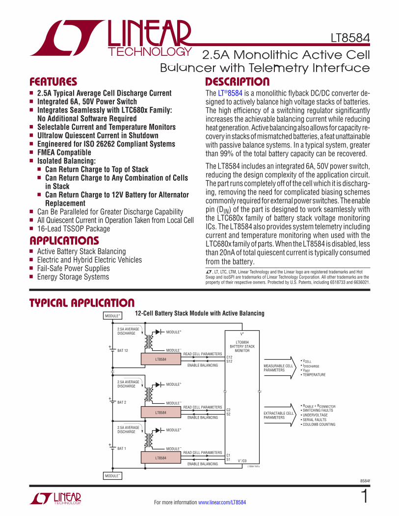
2.5A Monolithic Active Cell Balancer with Telemetry Interface
The LT®8584 is a monolithic flyback DC/DC converter de-signed to actively balance high voltage stacks of batteries. The high efficiency of a switching regulator significantly increases the achievable balancing current while reducing heat generation. Active balancing also allows for capacity re-covery in stacks of mismatched batteries, a feat unattainable with passive balance systems. In a typical system, greater than 99% of the total battery capacity can be recovered.
The LT8584 includes an integrated 6A, 50V power switch, reducing the design complexity of the application circuit. The part runs completely off of the cell which it is discharg-ing, removing the need for complicated biasing schemes commonly required for external power switches. The enable pin (DIN) of the part is designed to work seamlessly with the LTC680x family of battery stack voltage monitoring ICs. The LT8584 also provides system telemetry including current and temperature monitoring when used with the LTC680x family of parts. When the LT8584 is disabled, less than 20nA of total quiescent current is typically consumed from the battery. L, LT, LTC, LTM, Linear Technology and the Linear logo are registered trademarks and Hot Swap and isoSPI are trademarks of Linear Technology Corporation. All other trademarks are the property of their respective owners. Protected by U.S. Patents, including 6518733 and 6636021.
applicaTions
n 2.5A Typical Average Cell Discharge Currentn Integrated 6A, 50V Power Switchn Integrates Seamlessly with LTC680x Family:
No Additional Software Requiredn Selectable Current and Temperature Monitorsn Ultralow Quiescent Current in Shutdownn Engineered for ISO 26262 Compliant Systemsn FMEA Compatiblen Isolated Balancing:
n Can Return Charge to Top of Stackn Can Return Charge to Any Combination of Cells
in Stackn Can Return Charge to 12V Battery for Alternator
Replacementn Can Be Paralleled for Greater Discharge Capabilityn All Quiescent Current in Operation Taken from Local Cell n 16-Lead TSSOP Package
n Active Battery Stack Balancingn Electric and Hybrid Electric Vehiclesn Fail-Safe Power Suppliesn Energy Storage Systems
LT8584
LTC6804BATTERY STACK
MONITOR
MEASURABLE CELLPARAMETERS
2.5A AVERAGEDISCHARGE MODULE+
MODULE+
MODULE–
V+
V–/C0
BAT 12+
MODULE–
READ CELL PARAMETERS
ENABLE BALANCING
•
•
LT8584 TA01a
2.5A AVERAGEDISCHARGE MODULE+
BAT 2+
MODULE–•
•
2.5A AVERAGEDISCHARGE MODULE+
C12S12
LT8584READ CELL PARAMETERS
ENABLE BALANCING
C2S2
LT8584READ CELL PARAMETERS
ENABLE BALANCING
C1S1
BAT 1+
MODULE–•
•
EXTRACTABLE CELLPARAMETERS
• RCABLE + RCONNECTOR• SWITCHING FAULTS• UNDERVOLTAGE• SERIAL FAULTS• COULOMB COUNTING
• VCELL• IDISCHARGE• VREF• TEMPERATURE
12-Cell Battery Stack Module with Active Balancing
LT8584
28584f
For more information www.linear.com/LT8584
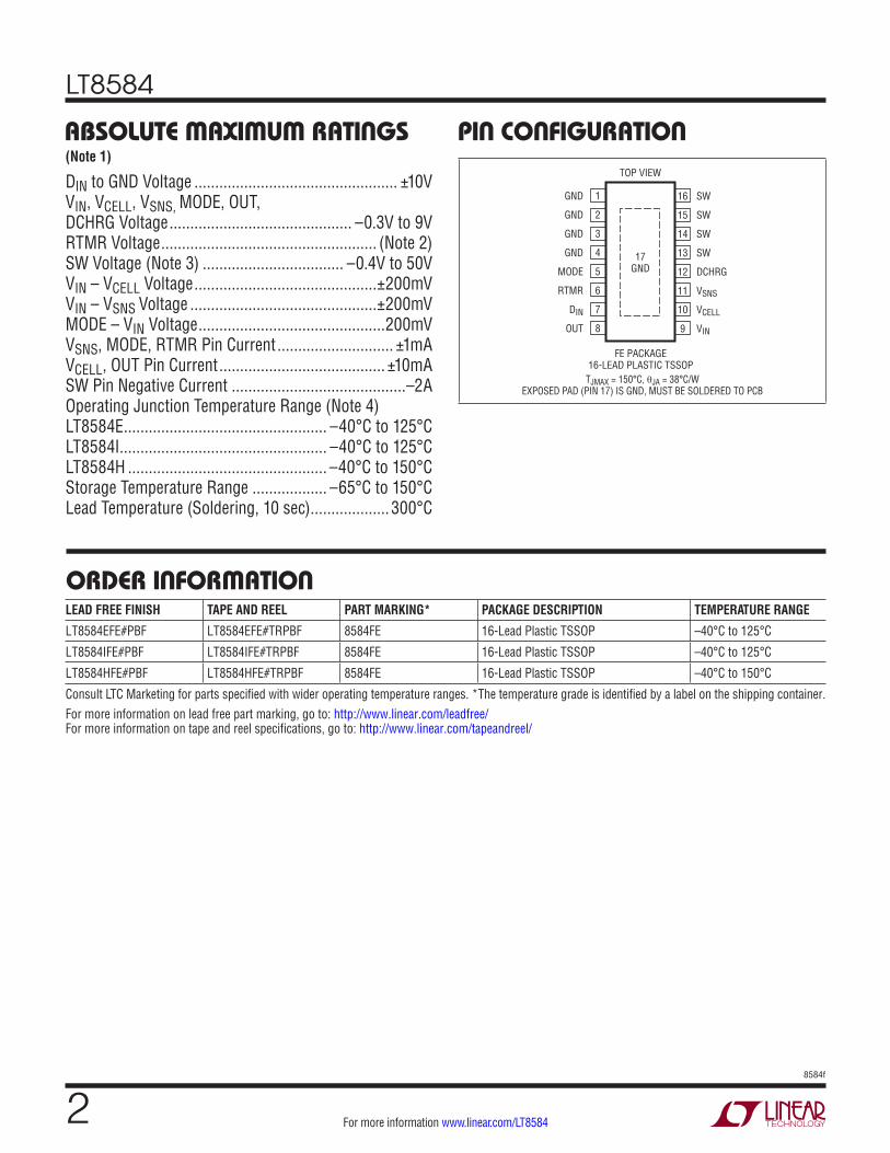
pin conFiguraTionabsoluTe MaxiMuM raTings
DIN to GND Voltage ................................................. ±10VVIN, VCELL, VSNS, MODE, OUT, DCHRG Voltage ............................................ –0.3V to 9VRTMR Voltage .................................................... (Note 2)SW Voltage (Note 3) .................................. –0.4V to 50VVIN – VCELL Voltage ............................................±200mVVIN – VSNS Voltage .............................................±200mVMODE – VIN Voltage .............................................200mVVSNS, MODE, RTMR Pin Current ............................ ±1mA VCELL, OUT Pin Current ........................................ ±10mASW Pin Negative Current ..........................................–2AOperating Junction Temperature Range (Note 4)LT8584E ................................................. –40°C to 125°CLT8584I.................................................. –40°C to 125°CLT8584H ................................................ –40°C to 150°CStorage Temperature Range .................. –65°C to 150°CLead Temperature (Soldering, 10 sec) ................... 300°C
(Note 1)
FE PACKAGE16-LEAD PLASTIC TSSOP
1
2
3
4
5
6
7
8
TOP VIEW
16
15
14
13
12
11
10
9
GND
GND
GND
GND
MODE
RTMR
DIN
OUT
SW
SW
SW
SW
DCHRG
VSNS
VCELL
VIN
17GND
TJMAX = 150°C, θJA = 38°C/W
EXPOSED PAD (PIN 17) IS GND, MUST BE SOLDERED TO PCB
orDer inForMaTionLEAD FREE FINISH TAPE AND REEL PART MARKING* PACKAGE DESCRIPTION TEMPERATURE RANGE
LT8584EFE#PBF LT8584EFE#TRPBF 8584FE 16-Lead Plastic TSSOP –40°C to 125°C
LT8584IFE#PBF LT8584IFE#TRPBF 8584FE 16-Lead Plastic TSSOP –40°C to 125°C
LT8584HFE#PBF LT8584HFE#TRPBF 8584FE 16-Lead Plastic TSSOP –40°C to 150°C
Consult LTC Marketing for parts specified with wider operating temperature ranges. *The temperature grade is identified by a label on the shipping container.For more information on lead free part marking, go to: http://www.linear.com/leadfree/ For more information on tape and reel specifications, go to: http://www.linear.com/tapeandreel/
LT8584
38584f
For more information www.linear.com/LT8584
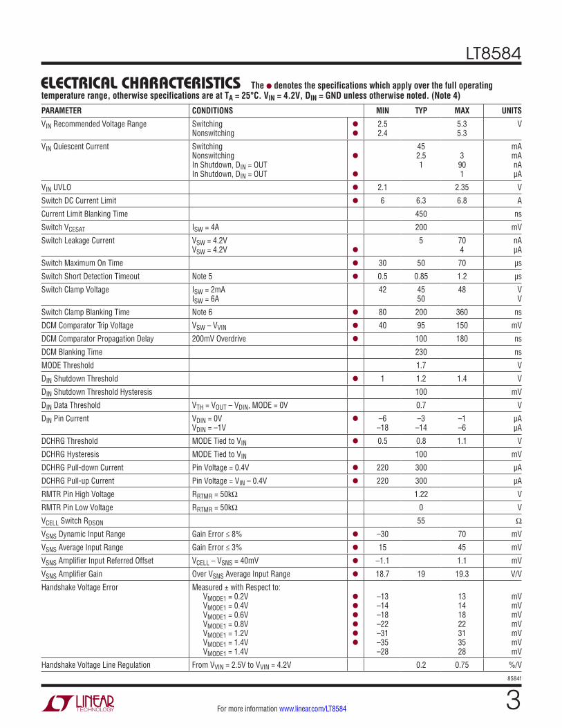
elecTrical characTerisTics The l denotes the specifications which apply over the full operating temperature range, otherwise specifications are at TA = 25°C. VIN = 4.2V, DIN = GND unless otherwise noted. (Note 4)
PARAMETER CONDITIONS MIN TYP MAX UNITS
VIN Recommended Voltage Range Switching Nonswitching
l
l
2.5 2.4
5.3 5.3
V
VIN Quiescent Current Switching Nonswitching In Shutdown, DIN = OUT In Shutdown, DIN = OUT
l
l
45 2.5 1
3
90 1
mA mA nA µA
VIN UVLO l 2.1 2.35 V
Switch DC Current Limit l 6 6.3 6.8 A
Current Limit Blanking Time 450 ns
Switch VCESAT ISW = 4A 200 mV
Switch Leakage Current VSW = 4.2V VSW = 4.2V
l
5 70 4
nA µA
Switch Maximum On Time l 30 50 70 µs
Switch Short Detection Timeout Note 5 l 0.5 0.85 1.2 µs
Switch Clamp Voltage ISW = 2mA ISW = 6A
42 45 50
48 V V
Switch Clamp Blanking Time Note 6 l 80 200 360 ns
DCM Comparator Trip Voltage VSW – VVIN l 40 95 150 mV
DCM Comparator Propagation Delay 200mV Overdrive l 100 180 ns
DCM Blanking Time 230 ns
MODE Threshold 1.7 V
DIN Shutdown Threshold l 1 1.2 1.4 V
DIN Shutdown Threshold Hysteresis 100 mV
DIN Data Threshold VTH = VOUT – VDIN, MODE = 0V 0.7 V
DIN Pin Current VDIN = 0V VDIN = –1V
l –6 –18
–3 –14
–1 –6
µA µA
DCHRG Threshold MODE Tied to VIN l 0.5 0.8 1.1 V
DCHRG Hysteresis MODE Tied to VIN 100 mV
DCHRG Pull-down Current Pin Voltage = 0.4V l 220 300 µA
DCHRG Pull-up Current Pin Voltage = VIN – 0.4V l 220 300 µA
RMTR Pin High Voltage RRTMR = 50kΩ 1.22 V
RMTR Pin Low Voltage RRTMR = 50kΩ 0 V
VCELL Switch RDSON 55 Ω
VSNS Dynamic Input Range Gain Error ≤ 8% l –30 70 mV
VSNS Average Input Range Gain Error ≤ 3% l 15 45 mV
VSNS Amplifier Input Referred Offset VCELL – VSNS = 40mV l –1.1 1.1 mV
VSNS Amplifier Gain Over VSNS Average Input Range l 18.7 19 19.3 V/V
Handshake Voltage Error Measured ± with Respect to: VMODE1 = 0.2V VMODE1 = 0.4V VMODE1 = 0.6V VMODE1 = 0.8V VMODE1 = 1.2V VMODE1 = 1.4V VMODE1 = 1.4V
l
l
l
l
l
l
–13 –14 –18 –22 –31 –35 –28
13 14 18 22 31 35 28
mV mV mV mV mV mV mV
Handshake Voltage Line Regulation From VVIN = 2.5V to VVIN = 4.2V 0.2 0.75 %/V

LT8584
48584f
For more information www.linear.com/LT8584
Note 1: Stresses beyond those listed under Absolute Maximum Ratings may cause permanent damage to the device. Exposure to any Absolute Maximum Rating condition for extended periods may affect device reliability and lifetime.Note 2: Do not apply a positive or negative voltage or current source to RTMR, otherwise permanent damage may occur. Note 3: ABSMAX rating refers to the maximum DC + AC leakage spike. Do not exceed 40VDC on any of the SW pins.Note 4: The LT8584E is guaranteed to meet performance specifications from 0°C to 125°C junction temperature. Specifications over the –40°C to 125°C operating junction temperature range are assured by design, characterization, and correlation with statistical process controls. The LT8584I is guaranteed over the full –40°C to 125°C operating junction temperature range. The LT8584H is guaranteed over the full –40°C to 150°C operating junction temperature range.
Note 5: This is a measure of time duration from the onset of the switch turning on to the time the short-circuit protection circuit is disabled. If the current comparator trips during this duration, the switch error latch is set. This indicates that the connection to the transformer primary is most likely shorted. Note 6: This is a measure of time duration for the switch clamp to operate continuously without setting the switch error latch. If the switch clamp remains engaged longer than the switch clamp blanking time, the switch error latch is set and switching is disabled.Note 7: The voltage proportional to temperature (VTEMP) is measured on the OUT pin while in analog multiplexer MODE 3 or 4. VTEMP must be subtracted from the VCELL voltage that is measured while in analog mux MODE 1. Both measurements should be taken within 100ms of each other to reduce errors in absolute temperature calculation.
SYMBOL PARAMETER CONDITIONS MIN TYP MAX UNITS
tW Decode Window Duration RRTMR = 10kΩ RRTMR = 50kΩ RRTMR = 100kΩ RRTMR = 200kΩ
l
l
l
l
1.76 8
15.6 29.3
1.86 8.4
16.4 31.5
1.96 8.8
17.2 33.7
ms ms ms ms
Decode Window Range l 1.76 33.7 ms
tRST DIN Serial Communication Reset Time l 10 µs
t1 RTMR Start-Up Time RRTMR = 10kΩ l 1.8 5 µs
t2 DIN Hold-Off Time l 50 µs
t3 DIN High Time l 50 µs
t4 DIN Low Time l 50 µs
t5 Discharger Activation Time RRTMR = 10kΩ 900 ns
t6 Discharger Deactivation Time 2.1 µs
SR DIN Slew Rate l 9 V/ms
TiMing characTerisTics The l denotes the specifications which apply over the full operating temperature range, otherwise specifications are at TA = 25°C. MODE = 0V. Refer to Timing Diagram for parameter definition. (Note 4)
The l denotes the specifications which apply over the full operating temperature range, otherwise specifications are at TA = 25°C. VIN = 4.2V, DIN = GND unless otherwise noted. (Note 4)elecTrical characTerisTics
PARAMETER CONDITIONS MIN TYP MAX UNITS
VTEMP Temperature Coefficient (TC) Note 7, °K = (VCELL – VTEMP)/TC 2 mV/°K
VTEMP VTEMP = VIN – VOUT, TJ = 25°C 0.658 V
OUT Pin Clamp Voltage 10mA Sourced from Pin l 1.53 1.6 V
OUT Pin Amplifier Load Regulation IOUT = 10µA to 1mA l 0 0.2 0.4 %/mA
LT8584
58584f
For more information www.linear.com/LT8584
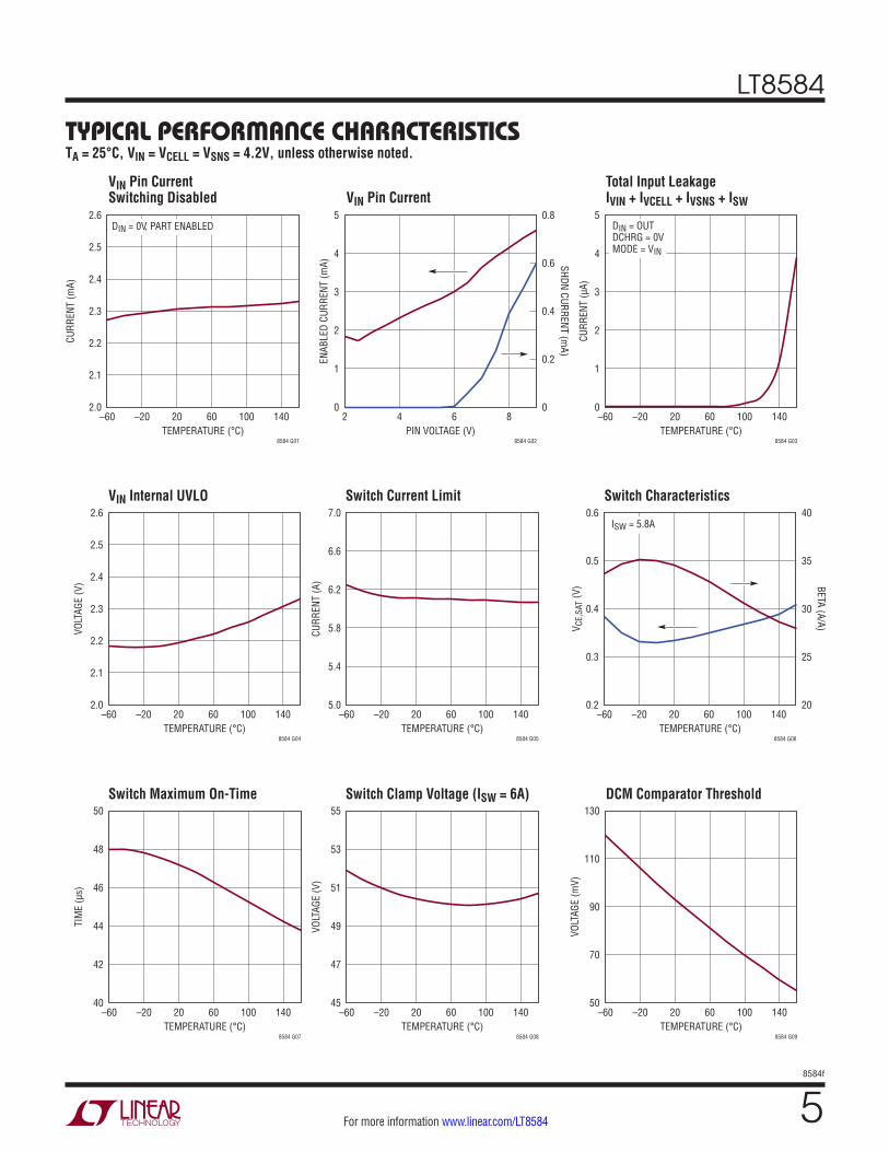
Typical perForMance characTerisTics
VIN Internal UVLO Switch Current Limit Switch Characteristics
Switch Maximum On-Time Switch Clamp Voltage (ISW = 6A) DCM Comparator Threshold
VIN Pin Current Switching Disabled VIN Pin Current
Total Input LeakageIVIN + IVCELL + IVSNS + ISW
TA = 25°C, VIN = VCELL = VSNS = 4.2V, unless otherwise noted.
TEMPERATURE (°C)–60
CURR
ENT
(mA)
2.6
2.5
2.4
2.3
2.2
2.1
2.020
8584 G01
140100–20 60
DIN = 0V, PART ENABLED
PIN VOLTAGE (V)2
ENAB
LED
CURR
ENT
(mA) SHDN CURRENT (m
A)
5
4
3
2
1
0
0.8
0.6
0.4
0.2
06
8584 G02
4 8TEMPERATURE (°C)
–60
CURR
ENT
(µA)
5
4
3
2
1
020
8584 G03
140100–20 60
DIN = OUTDCHRG = 0VMODE = VIN
TEMPERATURE (°C)–60
VOLT
AGE
(V)
2.6
2.5
2.4
2.3
2.2
2.1
2.020
8584 G04
140100–20 60TEMPERATURE (°C)
–60
CURR
ENT
(A)
7.0
6.6
6.2
5.8
5.4
5.020
8584 G05
140100–20 60TEMPERATURE (°C)
–60
V CE,
SAT
(V) BETA (A/A)
0.6
0.5
0.4
0.3
0.2
40
35
30
25
2020 60
8584 G06
–20 140100
ISW = 5.8A
TEMPERATURE (°C)–60
TIM
E (µ
s)
50
48
46
44
42
4020
8584 G07
140100–20 60TEMPERATURE (°C)
–60
VOLT
AGE
(V)
55
53
51
49
47
4520
8584 G08
140100–20 60TEMPERATURE (°C)
–60
VOLT
AGE
(mV)
130
110
90
70
5020
8584 G09
140100–20 60
LT8584
68584f
For more information www.linear.com/LT8584
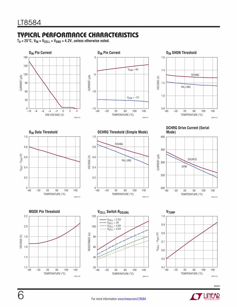
Typical perForMance characTerisTics
DIN Data Threshold DCHRG Threshold (Simple Mode)DCHRG Drive Current (Serial Mode)
DIN Pin Current DIN Pin Current DIN SHDN Threshold
MODE Pin Threshold VCELL Switch RDS(ON) VTEMP
TA = 25°C, VIN = VCELL = VSNS = 4.2V, unless otherwise noted.
DIN VOLTAGE (V)–10
CURR
ENT
(µA)
180
120
150
90
60
30
0–6
8584 G10
0–2–8 –4 42TEMPERATURE (°C)
–60
CURR
ENT
(µA)
0
–5
–10
–1520
8584 G11
140100–20 60
VDIN = 0V
VDIN = –1V
TEMPERATURE (°C)–60
VOLT
AGE
(V)
1.6
1.2
1.4
1.0
0.820
8584 G12
140100–20 60
RISING
FALLING
TEMPERATURE (°C)–60
V OUT
– V
DIN
(V)
1.0
0.6
0.8
0.4
0.2
020
8584 G13
140100–20 60TEMPERATURE (°C)
–60
VOLT
AGE
(V)
1.0
0.6
0.8
0.4
0.2
020
8584 G14
140100–20 60
RISING
FALLING
TEMPERATURE (°C)–60
CURR
ENT
(µA)
400
350
300
250
20020
8584 G15
140100–20 60
SINK
SOURCE
TEMPERATURE (°C)–60
VOLT
AGE
(V)
2.2
1.8
2.0
1.6
1.4
1.220
8584 G16
140100–20 60TEMPERATURE (°C)
–60
RESI
STAN
CE (Ω
)
120
80
100
60
40
2020
8584 G17
140100–20 60
VCELL = 2.5VVCELL = 3VVCELL = 3.6VVCELL = 4.2V
TEMPERATURE (°C)–60
V CEL
L –
V OUT
(V)
1.0
0.7
0.8
0.9
0.6
0.5
0.420
8584 G18
140100–20 60

LT8584
78584f
For more information www.linear.com/LT8584
Typical perForMance characTerisTicsTA = 25°C, VIN = VCELL = VSNS = 4.2V, unless otherwise noted.
Handshake Voltage Error Decode Window Duration Error
OUT Pin Clamp VoltageIOUT = 10mA OUT Pin Amplifier Drive Current
OUT Pin Amplifier1% Settling Time, COUT = 220nF
VSNS Transfer Function VSNS Amplifier GainVSNS AmplifierInput Referred Offset
Handshake Voltage Line Regulation
TEMPERATURE (°C)–60
GAIN
(V/V
)
19.50
19.25
19.00
18.75
18.5020
8584 G20
140100–20 60TEMPERATURE (°C)
–60
OFFS
ET (µ
V)
500
250
0
–250
–50020
8584 G21
140100–20 60
TEMPERATURE (°C)–60
ERRO
R VO
LTAG
E (m
V)
10
5
0
–5
–1020
8584 G22
140100–20 60
SW, ERRFAULTMODE4MODE3MODE2MODE1
TEMPERATURE (°C)–60
REGU
LATI
ON (%
/V)
0.30
0.15
0.10
0.25
0.20
0.05
020
8584 G23
140100–20 60TEMPERATURE (°C)
–60
ERRO
R (%
)
3
2
1
0
–2
–1
–320
8584 G24
140100–20 60
50k
10k
100k
TEMPERATURE (°C)–60
V IN
– V O
UT (V
)
2.0
1.8
1.6
1.4
1.2
1.020
8584 G25
140100–20 60TEMPERATURE (°C)
–60
CURR
ENT
(mA)
10
9
8
7
6
5
4
3
220
8584 G26
140100–20 60
SINK
SOURCE
TEMPERATURE (°C)–60
TIM
E (µ
s)
300
250
200
150
10020
8584 G27
140100–20 60
VCELL – VSNS (mV)0
V CEL
L –
V OUT
(mV)
1200
600
800
1000
400
200
020
8584 G19
60 704010 30 50
LT8584
88584f
For more information www.linear.com/LT8584
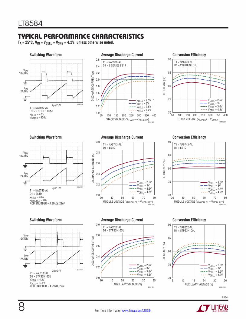
Typical perForMance characTerisTicsTA = 25°C, VIN = VCELL = VSNS = 4.2V, unless otherwise noted.
Average Discharge Current Conversion Efficiency
Switching Waveform Average Discharge Current Conversion Efficiency
Average Discharge Current Conversion Efficiency
Switching Waveform
Switching Waveform
2µs/DIVT1 = NA5920-ALD1 = 2 SERIES ES1JVCELL = 4.2VVSTACK = 400V
VSW10V/DIV
ISW2A/DIV
8584 G28
STACK VOLTAGE (VSTACK+ – VSTACK–)50
DISC
HARG
E CU
RREN
T (A
)
2.6
2.2
2.4
2.0
1.8
1.6
1.4
1.2
1.0150
8584 G29
300250 400350100 200
VCELL = 2.5VVCELL = 3VVCELL = 3.6VVCELL = 4.2V
T1 = NA5920-ALD1 = 2 SERIES ES1J
STACK VOLTAGE (VSTACK+ – VSTACK–)50
EFFI
CIEN
CY (%
)
90
80
85
75
70150
8584 G30
400350100 300250200
VCELL = 2.5VVCELL = 3VVCELL = 3.6VVCELL = 4.2V
T1 = NA5920-ALD1 = 2 SERIES ES1J
2µs/DIVT1 = NA6252-ALD1 = STPS3H100UVCELL = 4.2VVAUX = 13.8VRCD SNUBBER = 4.99kΩ, 22nF
VSW10V/DIV
ISW2A/DIV
8584 G34
AUXILLARY VOLTAGE (V)10
DISC
HARG
E CU
RREN
T (A
)
3.0
2.4
2.6
2.8
2.2
2.0
8584 G35
3525 302015
VCELL = 2.5VVCELL = 3VVCELL = 3.6VVCELL = 4.2V
T1 = NA6252-ALD1 = STPS3H100U
AUXILLARY VOLTAGE (V)6
EFFI
CIEN
CY (%
)
90
80
85
75
70
8584 G36
3624 301812
VCELL = 2.5VVCELL = 3VVCELL = 3.6VVCELL = 4.2V
T1 = NA6252-ALD1 = STPS3H100U
2µs/DIVT1 = NA5743-ALD1 = ES1DVCELL = 3.6VVMODULE = 40VRCD SNUBBER = 4.99kΩ, 22nF
VSW10V/DIV
ISW2A/DIV
8584 G31
MODULE VOLTAGE (VMODULE+ – VMODULE–)30
DISC
HARG
E CU
RREN
T (A
)
3.0
2.4
2.6
2.8
2.2
2.0
8584 G32
8060 705040
VCELL = 2.5VVCELL = 3VVCELL = 3.6VVCELL = 4.2V
T1 = NA5743-ALD1 = ES1D
MODULE VOLTAGE (VMODULE+ – VMODULE–)30
EFFI
CIEN
CY (%
)
90
80
85
75
70
8584 G33
8070605040
T1 = NA5743-ALD1 = ES1D
VCELL = 2.5VVCELL = 3VVCELL = 3.6VVCELL = 4.2V
LT8584
98584f
For more information www.linear.com/LT8584
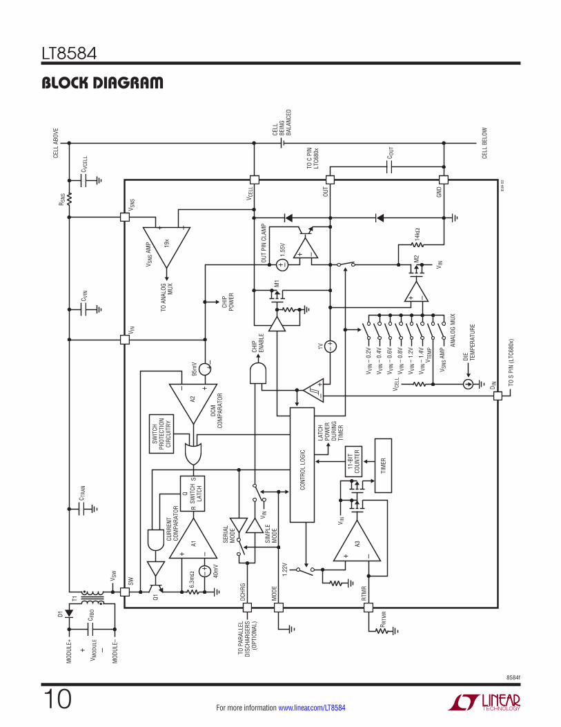
GND (Pin1, Pin 2, Pin 3, Pin 4, Pin 17): Must be soldered directly to local ground plane.
MODE (Pin 5): Serial Enable Pin. Connect this pin to ground to enable serial interface for analog mux control. Connect this pin to VIN to disable the analog mux. When the analog mux is disabled, the OUT pin defaults to VTEMP measurement. Do not float this pin.
RTMR (Pin 6): Serial Interface Timer Pin. Place a resistor from this pin to ground to set the serial count duration window, tW. See the Applications Information section for proper resistor selection.
DIN (Pin 7): Data Input Pin. Take this pin 1V below the OUT pin to initiate switching if MODE pin is connected to VIN, or to select the desired analog mux state if MODE pin is tied to ground. This pin is designed to be directly driven from the LT680x family’s S pins.
OUT (Pin 8): Analog Output Pin. Connect this pin to an accurate voltage monitor to measure a voltage propor-tional to the internal IC temperature, VTEMP, if MODE pin is connected to VIN, or measure the output of the internal analog mux if MODE pin is connected to ground. In analog mux mode, the OUT pin allows voltage monitoring of the VCELL pin, the VSNS pin, or VTEMP. This pin is designed to be directly connected to the LTC680x family’s C pins. Must connect a compensation capacitor to this pin. See the Applications Information section for proper capacitor sizing and placement.
VIN (Pin 9): Supply Pin. Connect this pin directly to the positive battery cell terminal. Must be bypassed with high grade (X5R or better) ceramic capacitor placed close to the transformer’s primary winding connection.
VCELL (Pin 10): Cell Voltage Monitor Pin. This pin provides a Kelvin connection to the battery cell for accurate voltage monitoring. Connect this pin directly to the positive battery cell terminal. The recommended cell voltage is 2.5V to 5.3V.
VSNS (Pin 11): Voltage Sense Pin. Connect this pin to the current sense resistor connected to the primary side of the transformer. Use this pin to measure average current discharged from battery cell (see the Block Diagram). MODE pin must be connected to ground and the internal analog mux must have the VSNS pin selected to use this feature. Input current is determined as (VVCELL – VVSNS)/RSNS.
DCHRG (Pin 12): Discharge Pin. The Discharge pin can be configured as an input or output pin. Connect MODE pin to ground to configure DCHRG as an output pin where DCHRG is driven to VIN during switching and driven to ground when switching is deactivated. The output configuration can be used to drive multiple LT8584’s or other switching regulators in parallel, to boost discharge capability. Connect MODE pin high to configure DCHRG as an input. When configured as an input pin, drive DCHRG pin to VIN to enable switching. Note in this mode that se-rial communication is disabled and the DIN pin must be grounded to initiate switching.
SW (Pin 13, Pin 14, Pin 15, Pin 16): Switch Pin. This is the collector of the internal 6A NPN power switch. Minimize the metal trace area connected to this pin to minimize EMI. Connect the bottom side of the transformer primary to this pin.
pin FuncTions
LT8584
108584f
For more information www.linear.com/LT8584
block DiagraMM
ODUL
E+
+V M
ODUL
E
–M
ODUL
E–
T1 •
•
–+
– +
+–
SWIT
CHLA
TCH
SWIT
CHPR
OTEC
TION
CIRC
UITR
Y
SIM
PLE
MOD
E
SERI
ALM
ODE
CURR
ENT
COM
PARA
TOR
A2A1
6.3m
Ω 40m
V
Q1
QR
S
+ –
DCM
COM
PARA
TOR
95m
V
V SW
SW
C TRA
N
1V
DCHR
GTO
PAR
ALLE
LDI
SCHA
RGER
S(O
PTIO
NAL)
MOD
E
RTM
R
R RTM
R
–+A3
1.22
V
V INV I
N
TIM
ER
11-B
ITCO
UNTE
R
LATC
HPO
WER
DURI
NGTI
MER
CHIP
ENAB
LE
TO A
NALO
GM
UX
V SNS
AM
P
1.55
V
OUT
PIN
CLAM
P
CELL
BEIN
GBA
LANC
ED
TO C
PIN
LTC6
80x
CHIP
POW
ER
CONT
ROL
LOGI
C
+–
+–
+ –
+ –
V VIN
– 0
.2V
V VIN
– 0
.4V
V VIN
– 0
.6V
V VIN
– 0
.8V
V VIN
– 1
.2V
V VIN
– 1
.4V
V CEL
L
V TEM
P
V SNS
AM
P
DIE
TEM
PERA
TURE
TO S
PIN
(LTC
680x
)
ANAL
OG M
UX
V IN
D IN
+ –M
1
OUT
GND
M2
14kΩ
V CEL
L
V IN
C VIN
V SNS
CELL
ABO
VE
CELL
BEL
OW
8584
BD
–+
19x
D1
C FBO
R SNS
C VCE
LL C OUT

LT8584
118584f
For more information www.linear.com/LT8584
Most systems use multiple battery cells connected in series to increase the available capacity and voltage. Individual battery cells must be properly charged where their volt-age and temperature are constantly monitored and never allowed to exceed safe levels; otherwise, the battery’s capacity and life span would be greatly reduced. Linear Technology offers the LTC680x family series of multicell battery stack monitors (BSM) to accomplish this task.
The LT680x monitors each individual cell in the stack and communicates this information through a proprietary serial bus to a central processing unit. If a cell begins to approach the allowable voltage limit, commands are issued to the LT680x to turn on that cell’s passive shunt, bypassing the charging current to that cell and allowing the current to continue to the rest of the cells. The pas-sive shunt current and/or power capability constrains the maximum charging current for the battery stack. Using a passive shunt is also inefficient, and the shunted current produces considerable heat at higher charging currents.
The LT8584 solves the two limitations of passive shunting balancers by actively shunting the charging current and returning the energy back to the battery stack. Instead of the energy being lost as heat, it is reused to charge the rest of the batteries in the stack. The architecture of the LT8584 also solves the problem of reduced run time when one or more of the cells in the stack reaches the lower safety voltage threshold before the entire stack capacity
TiMing DiagraM
operaTionis extracted. Only active balancing can redistribute the charge from the stronger cells (cells with higher voltage) to charge the weaker cells. This allows the weaker cells to continue to supply the load, extracting greater than 96% of entire stack capacity where passive balancing may only extract 80%.
The LT8584 has an integrated 6A switch designed to operate as a boundary mode flyback converter and provides 2.5A average discharge current. The average discharge current is also scalable by using multiple LT8584s to balance each cell. Note that each battery in the stack requires an LT8584 active cell balancer.
The LT8584 flyback topology allows the charge to return between any two points in the battery stack. Most applica-tions use a module approach and return the charge to a local set of 12 series-connected cells monitored by a 12 channel BSM IC, where the output of the flyback converter is designated as VMODULE. The entire battery stack is then constructed using several 12-cell modules connected in series. A second approach is to return the charge to the entire battery stack, where the flyback output is desig-nated as VSTACK. A final option is to return the charge to an auxiliary power rail, designated as VAUX.
The LT8584 has two modes of operation—selectable by the MODE pin—that can be seamlessly integrated with the LT680x or any other battery stack system. In simple
DIN
RTMR
8584 TD
DCHRG
t2 t3tRST t4
t1
t5
t6
tW
SR

LT8584
128584f
For more information www.linear.com/LT8584
operaTionmode, the LT8584 discharger is toggled on/off using a logic input pin. In serial mode, the LT8584 allows the user to measure the discharge current and the die temperature, in addition to the cell voltage.
GENERAL FLYBACK OPERATION
The first cycle will commence approximately 2µs after LT8584 has been commanded to discharge a cell. The LT8584 is configured as a flyback converter operating in boundary mode (the edge of continuous operation), and has three basic states (see Figure 1).
1. Primary-Side Charging
When the switch latch is set, the internal NPN switch turns on, forcing (VVIN – VCESAT) across the primary winding. Consequently, current in the primary coil rises linearly at a rate of (VVIN – VCESAT)/LPRI. The input voltage is mir-rored on the secondary winding as –N • (VVIN – VCESAT) which reverse-biases the secondary-side series diode and prevents current flow in the secondary winding. Thus, energy is stored in the core of the transformer.
2. Secondary-Side Energy Transfer
When current limit is reached, the current limit comparator resets the switch latch and the device enters the second phase of operation, secondary-side energy transfer. The energy stored in the transformer core forward-biases the series diode and current flows into the output capacitor and/or battery. During this time, the output voltage plus the diode drop is reflected back to the primary coil.
3. Discontinuous Mode Detection
During secondary-side energy transfer to the output capacitor, (VMODULE + VDIODE)/N will appear across the primary winding. A transformer with no energy cannot support a DC voltage, so the voltage across the primary winding will decay to zero. In other words, the collector of the internal NPN, SW pins, will ring down from VVIN + (VMODULE + VDIODE)/N to VVIN. When the SW pin voltage falls below VVIN + 95mV, the DCM comparator sets the switch latch and a new switch cycle begins. States 1-3 continue until the part is disabled.
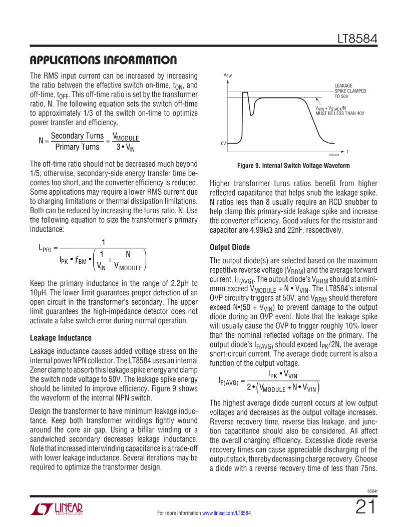
Figure 1. Simplified Discharging Waveforms
8584 F01
IPK
ILPRI
ILSEC
VPRI
VSEC
VVIN +
t
(1)PRIMARY-SIDE
CHARGING
(2)SECONDARY-SIDE
ENERGY TRANSFERAND OUTPUTDETECTION
(3)DISCONTINUOUS
MODEDETECTION
t
t
t
t
VSW
VVIN – VCESATLPRI
VVIN – VCESAT
IPKN
VMODULE – VDIODELSEC
–(VMODULE – VDIODE)N
VMODULE + VDIODE
–N(VVIN – VCESAT)
VMODULE – VDIODEN
VVIN
VCESATVCESAT
LT8584
138584f
For more information www.linear.com/LT8584
operaTionSWITCH PROTECTION
Several protection features are included to reduce the likelihood of permanent damage to the internal power NPN switch: the short-circuit detector, the high-impedance detector, the switch overvoltage protection (OVP), and internal undervoltage lockout (UVLO). These also alert the user when the integrity of the discharge converter has been compromised because of a fault. Switching is disabled during fault conditions.
Short-Circuit Detector
The short-circuit detector detects when the power NPN switch turns off prematurely due to a short in the primary-side winding. If the current comparator trips before the 850ns short detection timeout, the switch error latch will trip. The OUT pin is driven to VVIN – 1.2V, VSW,ERR, during a switch error. The part must be reset to clear the switch error fault.
High-Impedance Detector
The high-impedance detector monitors how long the power NPN switch has been on. If the switch remains on longer than 50µs, the switch maximum on-time, the switch error latch is set and the OUT pin is driven to VVIN – 1.2V, VSW,ERR. The part must be reset to clear the switch error fault.
Overvoltage Protection (OVP)
The OVP circuitry dynamically clamps the NPN collector’s SW pins to 50V. This protects the internal power switch from entering breakdown and causing permanent dam-age. The clamp is also used as a primary-side snubber to absorb the leakage inductance energy. The 200ns switch clamp blanking time determines if the clamp is absorbing a leakage spike or if the switch is turning off while the secondary of the transformer is open. If the switch clamp is on longer than approximately 200ns, the switch error latch is set. The part must be reset to clear the switch error fault.
Internal Undervoltage Lockout (UVLO)
LT8584 protects itself during a UVLO condition by disabling switching. The OUT pin is driven to VVIN – 1.4V, VFAULT, during a UVLO condition. A UVLO fault is non-latching and dominates over a switch fault (Serial Mode requires VIN to remain above 2V for a UVLO fault to be non-latching). Once the UVLO condition is cleared, the OUT pin reverts to normal operation and switching resumes. If the switch fault latch was tripped prior to the UVLO event, the OUT pin will indicate a switch fault, VSW,ERR, only after the UVLO condition is cleared and switching would remain disabled.
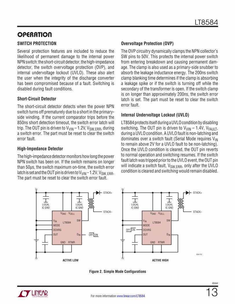
Figure 2. Simple Mode Configurations
LT8584
LOCALIC GND
LOCALIC GND
LOCALIC GND
LOCALIC GND
STACK+
STACK–VSNS VCELL
GND RTMR
SW
DIN
VIN
MODE
DCHRG
OUT
•
•
ACTIVE LOW
8584 F02
ONOFF
LT8584
STACK+
STACK–VSNS VCELL
GND RTMR
SW
DIN
VIN
MODE
DCHRG
OUT
•
•
ACTIVE HIGH
ONOFF
LT8584
148584f
For more information www.linear.com/LT8584
operaTionSIMPLE MODE OPERATION
Connecting the MODE pin to the VIN pin configures the LT8584 as a simple discharger with a simple on/off shutdown pin. Two shutdown options are provided to handle either an active high (DCHRG) or an active low input (DIN), see Figure 2. Connect DIN to ground and use DCHRG pin for an active high input, or connect DCHRG to VIN and use DIN as an active low input. The part will begin switching once the DIN pin is low and DCHRG is high. Figure 3 shows the enable logic function. Never drive DIN more than 0.4V below the local ground while operating in active-high simple mode.
OUT Pin in Simple Mode
The OUT pin defaults to VTEMP, a voltage proportional to the die temperature, and is measured with respect to the cell voltage such that VTEMP = VVCELL – VOUT. This can be used to monitor the internal die temperature for system diagnostics. The OUT pin will also output two distinct in-dication voltage levels, VVIN – 1.4V, VFAULT, for an internal UVLO condition, or VVIN – 1.2V, VSW,ERR, for a switch error. VTEMP is not allowed to exceed 1V (equivalent to 180°C)1. This makes both the fault and switch error volt-ages deterministic. The switch error latch is set when the power NPN switch has encountered a fault (see the Switch Protection section for more details).
Figure 4. Serial Communication Decode
Figure 3. Simple Mode Enable Logic8584 F03
ENABLEBALANCING
DCHRGDIN
8584 F04
SHUTDOWN SHUTDOWNSERIAL DECODE ENABLED WITHCORRECT STATE
DECODE WINDOW
16.3msRRTMR = 100kΩ
VCELLSELECTED
VCELL SELECTEDVOLTAGE MODEHANDSHAKE
ANALOG MUX ACTIVATED TO DESIRED INPUT
OUT WILL NEVER BE DRIVEN BELOW VVIN – 1.435VOUT PIN CLAMP IS ACTIVE BELOW VVIN – 1.53V
DIN
t
t
t
RTMR
1.22V
OUT
VVIN
VVIN
VVIN – 1.4V
VVIN – 0.2VVVIN – 0.4V
VVIN – 0.6VVVIN – 0.8V
1 Not verified during production testing.
LT8584
158584f
For more information www.linear.com/LT8584
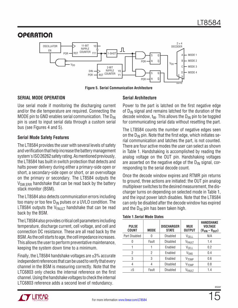
operaTion
SERIAL MODE OPERATION
Use serial mode if monitoring the discharging current and/or the die temperature are required. Connecting the MODE pin to GND enables serial communication. The DIN pin is used to input serial data through a custom serial bus (see Figures 4 and 5).
Serial Mode Safety Features
The LT8584 provides the user with several levels of safety and verification that help increase the battery management system's ISO 26262 safety rating. As mentioned previously, the LT8584 has built in switch protection that detects and halts power delivery during either a primary-side open or short, a secondary-side open or short, or an overvoltage on the primary or secondary. The LT8584 outputs the VSW,ERR handshake that can be read back by the battery stack monitor (BSM).
The LT8584 also detects communication errors including too many or too few DIN pulses or a UVLO condition. The LT8584 outputs the VFAULT handshake that can be read back by the BSM.
The LT8584 also provides critical cell parameters including temperature, discharge current, cell voltage, and cell and connection DC resistance. These are all read back by the BSM. As the cell starts to age, the cell impedance increases. This allows the user to perform preventative maintenance, keeping the system down time to a minimum.
Finally, the LT8584 handshake voltages are ±3% accurate independent references that can be used to verify that every channel in the BSM is measuring correctly. Note that the LTC6803 only checks the internal reference on the first channel. Using the handshake voltages to check the internal LTC6803 reference adds a second level of redundancy.
Serial Architecture
Power to the part is latched on the first negative edge of DIN signal and remains latched for the duration of the decode window, tW. This allows the DIN pin to be toggled for communicating serial data without resetting the part.
The LT8584 counts the number of negative edges seen on the DIN pin. Note that the first edge, which initiates se-rial communication and latches the part, is not counted. There are four active modes the user can select as shown in Table 1. Handshaking is accomplished by reading the analog voltage on the OUT pin. Handshaking voltages are asserted on the negative edge of the DIN signal, cor-responding to the serial decode count.
Once the decode window expires and RTMR pin returns to ground, three actions are initiated: the OUT pin analog multiplexer switches to the desired measurement, the dis-charger turns on depending on selected mode in Table 1, and the input power latch disables. Note that the LT8584 can only be disabled after the decode window has expired and the DIN pin has been taken high.
Table 1.Serial Mode States
PULSE COUNT MODE
DISCHARGER STATE
MUX OUTPUT
HANDSHAKE VOLTAGE
(VVIN – VOUT)
Part Disabled 0 Disabled VCELL N/A
0 Fault Disabled VFAULT 1.4
1 1 Enabled VCELL 0.2
2 2 Enabled VSNS 0.4
3 3 Enabled VTEMP 0.6
4 4 Disabled VTEMP 0.8
≥5 Fault Disabled VFAULT 1.4
Figure 5. Serial Communication Architecture8584 F05
2-BITRIPPLE
COUNTERY0Y1
POR
RST
Q
Q
S
R
MODE 1
MODE 2
MODE 3
MODE 4
POR
Q
Q
S
R
1-SHOT
11-BITRIPPLE
COUNTER
OSCILLATOR
ENPOR
VDD
PORDIN
Y0
Y11RST
VDD
A
B
C
D
2 × 4DECODER
a b
LT8584
168584f
For more information www.linear.com/LT8584
operaTionSerial Timer Decode Window
The timer initiates on the first negative edge on the DIN pin. RTMR pin remains high for the duration of the timer which signifies the decode window for the serial input counter. A resistor from the RTMR pin to ground sets the decode window duration. The duration can be accurately set from 1.9ms (RRTMR = 10k) to 31ms (RRTMR = 200k). The timer can be set outside this range, but the accuracy decreases. The serial input counter stops counting and latches the data once the RTMR pin goes low; after which, the OUT pin amplifier input MUX selects the desired measurement, and the discharger is set to the right state.
Serial Communication Fault Modes
The serial interface has several fault monitors that prevent entering undesired modes due to a communication error. The OUT pin is set to VVIN – 1.4V to indicate the LT8584 is in fault. The part remains in fault from the onset of RTMR going high until the first count is detected. If no count is seen by the serial input counter during the decode window, the fault is latched. If the serial input counter counts higher than 4 negative edges, the fault latch is set.
A third latching fault occurs if an internal undervoltage lockout (UVLO) is detected during the decode window. This protects against undesired operation if data latches or the serial input counter were reset. The part must be reset by taking DIN high to clear a fault.
DIN Pin and Serial Bus Timing
Several internal passive filters are added to the data bus to prevent injected system noise corrupting serial com-munication. These filters have time constants that place constraints on the serial communication timing require-ments (see the Timing Diagram). The LT8584 can reject up to 4µs of erroneous glitches on the DIN pin in either direction. The power latch filter can also reject up to a 4µs glitch on DIN.
The DIN pin has built-in hysteresis of approximately 100mV. This allows the serial input counter to recognize both slow and fast edges without erroneous behavior. The discharger activation or deactivation time is typically less than 3µs and is a direct indication of the switch enable latch state.
OUT Pin Analog MUX
An internal multiplexer, MUX, selects between VCELL and the OUT pin amplifier based on one of the selected Serial Modes shown in Table 1. The OUT pin amplifier has a 5kΩ internal load and has several inputs including: VTEMP, the 19•VSNS amplifier, and six handshake voltages. The internal MUX defaults to VCELL in shutdown—consuming no power in the process—and provides a 55Ω nominal resistance from the VCELL pin to the OUT pin. Figure 6 shows the connection of the OUT pin to a BSM and its internal analog MUX.
The MUX switches over to one of the handshake voltage levels once both the LT8584 and the decode window are activated. The OUT amplifier will indicate a fault at start-up until the serial input counter recognizes the first negative edge on DIN. Subsequent negative edges on DIN cause the MUX to select the handshake voltage corresponding to the number of edges counted. These voltage levels provide a means of verifying if the serial interface has recognized the correct count. Note that the OUT pin amplifier has an approximate 200µs one percent settling time when driving a 220nF load capacitance.
Once the RTMR pin goes low, the MUX selects the OUT pin mode corresponding to the number of serial input counts (see Table 1 for available modes). The part can also be placed in shutdown when RTMR is low and the decode window has expired.
VCELL Measurement
The user can measure the cell voltage by measuring the voltage on the OUT pin either with the part disabled (discharger off) or with the part enabled in MODE 1 (dis-charger on), see Table 1. The LT8584 uses an internal PMOS switch with RDSON = 55Ω to connect VCELL to the OUT pin. Note that any current flowing into or out of the OUT pin will cause a measurement error due to the IR drop across the switch.
VSNS 19× Amplifier
An amplifier is provided to allow the user to monitor the discharger current. This measurement can only be per-formed when the discharger is on (MODE 2). The differ-ential voltage between VVCELL and VVSNS is amplified 19×.

LT8584
178584f
For more information www.linear.com/LT8584
operaTion
8584 F06
LT8584
CONTROL
VCELL VSNS
RSNS
VIN SW
ANALOG MUX
VCELL
VTEMP
VSNS AMP
VIN – 0.2V
VIN – 0.4V
VIN – 0.6V
VIN – 0.8V
VIN – 1.2V
VIN – 1.4V
COUNTER
OUT C2
DINGND
MODE
RTMR
DCHRG
1:4
•
• +
–VMODULE
LT8584
CONTROL
VCELL VSNS
RSNS
VIN SW
ANALOG MUX
VCELL
VTEMP
VSNS AMP
VIN – 0.2V
VIN – 0.4V
VIN – 0.6V
VIN – 0.8V
VIN – 1.2V
VIN – 1.4V
COUNTER
OUT
DINGND
MODE
RTMR
DCHRG
1:4
•
• +
–VMODULE
BAT2+
+BAT1
S2
C1
C0
S1 DCC1BIT
DCC2BIT
ADC
LTC680x
Figure 6. Serial Mode Analog MUX Connection
LT8584
188584f
For more information www.linear.com/LT8584
operaTionThis reduces errors due to input offset in the measure-ment circuitry connected to the OUT pin. It also allows the use of low-value resistors, and thus, yields greater overall efficiency.
For accuracy, the VIN pin should be tied to the VSNS pin to include both the LT8584 bias current and the internal NPN base drive current. Tying the VIN pin to the VSNS pin changes the overall gain to 20x. Tying the VIN pin to the VCELL measures transformer current only and the overall gain remains 19x.
The VSNS amplifier has a –30mV to 70mV dynamic input range. Internal filtering and circuit architecture allows ac-curate measurements even when the input current contains negative components. The VSNS amplifier requires that the average input current remain positive. VVIN – VOUT is not allowed to exceed 1V during VSNS measurement to guarantee that both VFAULT and VSW,ERR are deterministic. This sets the maximum average input range, VVCELL – VVSNS, to 50mV.
Die Temperature Output
The user can also monitor the die temperature by se-lecting either MODE 3 (discharger enabled) or MODE 4 (discharger disabled). The voltage VVCELL – VOUT, VTEMP, is proportional to the absolute temperature in degrees Kelvin. Thus, the user needs to take two measurements to calculate the die temperature. Temperature data gives the user a second means to verify if the discharger is on as well as to monitor environmental conditions. VTEMP is not allowed to exceed 1V (equivalent to 180°C)1 to make both VFAULT and VSW,ERR deterministic.
The following equation is used to determine the internal die temperature in degrees Celsius:
TJ(°C) =
VTEMP − 0.6090.00197
where VTEMP = VVCELL – VOUT and expressed in volts. Although the absolute die temperature can deviate from the above equation by ±25°C, the relationship between VTEMP and the change in die temperature is well defined. The offset error can be calibrated out using an accurate system temperature monitor like that in the LTC680x family of parts. There is also a small VVCELL dependence on VTEMP which can be corrected using the following expression:
TJ,CORR (°C) = TJ,CAL + (4.2V – VCELL) • 2°C
where TJ,CORR is the corrected die temperature and TJ,CAL is die temperature calculated from the previous equation.
Serial Mode Differential Measurements
All parameters including handshake voltages, VSNS, and VTEMP are extracted differentially by taking two sequential measurements and doing a subtraction. Figure 7 shows the method for extracting a given parameter, VPAR, from the highlighted LT8584. The LT8584 directly below the LT8584 under measurement must be forced to select VCELL (MODE 0) and becomes the negative reference for both sequential measurements.
Table 2. MODE Selection During Differential MeasurementsSERIAL MODE STATE
DESIRED PARAMETER 1ST MEASUREMENT 2ND MEASUREMENT
Handshake Voltage MODE 0During Decode
WindowVSNS MODE 1 MODE 2VTEMP, Balancer Enabled MODE 1 MODE 3VTEMP, Balancer Disabled MODE 0 MODE 4
Selecting VCELL for the first measurement is performed by entering either MODE 0 (balancer disabled) or MODE 1 (balancer enabled). Use Table 2 to determine which VCELL to reference for a given parameter. All measurements are taken after the decode window has expired, unless otherwise noted.
VPAR = 1st Measurement – (2nd Measurement) = VCELL – (VCELL – VPAR)
The LTC6803’s channel above the channel under measure-ment will have a voltage higher than a standard cell, VCELL + VPAR, see Figure 7. The LT8584 was architected to protect the LTC6803’s ADC inputs and to guarantee that they well never be stressed beyond their absolute maximum rating.
DCHRG Output
The DCHRG pin allows the LT8584 to operate several dis-chargers in parallel. The DCHRG pin goes high when the switch enable latch is set. The DCHRG pin can be used to directly drive the DCHRG pin of another LT8584 configured in simple mode (MODE pin connected to VIN) or to directly drive the shutdown pin of another power converter. It has the ability to sink or source currents up to 300µA. 1 Not verified during production testing.

LT8584
198584f
For more information www.linear.com/LT8584
operaTion
Figu
re 7
. Ser
ial M
ode
Diffe
rent
ial M
easu
rem
ents
8584
F07
BAT4
V CEL
L4+ –LT
8584
• • •
• • •
• • •
• • •
• • •
• • •
• • •
OUT
V CEL
L
GND
BAT3
V CEL
L3+ –LT
8584
ANAL
OG M
UXSE
LECT
ING
V CEL
L
OUT
V CEL
L
GND
BAT2
V CEL
L2+ –
V CEL
L4+ –
V CEL
L3+ –
V CEL
L2+ –
LT85
84OU
T
V CEL
L
GND
BAT1
LT85
84OU
T
V CEL
L
GND
ANAL
OG M
UXSE
LECT
ING
V CEL
L
ADC
LTC6
80x
C3C4 C2 C1 C0
BAT4
V CEL
L4+ –LT
8584
• • •
• • •
• • •
• • •
• • •
• • •
• • •
OUT
V CEL
L
GND
BAT3
V CEL
L3+ –LT
8584
ANAL
OG M
UXSE
LECT
ING
PARA
MET
ER
OUT
V CEL
L
GND
BAT2
V CEL
L2+ –
V CEL
L4 +
V P
AR,3
V CEL
L3 –
V PAR
,3
+ – + –
V CEL
L2+ –
LT85
84OU
T
V CEL
L
GND
BAT1
LT85
84OU
T
V CEL
L
GND
ANAL
OG M
UXSE
LECT
ING
V CEL
L
ADC
LTC6
80x
C3C4 C2 C1 C0
MEA
SURE
MEN
T 1
(VCE
LL)
MEA
SURE
MEN
T 2
(VCE
LL –
VPA
R)
LT8584
208584f
For more information www.linear.com/LT8584
applicaTions inForMaTionThe LT8584 can be used as a discharger for balancing the charge in battery or supercapacitor stack systems. The user can choose either simple mode or serial mode. Most applications will use the LTC680x to drive the LT8584; however, the LT8584 can be driven from any battery stack monitor. Simple mode can be employed using either active high or active low logic, increasing its interface flexibility.
COMPONENT SELECTION
Few external components are required to achieve balanc-ing. The only external components are the transformer, the output diode(s), the VIN bypass capacitors, the RSNS resistor (for measuring discharge current), the RRTMR resis-tor (for serial mode), and in some cases, a RCD snubber.
The equations are shown for a module based approach described in the Operation section. VMODULE becomes VSTACK in all equations for applications returning charge to the entire stack voltage, and VMODULE becomes VAUX for all applications returning charge to an auxiliary power rail.
Transformer Design
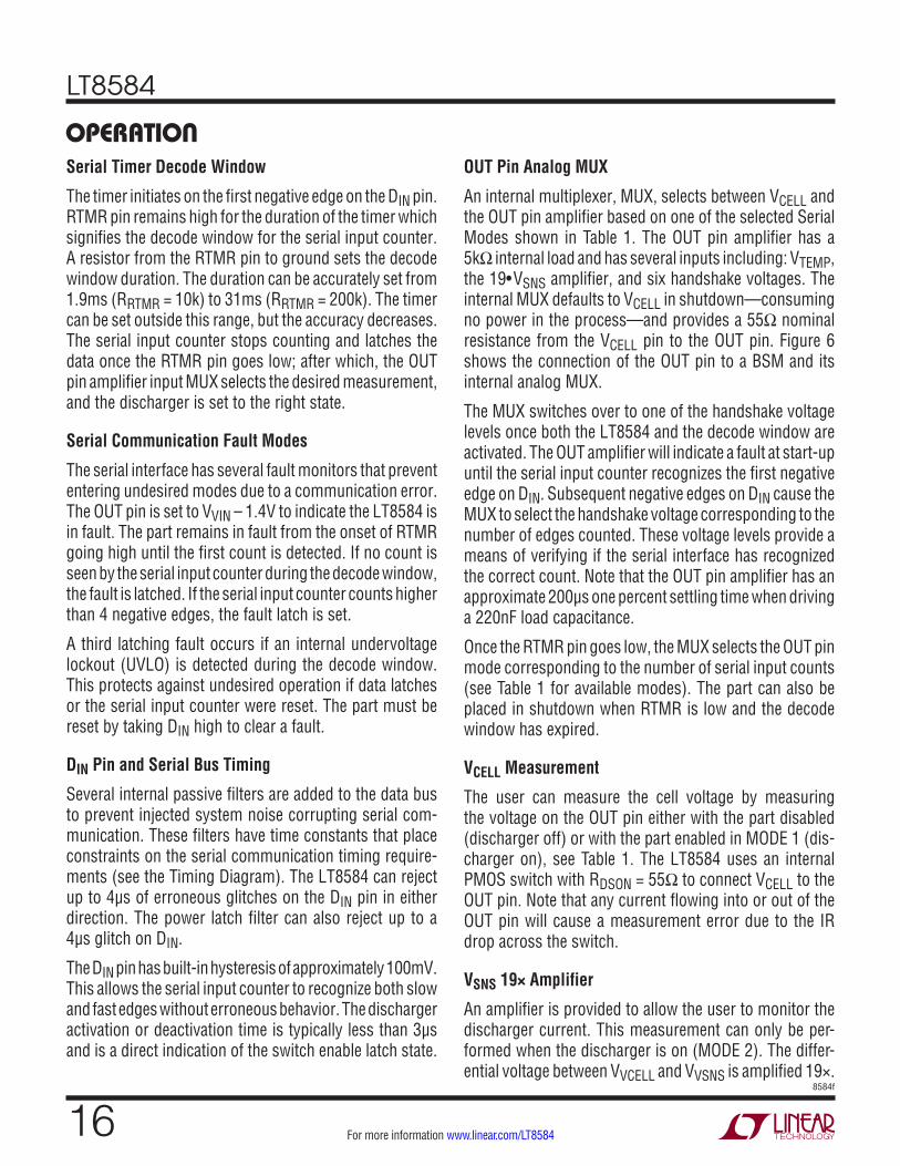
The transformer design should yield overall converter efficiencies greater than 80%. This reduces heat dissipa-tion and allows for a smaller converter PCB footprint. A proper transformer design balances core losses with winding losses. The LT8584 converter operates in DCM where the flux swing in the transformer is the greatest. This shifts most of the heat loss from winding loss to core loss. Reduce transformer core flux swing by lowering the air-gap permeability. A lower permeability requires more Figure 8. Effect of Secondary Winding Capacitance
turns to achieve a desired primary inductance; thus, a bal-ance can be achieved between core and winding losses. Recommended transformers are given in Table 3 that have been optimized for efficiency and size. Use the following guidelines when designing new transformers.
Reduce the transformer size by designing the boundary-mode operating frequency between 100kHz and 150kHz. The peak primary current is fixed at 6A by the chip. The transformer turns ratio, N, should be selected by optimiz-ing the converter input RMS current, i.e. battery discharge current. The RMS input current can be estimated as:
IRMS,IN = IPK •
ƒBM • tON
3
Note that negative switch current reduces the RMS input current by effectively reducing the boundary-mode fre-quency, ƒBM, (see Figure 8). Reduce the overall reflected capacitance on the SW node by reducing the output diode and transformer interwinding parasitic capacitances.
Table 3. Recommended Transformers
MANUFACTURER PART NUMBERRECOMMENDED
OUTPUT RANGE (V)RCD SNUBBER
REQUIRED SIZE W × L × H (mm) LPRI (µH) TURNS RATIO (PRI:SEC)
Coilcraft www.coilcraft.com
NA6252-AL NA5743-AL NA5920-AL*
10 to 35 30 to 80
100 to 400
Yes Yes No
15.24 × 12.7 × 11.43 15.24 × 12.7 × 11.43 15.24 × 12.7 × 11.43
4 4 4
11:15 1:4
1:24
Cooper Bussmann www.cooperindustries.com
CTX02-19175-R CTX02-19174-R CTX02-19176-R*
10 to 35 30 to 80
100 to 400
Yes Yes No
15 × 13 × 12 15 × 13 × 12 15 × 13 × 12
4 4 4
3:4 1:4
1:24
Würth www.we-online.com
750314019_R01 750314018_R02 750314020_R03*
10 to 35 30 to 80
100 to 400
Yes Yes No
15.24 × 13.34 × 11.43 15.24 × 13.34 × 11.43 15.24 × 13.34 × 11.43
4 4 4
3:4 1:4
1:24
* Switch error latch may trip when starting at voltages lower than the recommended output range.
8584 F08t
VSW
ISEC
IPRI
NO SEC.CAPACITANCE
SEC. DISCHARGE
LT8584
218584f
For more information www.linear.com/LT8584
applicaTions inForMaTion
Figure 9. Internal Switch Voltage Waveform
The RMS input current can be increased by increasing the ratio between the effective switch on-time, tON, and off-time, tOFF. This off-time ratio is set by the transformer ratio, N. The following equation sets the switch off-time to approximately 1/3 of the switch on-time to optimize power transfer and efficiency.
N =
Secondary TurnsPrimary Turns
=VMODULE3 • VIN
The off-time ratio should not be decreased much beyond 1/5; otherwise, secondary-side energy transfer time be-comes too short, and the converter efficiency is reduced.Some applications may require a lower RMS current due to charging limitations or thermal dissipation limitations. Both can be reduced by increasing the turns ratio, N. Use the following equation to size the transformer’s primary inductance:
LPRI =1
IPK • ƒBM • 1VIN
+N
VMODULE
⎛
⎝⎜
⎞
⎠⎟
Keep the primary inductance in the range of 2.2µH to 10µH. The lower limit guarantees proper detection of an open circuit in the transformer’s secondary. The upper limit guarantees the high-impedance detector does not activate a false switch error during normal operation.
Leakage Inductance
Leakage inductance causes added voltage stress on the internal power NPN collector. The LT8584 uses an internal Zener clamp to absorb this leakage spike energy and clamp the switch node voltage to 50V. The leakage spike energy should be limited to improve efficiency. Figure 9 shows the waveform of the internal NPN switch.
Design the transformer to have minimum leakage induc-tance. Keep both transformer windings tightly wound around the core air gap. Using a bifilar winding or a sandwiched secondary decreases leakage inductance. Note that increased interwinding capacitance is a trade-off with lower leakage inductance. Several iterations may be required to optimize the transformer design.
Higher transformer turns ratios benefit from higher reflected capacitance that helps snub the leakage spike. N ratios less than 8 usually require an RCD snubber to help clamp this primary-side leakage spike and increase the converter efficiency. Good values for the resistor and capacitor are 4.99kΩ and 22nF, respectively.
Output Diode
The output diode(s) are selected based on the maximum repetitive reverse voltage (VRRM) and the average forward current, IF(AVG). The output diode’s VRRM should at a mini-mum exceed VMODULE + N • VVIN. The LT8584’s internal OVP circuitry triggers at 50V, and VRRM should therefore exceed N•(50 + VVIN) to prevent damage to the output diode during an OVP event. Note that the leakage spike will usually cause the OVP to trigger roughly 10% lower than the nominal reflected voltage on the primary. The output diode’s IF(AVG) should exceed IPK/2N, the average short-circuit current. The average diode current is also a function of the output voltage.
IF(AVG) =IPK • VVIN
2 • VMODULE +N • VVIN( )The highest average diode current occurs at low output voltages and decreases as the output voltage increases. Reverse recovery time, reverse bias leakage, and junc-tion capacitance should also be considered. All affect the overall charging efficiency. Excessive diode reverse recovery times can cause appreciable discharging of the output stack, thereby decreasing charge recovery. Choose a diode with a reverse recovery time of less than 75ns.
8584 F06t
VSW
0V
VVIN + VSTACK/NMUST BE LESS THAN 40V
LEAKAGESPIKE CLAMPEDTO 50V
LT8584
228584f
For more information www.linear.com/LT8584
applicaTions inForMaTionDiode leakage current under high reverse bias bleeds the output battery/capacitor stack of charge. Choose a diode that has minimal reverse bias leakage current. Diode junction capacitance is reflected back to the primary, and energy is lost during negative NPN collection conduction. Choose a diode with minimal junction capacitance. Table 4 recommends several output diodes for various output voltages that have adequate reverse recovery times.
Flyback Output Capacitor
Every balancer flyback output must have a ceramic capaci-tor on its output. The output capacitor serves as a local, low impedance return path. It also aids during a connection failure, adding charge storage to allow the OVP circuit to detect an open. The capacitor should be sized to allow roughly 10 switch cycles when charging the output from ground to the nominal output voltage, VOUTPUT,NOM. Use the following equation to size the output capacitor:
CFBO ≥400 •LPRIMARY
V2OUTPUT,NOM
The voltage surge rating must exceed 50•N. The volt-age surge rating is usually specified as a multiple of the maximum operating voltage. For capacitor maximum operating voltages less than 100V, the surge rating is
2.5x. For operating voltage between 100V and 630V, the surge rating is typically 1.5x; and for voltages higher than 1000V, the surge rating is 1.2x.
Bypass Capacitors
The LT8584 should be bypassed using 3 capacitors, CVIN, CVCELL, and CTRAN (see Block Diagram), using a high-grade (X5R or better) ceramic capacitors. CVIN should be placed close to the VIN pin and should be sized between 1μF and 4.7μF. CTRAN must be placed close to the transformer’s primary winding connection and the IC local ground. The capacitance should range between 47μF and 100μF. Simple mode should have VSNS, VCELL, and DCHRG shorted to VIN, which provides an excellent landing for both the transformer primary and a single bypass cap (see the Recommended Layout section). CVIN may be omitted in Simple Mode provided that the CTRAN capacitor is in close proximity to the VIN pin. CVCELL is used for bulk capacitance and should be place close to the battery input connection. Ceramic capacitors are a good choice for bypassing due to their moderate density, low internal series impedance, and very low leakage current. Note that capacitor leak-age current at a given operating voltage goes down with increasing capacitor voltage rating. Ceramic capacitors offer the lowest leakage current, while most electrolytic capacitors are quite leaky.
Table 4. Recommended Output Diodes
MANUFACTURERRECOMMENDED TRANSFORMER
TURNS RATIO (N) RANGE PART NUMBER IF(AVG) (A)VRRM (V) trr (ns)
JUNCTION CAPACITANCE (pF) PACKAGE
STMicroelectronics 1 to 2 STPS3H100U 3 100 N/A 90 SMB
STPS2H100AY* 2 100 N/A 50 SMA
2 to 4 STTH102AY* 1 200 20 12 SMA
10 to 24 STTH112A 1 1200 75 SMA
Fairchild Semiconductor www.fairchildsemi.com
1 to 2 ES2B 2 100 20 18 SMB
2 to 4 ES1D 1 200 15 7 SMA
4 to 8 ES1G 1 400 35 10 SMA
6 to 12 ES1J 1 600 35 8 SMA
Vishay www.vishay.com
1 to 2 SS2H10* 2 100 N/A 70 SMB
U2B 2 100 20 16 SMB
2 to 4 ES1D 1 200 15 10 SMA
ES07D-M* 1.2 200 25 5 SMF
10 to 20 US1M 1 1000 50 10 SMA
*AEC-Q101 Qualified
LT8584
238584f
For more information www.linear.com/LT8584
applicaTions inForMaTionDischarge Current Sense Resistor
The discharge current sense resistor, RSNS, should only be used in serial mode. Omit this resistor and short VSNS and VCELL to VIN in simple mode. The maximum sense voltage between VVSNS and VVCELL is 50mV. It is recom-mended to design for a nominal sense voltage of 30mV. It is not recommended to design for a nominal sense voltage below 20mV since the input offset voltage of the differential amplifier contributes more error at the lower range.
RSNS =
VCELL − VSNSIDIS,AV
=30mV2.5A
= 12mΩ
The internal amplifier amplifies the voltage difference between VVSNS and VVCELL 20× when VIN is tied to VSNS. The voltage is referenced from VCELL such that:
VVCELL – VOUT = 20 • (RSNS • IDIS,AV)
The measurement is the average discharge current, IDIS,AV, and not the RMS value. The output, VVIN – VOUT, is clamped to a maximum of 1V.
Decode Window Resistor, RRTMR
RTMR pin is used to set the duration of the decode window and is programmed by selecting the value of the resis-tor connected between RTMR and GND. This pin is used in serial mode only. Ground this pin when using simple mode. The decode window is programmable from 1.9ms to 31ms. Set the decode window duration 30% longer than the required time to set the LT8584 in MODE 4 and read back the handshake voltage. This allows the system to detect if there is a communication error. Set RRTMR based on following equation:
RRTMR (kΩ) = 0.015 • t2W + 5.9 • tW – 1.1
where RRTMR is given in kΩ and tW is given in ms.
The RTMR pin is driven to 1.22V approximately 2µs after the part is first enabled. This indicates the decode window is active. The RTMR pin is taken low after the decode window expires. The internal decoder states are latched on the falling edge of RTMR (see Figure 4). The OUT pin multiplexer then selects the correct input corresponding to the programmed mode (refer to Table 1).
OUT Pin Compensation and Filtering
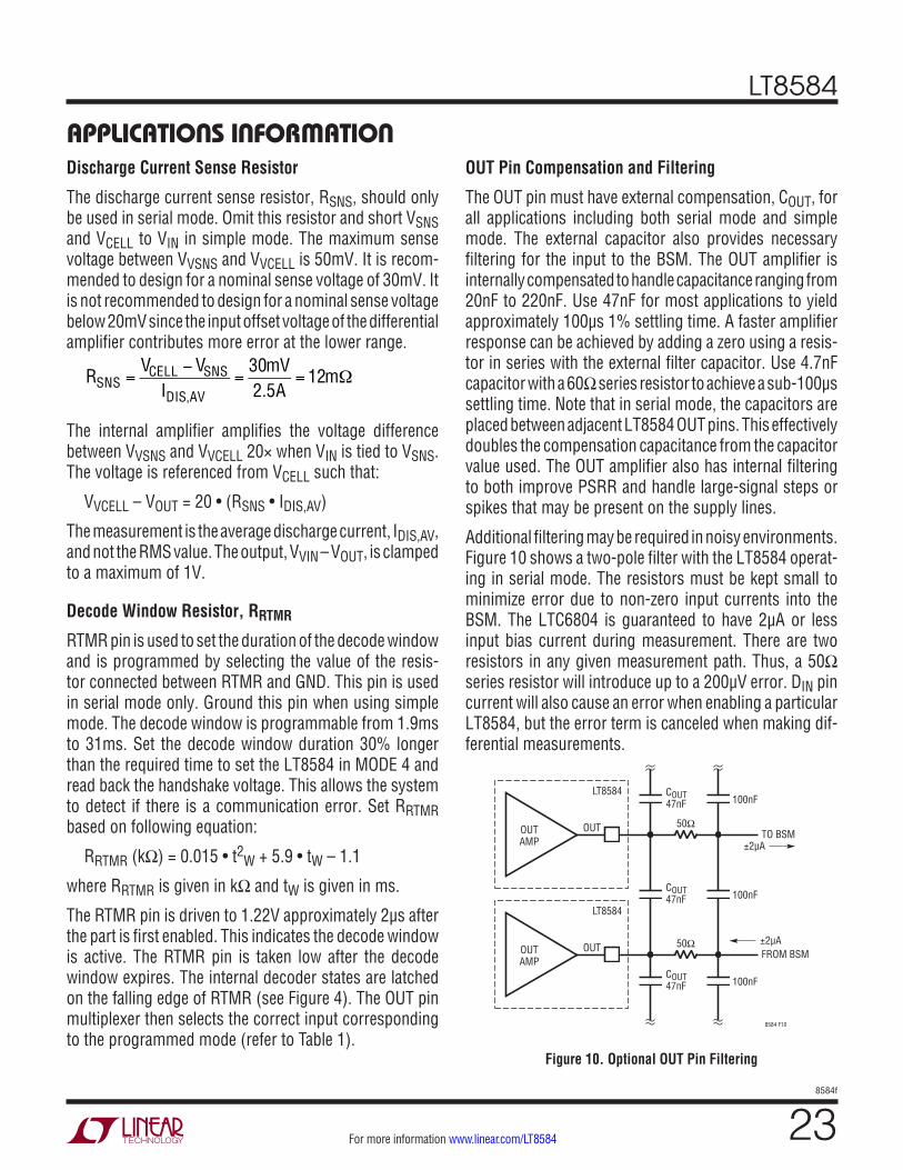
The OUT pin must have external compensation, COUT, for all applications including both serial mode and simple mode. The external capacitor also provides necessary filtering for the input to the BSM. The OUT amplifier is internally compensated to handle capacitance ranging from 20nF to 220nF. Use 47nF for most applications to yield approximately 100µs 1% settling time. A faster amplifier response can be achieved by adding a zero using a resis-tor in series with the external filter capacitor. Use 4.7nF capacitor with a 60Ω series resistor to achieve a sub-100µs settling time. Note that in serial mode, the capacitors are placed between adjacent LT8584 OUT pins. This effectively doubles the compensation capacitance from the capacitor value used. The OUT amplifier also has internal filtering to both improve PSRR and handle large-signal steps or spikes that may be present on the supply lines.
Additional filtering may be required in noisy environments. Figure 10 shows a two-pole filter with the LT8584 operat-ing in serial mode. The resistors must be kept small to minimize error due to non-zero input currents into the BSM. The LTC6804 is guaranteed to have 2µA or less input bias current during measurement. There are two resistors in any given measurement path. Thus, a 50Ω series resistor will introduce up to a 200µV error. DIN pin current will also cause an error when enabling a particular LT8584, but the error term is canceled when making dif-ferential measurements.
8584 F10
OUTAMP
LT8584
OUT 50Ω
COUT47nF 100nF
OUTAMP
LT8584
OUT 50Ω
COUT47nF 100nF
TO BSM±2µA
FROM BSM
COUT47nF 100nF
±2µA
Figure 10. Optional OUT Pin Filtering
LT8584
248584f
For more information www.linear.com/LT8584
applicaTions inForMaTionHOT SWAP™ PROTECTION
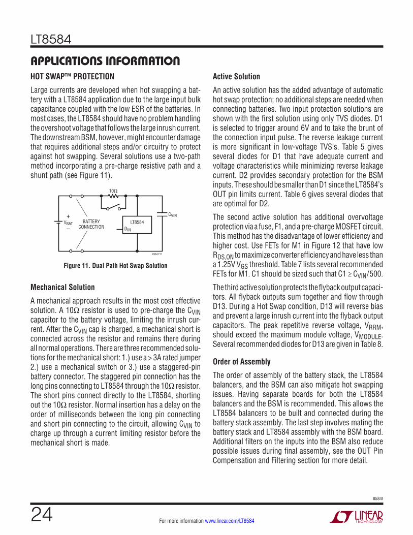
Large currents are developed when hot swapping a bat-tery with a LT8584 application due to the large input bulk capacitance coupled with the low ESR of the batteries. In most cases, the LT8584 should have no problem handling the overshoot voltage that follows the large inrush current. The downstream BSM, however, might encounter damage that requires additional steps and/or circuitry to protect against hot swapping. Several solutions use a two-path method incorporating a pre-charge resistive path and a shunt path (see Figure 11).
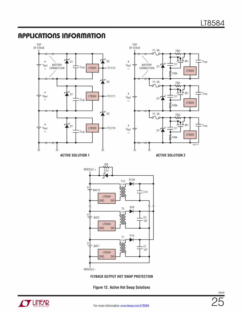
Active Solution
An active solution has the added advantage of automatic hot swap protection; no additional steps are needed when connecting batteries. Two input protection solutions are shown with the first solution using only TVS diodes. D1 is selected to trigger around 6V and to take the brunt of the connection input pulse. The reverse leakage current is more significant in low-voltage TVS’s. Table 5 gives several diodes for D1 that have adequate current and voltage characteristics while minimizing reverse leakage current. D2 provides secondary protection for the BSM inputs. These should be smaller than D1 since the LT8584’s OUT pin limits current. Table 6 gives several diodes that are optimal for D2.
The second active solution has additional overvoltage protection via a fuse, F1, and a pre-charge MOSFET circuit. This method has the disadvantage of lower efficiency and higher cost. Use FETs for M1 in Figure 12 that have low RDS,ON to maximize converter efficiency and have less than a 1.25V VGS threshold. Table 7 lists several recommended FETs for M1. C1 should be sized such that C1 ≥ CVIN/500.
The third active solution protects the flyback output capaci-tors. All flyback outputs sum together and flow through D13. During a Hot Swap condition, D13 will reverse bias and prevent a large inrush current into the flyback output capacitors. The peak repetitive reverse voltage, VRRM, should exceed the maximum module voltage, VMODULE. Several recommended diodes for D13 are given in Table 8.
Order of Assembly
The order of assembly of the battery stack, the LT8584 balancers, and the BSM can also mitigate hot swapping issues. Having separate boards for both the LT8584 balancers and the BSM is recommended. This allows the LT8584 balancers to be built and connected during the battery stack assembly. The last step involves mating the battery stack and LT8584 assembly with the BSM board. Additional filters on the inputs into the BSM also reduce possible issues during final assembly, see the OUT Pin Compensation and Filtering section for more detail.
8584 F11
CVIN
VBAT BATTERYCONNECTION
+
–
10Ω
LT8584DIN
Figure 11. Dual Path Hot Swap Solution
Mechanical Solution
A mechanical approach results in the most cost effective solution. A 10Ω resistor is used to pre-charge the CVIN capacitor to the battery voltage, limiting the inrush cur-rent. After the CVIN cap is charged, a mechanical short is connected across the resistor and remains there during all normal operations. There are three recommended solu-tions for the mechanical short: 1.) use a > 3A rated jumper 2.) use a mechanical switch or 3.) use a staggered-pin battery connector. The staggered pin connection has the long pins connecting to LT8584 through the 10Ω resistor. The short pins connect directly to the LT8584, shorting out the 10Ω resistor. Normal insertion has a delay on the order of milliseconds between the long pin connecting and short pin connecting to the circuit, allowing CVIN to charge up through a current limiting resistor before the mechanical short is made.
LT8584
258584f
For more information www.linear.com/LT8584
applicaTions inForMaTion
Figure 12. Active Hot Swap Solutions
8584 F12
CVIN
D1VBAT BATTERY
CONNECTION
+
– LT8584
TOPOF STACK
D2
TO C12
CVIN
D1VBAT
+
–LT8584
D2
TO C11
CVIN
D1VBAT
+
–LT8584
D2
TO C10
ACTIVE SOLUTION 1
FLYBACK OUTPUT HOT SWAP PROTECTION
CVIN
D1VBAT BATTERYCONNECTION
+
– LT8584
10Ω
TOPOF STACK
C1
ACTIVE SOLUTION 2
100k
M1
CVIN
D1VBAT
+
– LT8584
10ΩF1, 5A
F1, 5A
C1
100k
M1
CVIN
D1VBAT
+
– LT8584
10ΩF1, 5A
BAT12+
C1
100k
M1
LT8584
D12A
C12
T121:4
20k
D13MODULE +
MODULE –
GND SW
•
•
BAT2+
LT8584
D2A
C21µF
T21:4
GND SW
•
•
BAT1+
LT8584
D1A
C11µF
T11:4
GND SW
•
•
LT8584
268584f
For more information www.linear.com/LT8584
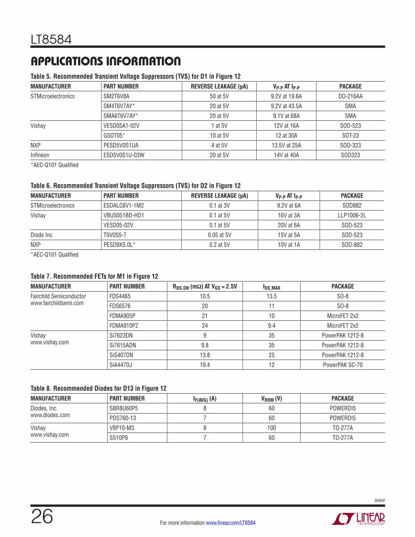
Table 7. Recommended FETs for M1 in Figure 12MANUFACTURER PART NUMBER RDS,ON (mΩ) AT VGS = 2.5V IDS,MAX PACKAGE
Fairchild Semiconductor www.fairchildsemi.com
FDS4465 10.5 13.5 SO-8
FDS6576 20 11 SO-8
FDMA905P 21 10 MicroFET 2x2
FDMA910PZ 24 9.4 MicroFET 2x2
Vishay www.vishay.com
Si7623DN 9 35 PowerPAK 1212-8
Si7615ADN 9.8 35 PowerPAK 1212-8
SiS407DN 13.8 25 PowerPAK 1212-8
SiA447DJ 19.4 12 PowerPAK SC-70
applicaTions inForMaTionTable 5. Recommended Transient Voltage Suppressors (TVS) for D1 in Figure 12MANUFACTURER PART NUMBER REVERSE LEAKAGE (µA) VP-P AT IP-P PACKAGE
STMicroelectronics SM2T6V8A 50 at 5V 9.2V at 19.6A DO-216AA
SM4T6V7AY* 20 at 5V 9.2V at 43.5A SMA
SMA6T6V7AY* 20 at 5V 9.1V at 68A SMA
Vishay VESD05A1-02V 1 at 5V 12V at 16A SOD-523
GSOT05* 10 at 5V 12 at 30A SOT-23
NXP PESD5V0S1UA 4 at 5V 13.5V at 25A SOD-323
Infineon ESD5V0S1U-03W 20 at 5V 14V at 40A SOD323
*AEC-Q101 Qualified
Table 6. Recommended Transient Voltage Suppressors (TVS) for D2 in Figure 12MANUFACTURER PART NUMBER REVERSE LEAKAGE (µA) VP-P AT IP-P PACKAGE
STMicroelectronics ESDALC6V1-1M2 0.1 at 3V 9.2V at 6A SOD882
Vishay VBUS051BD-HD1 0.1 at 5V 16V at 3A LLP1006-2L
VESD05-02V 0.1 at 5V 20V at 6A SOD-523
Diode Inc T5V0S5-7 0.05 at 5V 15V at 5A SOD-523
NXP PESD9X5.0L* 0.2 at 5V 10V at 1A SOD-882
*AEC-Q101 Qualified
Table 8. Recommended Diodes for D13 in Figure 12MANUFACTURER PART NUMBER IF(AVG) (A) VRRM (V) PACKAGE
Diodes, Inc. www.diodes.com
SBR8U60P5 8 60 POWERDI5
PDS760-13 7 60 POWERDI5
Vishay www.vishay.com
V8P10-M3 8 100 TO-277A
SS10P6 7 60 TO-277A
LT8584
278584f
For more information www.linear.com/LT8584
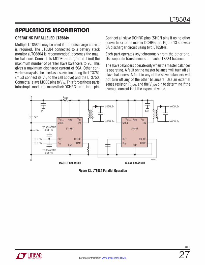
OPERATING PARALLELED LT8584s
Multiple LT8584s may be used if more discharge current is required. The LT8584 connected to a battery stack monitor (LTC6804 is recommended) becomes the mas-ter balancer. Connect its MODE pin to ground. Limit the maximum number of parallel slave balancers to 20. This gives a maximum discharge current of 50A. Other con-verters may also be used as a slave, including the LT3751 (must connect its VIN to the cell above) and the LT3750. Connect all slave MODE pins to VIN. This forces those parts into simple mode and makes their DCHRG pin an input pin.
applicaTions inForMaTionConnect all slave DCHRG pins (SHDN pins if using other converters) to the master DCHRG pin. Figure 13 shows a 5A discharger circuit using two LT8584s.
Each part operates asynchronously from the other one. Use separate transformers for each LT8584 balancer.
The slave balancers operate only when the master balancer is operating. A fault on the master balancer will turn off all slave balancers. A fault in any of the slave balancers will not turn off any of the other balancers. Use an external sense resistor, RSNS, and the VSNS pin to determine if the average current is at the expected value.
Figure 13. LT8584 Parallel Operation
LT8584
VINVSNS
RSNS
VCELL
GND
TO ADJACENTOUT PIN
TO ADJACENTOUT PIN
SW
DCHRG
RTMR
MODE
OUT
DIN
SLAVE BALANCERMASTER BALANCER
TO C PIN
TO S PIN
8584 F13
MODULE+
MODULE–
•
•
LT8584
VINVSNSVCELL
GND
SW
DCHRG
RTMR
MODE
OUT
DIN
MODULE+
MODULE–
•
•
BAT
BAT –
BAT –
+BAT –
LT8584
288584f
For more information www.linear.com/LT8584
applicaTions inForMaTion
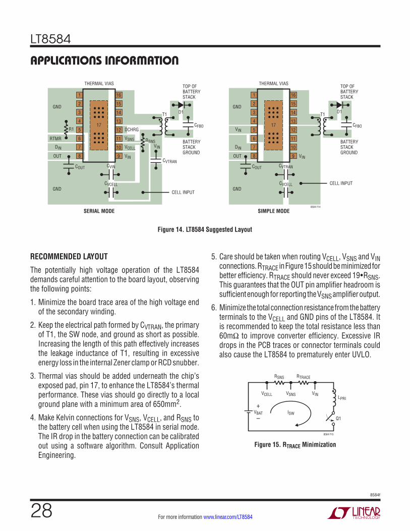
RECOMMENDED LAYOUT
The potentially high voltage operation of the LT8584 demands careful attention to the board layout, observing the following points:
1. Minimize the board trace area of the high voltage end of the secondary winding.
2. Keep the electrical path formed by CVTRAN, the primary of T1, the SW node, and ground as short as possible. Increasing the length of this path effectively increases the leakage inductance of T1, resulting in excessive energy loss in the internal Zener clamp or RCD snubber.
3. Thermal vias should be added underneath the chip’s exposed pad, pin 17, to enhance the LT8584’s thermal performance. These vias should go directly to a local ground plane with a minimum area of 650mm2.
4. Make Kelvin connections for VSNS, VCELL, and RSNS to the battery cell when using the LT8584 in serial mode. The IR drop in the battery connection can be calibrated out using a software algorithm. Consult Application Engineering.
5. Care should be taken when routing VCELL, VSNS and VIN connections. RTRACE in Figure 15 should be minimized for better efficiency. RTRACE should never exceed 19•RSNS. This guarantees that the OUT pin amplifier headroom is sufficient enough for reporting the VSNS amplifier output.
6. Minimize the total connection resistance from the battery terminals to the VCELL and GND pins of the LT8584. It is recommended to keep the total resistance less than 60mΩ to improve converter efficiency. Excessive IR drops in the PCB traces or connector terminals could also cause the LT8584 to prematurely enter UVLO.
Figure 14. LT8584 Suggested Layout
1
2
3
4
5
6
7
8
THERMAL VIAS
R1
16
15
14
13
12
11
10
9
17• •
CFBO
RSNSVIN
DCHRG
DIN
OUT
GND
GND
RTMR
CVCELL
CVINCOUT
VSNS
VCELL
VIN
BATTERYSTACKGROUND
TOP OFBATTERYSTACK
BATTERYSTACKGROUND
TOP OFBATTERYSTACK
D1
1
2
3
4
5
6
7
8
THERMAL VIAS
SERIAL MODE SIMPLE MODE
16
15
14
13
12
11
10
9
17• •
CFBO
T1T1
VIN
DIN
OUT
GND
GND
VIN
D1
8584 F14
CVTRAN
CELL INPUT
CVCELL
CVTRANCOUT
CELL INPUT
8584 F15
VBAT
+
–
RSNS
VCELL VSNS
ISW
RTRACE
VIN•
LPRI
Q1
Figure 15. RTRACE Minimization
LT8584
298584f
For more information www.linear.com/LT8584
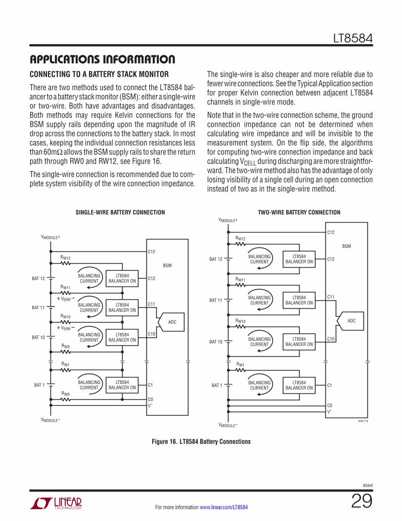
applicaTions inForMaTionCONNECTING TO A BATTERY STACK MONITOR
There are two methods used to connect the LT8584 bal-ancer to a battery stack monitor (BSM): either a single-wire or two-wire. Both have advantages and disadvantages. Both methods may require Kelvin connections for the BSM supply rails depending upon the magnitude of IR drop across the connections to the battery stack. In most cases, keeping the individual connection resistances less than 60mΩ allows the BSM supply rails to share the return path through RW0 and RW12, see Figure 16.
The single-wire connection is recommended due to com-plete system visibility of the wire connection impedance.
The single-wire is also cheaper and more reliable due to fewer wire connections. See the Typical Application section for proper Kelvin connection between adjacent LT8584 channels in single-wire mode.
Note that in the two-wire connection scheme, the ground connection impedance can not be determined when calculating wire impedance and will be invisible to the measurement system. On the flip side, the algorithms for computing two-wire connection impedance and back calculating VCELL during discharging are more straightfor-ward. The two-wire method also has the advantage of only losing visibility of a single cell during an open connection instead of two as in the single-wire method.
Figure 16. LT8584 Battery Connections
8584 F16
BAT 12
RW12
RW11
VERR
VMODULE+
VMODULE–
+ –
LT8584BALANCER ON
BALANCINGCURRENT
BAT 11
RW10
VERR+ –
BALANCINGCURRENT
BAT 10
RW9
RW1
BALANCINGCURRENT
BAT 1
RW0
LT8584BALANCER ON
BALANCINGCURRENT
BAT 12
RW12
LT8584BALANCER ON
BALANCINGCURRENT
BAT 11
RW11
LT8584BALANCER ON
BALANCINGCURRENT
BAT 10
RW10
LT8584BALANCER ON
BALANCINGCURRENT
BAT 1
RW1
LT8584BALANCER ON
BALANCINGCURRENT
LT8584BALANCER ON
LT8584BALANCER ON
C11
C12
C12
C10
C1
C0V–
ADC
BSM
TWO-WIRE BATTERY CONNECTIONSINGLE-WIRE BATTERY CONNECTION
C11
C12
C12
C10
C1
C0V–
ADC
BSM
VMODULE–
VMODULE+
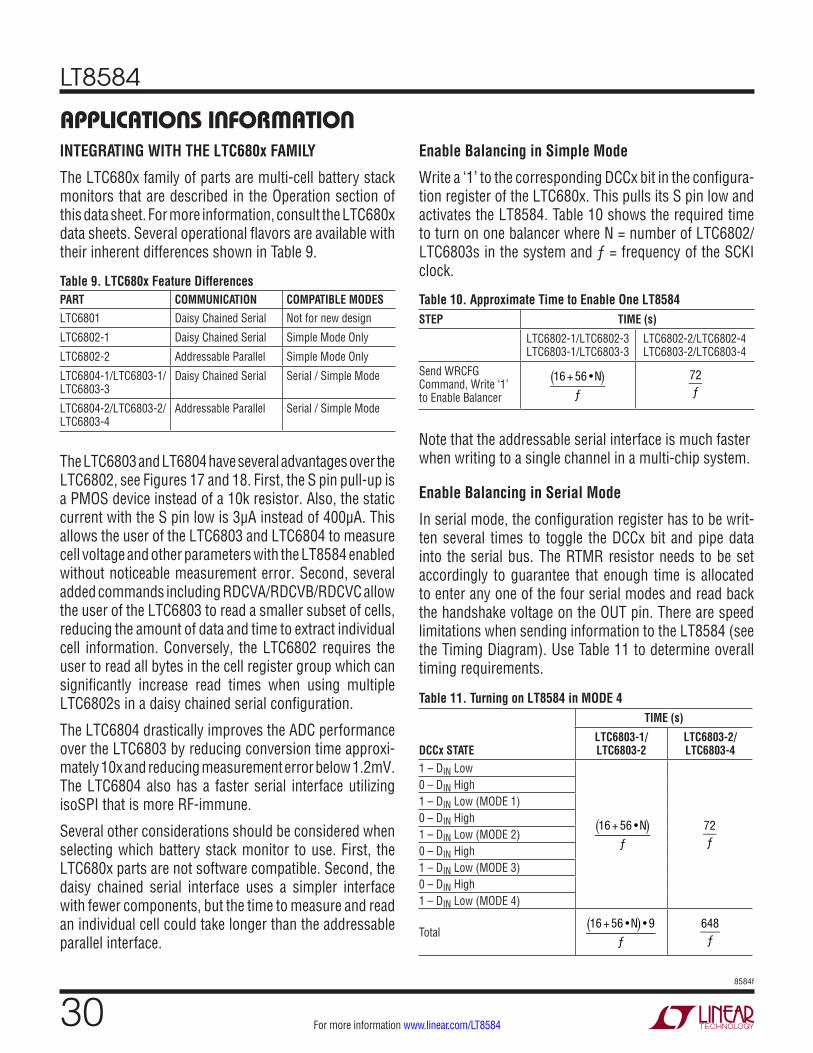
LT8584
308584f
For more information www.linear.com/LT8584
applicaTions inForMaTionINTEGRATING WITH THE LTC680x FAMILY
The LTC680x family of parts are multi-cell battery stack monitors that are described in the Operation section of this data sheet. For more information, consult the LTC680x data sheets. Several operational flavors are available with their inherent differences shown in Table 9.
Table 9. LTC680x Feature DifferencesPART COMMUNICATION COMPATIBLE MODESLTC6801 Daisy Chained Serial Not for new design
LTC6802-1 Daisy Chained Serial Simple Mode Only
LTC6802-2 Addressable Parallel Simple Mode Only
LTC6804-1/LTC6803-1/LTC6803-3
Daisy Chained Serial Serial / Simple Mode
LTC6804-2/LTC6803-2/LTC6803-4
Addressable Parallel Serial / Simple Mode
The LTC6803 and LT6804 have several advantages over the LTC6802, see Figures 17 and 18. First, the S pin pull-up is a PMOS device instead of a 10k resistor. Also, the static current with the S pin low is 3µA instead of 400µA. This allows the user of the LTC6803 and LTC6804 to measure cell voltage and other parameters with the LT8584 enabled without noticeable measurement error. Second, several added commands including RDCVA/RDCVB/RDCVC allow the user of the LTC6803 to read a smaller subset of cells, reducing the amount of data and time to extract individual cell information. Conversely, the LTC6802 requires the user to read all bytes in the cell register group which can significantly increase read times when using multiple LTC6802s in a daisy chained serial configuration.
The LTC6804 drastically improves the ADC performance over the LTC6803 by reducing conversion time approxi-mately 10x and reducing measurement error below 1.2mV. The LTC6804 also has a faster serial interface utilizing isoSPI that is more RF-immune.
Several other considerations should be considered when selecting which battery stack monitor to use. First, the LTC680x parts are not software compatible. Second, the daisy chained serial interface uses a simpler interface with fewer components, but the time to measure and read an individual cell could take longer than the addressable parallel interface.
Enable Balancing in Simple Mode
Write a ‘1’ to the corresponding DCCx bit in the configura-tion register of the LTC680x. This pulls its S pin low and activates the LT8584. Table 10 shows the required time to turn on one balancer where N = number of LTC6802/LTC6803s in the system and ƒ = frequency of the SCKI clock.
Table 10. Approximate Time to Enable One LT8584STEP TIME (s)
LTC6802-1/LTC6802-3 LTC6803-1/LTC6803-3
LTC6802-2/LTC6802-4 LTC6803-2/LTC6803-4
Send WRCFG Command, Write ‘1’ to Enable Balancer
16+ 56 •N( )ƒ
72ƒ
Note that the addressable serial interface is much faster when writing to a single channel in a multi-chip system.
Enable Balancing in Serial Mode
In serial mode, the configuration register has to be writ-ten several times to toggle the DCCx bit and pipe data into the serial bus. The RTMR resistor needs to be set accordingly to guarantee that enough time is allocated to enter any one of the four serial modes and read back the handshake voltage on the OUT pin. There are speed limitations when sending information to the LT8584 (see the Timing Diagram). Use Table 11 to determine overall timing requirements.
Table 11. Turning on LT8584 in MODE 4TIME (s)
DCCx STATELTC6803-1/ LTC6803-2
LTC6803-2/LTC6803-4
1 – DIN Low
16+ 56 •N( )ƒ
72ƒ
0 – DIN High 1 – DIN Low (MODE 1) 0 – DIN High 1 – DIN Low (MODE 2) 0 – DIN High 1 – DIN Low (MODE 3) 0 – DIN High 1 – DIN Low (MODE 4)
Total
16+ 56 •N( ) • 9ƒ
648ƒ
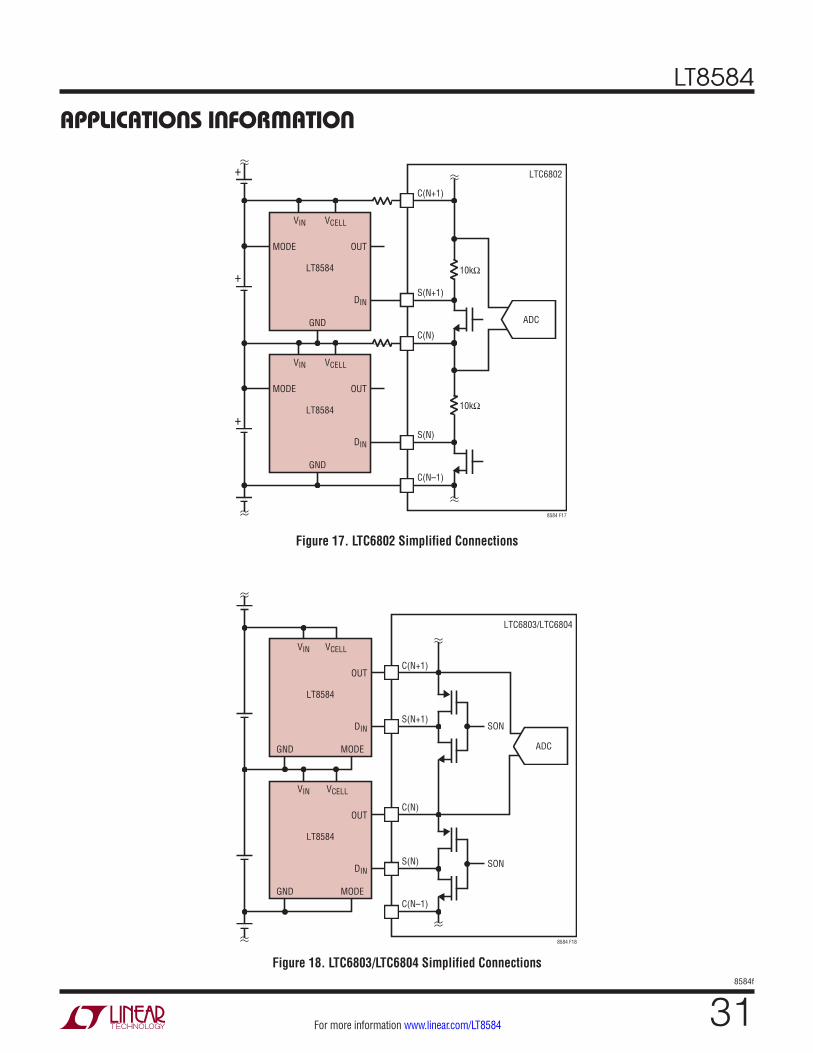
LT8584
318584f
For more information www.linear.com/LT8584
applicaTions inForMaTion
LT8584
VIN VCELL
GND
MODE
+
+
+
OUT
DIN
8584 F17
LTC6802
C(N+1)
10kΩ
S(N+1)
C(N)
LT8584
VIN VCELL
GND
MODE OUT
DIN
10kΩ
S(N)
C(N–1)
ADC
LT8584
VIN VCELL
MODEGND
OUT
DIN
8584 F18
LTC6803/LTC6804
C(N+1)
S(N+1)
C(N)
LT8584
VIN VCELL
GND
OUT
DIN
MODE
S(N) SON
C(N–1)
SON
ADC
Figure 17. LTC6802 Simplified Connections
Figure 18. LTC6803/LTC6804 Simplified Connections
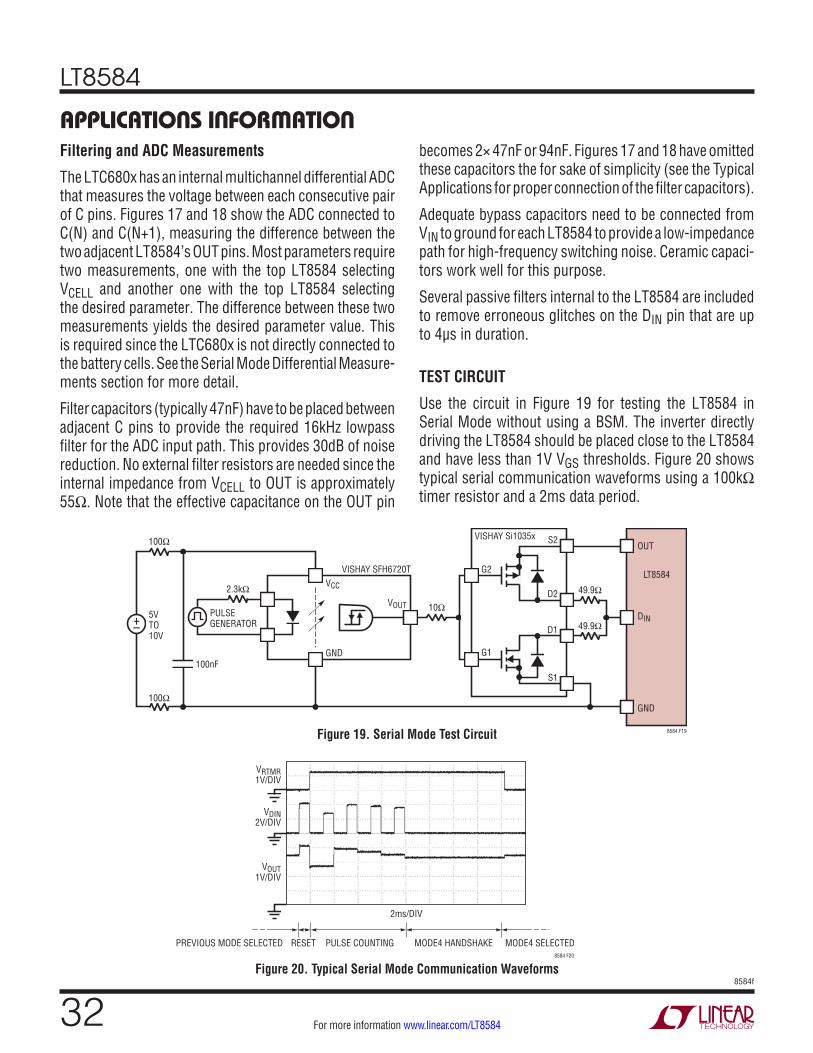
LT8584
328584f
For more information www.linear.com/LT8584
applicaTions inForMaTionFiltering and ADC Measurements
The LTC680x has an internal multichannel differential ADC that measures the voltage between each consecutive pair of C pins. Figures 17 and 18 show the ADC connected to C(N) and C(N+1), measuring the difference between the two adjacent LT8584’s OUT pins. Most parameters require two measurements, one with the top LT8584 selecting VCELL and another one with the top LT8584 selecting the desired parameter. The difference between these two measurements yields the desired parameter value. This is required since the LTC680x is not directly connected to the battery cells. See the Serial Mode Differential Measure-ments section for more detail.
Filter capacitors (typically 47nF) have to be placed between adjacent C pins to provide the required 16kHz lowpass filter for the ADC input path. This provides 30dB of noise reduction. No external filter resistors are needed since the internal impedance from VCELL to OUT is approximately 55Ω. Note that the effective capacitance on the OUT pin
becomes 2× 47nF or 94nF. Figures 17 and 18 have omitted these capacitors the for sake of simplicity (see the Typical Applications for proper connection of the filter capacitors).
Adequate bypass capacitors need to be connected from VIN to ground for each LT8584 to provide a low-impedance path for high-frequency switching noise. Ceramic capaci-tors work well for this purpose.
Several passive filters internal to the LT8584 are included to remove erroneous glitches on the DIN pin that are up to 4µs in duration.
TEST CIRCUIT
Use the circuit in Figure 19 for testing the LT8584 in Serial Mode without using a BSM. The inverter directly driving the LT8584 should be placed close to the LT8584 and have less than 1V VGS thresholds. Figure 20 shows typical serial communication waveforms using a 100kΩ timer resistor and a 2ms data period.
8584 F19
LT8584
VISHAY Si1035x
VISHAY SFH6720T
2.3kΩ
100Ω
100Ω
PULSEGENERATOR
5VTO10V
100nF
VCC
GND
VOUT
+–
10Ω
G2
G1
S2
D2
D1
S1
49.9Ω
49.9Ω
OUT
GND
DIN
Figure 19. Serial Mode Test Circuit
Figure 20. Typical Serial Mode Communication Waveforms
2ms/DIV
PULSE COUNTINGPREVIOUS MODE SELECTED MODE4 HANDSHAKE MODE4 SELECTED
VRTMR1V/DIV
VDIN2V/DIV
VOUT1V/DIV
8584 F20
RESET
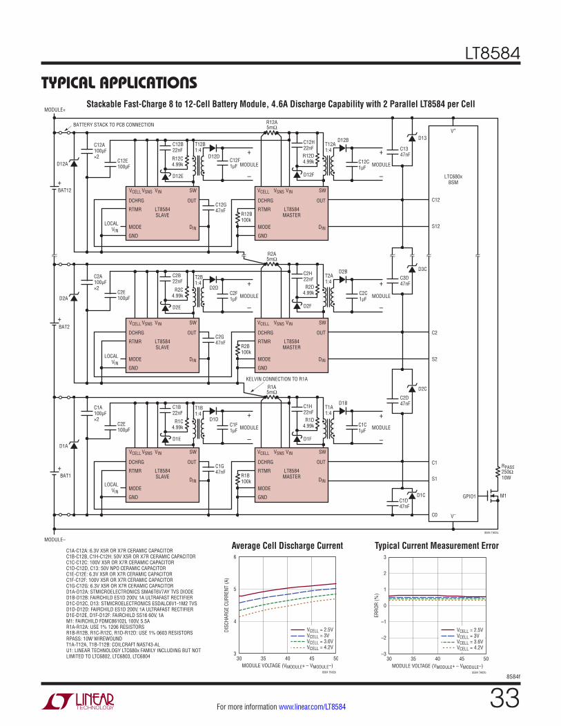
LT8584
338584f
For more information www.linear.com/LT8584
Typical applicaTionsStackable Fast-Charge 8 to 12-Cell Battery Module, 4.6A Discharge Capability with 2 Parallel LT8584 per Cell
•
•
LT8584SLAVE
VSNS VIN
LOCALVIN
LOCALVIN
LOCALVIN
SW
T12B1:4
C12F1µF MODULE
+
–
C12C1µF MODULE
+
–
D12D
VCELL
DCHRG
RTMR
MODE
GND
OUT
DIN
8584 TA02a
C12G47nF
•
•
T12A1:4
D12B
R12B100k
LT8584MASTER
R12A5mΩ
R2A5mΩ
R1A5mΩ
VSNS VIN SWVCELL
DCHRG
RTMR
MODE
GND
OUT
DIN
C12A100µF×2
C12E100µF
C12B22nF
D12E
R12C4.99k
BATTERY STACK TO PCB CONNECTION
D12A
BAT12
•
•
LT8584SLAVE
VSNS VIN SW
T2B1:4
C2F1µF MODULE
+
–
C2C1µF
C2E100µF
C3D47nF
D3C
MODULE
+
–
D2D
VCELL
DCHRG
RTMR
MODE
GND
OUT
DIN
C2G47nF
•
•
T2A1:4
D2B
R2B100k
LT8584MASTER
VSNS VIN SWVCELL
DCHRG
RTMR
MODE
GND
OUT
DIN
C2A100µF×2
D2A
•
•
LT8584SLAVE
C2E100µF
VSNS VIN SW
T1B1:4
C1F1µF MODULE
+
–
C1C1µF MODULE
+
–
D1D
VCELL
DCHRG
RTMR
MODE
GND
OUT
DIN
C1G47nF
•
•
T1A1:4
D1B
R1B100k
LT8584MASTER
VSNS VIN SWVCELL
DCHRG
RTMR
MODE
GND
OUT
DIN
C1A100µF×2
D1A
C1347nF
D13
C2D47nF
D2C
C1D47nF
D1C
LTC680xBSM
V+
V–
C12
S12
C2
S2
C1
C0
GPIO1 M1
RPASS250Ω10W
MODULE+
MODULE–
+
BAT2+
BAT1+
S1
KELVIN CONNECTION TO R1A
C1A-C12A: 6.3V X5R OR X7R CERAMIC CAPACITORC1B-C12B, C1H-C12H: 50V X5R OR X7R CERAMIC CAPACITORC1C-C12C: 100V X5R OR X7R CERAMIC CAPACITORC1D-C12D, C13: 50V NPO CERAMIC CAPACITOR C1E-C12E: 6.3V X5R OR X7R CERAMIC CAPACITORC1F-C12F: 100V X5R OR X7R CERAMIC CAPACITORC1G-C12G: 6.3V X5R OR X7R CERAMIC CAPACITOR D1A-D12A: STMICROELECTRONICS SMA6T6V7AY TVS DIODED1B-D12B: FAIRCHILD ES1D 200V, 1A ULTRAFAST RECTIFIER D1C-D12C, D13: STMICROELECTRONICS ESDALC6V1-1M2 TVS D1D-D12D: FAIRCHILD ES1D 200V, 1A ULTRAFAST RECTIFIERD1E-D12E, D1F-D12F: FAIRCHILD SS16 60V, 1AM1: FAIRCHILD FDMC86102L 100V, 5.5AR1A-R12A: USE 1% 1206 RESISTORSR1B-R12B, R1C-R12C, R1D-R12D: USE 1% 0603 RESISTORSRPASS: 10W WIREWOUND T1A-T12A, T1B-T12B: COILCRAFT NA5743-ALU1: LINEAR TECHNOLOGY LTC680x FAMILY INCLUDING BUT NOT LIMITED TO LTC6802, LTC6803, LTC6804
C12H22nF
D12F
R12D4.99k
C2B22nF
D2E
R2C4.99k
C2H22nF
D2F
R2D4.99k
C1B22nF
D1E
R1C4.99k
C1H22nF
D1F
R1D4.99k
Average Cell Discharge Current Typical Current Measurement Error
MODULE VOLTAGE (VMODULE+ – VMODULE–)30
DISC
HARG
E CU
RREN
T (A
)
6
5
4
335
8584 TA02b
504540
VCELL = 2.5VVCELL = 3VVCELL = 3.6VVCELL = 4.2V
MODULE VOLTAGE (VMODULE+ – VMODULE–)30
ERRO
R (%
)
3
2
1
0
–2
–1
–335
8584 TA02b
504540
VCELL = 2.5VVCELL = 3VVCELL = 3.6VVCELL = 4.2V
LT8584
348584f
For more information www.linear.com/LT8584
Typical applicaTionsStackable Fast-Charge 8 to 12-Cell Battery Module Application Notes
1. Channels 3 through 11 are omitted for clarity. These channels should be integrated similar to channel 2. Not all required components for the LTC680x are shown. Consult the LTC680x data sheet for recommended components and their connections.
2. Up to 20 LT8584 balancers may be connected in paral-lel to farther increase discharge current. The DCHRG pin can also drive an enable pin of a separate DC/DC converter like the LT3750 capacitor charger.
3. Multiple modules can be stacked in series to achieve a larger battery stack. Each module must contain an integer multiple of the total number of cells in the stack. For instance, an 80 cell stack should be constructed with 8 modules each having 10 cells. Use consecutive BSM channels starting with BSM channel 1when populating a module with less than 12 channels. Tie all unused LTC680x C pins to MODULE+.
4. Place one CnE capacitor close to the Master LT8584’s transformer primary, and place the other CnE capacitor close to the Slave LT8584’s transformer primary. The symbol ‘n’ denotes a particular channel ranging from 1 to 12.
5. Place RCD snubber composed of DnF, DnE, RnC, RnD, CnB, CnH, as close as possible to the respective trans-former primary. The symbol ‘n’ denotes a particular channel ranging from 1 to 12.
6. RPASS and M1 may be omitted for applications using only one module in the stack.
7. Each LT8584 channel should have no less than 650mm2
of PCB pad footprint for proper heat sinking.
8. Consult Application Engineering for proper communica-tion with LTC680x family of parts as well as a proper algorithm for extracting cell parameters.
9. Recommended for cells that operate within a 2.5V to 5.3V range.
Stackable 8 to 12-Cell Battery Module Application Notes
See the last page Typical Application.
1. Channels 4 through 11 are omitted for clarity. These channels should be integrated similar to channel 2. Not all required components for the LTC680x are shown. Consult the LTC680x data sheet for recommended components and their connections.
2. Multiple modules can be stacked in series to achieve a larger battery stack. Each module must contain an integer multiple of the total number of cells in the stack. For instance, an 80 cell stack should be constructed with 8 modules each having 10 cells. Use consecutive BSM channels starting with BSM channel 1 when populating a module with less than 12 channels. Tie all unused LTC680x C pins to MODULE+.
3. Place the CnB capacitor close to the LT8584’s trans-former primary. The RCD snubber composed of CnE, RnC and DnD should also be placed close the LT8584’s transformer primary. The symbol ‘n’ denotes a particular channel ranging from 1 to 12.
4. The BSM V+ pin may share cell 12’s positive battery connection, and the BSM V– pin may share cell 0’s negative battery connection as long as the summa-tion of each battery connection’s PCB trace, wire, and interconnection resistance is less than 60mΩ.
5. RPASS and M1 may be omitted for applications using only one module in the stack.
6. Each LT8584 channel should have no less than 650mm2
of PCB pad footprint for proper heat sinking.
7. Consult Application Engineering for proper communica-tion with LTC680x family of parts as well as a proper algorithm for extracting cell parameters.
8. Recommended for cells that operate within a 2.5V to 5.3V range.
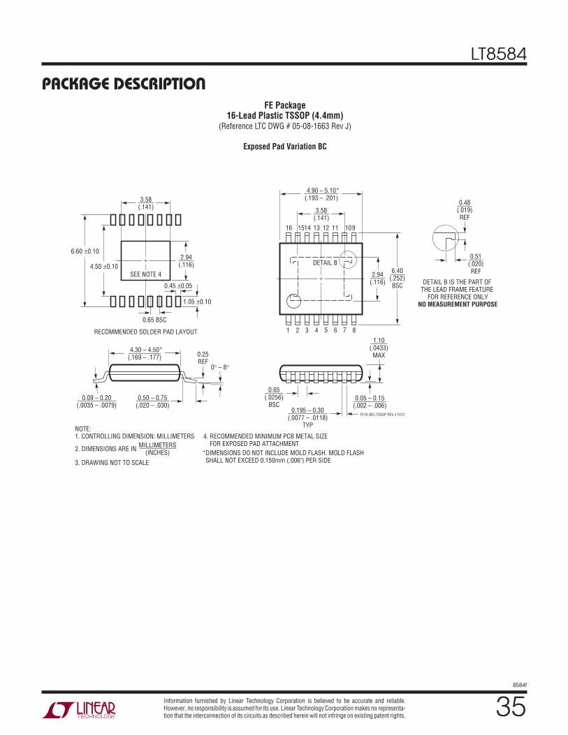
LT8584
358584f
For more information www.linear.com/LT8584
package DescripTionFE Package
16-Lead Plastic TSSOP (4.4mm)(Reference LTC DWG # 05-08-1663 Rev J)
Exposed Pad Variation BC
FE16 (BC) TSSOP REV J 1012
0.09 – 0.20(.0035 – .0079)
0° – 8°
0.25REF
0.50 – 0.75(.020 – .030)
4.30 – 4.50*(.169 – .177)
1 3 4 5 6 7 8
10
DETAIL B IS THE PART OF THE LEAD FRAME FEATURE
FOR REFERENCE ONLYNO MEASUREMENT PURPOSE
9
4.90 – 5.10*(.193 – .201)
16 1514 13 12 11
1.10(.0433)
MAX
0.05 – 0.15(.002 – .006)
0.65(.0256)
BSC
2.94(.116)
0.48(.019)REF
0.51(.020)REF
0.195 – 0.30(.0077 – .0118)
TYP
2RECOMMENDED SOLDER PAD LAYOUT
0.45 ±0.05
0.65 BSC
4.50 ±0.10
6.60 ±0.10
1.05 ±0.10
2.94(.116)
3.58(.141)
3.58(.141)
MILLIMETERS(INCHES) *DIMENSIONS DO NOT INCLUDE MOLD FLASH. MOLD FLASH
SHALL NOT EXCEED 0.150mm (.006") PER SIDE
NOTE:1. CONTROLLING DIMENSION: MILLIMETERS
2. DIMENSIONS ARE IN
3. DRAWING NOT TO SCALE
SEE NOTE 4
4. RECOMMENDED MINIMUM PCB METAL SIZE FOR EXPOSED PAD ATTACHMENT
6.40(.252)BSC
FE Package16-Lead Plastic TSSOP (4.4mm)
(Reference LTC DWG # 05-08-1663 Rev J)Exposed Pad Variation BC
DETAIL B
Information furnished by Linear Technology Corporation is believed to be accurate and reliable. However, no responsibility is assumed for its use. Linear Technology Corporation makes no representa-tion that the interconnection of its circuits as described herein will not infringe on existing patent rights.
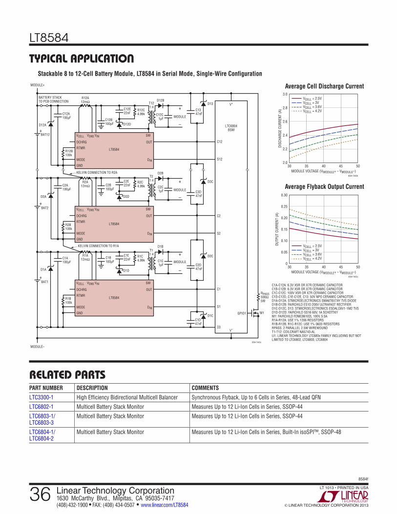
LT8584
368584f
For more information www.linear.com/LT8584
C12C1µF MODULE
+
–
8584 TA03a
•
•
T121:4
C12B100µF
D12B
C12E22nF
R12C4.99k
D12D
R12B100k
LT8584
R12A12mΩ
R2A12mΩ
VSNS VIN SWVCELL
DCHRG
RTMR
MODE
GND
OUT
DIN
C12A100µF
BATTERY STACK TO PCB CONNECTION
KELVIN CONNECTION TO R2A
D12A
BAT12
C2C1µF C3D
47nF
D3C
MODULE
+
–
•
•
T21:4
C2B100µF
D2B
R2B100k
LT8584
VSNS VIN SWVCELL
DCHRG
RTMR
MODE
GND
OUT
DIN
C2A100µF
D2A
C1C1µF
MODULE
+
–
•
•
T11:4
C1B100µF
D1B
R1B100k
LT8584
VSNS VIN SWVCELL
DCHRG
RTMR
MODE
GND
OUT
DIN
C1A100µF
D1A
C1347nF
D13
C2D47nF
D2C
C1D47nF
D1C
LTC6804BSM
V+
V–
C12
S12
C2
S2
C1
S1
C0
GPIO1 M1
RPASS500Ω5W
MODULE+
MODULE–
+
BAT2+
BAT1+
R1A12mΩ
KELVIN CONNECTION TO R1A
C1A-C12A: 6.3V X5R OR X7R CERAMIC CAPACITORC1B-C12B: 6.3V X5R OR X7R CERAMIC CAPACITORC1C-C12C: 100V X5R OR X7R CERAMIC CAPACITORC1D-C12D, C1E-C12E, C13: 50V NPO CERAMIC CAPACITOR D1A-D12A: STMICROELECTRONICS SMA6T6V7AY TVS DIODED1B-D12B: FAIRCHILD ES1D 200V ULTRAFAST RECTIFIERD1C-D12C, D13: STMICROELECTRONICS ESDALC6V1-1M2 TVS D1D-D12D: FAIRCHILD SS16 60V, 1A SCHOTTKYM1: FAIRCHILD FDMC86102L 100V, 5.5AR1A-R12A: USE 1% 1206 RESISTORSR1B-R12B, R1C-R12C: USE 1% 0603 RESISTORSRPASS: 2 PARALLEL 2.5W WIREWOUND T1-T12: COILCRAFT NA5743-ALU1: LINEAR TECHNOLOGY LTC680x FAMILY INCLUDING BUT NOT LIMITED TO LTC6802, LTC6803, LTC6804
C2E22nF
R2C4.99k
D2D
C1E22nF
R1C4.99k
D1D
relaTeD parTs
Typical applicaTion
PART NUMBER DESCRIPTION COMMENTS
LTC3300-1 High Efficiency Bidirectional Multicell Balancer Synchronous Flyback, Up to 6 Cells in Series, 48-Lead QFN
LTC6802-1 Multicell Battery Stack Monitor Measures Up to 12 Li-Ion Cells in Series, SSOP-44
LTC6803-1/LTC6803-3
Multicell Battery Stack Monitor Measures Up to 12 Li-Ion Cells in Series, SSOP-44
LTC6804-1/ LTC6804-2
Multicell Battery Stack Monitor Measures Up to 12 Li-Ion Cells in Series, Built-In isoSPI™, SSOP-48
Stackable 8 to 12-Cell Battery Module, LT8584 in Serial Mode, Single-Wire Configuration
Average Cell Discharge Current
MODULE VOLTAGE (VMODULE+ – VMODULE–)30
DISC
HARG
E CU
RREN
T (A
)
3.0
2.4
2.2
2.8
2.6
2.035
8584 TA03b
504540
VCELL = 2.5VVCELL = 3VVCELL = 3.6VVCELL = 4.2V
MODULE VOLTAGE (VMODULE+ – VMODULE–)30
OUTP
UT C
URRE
NT (A
)
0.30
0.10
0.05
0.20
0.25
0.15
035
8584 TA03c
504540
VCELL = 2.5VVCELL = 3VVCELL = 3.6VVCELL = 4.2V
Average Flyback Output Current
LINEAR TECHNOLOGY CORPORATION 2013
LT 1013 • PRINTED IN USALinear Technology Corporation1630 McCarthy Blvd., Milpitas, CA 95035-7417(408) 432-1900 FAX: (408) 434-0507 www.linear.com/LT8584