Embed Size (px)
Citation preview
LTC2313-12
1231312fb
For more information www.linear.com/LTC2313-12
TYPICAL APPLICATION
FEATURES DESCRIPTION
12-Bit, 2.5Msps Serial Sampling ADC in TSOT
The LTC®2313-12 is a 12-bit, 2.5Msps, serial sampling A/D converter that draws only 5mA from a single 3V or 5V supply. The LTC2313-12 contains an integrated low drift reference and reference buffer providing a low cost, high performance (20ppm/°C maximum) and space saving solution. The LTC2313-12 achieves outstanding AC performance of 72.6dB SINAD and –84dB THD while sampling at 2.5Msps. The extremely high sample rate-to-power ratio makes the LTC2313-12 ideal for compact, low power, high speed systems. The supply current decreases at lower sampling rates as the device automatically enters nap mode after conversions.
The LTC2313-12 has a high speed SPI-compatible serial interface that supports 1.8V, 2.5V, 3V and 5V logic. The fast 2.5Msps throughput with no cycle latency makes the LTC2313-12 ideally suited for a wide variety of high speed applications.Complete 14-/12-Bit Pin-Compatible SAR ADC Family
500ksps 2.5Msps 4.5Msps 5Msps
14-Bit LTC2312-14 LTC2313-14 LTC2314-14
12-Bit LTC2312-12 LTC2313-12 LTC2315-12
Power 3V/5V 9mW/15mW 14mW/25mW 18mW/31mW 19mW/32mW
APPLICATIONS
n 2.5Msps Throughput Rate n No Cycle Latency n Guaranteed 12-Bit No Missing Codes n Single 3V or 5V Supply n Low Noise: 73dB SNR n Low Power: 14mW at 2.5Msps and 3V Supply n Low Drift (20ppm/°C Maximum) 2.048V or 4.096V
Internal Reference n Sleep Mode with < 1µA Typical Supply Current n Nap Mode with Quick Wake-Up < 1 Conversion n Separate 1.8V to 5V Digital I/O Supply n High Speed SPI-Compatible Serial I/O n Guaranteed Operation from –40°C to 125°C n 8-Lead TSOT-23 Package
n Communication Systems n High Speed Data Acquisition n Handheld Terminal Interface n Medical Imaging n Uninterrupted Power Supplies n Battery Operated Systems n Automotive
L, LT, LTC, LTM, Linear Technology and the Linear logo are registered trademarks of Linear Technology Corporation. All other trademarks are the property of their respective owners.
5V Supply, Internal Reference, 2.5Msps, 12-Bit Sampling ADC 16k Point FFT, fS = 2.5Msps, fIN = 497kHz
231312 TA01bINPUT FREQUENCY (kHz)
AMPL
ITUD
E (d
BFS)
0 1000500250 750
0
–20
–40
–60
–80
–100
–120
–140
–160
VDD = 5VSNR = 73dBFS
SINAD = 72.6dBFSTHD = –84dBSFDR = 87dB
SERIAL DATA LINK TOASIC, PLD, MPU, DSPOR SHIFT REGISTERS
ANALOG INPUT0V TO 4.096V
5V
2.2µF
2.2µF
2.2µF
231312 TA01a
GND
VDD
REF
AIN OVDD
SCK
CONV
SDO
LTC2313-12
DIGITAL OUTPUT SUPPLY1.8V TO 5V
LTC2313-12
2231312fb
For more information www.linear.com/LTC2313-12
PIN CONFIGURATIONABSOLUTE MAXIMUM RATINGS
Supply Voltage (VDD, OVDD) .......................................6VReference (REF) and Analog Input (AIN) Voltage(Note 3) ......................................(–0.3V) to (VDD + 0.3V)Digital Input Voltage (Note 3) ... (–0.3V) to (OVDD + 0.3V)Digital Output Voltage ............. (–0.3V) to (OVDD + 0.3V)Power Dissipation ...............................................100mWOperating Temperature Range LTC2313C ................................................ 0°C to 70°C LTC2313I..............................................–40°C to 85°C LTC2313H .......................................... –40°C to 125°CStorage Temperature Range .................. –65°C to 150°CLead Temperature Range (Soldering, 10 sec) ........ 300°C
(Notes 1, 2)
1234
8765
TOP VIEW
TS8 PACKAGE8-LEAD PLASTIC TSOT-23
CONVSCKSDOOVDD
VDDREF
GNDAIN
TJMAX = 150°C, θJA = 195°C/W
ORDER INFORMATIONLead Free FinishTAPE AND REEL (MINI) TAPE AND REEL PART MARKING* PACKAGE DESCRIPTION TEMPERATURE RANGE
LTC2313CTS8-12#TRMPBF LTC2313CTS8-12#TRPBF LTFZJ 8-Lead Plastic TSOT-23 0°C to 70°C
LTC2313ITS8-12#TRMPBF LTC2313ITS8-12#TRPBF LTFZJ 8-Lead Plastic TSOT-23 –40˚C to 85˚C
LTC2313HTS8-12#TRMPBF LTC2313HTS8-12#TRPBF LTFZJ 8-Lead Plastic TSOT-23 –40˚C to 125˚CTRM = 500 pieces. *Temperature grades are identified by a label on the shipping container.Consult LTC Marketing for parts specified with wider operating temperature ranges. Consult LTC Marketing for information on lead based finish parts.For more information on lead free part marking, go to: http://www.linear.com/leadfree/ For more information on tape and reel specifications, go to: http://www.linear.com/tapeandreel/
LTC2313-12
3231312fb
For more information www.linear.com/LTC2313-12
ELECTRICAL CHARACTERISTICS
CONVERTER CHARACTERISTICS
DYNAMIC ACCURACY
SYMBOL PARAMETER CONDITIONS MIN TYP MAX UNITS
VAIN Absolute Input Range l –0.05 VDD + 0.05 V
VIN Input Voltage Range (Note 11) l 0 VREF V
IIN Analog Input DC Leakage Current l –1 1 µA
CIN Analog Input Capacitance Sample Mode Hold Mode
13 3
pF pF
SYMBOL PARAMETER CONDITIONS MIN TYP MAX UNITS
Resolution l 12 Bits
No Missing Codes l 12 Bits
Transition Noise (Note 6) 0.33 LSBRMS
INL Integral Linearity Error VDD = 5V (Note 5) VDD = 3V (Note 5)
l
l
–1.25 –1.5
±0.3 ±0.4
1.25 1.5
LSB LSB
DNL Differential Linearity Error VDD = 5V VDD = 3V
l
l
–0.99 –0.99
±0.2 ±0.25
0.99 0.99
LSB LSB
Offset Error VDD = 5V VDD = 3V
l
l
–3.5 –5
±0.2 ±0.5
3.5 5
LSB LSB
Full-Scale Error VDD = 5V VDD = 3V
l
l
–7 –10
±1 ±1.5
7 10
LSB LSB
Total Unadjusted Error VDD = 5V VDD = 3V
l
l
–8 –11
±1.5 ±2
8 11
LSB LSB
SYMBOL PARAMETER CONDITIONS MIN TYP MAX UNITS
SINAD Signal-to-(Noise + Distortion) Ratio fIN = 497kHz, VDD = 5V fIN = 497kHz, VDD = 3V
l
l
70 67.5
72.6 70.3
dB dB
SNR Signal-to-Noise Ratio fIN = 497kHz, VDD = 5V fIN = 497kHz, VDD = 3V
l
l
70.5 68
73 70.6
dB dB
THD Total Harmonic Distortion First 5 Harmonics
fIN = 497kHz, VDD = 5V fIN = 497kHz, VDD = 3V
l
l
–84 –84
–76 –76
dB dB
SFDR Spurious Free Dynamic Range fIN = 497kHz, VDD = 5V fIN = 497kHz, VDD = 3V
l
l
78 77
87 87
dB dB
IMD Intermodulation Distortion 2nd Order Terms 3rd Order Terms
fIN1 = 255kHz, fIN2 = 285kHz, AIN1, AIN2 = –7dBFS
–80.4 –91.8
dBc dBc
Full Power Bandwidth At 3dB At 0.1dB
130 20
MHz MHz
–3dB Input Linear Bandwidth SINAD ≥ 68dB 5 MHz
tAP Aperture Delay 1 ns
tJITTER Aperture Jitter 10 psRMS
The l denotes the specifications which apply over the full operating temperature range, otherwise specifications are at TA = 25°C. (Note 4)
The l denotes the specifications which apply over the full operating temperature range, otherwise specifications are at TA = 25°C. (Note 4)
The l denotes the specifications which apply over the full operating temperature range, otherwise specifications are at TA = 25°C and AIN = –1dBFS. (Note 4)
LTC2313-12
4231312fb
For more information www.linear.com/LTC2313-12
REFERENCE INPUT/OUTPUT
POWER REQUIREMENTS
DIGITAL INPUTS AND DIGITAL OUTPUTS
SYMBOL PARAMETER CONDITIONS MIN TYP MAX UNITS
VREF VREF Output Voltage 2.7V ≤ VDD ≤ 3.6V 4.75 ≤ VDD ≤ 5.25V
l
l
2.040 4.080
2.048 4.096
2.056 4.112
V V
VREF Temperature Coefficient l 7 20 ppm/°C
VREF Output Resistance Normal Operation, ILOAD = 0mA to 5mA Overdrive Condition (VREFIN ≥ VREFOUT + 50mV)
1 52
Ω kΩ
VREF Line Regulation 2.7V ≤ VDD ≤ 3.6V 4.75 ≤ VDD ≤ 5.25V
0.4 0.2
mV/V mV/V
VREF 2.048V/4.096V Supply Threshold 4.15 V
VREF 2.048V/4.096V Supply Threshold Hysteresis 150 mV
VREF Input Voltage Range (External Reference Input)
2.7V ≤ VDD ≤ 3.6V 4.75 ≤ VDD ≤ 5.25V
l
l
VREF + 50mV VREF + 50mV
VDD 4.3
V V
SYMBOL PARAMETER CONDITIONS MIN TYP MAX UNITS
VDD Supply Voltage 3V Operational Range 5V Operational Range
l
l
2.7
4.75
3 5
3.6
5.25
V V
OVDD Digital Output Supply Voltage l 1.71 5.25 V
ITOTAL = IVDD + IOVDD
Supply Current, Static Mode Operational Mode Nap Mode Sleep Mode
CONV = 0V, SCK = 0V l
l
l
3.4 5 2
0.2
4.4 6 5
mA mA mA µA
PD Power Dissipation, Static Mode Operational Mode Nap Mode Sleep Mode
CONV = 0V, SCK = 0V l
l
l
17 25 10 1
22 30
25
mW mW mW µW
SYMBOL PARAMETER CONDITIONS MIN TYP MAX UNITS
VIH High Level Input Voltage l 0.8 • OVDD V
VIL Low Level Input Voltage l 0.2 • OVDD V
IIN Digital Input Current VIN = 0V to OVDD l –10 10 μA
CIN Digital Input Capacitance 5 pF
VOH High Level Output Voltage IO = –500µA (Source) l OVDD–0.2 V
VOL Low Level Output Voltage IO = 500µA (Sink) l 0.2 V
IOZ Hi-Z Output Leakage Current VOUT = 0V to OVDD, CONV = High l –10 10 µA
COZ Hi-Z Output Capacitance CONV = High 4 pF
ISOURCE Output Source Current VOUT = 0V, OVDD = 1.8V –20 mA
ISINK Output Sink Current VOUT = OVDD = 1.8V 20 mA
The l denotes the specifications which apply over the full operating temperature range, otherwise specifications are at TA = 25°C. (Note 4)
The l denotes the specifications which apply over the full operating temperature range, otherwise specifications are at TA = 25°C. (Note 4)
The l denotes the specifications which apply over the full operating temperature range, otherwise specifications are at TA = 25°C. (Note 4)
LTC2313-12
5231312fb
For more information www.linear.com/LTC2313-12
ADC TIMING CHARACTERISTICS
SYMBOL PARAMETER CONDITIONS MIN TYP MAX UNITS
fSAMPLE(MAX) Maximum Sampling Frequency (Notes 7, 8) l 2.5 MHz
fSCK Shift Clock Frequency (Notes 7, 8) l 90 MHz
tSCK Shift Clock Period l 11.1 ns
tTHROUGHPUT Minimum Throughput Time, tACQ + tCONV l 400 ns
tCONV Conversion Time l 247 ns
tACQ Acquisition Time l 153 ns
t1 Minimum CONV Pulse Width (Note 7) Valid for Nap and Sleep Mode Only l 10 ns
t2 SCK↑ Setup Time After CONV↓ (Note 7) l 10 ns
t3 SDO Enable Time After CONV↓ (Notes 7, 8) l 10 ns
t4 SDO Data Valid Access Time after SCK↓ (Notes 7, 8, 9) l 9.1 ns
t5 SCK Low Time l 4 ns
t6 SCK High Time l 4 ns
t7 SDO Data Valid Hold Time After SCK↓ (Notes 7, 8, 9) l 1 ns
t8 SDO into Hi-Z State Time After CONV↑ (Notes 7, 8, 10) l 3 10 ns
t9 CONV↑ Quiet Time After 12th SCK↓ (Note 7) l 15 ns
tWAKE_NAP Power-Up Time from Nap Mode See Nap Mode Section 50 ns
tWAKE_SLEEP Power-Up Time from Sleep Mode See Sleep Mode Section 1.1 ms
The l denotes the specifications which apply over the full operating temperature range, otherwise specifications are at TA = 25°C. (Note 4)
Note 1. Stresses beyond those listed under Absolute Maximum Ratings may cause permanent damage to the device. Exposure to any Absolute Maximum Rating condition for extended periods may affect device reliability and lifetime.Note 2. All voltage values are with respect to ground.Note 3. When these pin voltages are taken below ground or above VDD (AIN, REF) or OVDD (SCK, CONV, SDO) they will be clamped by internal diodes. This product can handle input currents up to 100mA below ground or above VDD or OVDD without latch-up.Note 4. VDD = 5V, OVDD = 2.5V, fSMPL = 2.5MHz, fSCK = 90MHz, AIN = –1dBFS and internal reference unless otherwise noted.Note 5. Integral nonlinearity is defined as the deviation of a code from a straight line passing through the actual endpoints of the transfer curve. The deviation is measured from the center of the quantization band.
Note 6. Typical RMS noise at code transitions.Note 7. Parameter tested and guaranteed at OVDD = 2.5V. All input signals are specified with tr = tf = 1ns (10% to 90% of OVDD) and timed from a voltage level of OVDD/2.Note 8. All timing specifications given are with a 10pF capacitance load. Load capacitances greater than this will require a digital buffer.Note 9. The time required for the output to cross the VOH or VOL voltage.Note 10. Guaranteed by design, not subject to test. Note 11. Recommended operating conditions.
LTC2313-12
6231312fb
For more information www.linear.com/LTC2313-12
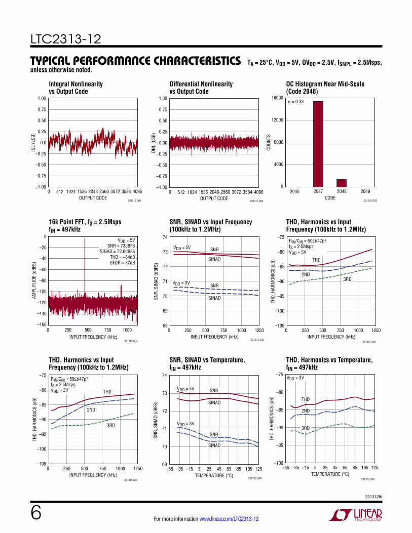
TYPICAL PERFORMANCE CHARACTERISTICS
16k Point FFT, fS = 2.5Msps fIN = 497kHz
SNR, SINAD vs Input Frequency (100kHz to 1.2MHz)
THD, Harmonics vs Input Frequency (100kHz to 1.2MHz)
THD, Harmonics vs Input Frequency (100kHz to 1.2MHz)
SNR, SINAD vs Temperature, fIN = 497kHz
THD, Harmonics vs Temperature, fIN = 497kHz
Integral Nonlinearity vs Output Code
Differential Nonlinearity vs Output Code
DC Histogram Near Mid-Scale (Code 2048)
TA = 25°C, VDD = 5V, OVDD = 2.5V, fSMPL = 2.5Msps, unless otherwise noted.
OUTPUT CODE0
–1.00
–0.50
–0.75
INL
(LSB
)
–0.25
0.25
0.0
0.50
0.75
1.00
1024 2048 3072 4096512 1536 2560 3584
231312 G01 OUTPUT CODE
–1.00
–0.75
–0.50
DNL
(LSB
)–0.25
0.25
0.00
0.50
0.75
1.00
231312 G02
0 1024 2048 3072 4096512 1536 2560 3584CODE
COUN
TS
2047 2048
231312 G03
2046 2049
σ = 0.33
0
4000
8000
16000
12000
TEMPERATURE (°C)–55 –35
–100
–95
THD,
HAR
MON
ICS
(dB)
–90
–85
–80
–75
–15 5 25 45 65 85 105 125
231312 G09
THD
3RD
2ND
VDD = 3V
INPUT FREQUENCY (kHz)0
68
69
SNR,
SIN
AD (d
BFS)
71
70
72
73
74
500250 750 1000 1250
231312 G05
SINAD
SNR
SINAD
SNR
VDD = 5V
VDD = 3V
INPUT FREQUENCY (kHz)0
–105
–95
–100
THD,
HAR
MON
ICS
(dB)
–90
–85
–80
–75
500250 750 1000 1250
231312 G06
THD
2ND3RD
RIN/CIN = 50Ω/47pFfS = 2.5MspsVDD = 5V
INPUT FREQUENCY (kHz)0
–105
–95
–100
THD,
HAR
MON
ICS
(dB)
–90
–85
–80
–75
500250 750 1000 1250
231312 G07
THD
2ND
3RD
RIN/CIN = 50Ω/47pFfS = 2.5MspsVDD = 3V
69
71
70
72
73
74
TEMPERATURE (°C)–55 –35
SNR,
SIN
AD (d
BFS)
–15 5 25 45 65 85 105 125
231312 G08
SNR
SNR
SINAD
SINAD
VDD = 5V
VDD = 3V
231312 G04INPUT FREQUENCY (kHz)
AMPL
ITUD
E (d
BFS)
0 1000500250 750
0
–20
–40
–60
–80
–100
–120
–140
–160
VDD = 5VSNR = 73dBFS
SINAD = 72.6dBFSTHD = –84dBSFDR = 87dB
LTC2313-12
7231312fb
For more information www.linear.com/LTC2313-12
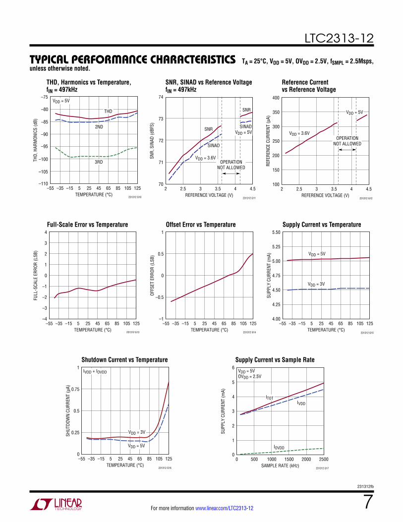
TYPICAL PERFORMANCE CHARACTERISTICS
Supply Current vs Temperature
Shutdown Current vs Temperature Supply Current vs Sample Rate
Reference Current vs Reference Voltage
Full-Scale Error vs Temperature Offset Error vs Temperature
SNR, SINAD vs Reference Voltage fIN = 497kHz
THD, Harmonics vs Temperature, fIN = 497kHz
TA = 25°C, VDD = 5V, OVDD = 2.5V, fSMPL = 2.5Msps, unless otherwise noted.
TEMPERATURE (°C)–55
–1
OFFS
ET E
RROR
(LSB
)
0
–0.5
0.5
1
–35 –15 5 4525 8565 105 125
231312 G14
TEMPERATURE (°C)–550
SHUT
DOW
N CU
RREN
T (µ
A)
0.25
0.5
1
0.75
–35 –15 5 4525 8565 105 125
231312 G16
VDD = 5V
VDD = 3V
IVDD + IOVDD
REFERENCE VOLTAGE (V)2
70
SNR,
SIN
AD (d
BFS)
71
72
74
73
2.5 3 3.5 4 4.5
231312 G11
SNR
SNR
SINAD
SINAD
VDD = 3.6VOPERATION
NOT ALLOWED
VDD = 5V
TEMPERATURE (°C)–55
–4
FULL
-SCA
LE E
RROR
(LSB
)
–1
0
–3
–2
1
2
3
4
–35 –15 5 4525 8565 105 125
231312 G13TEMPERATURE (°C)
–554.00
SUPP
LY C
URRE
NT (m
A)4.75
4.50
4.25
5.00
5.50
5.25
–35 –15 5 4525 8565 105 125
231312 G15
VDD = 5V
VDD = 3V
TEMPERATURE (°C)–55 –35
–110
–100
–105
–95
THD,
HAR
MON
ICS
(dB)
–90
–85
–80
–75
–15 5 25 45 65 85 105 125
231312 G10
THD
3RD
2ND
VDD = 5V
REFERENCE VOLTAGE (V)2
100
REFE
RENC
E CU
RREN
T (µ
A)
200
150
250
300
350
400
2.5 3 3.5 4 4.5
231312 G12
VDD = 3.6VOPERATION
NOT ALLOWED
VDD = 5V
SAMPLE RATE (kHz)0
0
SUPP
LY C
URRE
NT (m
A)
2
4
5
3
1
6
500 1000 1500 2000 2500
231312 G17
ITOTIVDD
VDD = 5VOVDD = 2.5V
IOVDD
LTC2313-12
8231312fb
For more information www.linear.com/LTC2313-12
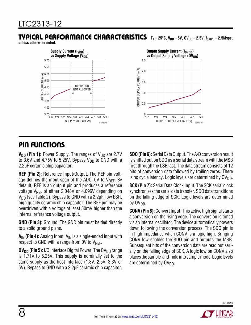
TA = 25°C, VDD = 5V, OVDD = 2.5V, fSMPL = 2.5Msps, unless otherwise noted.
PIN FUNCTIONSVDD (Pin 1): Power Supply. The ranges of VDD are 2.7V to 3.6V and 4.75V to 5.25V. Bypass VDD to GND with a 2.2µF ceramic chip capacitor.
REF (Pin 2): Reference Input/Output. The REF pin volt-age defines the input span of the ADC, 0V to VREF. By default, REF is an output pin and produces a reference voltage VREF of either 2.048V or 4.096V depending on VDD (see Table 2). Bypass to GND with a 2.2µF, low ESR, high quality ceramic chip capacitor. The REF pin may be overdriven with a voltage at least 50mV higher than the internal reference voltage output.
GND (Pin 3): Ground. The GND pin must be tied directly to a solid ground plane.
AIN (Pin 4): Analog Input. AIN is a single-ended input with respect to GND with a range from 0V to VREF.
OVDD (Pin 5): I/O Interface Digital Power. The OVDD range is 1.71V to 5.25V. This supply is nominally set to the same supply as the host interface (1.8V, 2.5V, 3.3V or 5V). Bypass to GND with a 2.2µF ceramic chip capacitor.
SDO (Pin 6): Serial Data Output. The A/D conversion result is shifted out on SDO as a serial data stream with the MSB first through the LSB last. The data stream consists of 12 bits of conversion data followed by trailing zeros. There is no cycle latency. Logic levels are determined by OVDD.
SCK (Pin 7): Serial Data Clock Input. The SCK serial clock synchronizes the serial data transfer. SDO data transitions on the falling edge of SCK. Logic levels are determined by OVDD.
CONV (Pin 8): Convert Input. This active high signal starts a conversion on the rising edge. The conversion is timed via an internal oscillator. The device automatically powers down following the conversion process. The SDO pin is in high impedance when CONV is a logic high. Bringing CONV low enables the SDO pin and outputs the MSB. Subsequent bits of the conversion data are read out seri-ally on the falling edge of SCK. A logic low on CONV also places the sample-and-hold into sample mode. Logic levels are determined by OVDD.
Output Supply Current (IOVDD) vs Output Supply Voltage (OVDD)
Supply Current (IVDD) vs Supply Voltage (VDD)
TYPICAL PERFORMANCE CHARACTERISTICS
OUTPUT SUPPLY VOLTAGE (V)1.7
0
OUTP
UT S
UPPL
Y CU
RREN
T (m
A)
0.5
1.0
2.5
2.0
1.5
2.92.3 4.13.5 4.7 5.3
231312 G19SUPPLY VOLTAGE (V)
2.63.75
SUPP
LY C
URRE
NT (m
A)
4.50
4.25
4.00
4.75
5.00
5.25
5.75
5.50
2.9 3.83.53.2 4.1 4.74.4 5.35.0
231312 G18
OPERATIONNOT ALLOWED
LTC2313-12
9231312fb
For more information www.linear.com/LTC2313-12
TIMING DIAGRAMS
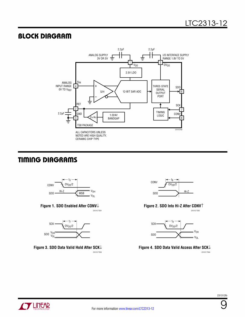
BLOCK DIAGRAM
231312 BD
4
–
+S/H
2.5V LDO
2×/4×1.024V
BANDGAP
TIMINGLOGIC
1
6
7
8
THREE-STATESERIALOUTPUT
PORT
12-BIT SAR ADC
2
3
AIN
REF
VDD OVDD
2.2µF GND
ANALOGINPUT RANGE
0V TO VREF
ANALOG SUPPLY3V OR 5V
I/O INTERFACE SUPPLYRANGE 1.8V TO 5V
5
2.2µF2.2µF
SDO
SCK
CONV
TS8 PACKAGE
ALL CAPACITORS UNLESSNOTED ARE HIGH QUALITY, CERAMIC CHIP TYPE
231312 TD04231312 TD03
231312 TD02231312 TD01
Hi-ZMSB
CONV OVDD/2
SDOVOH
t3
Hi-Z
CONVOVDD/2
SDO
t8
VOHVOL
SCKOVDD/2
SDO
t7
VOH
VOL
SCKOVDD/2
SDO
t4
Figure 1. SDO Enabled After CONV↓
Figure 3. SDO Data Valid Hold After SCK↓
Figure 2. SDO Into Hi-Z After CONV↑
Figure 4. SDO Data Valid Access After SCK↓
VOL
LTC2313-12
10231312fb
For more information www.linear.com/LTC2313-12
APPLICATIONS INFORMATIONOverview
The LTC2313-12 is a low noise, high speed, 12-bit succes-sive approximation register (SAR) ADC. The LTC2313-12 operates from a single 3V or 5V supply and provides a low drift (20ppm/°C maximum), internal reference and reference buffer. The internal reference buffer is automati-cally configured with a 2.048V span in low supply range (2.7V to 3.6V) and with a 4.096V span in the high supply range (4.75V to 5.25V). The LTC2313-12 samples up to a 2.5Msps rate and supports a 90MHz serial data read clock. The LTC2313-12 achieves excellent dynamic per-formance (72.6dB SINAD, –84dB THD) while dissipating only 25mW from a 5V supply at the 2.5Msps conversion rate. The LTC2313-12 outputs the conversion data with no cycle latency onto the SDO pin. The SDO pin output logic levels are supplied by the dedicated OVDD supply pin which has a wide supply range (1.71V to 5.25V) allowing the LTC2313-12 to communicate with 1.8V, 2.5V, 3V or 5V systems. The LTC2313-12 automatically switches to nap mode following the conversion process to save power. The device also provides a sleep power-down mode through serial interface control to reduce power dissipation during long inactive periods.
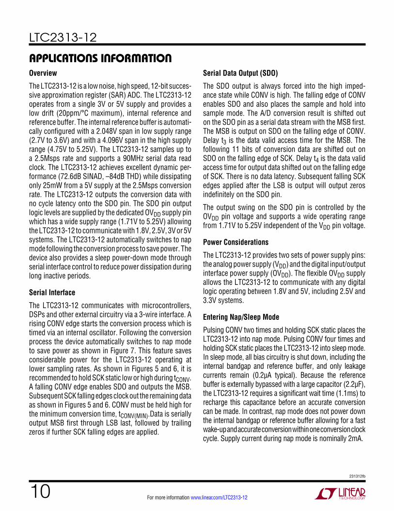
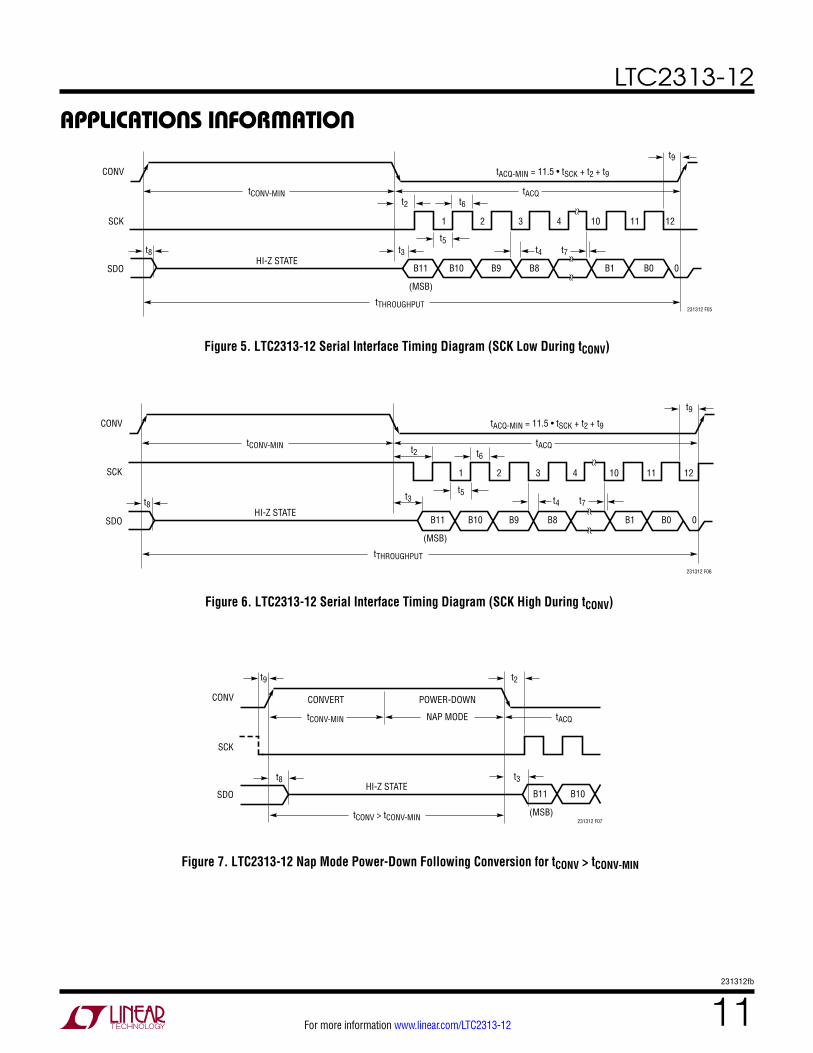
Serial Interface
The LTC2313-12 communicates with microcontrollers, DSPs and other external circuitry via a 3-wire interface. A rising CONV edge starts the conversion process which is timed via an internal oscillator. Following the conversion process the device automatically switches to nap mode to save power as shown in Figure 7. This feature saves considerable power for the LTC2313-12 operating at lower sampling rates. As shown in Figures 5 and 6, it is recommended to hold SCK static low or high during tCONV. A falling CONV edge enables SDO and outputs the MSB. Subsequent SCK falling edges clock out the remaining data as shown in Figures 5 and 6. CONV must be held high for the minimum conversion time, tCONV(MIN).Data is serially output MSB first through LSB last, followed by trailing zeros if further SCK falling edges are applied.
Serial Data Output (SDO)
The SDO output is always forced into the high imped-ance state while CONV is high. The falling edge of CONV enables SDO and also places the sample and hold into sample mode. The A/D conversion result is shifted out on the SDO pin as a serial data stream with the MSB first. The MSB is output on SDO on the falling edge of CONV. Delay t3 is the data valid access time for the MSB. The following 11 bits of conversion data are shifted out on SDO on the falling edge of SCK. Delay t4 is the data valid access time for output data shifted out on the falling edge of SCK. There is no data latency. Subsequent falling SCK edges applied after the LSB is output will output zeros indefinitely on the SDO pin.
The output swing on the SDO pin is controlled by the OVDD pin voltage and supports a wide operating range from 1.71V to 5.25V independent of the VDD pin voltage.
Power Considerations
The LTC2313-12 provides two sets of power supply pins: the analog power supply (VDD) and the digital input/output interface power supply (OVDD). The flexible OVDD supply allows the LTC2313-12 to communicate with any digital logic operating between 1.8V and 5V, including 2.5V and 3.3V systems.
Entering Nap/Sleep Mode
Pulsing CONV two times and holding SCK static places the LTC2313-12 into nap mode. Pulsing CONV four times and holding SCK static places the LTC2313-12 into sleep mode. In sleep mode, all bias circuitry is shut down, including the internal bandgap and reference buffer, and only leakage currents remain (0.2µA typical). Because the reference buffer is externally bypassed with a large capacitor (2.2µF), the LTC2313-12 requires a significant wait time (1.1ms) to recharge this capacitance before an accurate conversion can be made. In contrast, nap mode does not power down the internal bandgap or reference buffer allowing for a fast wake-up and accurate conversion within one conversion clock cycle. Supply current during nap mode is nominally 2mA.
LTC2313-12
11231312fb
For more information www.linear.com/LTC2313-12
Figure 6. LTC2313-12 Serial Interface Timing Diagram (SCK High During tCONV)
Figure 7. LTC2313-12 Nap Mode Power-Down Following Conversion for tCONV > tCONV-MIN
APPLICATIONS INFORMATION
Figure 5. LTC2313-12 Serial Interface Timing Diagram (SCK Low During tCONV)
tTHROUGHPUT
tACQtCONV-MIN
tACQ-MIN = 11.5 • tSCK + t2 + t9
1211104321
CONV
SCK
SDOHI-Z STATE
231312 F05
t6t2
(MSB)
B1 B0 0B8B9B10B11
t5t4 t7t3t8
t9
tTHROUGHPUT
tACQtCONV-MIN
tACQ-MIN = 11.5 • tSCK + t2 + t9
1211104321
CONV
SCK
SDOHI-Z STATE
231312 F06
t6t2
(MSB)
B1 B0 0B8B9B10B11
t5t3t8
t9
t4 t7
tCONV > tCONV-MIN
tACQtCONV-MIN NAP MODE
CONV
SCK
SDOHI-Z STATE
CONVERT POWER-DOWN
231312 F07(MSB)
B10B11
t3
t9 t2
t8
LTC2313-12
12231312fb
For more information www.linear.com/LTC2313-12
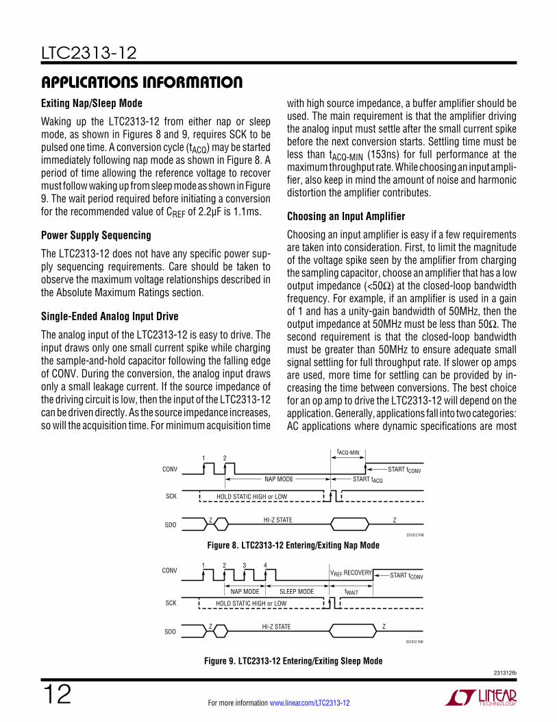
APPLICATIONS INFORMATIONExiting Nap/Sleep Mode
Waking up the LTC2313-12 from either nap or sleep mode, as shown in Figures 8 and 9, requires SCK to be pulsed one time. A conversion cycle (tACQ) may be started immediately following nap mode as shown in Figure 8. A period of time allowing the reference voltage to recover must follow waking up from sleep mode as shown in Figure 9. The wait period required before initiating a conversion for the recommended value of CREF of 2.2µF is 1.1ms.
Power Supply Sequencing
The LTC2313-12 does not have any specific power sup-ply sequencing requirements. Care should be taken to observe the maximum voltage relationships described in the Absolute Maximum Ratings section.
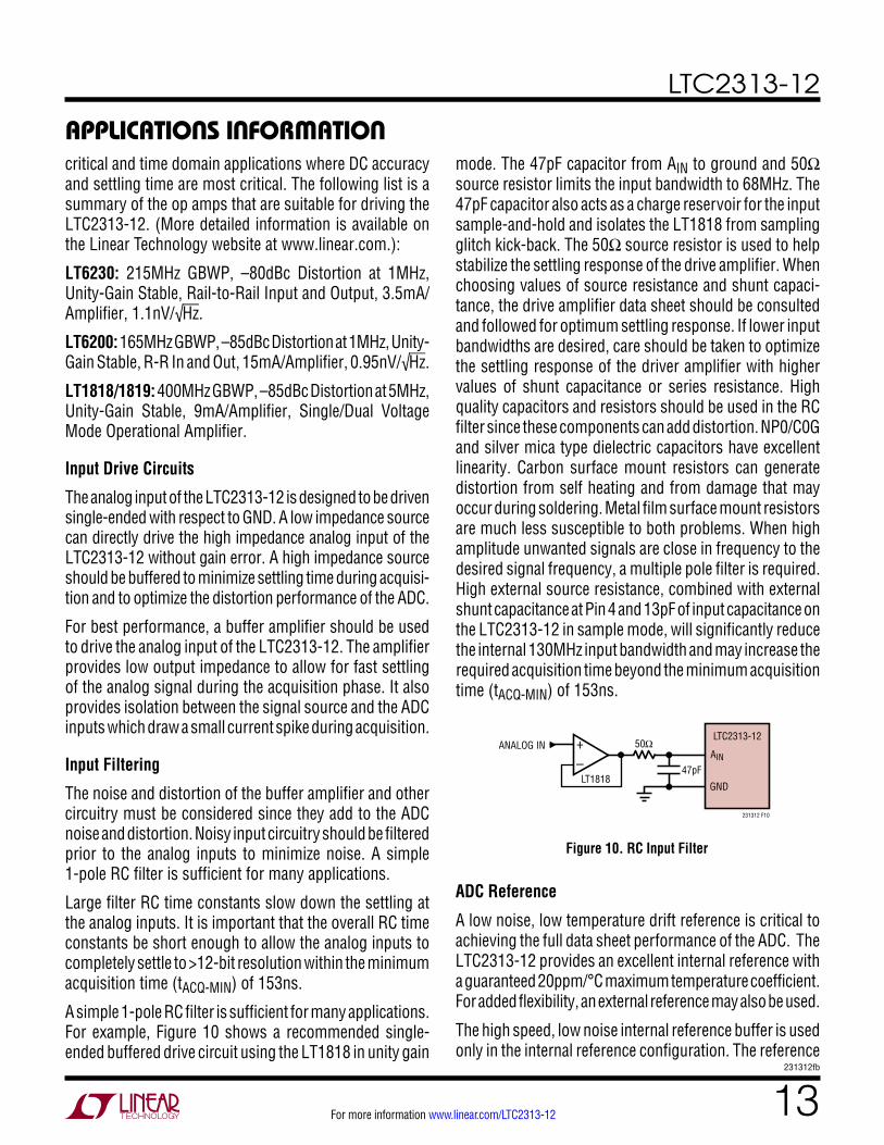
Single-Ended Analog Input Drive
The analog input of the LTC2313-12 is easy to drive. The input draws only one small current spike while charging the sample-and-hold capacitor following the falling edge of CONV. During the conversion, the analog input draws only a small leakage current. If the source impedance of the driving circuit is low, then the input of the LTC2313-12 can be driven directly. As the source impedance increases, so will the acquisition time. For minimum acquisition time
Figure 8. LTC2313-12 Entering/Exiting Nap Mode
Figure 9. LTC2313-12 Entering/Exiting Sleep Mode
with high source impedance, a buffer amplifier should be used. The main requirement is that the amplifier driving the analog input must settle after the small current spike before the next conversion starts. Settling time must be less than tACQ-MIN (153ns) for full performance at the maximum throughput rate. While choosing an input ampli-fier, also keep in mind the amount of noise and harmonic distortion the amplifier contributes.
Choosing an Input Amplifier
Choosing an input amplifier is easy if a few requirements are taken into consideration. First, to limit the magnitude of the voltage spike seen by the amplifier from charging the sampling capacitor, choose an amplifier that has a low output impedance (<50Ω) at the closed-loop bandwidth frequency. For example, if an amplifier is used in a gain of 1 and has a unity-gain bandwidth of 50MHz, then the output impedance at 50MHz must be less than 50Ω. The second requirement is that the closed-loop bandwidth must be greater than 50MHz to ensure adequate small signal settling for full throughput rate. If slower op amps are used, more time for settling can be provided by in-creasing the time between conversions. The best choice for an op amp to drive the LTC2313-12 will depend on the application. Generally, applications fall into two categories: AC applications where dynamic specifications are most
CONV
SCK
1 2
Z ZSDO
HI-Z STATE
231312 F08
NAP MODE
HOLD STATIC HIGH or LOW
START tACQ
tACQ-MIN
START tCONV
CONV
SCK
1 2
Z Z
3 4
SDOHI-Z STATE
231312 F09
NAP MODE SLEEP MODE
HOLD STATIC HIGH or LOW
START tCONVVREF RECOVERY
tWAIT
LTC2313-12
13231312fb
For more information www.linear.com/LTC2313-12
APPLICATIONS INFORMATIONcritical and time domain applications where DC accuracy and settling time are most critical. The following list is a summary of the op amps that are suitable for driving the LTC2313-12. (More detailed information is available on the Linear Technology website at www.linear.com.):
LT6230: 215MHz GBWP, –80dBc Distortion at 1MHz, Unity-Gain Stable, Rail-to-Rail Input and Output, 3.5mA/Amplifier, 1.1nV/√Hz.
LT6200: 165MHz GBWP, –85dBc Distortion at 1MHz, Unity-Gain Stable, R-R In and Out, 15mA/Amplifier, 0.95nV/√Hz.
LT1818/1819: 400MHz GBWP, –85dBc Distortion at 5MHz, Unity-Gain Stable, 9mA/Amplifier, Single/Dual Voltage Mode Operational Amplifier.
Input Drive Circuits
The analog input of the LTC2313-12 is designed to be driven single-ended with respect to GND. A low impedance source can directly drive the high impedance analog input of the LTC2313-12 without gain error. A high impedance source should be buffered to minimize settling time during acquisi-tion and to optimize the distortion performance of the ADC.
For best performance, a buffer amplifier should be used to drive the analog input of the LTC2313-12. The amplifier provides low output impedance to allow for fast settling of the analog signal during the acquisition phase. It also provides isolation between the signal source and the ADC inputs which draw a small current spike during acquisition.
Input Filtering
The noise and distortion of the buffer amplifier and other circuitry must be considered since they add to the ADC noise and distortion. Noisy input circuitry should be filtered prior to the analog inputs to minimize noise. A simple 1-pole RC filter is sufficient for many applications.
Large filter RC time constants slow down the settling at the analog inputs. It is important that the overall RC time constants be short enough to allow the analog inputs to completely settle to >12-bit resolution within the minimum acquisition time (tACQ-MIN) of 153ns.
A simple 1-pole RC filter is sufficient for many applications. For example, Figure 10 shows a recommended single-ended buffered drive circuit using the LT1818 in unity gain
mode. The 47pF capacitor from AIN to ground and 50Ω source resistor limits the input bandwidth to 68MHz. The 47pF capacitor also acts as a charge reservoir for the input sample-and-hold and isolates the LT1818 from sampling glitch kick-back. The 50Ω source resistor is used to help stabilize the settling response of the drive amplifier. When choosing values of source resistance and shunt capaci-tance, the drive amplifier data sheet should be consulted and followed for optimum settling response. If lower input bandwidths are desired, care should be taken to optimize the settling response of the driver amplifier with higher values of shunt capacitance or series resistance. High quality capacitors and resistors should be used in the RC filter since these components can add distortion. NP0/C0G and silver mica type dielectric capacitors have excellent linearity. Carbon surface mount resistors can generate distortion from self heating and from damage that may occur during soldering. Metal film surface mount resistors are much less susceptible to both problems. When high amplitude unwanted signals are close in frequency to the desired signal frequency, a multiple pole filter is required. High external source resistance, combined with external shunt capacitance at Pin 4 and 13pF of input capacitance on the LTC2313-12 in sample mode, will significantly reduce the internal 130MHz input bandwidth and may increase the required acquisition time beyond the minimum acquisition time (tACQ-MIN) of 153ns.
Figure 10. RC Input Filter
47pF
50Ω
231312 F10
AIN
LTC2313-12
LT1818GND
ANALOG IN +–
ADC Reference
A low noise, low temperature drift reference is critical to achieving the full data sheet performance of the ADC. The LTC2313-12 provides an excellent internal reference with a guaranteed 20ppm/°C maximum temperature coefficient. For added flexibility, an external reference may also be used.
The high speed, low noise internal reference buffer is used only in the internal reference configuration. The reference
LTC2313-12
14231312fb
For more information www.linear.com/LTC2313-12
APPLICATIONS INFORMATIONbuffer must be overdriven in the external reference con-figuration with a voltage 50mV higher than the nominal reference output voltage in the internal configuration.
Using the Internal Reference
The internal bandgap and reference buffer are active by default when the LTC2313-12 is not in sleep mode. The reference voltage at the REF pin scales automatically with the supply voltage at the VDD pin. The scaling of the refer-ence voltage with supply is shown in Table 2. Table 2. Reference Voltage vs Supply Range
SUPPLY VOLTAGE (VDD) REF VOLTAGE (VREF)
2.7V < VDD < 3.6V 2.048V
4.75V < VDD < 5.25V 4.096V
The reference voltage also determines the full-scale analog input range of the LTC2313-12. For example, a 2.048V reference voltage will accommodate an analog input range from 0V to 2.048V. An analog input voltage that goes below 0V will be coded as all zeros and an analog input voltage that exceeds 2.048V will be coded as all ones.
It is recommended that the REF pin be bypassed to ground with a low ESR, 2.2µF ceramic chip capacitor for optimum performance.
External Reference
An external reference can be used with the LTC2313-12 if better performance is required or to accommodate a larger input voltage span. The only constraints are that the external reference voltage must be 50mV higher than
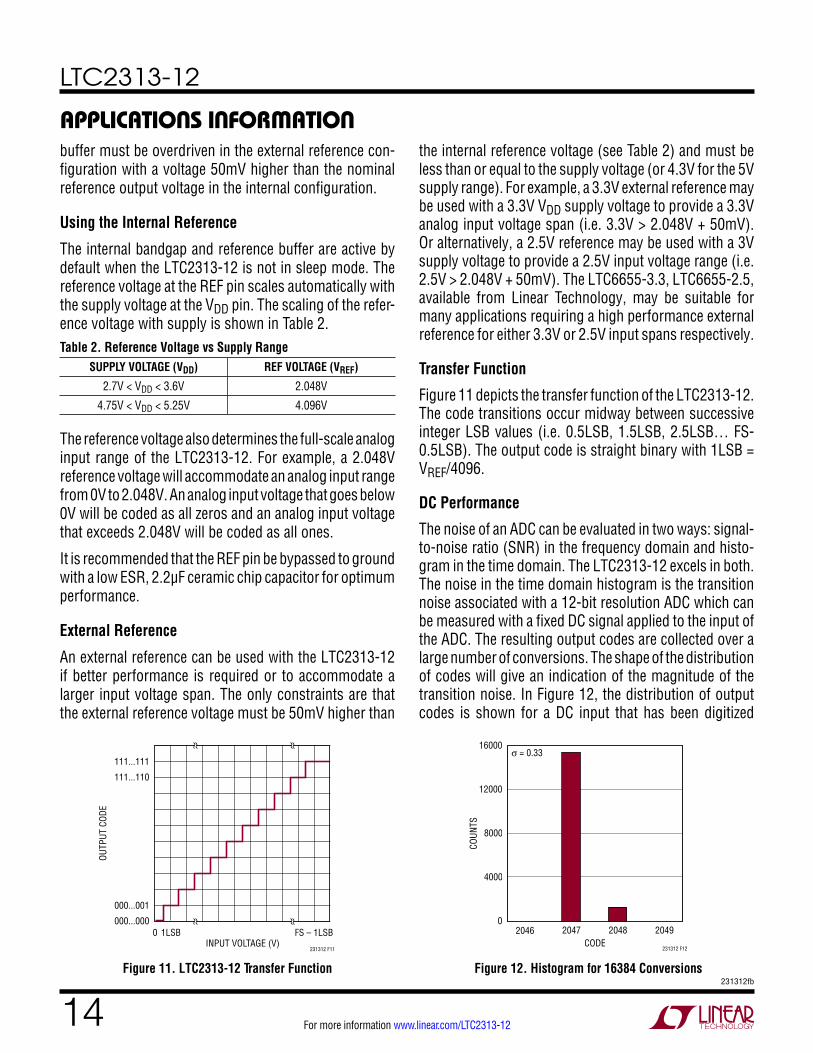
Figure 11. LTC2313-12 Transfer Function Figure 12. Histogram for 16384 Conversions
the internal reference voltage (see Table 2) and must be less than or equal to the supply voltage (or 4.3V for the 5V supply range). For example, a 3.3V external reference may be used with a 3.3V VDD supply voltage to provide a 3.3V analog input voltage span (i.e. 3.3V > 2.048V + 50mV). Or alternatively, a 2.5V reference may be used with a 3V supply voltage to provide a 2.5V input voltage range (i.e. 2.5V > 2.048V + 50mV). The LTC6655-3.3, LTC6655-2.5, available from Linear Technology, may be suitable for many applications requiring a high performance external reference for either 3.3V or 2.5V input spans respectively.
Transfer Function
Figure 11 depicts the transfer function of the LTC2313-12. The code transitions occur midway between successive integer LSB values (i.e. 0.5LSB, 1.5LSB, 2.5LSB… FS-0.5LSB). The output code is straight binary with 1LSB = VREF/4096.
DC Performance
The noise of an ADC can be evaluated in two ways: signal-to-noise ratio (SNR) in the frequency domain and histo-gram in the time domain. The LTC2313-12 excels in both. The noise in the time domain histogram is the transition noise associated with a 12-bit resolution ADC which can be measured with a fixed DC signal applied to the input of the ADC. The resulting output codes are collected over a large number of conversions. The shape of the distribution of codes will give an indication of the magnitude of the transition noise. In Figure 12, the distribution of output codes is shown for a DC input that has been digitized
INPUT VOLTAGE (V)
OUTP
UT C
ODE
231312 F11
111...111
111...110
000...000
000...001
FS – 1LSB0 1LSBCODE
COUN
TS
2047 2048
231312 F12
2046 2049
σ = 0.33
0
4000
8000
16000
12000
LTC2313-12
15231312fb
For more information www.linear.com/LTC2313-12
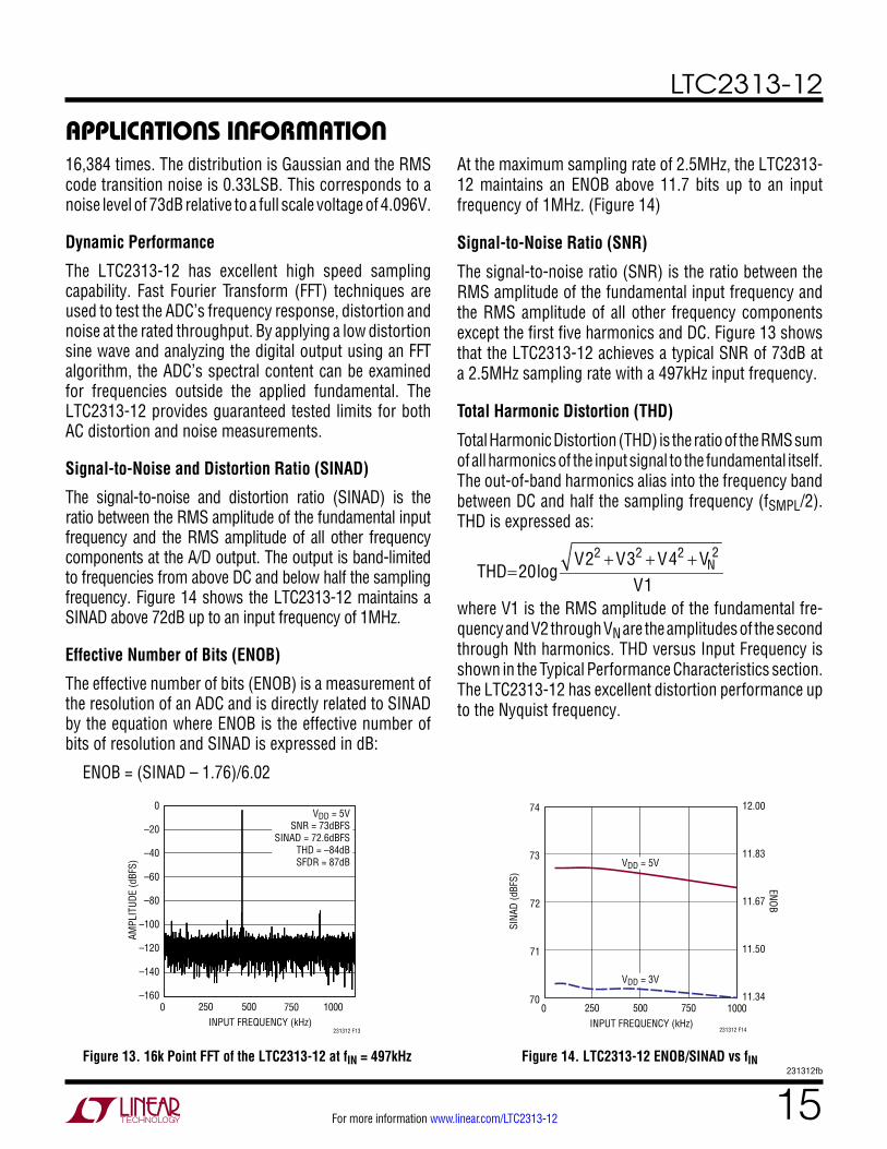
APPLICATIONS INFORMATIONAt the maximum sampling rate of 2.5MHz, the LTC2313-12 maintains an ENOB above 11.7 bits up to an input frequency of 1MHz. (Figure 14)
Signal-to-Noise Ratio (SNR)
The signal-to-noise ratio (SNR) is the ratio between the RMS amplitude of the fundamental input frequency and the RMS amplitude of all other frequency components except the first five harmonics and DC. Figure 13 shows that the LTC2313-12 achieves a typical SNR of 73dB at a 2.5MHz sampling rate with a 497kHz input frequency.
Total Harmonic Distortion (THD)
Total Harmonic Distortion (THD) is the ratio of the RMS sum of all harmonics of the input signal to the fundamental itself. The out-of-band harmonics alias into the frequency band between DC and half the sampling frequency (fSMPL/2). THD is expressed as:
THD=20log
V22 +V32 +V42 +VN2
V1where V1 is the RMS amplitude of the fundamental fre-quency and V2 through VN are the amplitudes of the second through Nth harmonics. THD versus Input Frequency is shown in the Typical Performance Characteristics section. The LTC2313-12 has excellent distortion performance up to the Nyquist frequency.
16,384 times. The distribution is Gaussian and the RMS code transition noise is 0.33LSB. This corresponds to a noise level of 73dB relative to a full scale voltage of 4.096V.
Dynamic Performance
The LTC2313-12 has excellent high speed sampling capability. Fast Fourier Transform (FFT) techniques are used to test the ADC’s frequency response, distortion and noise at the rated throughput. By applying a low distortion sine wave and analyzing the digital output using an FFT algorithm, the ADC’s spectral content can be examined for frequencies outside the applied fundamental. The LTC2313-12 provides guaranteed tested limits for both AC distortion and noise measurements.
Signal-to-Noise and Distortion Ratio (SINAD)
The signal-to-noise and distortion ratio (SINAD) is the ratio between the RMS amplitude of the fundamental input frequency and the RMS amplitude of all other frequency components at the A/D output. The output is band-limited to frequencies from above DC and below half the sampling frequency. Figure 14 shows the LTC2313-12 maintains a SINAD above 72dB up to an input frequency of 1MHz.
Effective Number of Bits (ENOB)
The effective number of bits (ENOB) is a measurement of the resolution of an ADC and is directly related to SINAD by the equation where ENOB is the effective number of bits of resolution and SINAD is expressed in dB:
ENOB = (SINAD – 1.76)/6.02
Figure 13. 16k Point FFT of the LTC2313-12 at fIN = 497kHz Figure 14. LTC2313-12 ENOB/SINAD vs fIN
231312 F13INPUT FREQUENCY (kHz)
AMPL
ITUD
E (d
BFS)
0 1000500250 750
0
–20
–40
–60
–80
–100
–120
–140
–160
VDD = 5VSNR = 73dBFS
SINAD = 72.6dBFSTHD = –84dBSFDR = 87dB
70
71
72
74
73
231312 F14INPUT FREQUENCY (kHz)
SINA
D (d
BFS)
ENOB
0 1000750500250
12.00
11.83
11.67
11.50
11.34
VDD = 5V
VDD = 3V
LTC2313-12
16231312fb
For more information www.linear.com/LTC2313-12
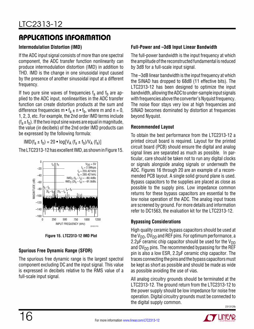
APPLICATIONS INFORMATIONIntermodulation Distortion (IMD)
If the ADC input signal consists of more than one spectral component, the ADC transfer function nonlinearity can produce intermodulation distortion (IMD) in addition to THD. IMD is the change in one sinusoidal input caused by the presence of another sinusoidal input at a different frequency.
If two pure sine waves of frequencies fa and fb are ap-plied to the ADC input, nonlinearities in the ADC transfer function can create distortion products at the sum and difference frequencies m • fa ± n • fb, where m and n = 0, 1, 2, 3, etc. For example, the 2nd order IMD terms include (fa ± fb). If the two input sine waves are equal in magnitude, the value (in decibels) of the 2nd order IMD products can be expressed by the following formula:
IMD(fa ± fb) = 20 • log[VA (fa ± fb)/VA (fa)]
The LTC2313-12 has excellent IMD, as shown in Figure 15.
Figure 15. LTC2313-12 IMD Plot
231312 F15INPUT FREQUENCY (kHz)
MAG
NITU
DE (d
B)
0 1250500250 750 1000
0
–20fa fb
2fa – fb 2fb – fa
fb – fa
–40
–60
–80
–100
–120
–140
–160
VDD = 5Vfs = 2.5Msps
fa = 255.421kHzfb = 285.421kHz
IMD2 (fb – fa) = –80.4dBcIMD3 (2fb – fa) = –91.8dBc
fa + fb
Full-Power and –3dB Input Linear Bandwidth
The full-power bandwidth is the input frequency at which the amplitude of the reconstructed fundamental is reduced by 3dB for a full-scale input signal.
The –3dB linear bandwidth is the input frequency at which the SINAD has dropped to 68dB (11 effective bits). The LTC2313-12 has been designed to optimize the input bandwidth, allowing the ADC to under-sample input signals with frequencies above the converter’s Nyquist frequency. The noise floor stays very low at high frequencies and SINAD becomes dominated by distortion at frequencies beyond Nyquist.
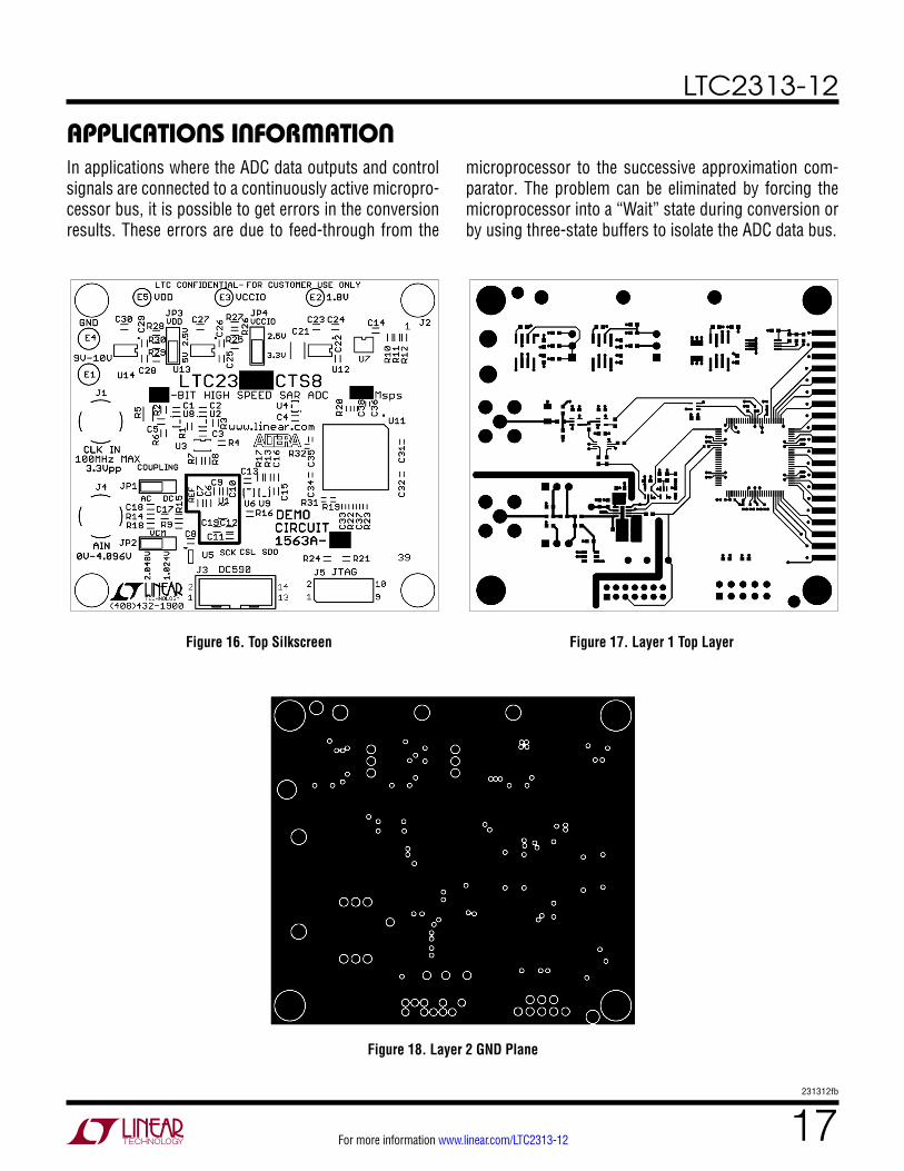
Recommended Layout
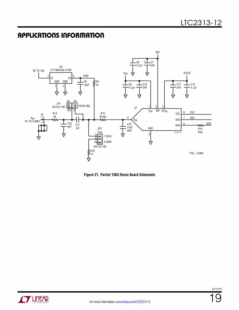
To obtain the best performance from the LTC2313-12 a printed circuit board is required. Layout for the printed circuit board (PCB) should ensure the digital and analog signal lines are separated as much as possible. In par-ticular, care should be taken not to run any digital clocks or signals alongside analog signals or underneath the ADC. Figures 16 through 20 are an example of a recom-mended PCB layout. A single solid ground plane is used. Bypass capacitors to the supplies are placed as close as possible to the supply pins. Low impedance common returns for these bypass capacitors are essential to the low noise operation of the ADC. The analog input traces are screened by ground. For more details and information refer to DC1563, the evaluation kit for the LTC2313-12.
Bypassing Considerations
High quality ceramic bypass capacitors should be used at the VDD, OVDD and REF pins. For optimum performance, a 2.2µF ceramic chip capacitor should be used for the VDD and OVDD pins. The recommended bypassing for the REF pin is also a low ESR, 2.2µF ceramic chip capacitor. The traces connecting the pins and the bypass capacitors must be kept as short as possible and should be made as wide as possible avoiding the use of vias.
All analog circuitry grounds should be terminated at the LTC2313-12. The ground return from the LTC2313-12 to the power supply should be low impedance for noise free operation. Digital circuitry grounds must be connected to the digital supply common.
Spurious Free Dynamic Range (SFDR)
The spurious free dynamic range is the largest spectral component excluding DC and the input signal. This value is expressed in decibels relative to the RMS value of a full-scale input signal.
LTC2313-12
17231312fb
For more information www.linear.com/LTC2313-12
APPLICATIONS INFORMATION
Figure 16. Top Silkscreen Figure 17. Layer 1 Top Layer
Figure 18. Layer 2 GND Plane
In applications where the ADC data outputs and control signals are connected to a continuously active micropro-cessor bus, it is possible to get errors in the conversion results. These errors are due to feed-through from the
microprocessor to the successive approximation com-parator. The problem can be eliminated by forcing the microprocessor into a “Wait” state during conversion or by using three-state buffers to isolate the ADC data bus.
LTC2313-12
18231312fb
For more information www.linear.com/LTC2313-12
Figure 19. Layer 3 PWR Plane
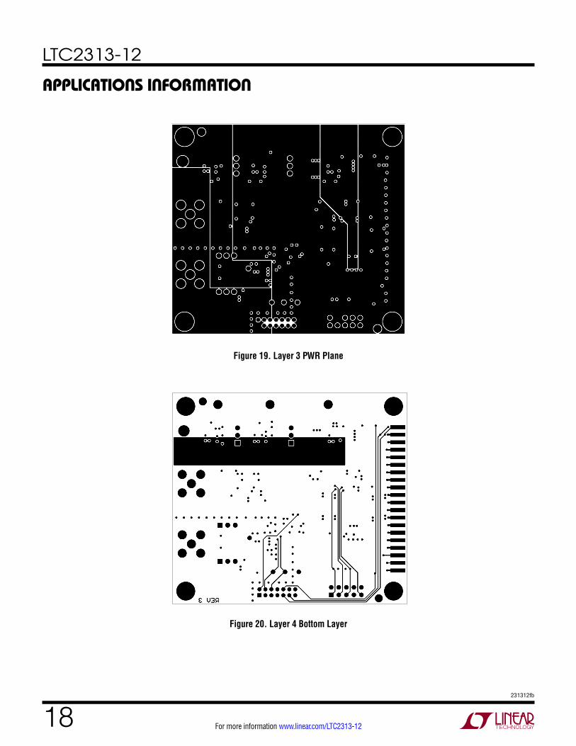
Figure 20. Layer 4 Bottom Layer
APPLICATIONS INFORMATION
LTC2313-12
19231312fb
For more information www.linear.com/LTC2313-12
Figure 21. Partial 1563 Demo Board Schematic
APPLICATIONS INFORMATION
4
9V TO 10VU5
LT1790ACS6-2.048
1
1
AC
J4
DC
COUPLING2 3
2
6
GND
GND
VDD REFCSL
SCK
CSL*
SCK
SDO SDO
OVDD
VI VOVCM
VDD VCCIO
C810µF C9
4.7µFC10OPT
C11OPT
C124.7µF
C7OPT
REF
+C64.7µF
R91k
C18OPT
R181k
31.024V
2.048V
HD1X3-100
21
C171µF JP2
VCM
R140k
R1549.9Ω
R1633Ω
4
3231312 F21
1 2 5
8
7
6
U1*
C1947pFNP0
JP1HD1X3-100
AIN0V TO 4.096V AIN
GND
*CSL = CONV
LTC2313-12
20231312fb
For more information www.linear.com/LTC2313-12
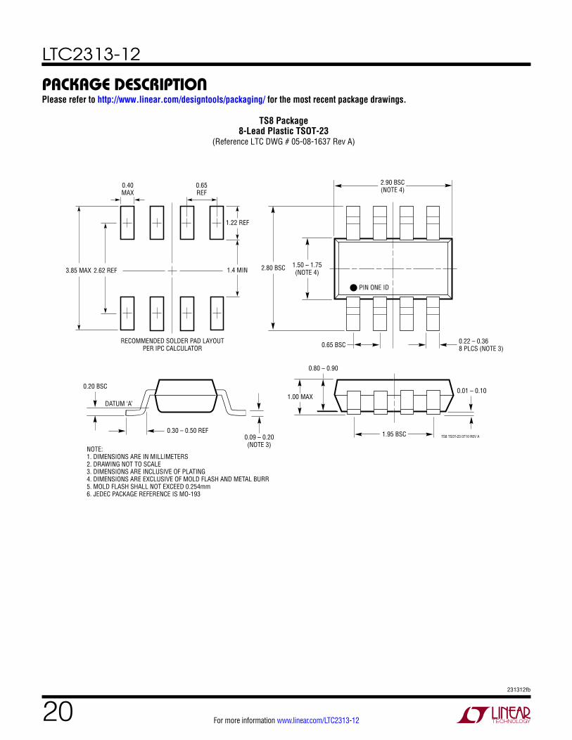
PACKAGE DESCRIPTIONPlease refer to http://www.linear.com/designtools/packaging/ for the most recent package drawings.
1.50 – 1.75(NOTE 4)
2.80 BSC
0.22 – 0.36 8 PLCS (NOTE 3)
DATUM ‘A’
0.09 – 0.20(NOTE 3)
TS8 TSOT-23 0710 REV A
2.90 BSC(NOTE 4)
0.65 BSC
1.95 BSC
0.80 – 0.90
1.00 MAX0.01 – 0.10
0.20 BSC
0.30 – 0.50 REF
PIN ONE ID
NOTE:1. DIMENSIONS ARE IN MILLIMETERS2. DRAWING NOT TO SCALE3. DIMENSIONS ARE INCLUSIVE OF PLATING4. DIMENSIONS ARE EXCLUSIVE OF MOLD FLASH AND METAL BURR5. MOLD FLASH SHALL NOT EXCEED 0.254mm6. JEDEC PACKAGE REFERENCE IS MO-193
3.85 MAX
0.40MAX
0.65REF
RECOMMENDED SOLDER PAD LAYOUTPER IPC CALCULATOR
1.4 MIN2.62 REF
1.22 REF
TS8 Package8-Lead Plastic TSOT-23
(Reference LTC DWG # 05-08-1637 Rev A)
LTC2313-12
21231312fb
For more information www.linear.com/LTC2313-12
Information furnished by Linear Technology Corporation is believed to be accurate and reliable. However, no responsibility is assumed for its use. Linear Technology Corporation makes no representa-tion that the interconnection of its circuits as described herein will not infringe on existing patent rights.
REVISION HISTORYREV DATE DESCRIPTION PAGE NUMBER
A 11/13 Added pin-compatible family table 1
Reordered/renumbered notes 3, 5
B 01/15 Updated Timing Diagrams (Figures 8 and 9) 12
LTC2313-12
22231312fb
For more information www.linear.com/LTC2313-12 LINEAR TECHNOLOGY CORPORATION 2013
LT 0115 REV B • PRINTED IN USALinear Technology Corporation1630 McCarthy Blvd., Milpitas, CA 95035-7417(408) 432-1900 ● FAX: (408) 434-0507 ● www.linear.com/LTC2313-12
RELATED PARTS
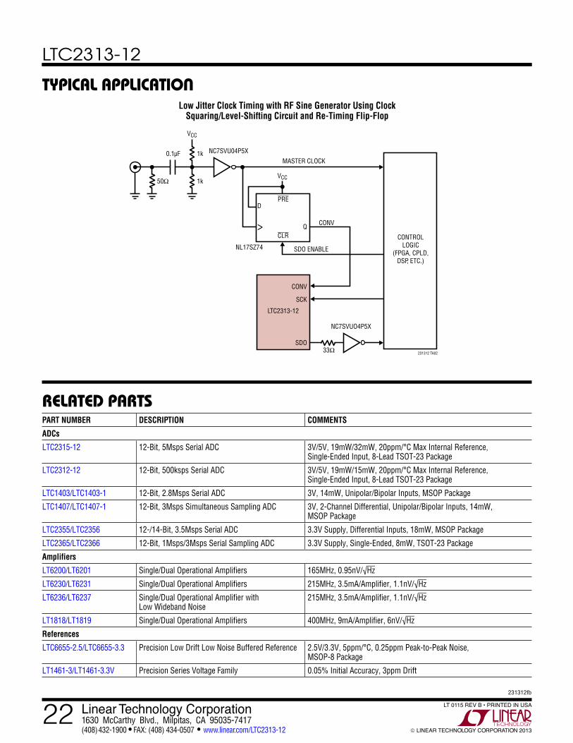
TYPICAL APPLICATIONLow Jitter Clock Timing with RF Sine Generator Using Clock
Squaring/Level-Shifting Circuit and Re-Timing Flip-Flop
PART NUMBER DESCRIPTION COMMENTS
ADCs
LTC2315-12 12-Bit, 5Msps Serial ADC 3V/5V, 19mW/32mW, 20ppm/°C Max Internal Reference, Single-Ended Input, 8-Lead TSOT-23 Package
LTC2312-12 12-Bit, 500ksps Serial ADC 3V/5V, 19mW/15mW, 20ppm/°C Max Internal Reference, Single-Ended Input, 8-Lead TSOT-23 Package
LTC1403/LTC1403-1 12-Bit, 2.8Msps Serial ADC 3V, 14mW, Unipolar/Bipolar Inputs, MSOP Package
LTC1407/LTC1407-1 12-Bit, 3Msps Simultaneous Sampling ADC 3V, 2-Channel Differential, Unipolar/Bipolar Inputs, 14mW, MSOP Package
LTC2355/LTC2356 12-/14-Bit, 3.5Msps Serial ADC 3.3V Supply, Differential Inputs, 18mW, MSOP Package
LTC2365/LTC2366 12-Bit, 1Msps/3Msps Serial Sampling ADC 3.3V Supply, Single-Ended, 8mW, TSOT-23 Package
Amplifiers
LT6200/LT6201 Single/Dual Operational Amplifiers 165MHz, 0.95nV/√Hz
LT6230/LT6231 Single/Dual Operational Amplifiers 215MHz, 3.5mA/Amplifier, 1.1nV/√Hz
LT6236/LT6237 Single/Dual Operational Amplifier with Low Wideband Noise
215MHz, 3.5mA/Amplifier, 1.1nV/√Hz
LT1818/LT1819 Single/Dual Operational Amplifiers 400MHz, 9mA/Amplifier, 6nV/√Hz
References
LTC6655-2.5/LTC6655-3.3 Precision Low Drift Low Noise Buffered Reference 2.5V/3.3V, 5ppm/°C, 0.25ppm Peak-to-Peak Noise, MSOP-8 Package
LT1461-3/LT1461-3.3V Precision Series Voltage Family 0.05% Initial Accuracy, 3ppm Drift
CONTROLLOGIC
(FPGA, CPLD,DSP, ETC.)
50Ω
1k
1k
0.1µF
VCC
VCC
NC7SVU04P5X
NL17SZ74
NC7SVUO4P5X
MASTER CLOCK
SDO ENABLE
DPRE
CLR
CONVQ
CONV
SCK
SDO
>
LTC2313-12
33Ω 231312 TA02


![ADC-20 und ADC-24 › download › datasheets › adc20...Datenlogger ADC-20 und ADC-24 ADC-20 ADC-24 Auflösung 20 Bit 24 Bit Anzahl Kanäle[1] 4 differenzial / 8 einpolig 8 differenzial](https://img.pdfslide.net/doc/110x75/5f23cbdc98bf2e58da663aad/adc-20-und-adc-24-a-download-a-datasheets-a-adc20-datenlogger-adc-20-und.jpg)