Embed Size (px)
Citation preview
LTC3553
13553fc
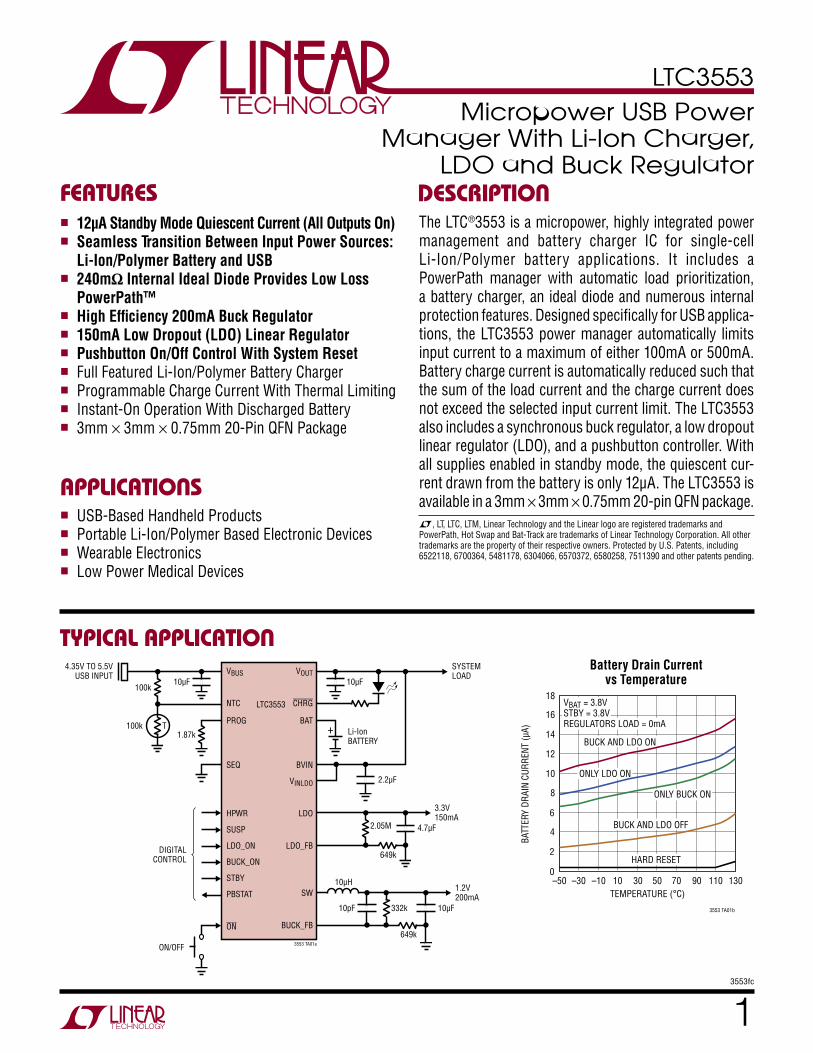
Typical applicaTion
DescripTion
Micropower USB Power Manager With Li-Ion Charger,
LDO and Buck Regulator
The LTC®3553 is a micropower, highly integrated power management and battery charger IC for single-cell Li-Ion/Polymer battery applications. It includes a PowerPath manager with automatic load prioritization, a battery charger, an ideal diode and numerous internal protection features. Designed specifically for USB applica-tions, the LTC3553 power manager automatically limits input current to a maximum of either 100mA or 500mA. Battery charge current is automatically reduced such that the sum of the load current and the charge current does not exceed the selected input current limit. The LTC3553 also includes a synchronous buck regulator, a low dropout linear regulator (LDO), and a pushbutton controller. With all supplies enabled in standby mode, the quiescent cur-rent drawn from the battery is only 12μA. The LTC3553 is available in a 3mm × 3mm × 0.75mm 20-pin QFN package.
Battery Drain Current vs Temperature
FeaTures
applicaTions
n 12μA Standby Mode Quiescent Current (All Outputs On)n Seamless Transition Between Input Power Sources:
Li-Ion/Polymer Battery and USBn 240mΩ Internal Ideal Diode Provides Low Loss
PowerPath™n High Efficiency 200mA Buck Regulatorn 150mA Low Dropout (LDO) Linear Regulatorn Pushbutton On/Off Control With System Resetn Full Featured Li-Ion/Polymer Battery Chargern Programmable Charge Current With Thermal Limitingn Instant-On Operation With Discharged Batteryn 3mm × 3mm × 0.75mm 20-Pin QFN Package
n USB-Based Handheld Productsn Portable Li-Ion/Polymer Based Electronic Devicesn Wearable Electronicsn Low Power Medical Devices
VBUS
NTC
PROG
SEQ
HPWR
SUSP
LDO_ON
BUCK_ON
STBY
PBSTAT
ON
VOUT
CHRG
BAT
BVIN
VINLDO
LDO
LDO_FB
SW
BUCK_FB
ON/OFF
Li-IonBATTERY
10µF
2.2µF
10µF100k
100k
DIGITALCONTROL
T1.87k
4.7µF2.05M
649k
3.3V150mA
10pF 10µF332k
649k
1.2V200mA
3553 TA01a
10µH
SYSTEMLOAD
4.35V TO 5.5VUSB INPUT
LTC3553
+
TEMPERATURE (°C)–50 –30 –10 30 50 70 90 13011010
0
BATT
ERY
DRAI
N CU
RREN
T (µ
A)
4
6
10
18
16
14
12
8
3553 TA01b
2
BUCK AND LDO ON
VBAT = 3.8VSTBY = 3.8VREGULATORS LOAD = 0mA
ONLY LDO ON
ONLY BUCK ON
BUCK AND LDO OFF
HARD RESET
L, LT, LTC, LTM, Linear Technology and the Linear logo are registered trademarks and PowerPath, Hot Swap and Bat-Track are trademarks of Linear Technology Corporation. All other trademarks are the property of their respective owners. Protected by U.S. Patents, including 6522118, 6700364, 5481178, 6304066, 6570372, 6580258, 7511390 and other patents pending.

LTC3553
23553fc
pin conFiguraTionabsoluTe MaxiMuM raTings
VBUS, VOUT t < 1ms and Duty Cycle < 1% .................. –0.3V to 7V Steady State ............................................. –0.3V to 6VBAT, NTC, CHRG, SUSP, PBSTAT, ON, BUCK_FB, LDO_FB ................................ –0.3V to 6VBUCK_ON, LDO_ON, STBY, SEQ, HPWR,BVIN, VINLDO, LDO (Note 4) .............–0.3V to VCC + 0.3VIBAT .............................................................................1AISW (Continuous) .................................................300mAILDO (Continuous) ................................................175mAICHRG, IPBSTAT .........................................................75mAOperating Temperature Range.................. –40°C to 85°CJunction Temperature ........................................... 110°CStorage Temperature Range ................... –65°C to 125°C
(Notes 1, 2, 3)
orDer inForMaTionLEAD FREE FINISH TAPE AND REEL PART MARKING PACKAGE DESCRIPTION TEMPERATURE RANGE
LTC3553EUD#PBF LTC3553EUD#TRPBF LFYB 20-Lead (3mm × 3mm) Plastic QFN –40°C to 85°C
LTC3553EPD#PBF LTC3553EPD#TRPBF FHST 20-Lead (3mm × 3mm) Plastic UTQFN –40°C to 85°C (OBSOLETE)
Consult LTC Marketing for parts specified with wider operating temperature ranges. Consult LTC Marketing for information on non-standard lead based finish parts.For more information on lead free part marking, go to: http://www.linear.com/leadfree/ For more information on tape and reel specifications, go to: http://www.linear.com/tapeandreel/
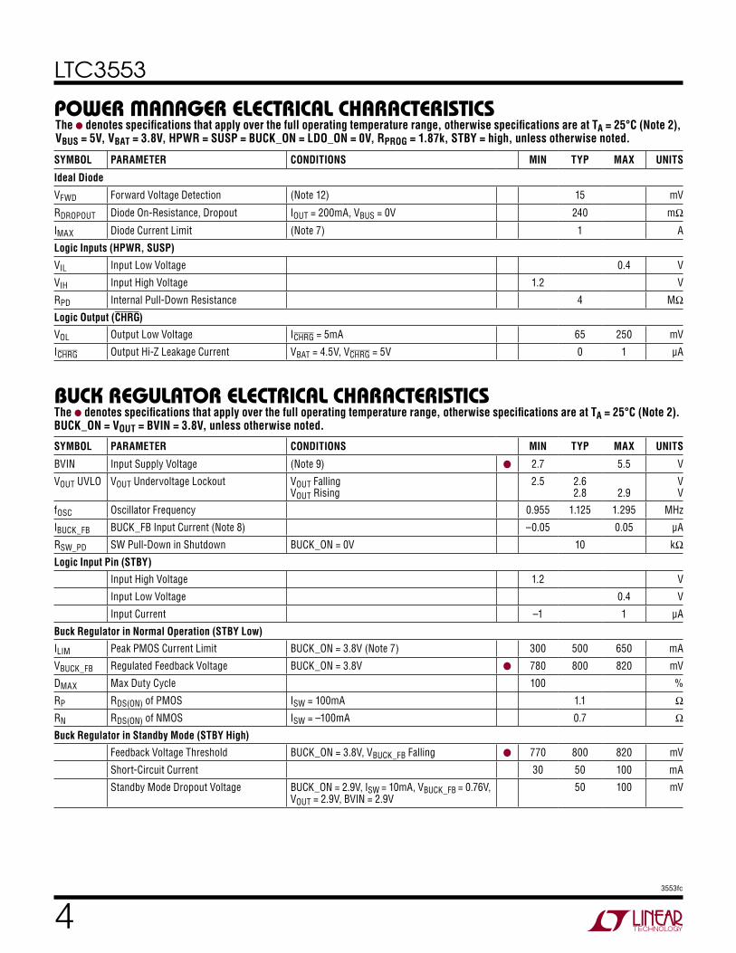
poWer Manager elecTrical characTerisTicsThe l denotes specifications that apply over the full operating temperature range, otherwise specifications are at TA = 25°C (Note 2), VBUS = 5V, VBAT = 3.8V, HPWR = SUSP = BUCK_ON = LDO_ON = 0V, RPROG = 1.87k, STBY = high, unless otherwise noted.
SYMBOL PARAMETER CONDITIONS MIN TYP MAX UNITS
No-Load Quiescent Currents
IBATQ Battery Drain Current (Note 5) Buck and LDO Shutdown, Hard Reset Buck and LDO Shutdown Buck and LDO Enabled, Standby Mode Buck and LDO Enabled Buck Enabled, LDO Shutdown LDO Enabled, Buck Shutdown
IOUT = ISW = ILDO = 0 VBUS = 0V, Hard Reset VBUS = 0V VBUS = 0V, BUCK_ON = LDO_ON = STBY = 3.8V VBUS = 0V, BUCK_ON = LDO_ON = 3.8V, STBY = 0V VBUS = 0V, BUCK_ON = 3.8V, LDO_ON = 0V STBY = 0V VBUS = 0V, LDO_ON = 3.8V, BUCK_ON = 0V, STBY = 0V
0.2 3 8 16
6.5
16
2 5 16 35
15
35
µA µA µA µA
µA
µA
IBATQC Battery Drain Current, VBUS Available VBAT = VFLOAT, Timer Timed Out 5 8 µA
IBUSQ VBUS Input Current 100mA, 500mA Modes Charger On Timer Timed Out SUSP = 5V (Suspend Mode)
300 150 15
500 350 30
µA µA µA
20 19 18 17 16
7 8
TOP VIEW
21GND
UD PACKAGE20-LEAD (3mm × 3mm) PLASTIC QFN
9 10
HPWR
SEQ
PBSTAT
ON
LDO_ON
NTC
CHRG
SW
BVIN
VINLDO
V BUS
SUSP
V OUT
BAT
PROG
STBY
BUCK
_ON
BUCK
_FB
LDO_
FB
LDO
12
11
13
14
15
4
5
3
2
1
6
TJMAX = 110°C, θJA = 58.7°C/WEXPOSED PAD (PIN 21) IS GND, AND MUST BE SOLDERED TO PCB GND
LTC3553
33553fc
poWer Manager elecTrical characTerisTics
SYMBOL PARAMETER CONDITIONS MIN TYP MAX UNITS
IBVINQ BVIN Input Current Buck Shutdown Buck Enabled, Standby Mode Buck Enabled
VBUS = 0V, VBVIN = 3.8V, ISW = 0 (Note 8) BUCK_ON = 0V BUCK_ON = STBY = 3.8V BUCK_ON = 3.8V, STBY = 0V
0.01 1.5 22
1 3
38
µA µA µA
IVINLDOQ VINLDO Input Current LDO Shutdown LDO Enabled, Standby Mode LDO Enabled
VBUS = 0V, VINLDO = 3.8V, ILDO = 0 (Note 10) LDO_ON = 0V LDO_ON = STBY = 3.8V LDO_ON = 3.8V, STBY = 0V
0.01 0.1 0.1
1 1 1
µA µA µA
Input Power Supply
VBUS Input Supply Voltage 4.35 5.5 V
IBUS(LIM) Total Input Current HPWR = 0V (100mA) HPWR = 5V (500mA)
l
l
80 400
90 450
100 500
mA mA
VUVLO VBUS Undervoltage Lockout Rising Threshold Falling Threshold
3.5
3.8 3.6
3.9 V mV
VDUVLO VBUS to BAT Differential Undervoltage Lockout
Rising Threshold Falling Threshold
0
200 50
300 mV mV
RON_ILIM Input Current Limit Power FET On-Resistance (Between VBUS and VOUT)
350 mΩ
Battery Charger
VFLOAT VBAT Regulated Output Voltage 0 ≤ TA ≤ 85°C
4.179 4.165
4.2 4.2
4.221 4.235
V V
ICHG Constant-Current Mode Charge Current RPROG = 1.87k, 0 ≤ TA ≤ 85°C 380 400 420 mA
VPROG VPROG,TRKL
PROG Pin Servo Voltage PROG Pin Servo Voltage in Trickle Charge
VBAT < VTRKL
1 0.1
V V
hPROG Ratio of IBAT to PROG Pin Current 750 mA/mA
ITRKL Trickle Charge Current VBAT < VTRKL 30 40 50 mA
VTRKL Trickle Charge Threshold Voltage VBAT Rising VBAT Falling
2.6
2.9 2.75
3 V V
ΔVRECHRG Recharge Battery Threshold Voltage Threshold Voltage Relative to VFLOAT –75 –100 –125 mV
tTERM Safety Timer Termination Period Timer Starts when VBAT = VFLOAT – 50mV 3.2 4 5 Hour
tBADBAT Bad Battery Termination Time VBAT < VTRKL 0.4 0.5 0.63 Hour
hC/10 End-of-Charge Indication Current Ratio (Note 6) 0.085 0.1 0.115 mA/mA
RON_CHG Battery Charger Power FET On-Resistance (Between VOUT and BAT)
IBAT = 200mA 220 mΩ
TLIM Junction Temperature in Constant Temperature Mode
110 °C
NTC
VCOLD Cold Temperature Fault Threshold Voltage
Rising NTC Voltage Hysteresis
75 76 1.3
77 %VBUS %VBUS
VHOT Hot Temperature Fault Threshold Voltage Falling NTC Voltage Hysteresis
34 35 1.3
36 %VBUS %VBUS
VDIS NTC Disable Threshold Voltage Falling NTC Voltage Hysteresis
l 1.2 1.7 50
2.2 %VBUS mV
INTC NTC Leakage Current VNTC = VBUS = 5V –50 50 nA
The l denotes specifications that apply over the full operating temperature range, otherwise specifications are at TA = 25°C (Note 2), VBUS = 5V, VBAT = 3.8V, HPWR = SUSP = BUCK_ON = LDO_ON = 0V, RPROG = 1.87k, STBY = high, unless otherwise noted.
LTC3553
43553fc
bucK regulaTor elecTrical characTerisTicsThe l denotes specifications that apply over the full operating temperature range, otherwise specifications are at TA = 25°C (Note 2). BUCK_ON = VOUT = BVIN = 3.8V, unless otherwise noted.
SYMBOL PARAMETER CONDITIONS MIN TYP MAX UNITS
BVIN Input Supply Voltage (Note 9) l 2.7 5.5 V
VOUT UVLO VOUT Undervoltage Lockout VOUT Falling VOUT Rising
2.5 2.6 2.8
2.9
V V
fOSC Oscillator Frequency 0.955 1.125 1.295 MHz
IBUCK_FB BUCK_FB Input Current (Note 8) –0.05 0.05 µA
RSW_PD SW Pull-Down in Shutdown BUCK_ON = 0V 10 kΩ
Logic Input Pin (STBY)
Input High Voltage 1.2 V
Input Low Voltage 0.4 V
Input Current –1 1 µA
Buck Regulator in Normal Operation (STBY Low)
ILIM Peak PMOS Current Limit BUCK_ON = 3.8V (Note 7) 300 500 650 mA
VBUCK_FB Regulated Feedback Voltage BUCK_ON = 3.8V l 780 800 820 mV
DMAX Max Duty Cycle 100 %
RP RDS(ON) of PMOS ISW = 100mA 1.1 Ω
RN RDS(ON) of NMOS ISW = –100mA 0.7 Ω
Buck Regulator in Standby Mode (STBY High)
Feedback Voltage Threshold BUCK_ON = 3.8V, VBUCK_FB Falling l 770 800 820 mV
Short-Circuit Current 30 50 100 mA
Standby Mode Dropout Voltage BUCK_ON = 2.9V, ISW = 10mA, VBUCK_FB = 0.76V, VOUT = 2.9V, BVIN = 2.9V
50 100 mV
poWer Manager elecTrical characTerisTicsThe l denotes specifications that apply over the full operating temperature range, otherwise specifications are at TA = 25°C (Note 2), VBUS = 5V, VBAT = 3.8V, HPWR = SUSP = BUCK_ON = LDO_ON = 0V, RPROG = 1.87k, STBY = high, unless otherwise noted.
SYMBOL PARAMETER CONDITIONS MIN TYP MAX UNITS
Ideal Diode
VFWD Forward Voltage Detection (Note 12) 15 mV
RDROPOUT Diode On-Resistance, Dropout IOUT = 200mA, VBUS = 0V 240 mΩ
IMAX Diode Current Limit (Note 7) 1 A
Logic Inputs (HPWR, SUSP)
VIL Input Low Voltage 0.4 V
VIH Input High Voltage 1.2 V
RPD Internal Pull-Down Resistance 4 MΩ
Logic Output (CHRG)
VOL Output Low Voltage ICHRG = 5mA 65 250 mV
ICHRG Output Hi-Z Leakage Current VBAT = 4.5V, VCHRG = 5V 0 1 µA
LTC3553
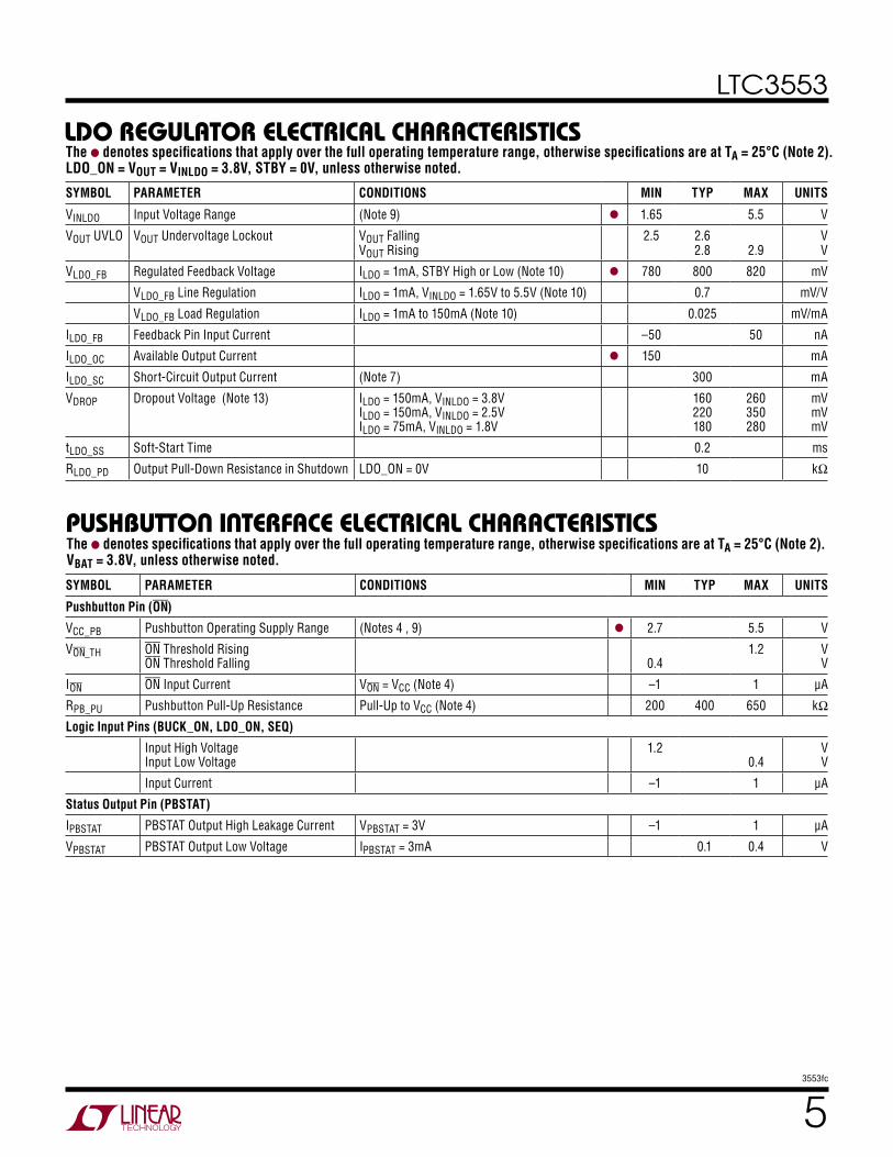
53553fc
SYMBOL PARAMETER CONDITIONS MIN TYP MAX UNITS
VINLDO Input Voltage Range (Note 9) l 1.65 5.5 V
VOUT UVLO VOUT Undervoltage Lockout VOUT Falling VOUT Rising
2.5 2.6 2.8
2.9
V V
VLDO_FB Regulated Feedback Voltage ILDO = 1mA, STBY High or Low (Note 10) l 780 800 820 mV
VLDO_FB Line Regulation ILDO = 1mA, VINLDO = 1.65V to 5.5V (Note 10) 0.7 mV/V
VLDO_FB Load Regulation ILDO = 1mA to 150mA (Note 10) 0.025 mV/mA
ILDO_FB Feedback Pin Input Current –50 50 nA
ILDO_OC Available Output Current l 150 mA
ILDO_SC Short-Circuit Output Current (Note 7) 300 mA
VDROP Dropout Voltage (Note 13) ILDO = 150mA, VINLDO = 3.8V ILDO = 150mA, VINLDO = 2.5V ILDO = 75mA, VINLDO = 1.8V
160 220 180
260 350 280
mV mV mV
tLDO_SS Soft-Start Time 0.2 ms
RLDO_PD Output Pull-Down Resistance in Shutdown LDO_ON = 0V 10 kΩ
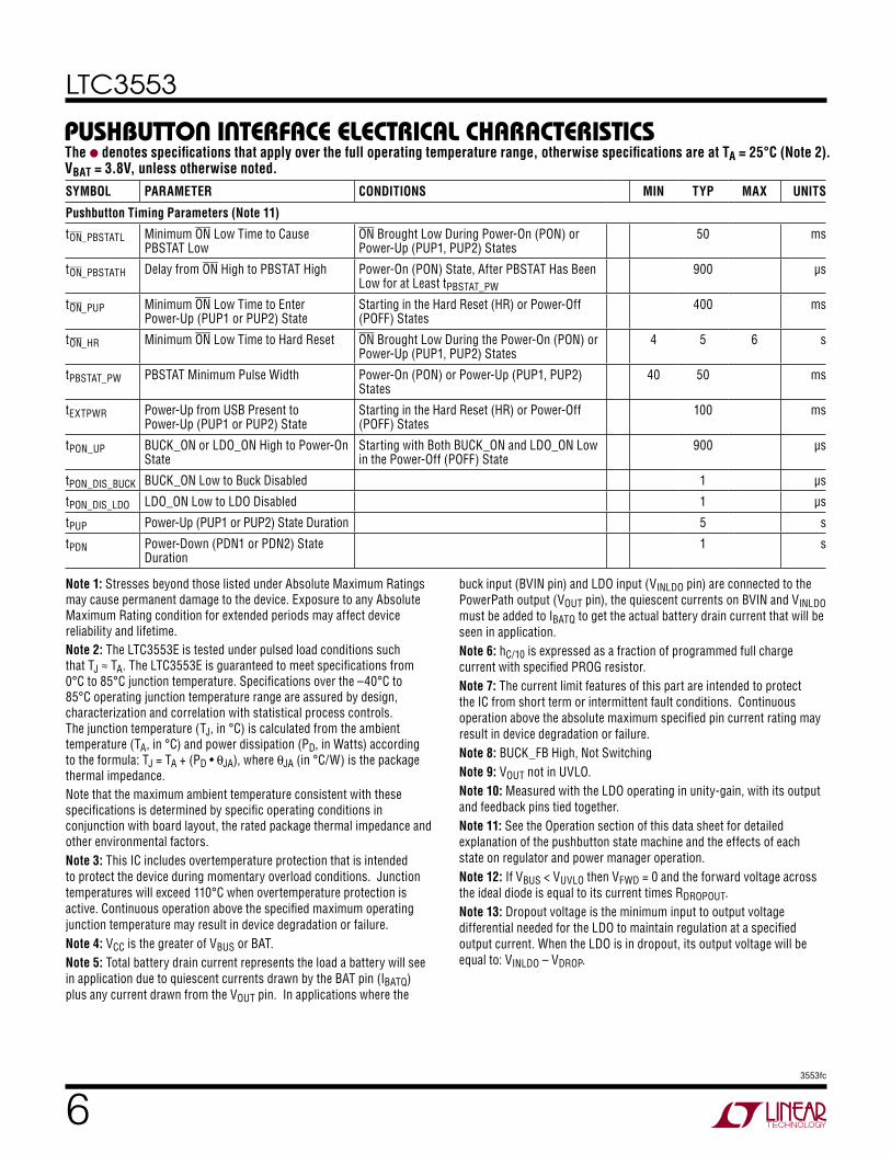
pushbuTTon inTerFace elecTrical characTerisTicsThe l denotes specifications that apply over the full operating temperature range, otherwise specifications are at TA = 25°C (Note 2). VBAT = 3.8V, unless otherwise noted.
lDo regulaTor elecTrical characTerisTicsThe l denotes specifications that apply over the full operating temperature range, otherwise specifications are at TA = 25°C (Note 2). LDO_ON = VOUT = VINLDO = 3.8V, STBY = 0V, unless otherwise noted.
SYMBOL PARAMETER CONDITIONS MIN TYP MAX UNITS
Pushbutton Pin (ON)
VCC_PB Pushbutton Operating Supply Range (Notes 4 , 9) l 2.7 5.5 V
VON_TH ON Threshold Rising ON Threshold Falling
0.4
1.2 V V
ION ON Input Current VON = VCC (Note 4) –1 1 µA
RPB_PU Pushbutton Pull-Up Resistance Pull-Up to VCC (Note 4) 200 400 650 kΩ
Logic Input Pins (BUCK_ON, LDO_ON, SEQ)
Input High Voltage Input Low Voltage
1.2 0.4
V V
Input Current –1 1 µA
Status Output Pin (PBSTAT)
IPBSTAT PBSTAT Output High Leakage Current VPBSTAT = 3V –1 1 µA
VPBSTAT PBSTAT Output Low Voltage IPBSTAT = 3mA 0.1 0.4 V
LTC3553
63553fc
Note 1: Stresses beyond those listed under Absolute Maximum Ratings may cause permanent damage to the device. Exposure to any Absolute Maximum Rating condition for extended periods may affect device reliability and lifetime.Note 2: The LTC3553E is tested under pulsed load conditions such that TJ ≈ TA. The LTC3553E is guaranteed to meet specifications from 0°C to 85°C junction temperature. Specifications over the –40°C to 85°C operating junction temperature range are assured by design, characterization and correlation with statistical process controls. The junction temperature (TJ, in °C) is calculated from the ambient temperature (TA, in °C) and power dissipation (PD, in Watts) according to the formula: TJ = TA + (PD • θJA), where θJA (in °C/W) is the package thermal impedance.Note that the maximum ambient temperature consistent with these specifications is determined by specific operating conditions in conjunction with board layout, the rated package thermal impedance and other environmental factors.Note 3: This IC includes overtemperature protection that is intended to protect the device during momentary overload conditions. Junction temperatures will exceed 110°C when overtemperature protection is active. Continuous operation above the specified maximum operating junction temperature may result in device degradation or failure.Note 4: VCC is the greater of VBUS or BAT.Note 5: Total battery drain current represents the load a battery will see in application due to quiescent currents drawn by the BAT pin (IBATQ) plus any current drawn from the VOUT pin. In applications where the
buck input (BVIN pin) and LDO input (VINLDO pin) are connected to the PowerPath output (VOUT pin), the quiescent currents on BVIN and VINLDO must be added to IBATQ to get the actual battery drain current that will be seen in application.Note 6: hC/10 is expressed as a fraction of programmed full charge current with specified PROG resistor.Note 7: The current limit features of this part are intended to protect the IC from short term or intermittent fault conditions. Continuous operation above the absolute maximum specified pin current rating may result in device degradation or failure.Note 8: BUCK_FB High, Not SwitchingNote 9: VOUT not in UVLO.Note 10: Measured with the LDO operating in unity-gain, with its output and feedback pins tied together.Note 11: See the Operation section of this data sheet for detailed explanation of the pushbutton state machine and the effects of each state on regulator and power manager operation.Note 12: If VBUS < VUVLO then VFWD = 0 and the forward voltage across the ideal diode is equal to its current times RDROPOUT.Note 13: Dropout voltage is the minimum input to output voltage differential needed for the LDO to maintain regulation at a specified output current. When the LDO is in dropout, its output voltage will be equal to: VINLDO – VDROP.
pushbuTTon inTerFace elecTrical characTerisTicsThe l denotes specifications that apply over the full operating temperature range, otherwise specifications are at TA = 25°C (Note 2). VBAT = 3.8V, unless otherwise noted.SYMBOL PARAMETER CONDITIONS MIN TYP MAX UNITS
Pushbutton Timing Parameters (Note 11)
tON_PBSTATL Minimum ON Low Time to Cause PBSTAT Low
ON Brought Low During Power-On (PON) or Power-Up (PUP1, PUP2) States
50 ms
tON_PBSTATH Delay from ON High to PBSTAT High Power-On (PON) State, After PBSTAT Has Been Low for at Least tPBSTAT_PW
900 µs
tON_PUP Minimum ON Low Time to Enter Power-Up (PUP1 or PUP2) State
Starting in the Hard Reset (HR) or Power-Off (POFF) States
400 ms
tON_HR Minimum ON Low Time to Hard Reset ON Brought Low During the Power-On (PON) or Power-Up (PUP1, PUP2) States
4 5 6 s
tPBSTAT_PW PBSTAT Minimum Pulse Width Power-On (PON) or Power-Up (PUP1, PUP2) States
40 50 ms
tEXTPWR Power-Up from USB Present to Power-Up (PUP1 or PUP2) State
Starting in the Hard Reset (HR) or Power-Off (POFF) States
100 ms
tPON_UP BUCK_ON or LDO_ON High to Power-On State
Starting with Both BUCK_ON and LDO_ON Low in the Power-Off (POFF) State
900 µs
tPON_DIS_BUCK BUCK_ON Low to Buck Disabled 1 µs
tPON_DIS_LDO LDO_ON Low to LDO Disabled 1 µs
tPUP Power-Up (PUP1 or PUP2) State Duration 5 s
tPDN Power-Down (PDN1 or PDN2) State Duration
1 s

LTC3553
73553fc
VBUS Supply Current vs Temperature
VBUS Supply Current vs Temperature (Suspend Mode)
Battery Drain Current vs Temperature
VBUS Current Limit vs Temperature
Typical perForMance characTerisTics TA = 25°C, unless otherwise specified.
TEMPERATURE (°C)–75
200
I BUS
(µA)
300
350
400
–25 25 50 150
3553 G01
250
–50 0 75 100 125
VBUS = 5VHPWR = L
TEMPERATURE (°C)–75
0
I BUS
(µA)
10
15
25
20
–25 25 50 150
3553 G02
5
–50 0 75 100 125
VBUS = 5V
TEMPERATURE (°C)–75
0
I BAT
(µA)
2
3
5
4
–25 25 50 150
3553 G04
1
–50 0 75 100 125
VBUS = 5VVBAT = 3.8V
TEMPERATURE (°C)–750
I VBU
S (m
A)
200
300
500
400
–25 25 50
3553 G05
100
–50 0 75 100 125
VBUS = 5V
HPWR = H
HPWR = L
Battery Drain Current vs Temperature (Suspend Mode)
VBUS and Battery Current vs Load Current
Battery Charge Current and Voltage vs Time
RON from VBUS to VOUT vs Temperature
Charge Current vs Temperature (Thermal Regulation)
TEMPERATURE (°C)–75 –50 –25 25 50 75 100 1501250
0.20
R ON
(Ω)
0.30
0.35
0.45
0.50
0.40
3553 G07
0.25
IOUT = 200mA
TEMPERATURE (°C)–50 –30 –10 30 50 70 90 13011010
0
BATT
ERY
DRAI
N CU
RREN
T (µ
A)
4
6
10
18
16
14
12
8
3553 G03
2
BUCK AND LDO ON
VBAT = 3.8VSTBY = 3.8VREGULATORS LOAD = 0mA
ONLY LDO ON
ONLY BUCK ON
BUCK AND LDO OFF
HARD RESET
LOAD CURRENT (mA)0 100 300 500400200
–100
CURR
ENT
(mA)
100
200
400
600
500
300
3553 G06
0
RPROG = 1.87k
IVBUS
ILOAD
IBAT(CHARGING)
IBAT(DISCHARGING)
TEMPERATURE (°C)–75
0
I BAT
(mA)
160
240
480
400
320
–25 25 50 150
3553 G08
80
–50 0 75 100 125
VBUS = 5VHPWR = HRPROG = 1.87k
TIME (hour)0
0
BATT
ERY
CURR
ENT
(mA)
VOLTAGE (V)
200
300
600
500
400
2 4 5
3553 G09
100
0
2
3
6
5
4
1
1 3 6 7 8
920mAhr CELLVBUS = 5VRPROG = 1.87k
CHRG
VBAT
SAFETY TIMERTERMINATION
C/10IBAT
LTC3553
83553fc
Typical perForMance characTerisTics
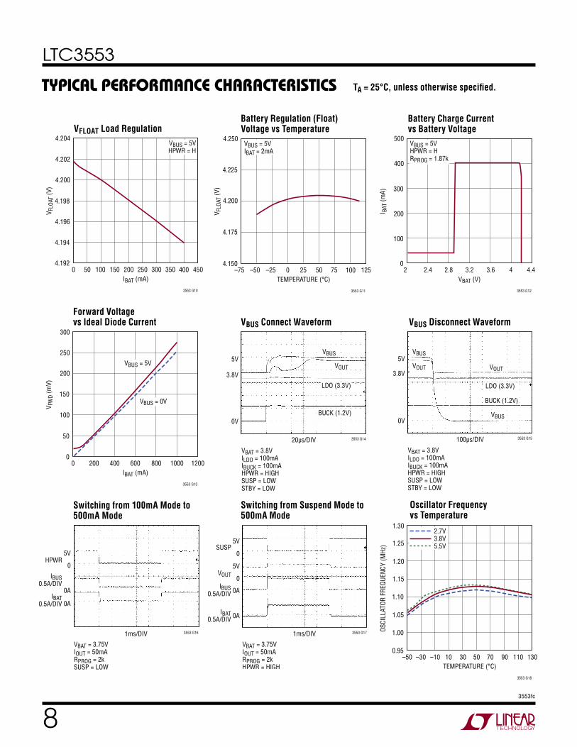
Battery Charge Current vs Battery Voltage
Forward Voltage vs Ideal Diode Current VBUS Connect Waveform VBUS Disconnect Waveform
VFLOAT Load RegulationBattery Regulation (Float) Voltage vs Temperature
TA = 25°C, unless otherwise specified.
IBAT (mA)0 50
4.192
V FLO
AT (V
)
4.196
4.198
4.204
4.202
4.200
200150 250 350 450400
3553 G10
4.194
100 300
VBUS = 5VHPWR = H
TEMPERATURE (°C)–75 –25–50
4.150
V FLO
AT (V
)
4.200
4.225
4.250
50 100 125
3553 G11
4.175
250 75
VBUS = 5VIBAT = 2mA
IBAT (mA)0 400200
0
V FW
D (m
V)
100
150
250
300
200
1000 1200
3553 G13
50
800600
VBUS = 5V
VBUS = 0V
VBAT = 3.8VILDO = 100mAIBUCK = 100mAHPWR = HIGHSUSP = LOWSTBY = LOW
20µs/DIV
5V
3.8V
BUCK (1.2V)
VBUS
VOUT
0V
3553 G14
LDO (3.3V)
VBAT = 3.8VILDO = 100mAIBUCK = 100mAHPWR = HIGHSUSP = LOWSTBY = LOW
3553 G15100µs/DIV
5V
3.8V
VBUS
VBUS
BUCK (1.2V)
VOUT VOUT
0V
LDO (3.3V)
Oscillator Frequency vs Temperature
Switching from Suspend Mode to 500mA Mode
VBAT = 3.75VIOUT = 50mARPROG = 2kHPWR = HIGH
3553 G171ms/DIV
5V
5V
SUSP
VOUT
0
0
0A
0A
IBUS0.5A/DIV
IBAT0.5A/DIV
Switching from 100mA Mode to 500mA Mode
VBAT = 3.75VIOUT = 50mARPROG = 2kSUSP = LOW
3553 G161ms/DIV
5VHPWR
0
0A
0A
IBUS0.5A/DIV
IBAT0.5A/DIV
VBAT (V)2 2.4 3.6 43.22.8
0
I BAT
(mA)
200
300
500
400
3553 G12
100
4.4
VBUS = 5VHPWR = HRPROG = 1.87k
TEMPERATURE (°C)–50 –30 –10 30 50 70 90 13011010
0.95
OSCI
LLAT
OR F
REQU
ENCY
(MHz
)
1.05
1.10
1.20
1.30
1.25
1.15
3553 G18
1.00
2.7V3.8V5.5V
LTC3553
93553fc
Typical perForMance characTerisTics
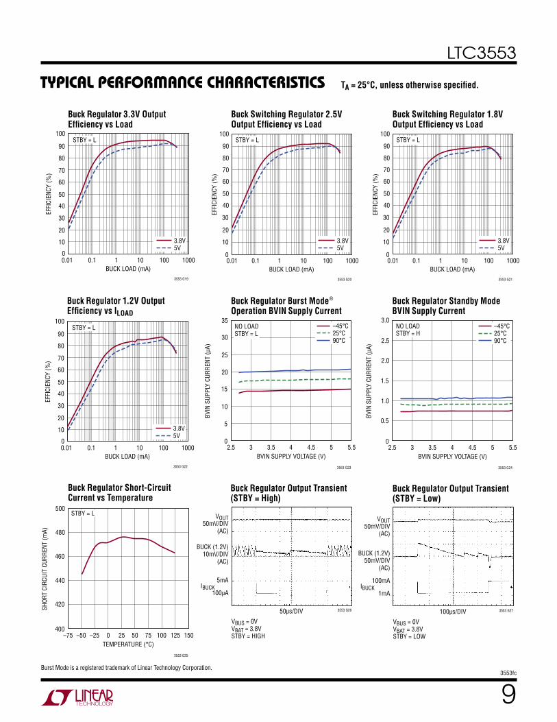
Buck Regulator Burst Mode® Operation BVIN Supply Current
Buck Regulator Standby Mode BVIN Supply Current
Buck Regulator 3.3V Output Efficiency vs Load
Buck Switching Regulator 1.8V Output Efficiency vs Load
TA = 25°C, unless otherwise specified.
Buck Switching Regulator 2.5V Output Efficiency vs Load
Buck Regulator 1.2V Output Efficiency vs ILOAD
BUCK LOAD (mA)0.01 0.10
EFFI
CIEN
CY (%
) 70
100
1 10 100 1000
3553 G19
60
50
40
30
20
10
80
90STBY = L
3.8V5V
BUCK LOAD (mA)0.01 0.10
EFFI
CIEN
CY (%
) 70
100
1 10 100 1000
3553 G22
60
50
40
30
20
10
80
90STBY = L
3.8V5V
BVIN SUPPLY VOLTAGE (V)2.5 3 4 4.5 5.553.5
0
BVIN
SUP
PLY
CURR
ENT
(µA)
10
15
25
35
30
20
3553 G23
5
NO LOADSTBY = L
–45°C25°C90°C
BVIN SUPPLY VOLTAGE (V)2.5 3 4 4.5 5.553.5
0
BVIN
SUP
PLY
CURR
ENT
(µA)
1.0
1.5
2.5
3.0
2.0
3553 G24
0.5
NO LOADSTBY = H
–45°C25°C90°C
BUCK LOAD (mA)
EFFI
CIEN
CY (%
)
3553 G20
0.01 0.1 100 10001010
20
30
80
40
50
60
90
100
70
10
STBY = L
3.8V5V
BUCK LOAD (mA)
EFFI
CIEN
CY (%
)
3553 G21
0.01 0.1 100 10001010
20
30
80
40
50
60
90
100
70
10
STBY = L
3.8V5V
Buck Regulator Short-Circuit Current vs Temperature
TEMPERATURE (°C)–75 –50 –25 25 50 75 100 1501250
400
SHOR
T CI
RCUI
T CU
RREN
T (m
A)
440
460
500
480
3553 G25
420
STBY = L
Buck Regulator Output Transient (STBY = High)
Buck Regulator Output Transient (STBY = Low)
VBUS = 0VVBAT = 3.8VSTBY = HIGH
VOUT50mV/DIV
(AC)
BUCK (1.2V)10mV/DIV
(AC)
5mA
100µAIBUCK
3553 G2650µs/DIV
Burst Mode is a registered trademark of Linear Technology Corporation.
VBUS = 0VVBAT = 3.8VSTBY = LOW
BUCK (1.2V)50mV/DIV
(AC)
VOUT50mV/DIV
(AC)
100mA
1mAIBUCK
3553 G27100µs/DIV

LTC3553
103553fc
Buck Regulator Switch Impedance vs Temperature
Typical perForMance characTerisTics
Buck Regulator Feedback Voltage vs Output Current
Power-Up Sequencing with SEQ Low
TA = 25°C, unless otherwise specified.
TEMPERATURE (°C)–75 –50 –25 25 50 75 100 1501250
0
SWIT
CH IM
PEDA
NCE
(Ω)
0.4
0.6
1.6
0.8
1.0
1.2
1.4
3553 G28
0.2
PMOS
NMOS
BVIN = 3.2VSTBY = L
OUTPUT CURRENT (mA)
FEED
BACK
VOL
TAGE
(V)
3553 G29
0.1 1 100 1000100.780
0.790
0.795
0.820
0.800
0.805
0.810
0.815
0.785
3.8V5VSTBY = L
Regulator Output Transient During STBY Transition
Buck Regulator Dropout Voltage in Standby Mode vs Load Current
LOAD CURRENT (mA)0 5 10 15 20 3025
0
DROP
OUT
VOLT
AGE
(mV)
40
60
100
120
140
160
180
200
80
3553 G32
20
–45°C25°C90°C
BVIN = 2.9V
BUCK OUTPUT0.5V/DIV
LDO OUTPUT1V/DIV
0V
0V
3553 G30100µs/DIV
FRONT PAGE APPLICATION CIRCUIT
BUCK OUTPUT0.5V/DIV
LDO OUTPUT1V/DIV
0V
0V
3553 G33100µs/DIV
FRONT PAGE APPLICATION CIRCUIT
Power-Up Sequencing with SEQ High
VBUS = 0VVBAT = 3.8V
BUCK OUTPUT1.2V AT 10mA
20mV/DIV (AC)
LDO OUTPUT3.3V AT 10mA
50mV/DIV (AC)
HIGH
LOWSTBY
3553 G3150µs/DIV
TEMPERATURE (°C)–50 –30 –10 30 50 70 90 13011010
780
FEED
BACK
VOL
TAGE
(mV)
790
795
820
800
805
810
815
3553 G34
785
VINLDO = 2.9VVINLDO = 3.8VVINLDO = 5V
100µA LDO LOAD
LDO LOAD (mA)25 50 75 100 1501250
796
LDO
OUTP
UT V
OLTA
GE (m
V)
798
799
800
801
3553 G35
797
LDO IN UNITY GAINVINLDO = 3.8VVOUT = VBAT = 3.8VVBUS = 0VSTBY = LOW
VINLDO (V)1 2 3 54
0
LDO
SHOR
T-CI
RCUI
T CU
RREN
T (m
A)
100
150
400
200
250
300
350
3553 G36
50
Regulated LDO Feedback Voltage vs Temperature LDO Load Regulation LDO Short-Circuit Current
LTC3553
113553fc
Typical perForMance characTerisTics TA = 25°C, unless otherwise specified.
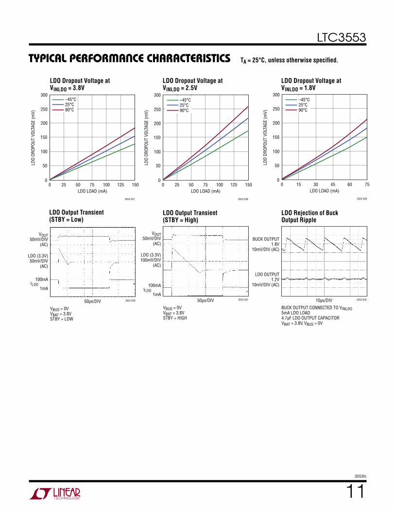
LDO Dropout Voltage at VINLDO = 3.8V
LDO LOAD (mA)25 50 75 100 1501250
0
LDO
DROP
OUT
VOLT
AGE
(mV)
100
150
200
250
300
3553 G37
50
–45°C25°C90°C
LDO Dropout Voltage at VINLDO = 2.5V
LDO LOAD (mA)25 50 75 100 1501250
0
LDO
DROP
OUT
VOLT
AGE
(mV)
100
150
200
250
300
3553 G38
50
–45°C25°C90°C
LDO LOAD (mA)15 30 45 60 750
0
LDO
DROP
OUT
VOLT
AGE
(mV)
100
150
200
250
300
3553 G39
50
–45°C25°C90°C
LDO Dropout Voltage at VINLDO = 1.8V
VBUS = 0VVBAT = 3.8VSTBY = LOW
VOUT50mV/DIV
(AC)
LDO (3.3V)50mV/DIV
(AC)
100mA
1mAILDO
3553 G4050µs/DIVVBUS = 0VVBAT = 3.8VSTBY = HIGH
VOUT50mV/DIV
(AC)
LDO (3.3V)100mV/DIV
(AC)
100mA
1mAILDO
3553 G4150µs/DIV
BUCK OUTPUT CONNECTED TO VINLDO5mA LDO LOAD4.7µF LDO OUTPUT CAPACITORVBAT = 3.8V, VBUS = 0V
BUCK OUTPUT1.8V
10mV/DIV (AC)
LDO OUTPUT1.2V
10mV/DIV (AC)
3553 G4210µs/DIV
LDO Output Transient (STBY = Low)
LDO Output Transient (STBY = High)
LDO Rejection of Buck Output Ripple

LTC3553
123553fc
HPWR (Pin 1): High Power Logic Input. When this pin is low the input current limit is set to 100mA and when this pin is driven high it is set to 500mA. The SUSP pin needs to be low for the input current limit circuit to be enabled. This pin has a conditional internal pull-down resistor when power is applied to the VBUS pin.
SEQ (Pin 2): Regulator Power-Up Sequence Select. While in the power off or hard reset states, a button press or application of USB bus power causes the pushbutton in-terface to temporarily enable both regulators. The state of the SEQ pin determines which regulator is enabled before the other. If SEQ is low, the buck regulator is enabled first. If SEQ is high, the LDO regulator is enabled first. The second regulator is enabled once the feedback voltage of the first regulator nears regulation. The SEQ pin must be tied to either VOUT or ground.
PBSTAT (Pin 3): Pushbutton Status. This open-drain output is a debounced and buffered version of the ON pushbut-ton input. It may be used to interrupt a microprocessor.
ON (Pin 4): Pushbutton Input. Weak internal pull-up forces a high state if ON is left floating. A normally open pushbutton is connected from ON to ground to force a low state on this pin.
LDO_ON (Pin 5): Logic Input Enables the Low Dropout (LDO) Regulator. This pin must be driven to a valid logic level. Do not float this pin.
STBY (Pin 6): Standby Mode. When this pin is driven high, the buck and LDO regulator quiescent current is reduced to very low levels, while still maintaining output voltage regulation. In this mode, the buck regulator is limited to 10mA maximum load current, and the LDO regulator’s response to line and load transients is slower. This pin must be driven to a valid logic level. Do not float this pin.
BUCK_ON (Pin 7): Logic Input Enables the Buck Regula-tor. This pin must be driven to a valid logic level. Do not float this pin.
BUCK_FB (Pin 8): Feedback Input for the Buck Regulator. This pin servos to a fixed voltage of 0.8V when the control loop is complete.
LDO_FB (Pin 9): Feedback Input for the Low Dropout Regulator. This pin servos to a fixed voltage of 0.8V when the control loop is complete.
LDO (Pin 10): Low Dropout (LDO) Linear Regulator Out-put. This pin should be bypassed with a low impedance multilayer ceramic capacitor.
VINLDO (Pin 11): Power Input Pin for the LDO Regulator. This pin is to be connected to VOUT or any supply volt-age below VOUT, such as the buck regulator output. This pin should be bypassed with a low impedance multilayer ceramic capacitor.
BVIN (Pin 12): Power Input for the Buck Regulator. It is recommended that this pin be connected to the VOUT pin. It should be bypassed with a low impedance multilayer ceramic capacitor.
SW (Pin 13): Power Transmission (Switch) Pin for the Buck Regulator.
CHRG (Pin 14): Open-Drain Charge Status Output. This pin indicates the status of the battery charger. It is internally pulled low while charging. Once the battery charge cur-rent reduces to less than one-tenth of the programmed charge current, this pin goes into a high impedance state. An external pull-up resistor and/or LED is required to provide indication.
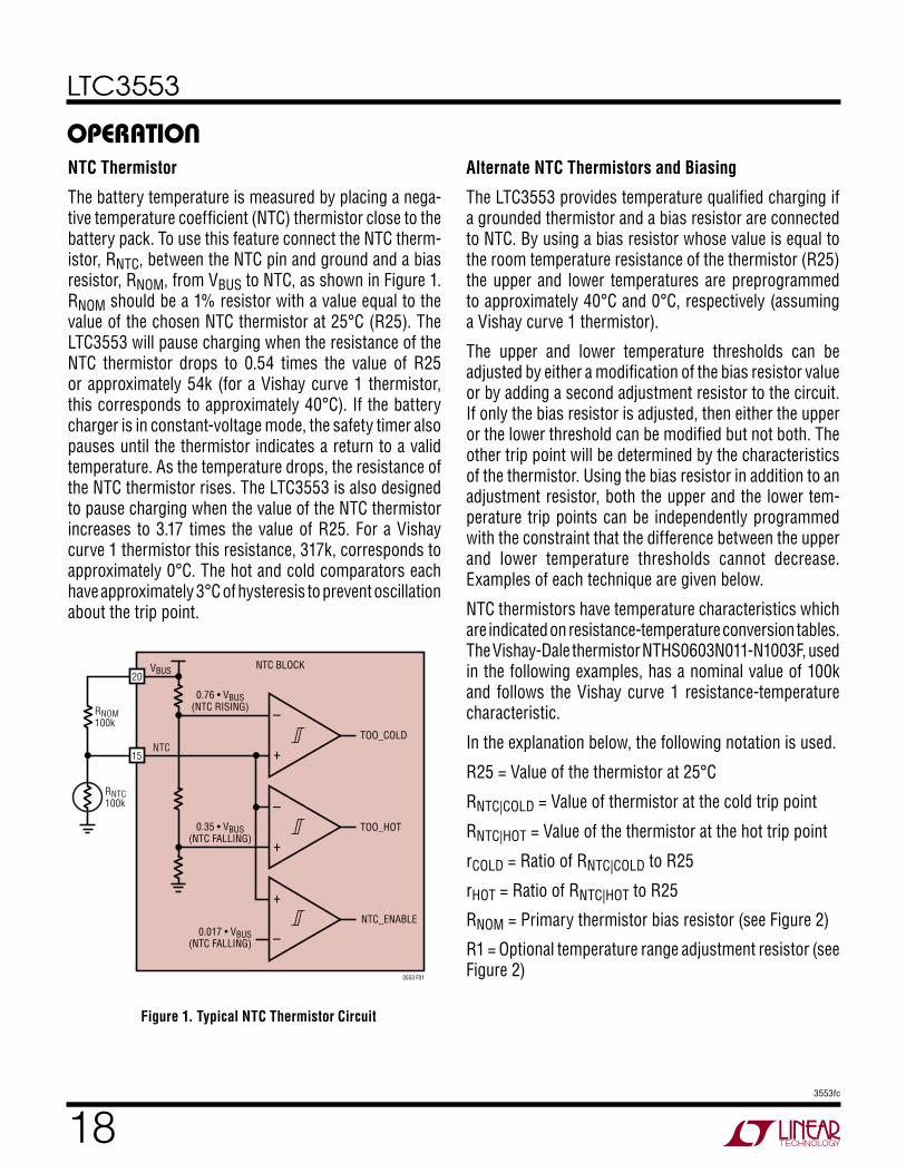
NTC (Pin 15): The NTC pin connects to a battery’s therm-istor to determine if the battery is too hot or too cold to charge. If the battery’s temperature is out of range, charging is paused until it drops back into range. A low drift bias resistor is required from VBUS to NTC and a thermistor is required from NTC to ground. If the NTC function is not desired, the NTC pin should be grounded.
PROG (Pin 16): Charge Current Program and Charge Current Monitor Pin. Connecting a resistor from PROG to ground programs the charge current as given by:
ICHG (A)= 750V
RPROG
If sufficient input power is available in constant-current mode, this pin servos to 1V. The voltage on this pin always represents the actual charge current.
pin FuncTions

LTC3553
133553fc
pin FuncTionsBAT (Pin 17): Single-Cell Li-Ion Battery Pin. Depending on available power and load, a Li-Ion battery on BAT will either deliver system power to VOUT through the ideal diode or be charged from the battery charger.
VOUT (Pin 18): Output Voltage of the PowerPath Controller and Input Voltage of the Battery Charger. The majority of the portable products should be powered from VOUT. The LTC3553 will partition the available power between the external load on VOUT and the internal battery charger. Priority is given to the external load and any extra power is used to charge the battery. An ideal diode from BAT to VOUT ensures that VOUT is powered even if the load exceeds the allotted input current from VBUS or if the VBUS power source is removed. VOUT should be bypassed with a low impedance multilayer ceramic capacitor.
SUSP (Pin 19): Suspend Mode Logic Input. If this pin is driven high the input current limit path is disabled. In this state the circuit draws negligible power from the VBUS pin. Any load at the VOUT pin is provided by the battery through the internal ideal diode. When this input is grounded, the input current limit will be set to desired value as determined by the state of the HPWR pin. This pin has a conditional internal pull-down resistor when power is applied to the VBUS pin.
VBUS (Pin 20): USB Input Voltage. VBUS will usually be connected to the USB port of a computer or a DC output wall adapter. VBUS should be bypassed with a low imped-ance multilayer ceramic capacitor.
GND (Exposed Pad Pin 21): Ground. The exposed pack-age pad is ground and must be soldered to the PC board for proper functionality and for maximum heat transfer.
LTC3553
143553fc
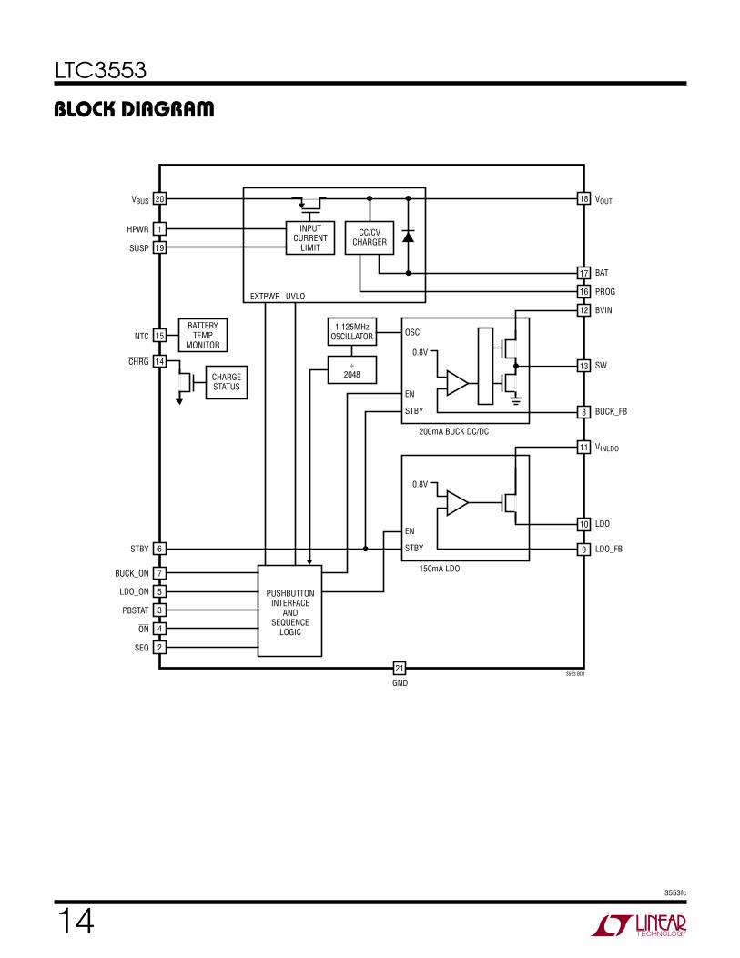
blocK DiagraM
0.8V
150mA LDO
EN
STBY
INPUTCURRENT
LIMIT
CC/CVCHARGER
BATTERYTEMP
MONITOR
PUSHBUTTONINTERFACE
ANDSEQUENCE
LOGIC
1.125MHzOSCILLATOR
CHARGESTATUS
0.8V
OSC
VBUS VOUT
BAT
PROG
SW
BUCK_FB
VINLDO
LDO
LDO_FB
HPWR
SUSP
NTC
EXTPWR UVLO
STBY
GND3553 BD1
BUCK_ON
LDO_ON
PBSTAT
ON
CHRG
200mA BUCK DC/DC
EN
STBY
SEQ
20 18
17
16
BVIN12
13
8
11
10
9
1
19
15
14
6
21
7
5
3
4
2
÷2048
LTC3553
153553fc
Introduction
The LTC3553 is a highly integrated power management IC that includes the following features:
PowerPath controller
Battery charger
Ideal diode
Pushbutton controller
200mA buck regulator
150mA low dropout (LDO) linear regulator
Designed specifically for USB applications, the PowerPath controller incorporates a precision input current limit which communicates with the battery charger to ensure that input current never violates the USB specifications. The ideal diode from BAT to VOUT guarantees that ample power is always available to VOUT even if there is insufficient or absent power at VBUS. The LTC3553 also includes a pushbutton input to control the two regulators and system reset. The constant-frequency current mode step-down switching regulator provides 200mA and supports 100% duty cycle operation as well as Burst Mode operation for high efficiency at light load. No external compensation components are required for the switching regulator. The LDO can deliver up to 150mA, and is stable with a ceramic output capacitor of at least 1µF. For application flexibility, the LDO’s power input pin, VINLDO, is independent of the buck’s BVIN pin. The LDO can be powered by the buck output or be driven by the PowerPath VOUT.
Either regulator can be programmed for a minimum output voltage of 0.8V and can be used to power a microcontroller core, microcontroller I/O, memory or other logic circuitry.
The buck regulator operates at 1.125MHz. Both regulators include a low power standby mode which can be used to power essential keep-alive circuitry while draining ultralow current from the battery for extended battery life.
USB PowerPath Controller
The input current limit and charger control circuits of the LTC3553 are designed to limit input current as well as control battery charge current as a function of IVOUT. VOUT drives the combination of the external load, the buck and LDO regulators and the battery charger.
If the combined load does not exceed the programmed input current limit, VOUT will be connected to VBUS through an internal 350mΩ P-channel MOSFET. If the combined load at VOUT exceeds the programmed input current limit, the battery charger will reduce its charge current by the amount necessary to enable the external load to be satisfied while maintaining the programmed input current. Even if the battery charge current is set to exceed the allowable USB current, the average input current USB specification will not be violated. Furthermore, load current at VOUT will always be prioritized and only excess available current will be used to charge the battery.
The input current limit is programmed by the HPWR and SUSP pins. If SUSP pin set high, the input current limit is disabled. If SUSP pin is low, the input current limit is enabled. HPWR pin selects between 100mA input current limit when it is low and 500mA input current limit when it is high.
Ideal Diode From BAT to VOUT
The LTC3553 has an internal ideal diode from BAT to VOUT designed to respond quickly whenever VOUT drops below BAT. If the load increases beyond the input current limit, additional current will be pulled from the battery via the ideal diode. Furthermore, if power to VBUS (USB) is removed, then all of the application power will be provided by the battery via the ideal diode. The ideal diode is fast enough to keep VOUT from dropping significantly with just the recommended output capacitor. The ideal diode consists of a precision amplifier that enables an on-chip P-channel
operaTion
Simplified PowerPath Block Diagram
100mA/500mAINPUT CURRENT
LIMIT
CC/CVCHARGER 15mV
IDEAL
3553 F01a
+–
VOUT18VBUS 20
BAT17

LTC3553
163553fc
MOSFET whenever the voltage at VOUT is approximately 15mV (VFWD) below the voltage at BAT. The resistance of the internal ideal diode is approximately 240mΩ.
Suspend Mode
When the SUSP pin is pulled high the LTC3553 enters suspend mode to comply with the USB specification. In this mode, the power path between VBUS and VOUT is put in a high impedance state to reduce the VBUS input current to 15μA. The system load connected to VOUT is supplied through the ideal diode connected to BAT.
VBUS Undervoltage Lockout (UVLO) and Undervoltage Current Limit (UVCL)
An internal undervoltage lockout circuit monitors VBUS and keeps the input current limit circuitry off until VBUS rises above the rising UVLO threshold (3.8V) and at least 200mV above VBAT. Hysteresis on the UVLO turns off the input current limit circuitry if VBUS drops below 3.6V or within 50mV of VBAT. When this happens, system power at VOUT will be drawn from the battery via the ideal diode. To minimize the possibility of oscillation in and out of UVLO when using resistive input supplies, the input current limit is reduced as VBUS falls below 4.45V typical.
Battery Charger
The LTC3553 includes a constant-current/constant-volt-age battery charger with automatic recharge, automatic termination by safety timer, low voltage trickle charging, bad cell detection and thermistor sensor input for out of temperature charge pausing. When a battery charge cycle begins, the battery charger first determines if the battery is deeply discharged. If the battery voltage is below VTRKL, typically 2.9V, an automatic trickle charge feature sets the battery charge current to 10% of the programmed value. If the low voltage persists for more than 1/2 hour, the battery charger automatically terminates. Once the battery voltage is above 2.9V, the battery charger begins charging in full power constant current mode. The current delivered to the battery will try to reach 750V/RPROG. Depending on available input power and external load conditions, the battery charger may or may not be able to charge at the full programmed current. The external load will always be
prioritized over the battery charge current. The USB cur-rent limit programming will always be observed and only additional current will be available to charge the battery. When system loads are light, battery charge current will be maximized.
Charge Termination
The battery charger has a built-in safety timer. When the battery voltage approaches the float voltage, the charge current begins to decrease as the LTC3553 enters constant-voltage mode. Once the battery charger detects that it has entered constant-voltage mode, the four hour safety timer is started. After the safety timer expires, charging of the battery will terminate and no more current will be delivered to the battery.
Automatic Recharge
After the battery charger terminates, it will remain off drawing only microamperes of current from the battery. If the portable product remains in this state long enough, the battery will eventually self discharge. To ensure that the battery is always topped off, a charge cycle will au-tomatically begin when the battery voltage falls below VRECHRG (typically 4.1V). In the event that the safety timer is running when the battery voltage falls below VRECHRG, the timer will reset back to zero. To prevent brief excur-sions below VRECHRG from resetting the safety timer, the battery voltage must be below VRECHRG for approximately 2ms. The charge cycle and safety timer will also restart if the VBUS UVLO cycles low and then high (e.g., VBUS, is removed and then replaced).
Charge Current
The charge current is programmed using a single resis-tor from PROG to ground. 1/750th of the battery charge current is delivered to PROG which will attempt to servo to 1.000V. Thus, the battery charge current will try to reach 750 times the current in the PROG pin. The program resistor and the charge current are calculated using the following equations:
RPROG = 750V
ICHG,ICHG = 750V
RPROG
operaTion
LTC3553
173553fc
In either the constant-current or constant-voltage charg-ing modes, the PROG pin voltage will be proportional to the actual charge current delivered to the battery. There-fore, the actual charge current can be determined at any time by monitoring the PROG pin voltage and using the following equation:
I BAT = VPROG
RPROG• 750
In many cases, the actual battery charge current, IBAT, will be lower than ICHG due to limited input current available and prioritization with the system load drawn from VOUT.
Thermal Regulation
To prevent thermal damage to the IC or surrounding components, an internal thermal feedback loop will automatically decrease the programmed charge cur-rent if the die temperature rises to approximately 110°C. Thermal regulation protects the LTC3553 from excessive temperature due to high power operation or high ambient thermal conditions and allows the user to push the limits of the power handling capability with a given circuit board design without risk of damaging the LTC3553 or external components. The benefit of the LTC3553 thermal regula-tion loop is that charge current can be set according to the desired charge rate rather than worst-case conditions with the assurance that the battery charger will automatically reduce the current in worst-case conditions.
Charge Status Indication
The CHRG pin indicates the status of the battery charger. An open-drain output, the CHRG pin can drive an indicator LED through a current limiting resistor for human interfacing or simply a pull-up resistor for microprocessor interfacing. When charging begins, CHRG is pulled low and remains low for the duration of a normal charge cycle. When charg-ing is complete, i.e., the charger enters constant-voltage mode and the charge current has dropped to one-tenth of the programmed value, the CHRG pin is released (high impedance). The CHRG pin does not respond to the C/10 threshold if the LTC3553 reduces the charge current due
to excess load on the VOUT pin. This prevents false end of charge indications due to insufficient power available to the battery charger. Even though charging is stopped during an NTC fault the CHRG pin will stay low indicating that charging is not complete.
Battery Charger Stability Considerations
The LTC3553’s battery charger contains both a constant-voltage and a constant-current control loop. The constant-voltage loop is stable without any compensation when a battery is connected with low impedance leads. Excessive lead length, however, may add enough series inductance to require a bypass capacitor of at least 1μF from BAT to GND. Furthermore, a 100μF 1210 ceramic capacitor in series with a 0.3Ω resistor from BAT to GND is required to keep ripple voltage low if operation with the battery disconnected is allowed.
High value, low ESR multilayer ceramic chip capacitors reduce the constant-voltage loop phase margin, possibly resulting in instability. Ceramic capacitors up to 22μF may be used in parallel with a battery, but larger ceramics should be decoupled with 0.2Ω to 1Ω of series resistance.
In constant-current mode, the PROG pin is in the feed-back loop rather than the battery voltage. Because of the additional pole created by any PROG pin capacitance, capacitance on this pin must be kept to a minimum. With no additional capacitance on the PROG pin, the battery charger is stable with program resistor values as high as 25k. However, additional capacitance on this node reduces the maximum allowed program resistor. The pole frequency at the PROG pin should be kept above 100kHz. Therefore, if the PROG pin has a parasitic capacitance, CPROG, the following equation should be used to calculate the maximum resistance value for RPROG:
RPROG ≤ 1
2π •100kHz •CPROG
operaTion
LTC3553
183553fc
NTC Thermistor
The battery temperature is measured by placing a nega-tive temperature coefficient (NTC) thermistor close to the battery pack. To use this feature connect the NTC therm-istor, RNTC, between the NTC pin and ground and a bias resistor, RNOM, from VBUS to NTC, as shown in Figure 1. RNOM should be a 1% resistor with a value equal to the value of the chosen NTC thermistor at 25°C (R25). The LTC3553 will pause charging when the resistance of the NTC thermistor drops to 0.54 times the value of R25 or approximately 54k (for a Vishay curve 1 thermistor, this corresponds to approximately 40°C). If the battery charger is in constant-voltage mode, the safety timer also pauses until the thermistor indicates a return to a valid temperature. As the temperature drops, the resistance of the NTC thermistor rises. The LTC3553 is also designed to pause charging when the value of the NTC thermistor increases to 3.17 times the value of R25. For a Vishay curve 1 thermistor this resistance, 317k, corresponds to approximately 0°C. The hot and cold comparators each have approximately 3°C of hysteresis to prevent oscillation about the trip point.
Alternate NTC Thermistors and Biasing
The LTC3553 provides temperature qualified charging if a grounded thermistor and a bias resistor are connected to NTC. By using a bias resistor whose value is equal to the room temperature resistance of the thermistor (R25) the upper and lower temperatures are preprogrammed to approximately 40°C and 0°C, respectively (assuming a Vishay curve 1 thermistor).
The upper and lower temperature thresholds can be adjusted by either a modification of the bias resistor value or by adding a second adjustment resistor to the circuit. If only the bias resistor is adjusted, then either the upper or the lower threshold can be modified but not both. The other trip point will be determined by the characteristics of the thermistor. Using the bias resistor in addition to an adjustment resistor, both the upper and the lower tem-perature trip points can be independently programmed with the constraint that the difference between the upper and lower temperature thresholds cannot decrease. Examples of each technique are given below.
NTC thermistors have temperature characteristics which are indicated on resistance-temperature conversion tables. The Vishay-Dale thermistor NTHS0603N011-N1003F, used in the following examples, has a nominal value of 100k and follows the Vishay curve 1 resistance-temperature characteristic.
In the explanation below, the following notation is used.
R25 = Value of the thermistor at 25°C
RNTC|COLD = Value of thermistor at the cold trip point
RNTC|HOT = Value of the thermistor at the hot trip point
rCOLD = Ratio of RNTC|COLD to R25
rHOT = Ratio of RNTC|HOT to R25
RNOM = Primary thermistor bias resistor (see Figure 2)
R1 = Optional temperature range adjustment resistor (see Figure 2)
operaTion
Figure 1. Typical NTC Thermistor Circuit
–
+
–
+
RNOM100k
RNTC100k
NTC
VBUS
NTC_ENABLE
3553 F01
NTC BLOCK
TOO_COLD
TOO_HOT
0.76 • VBUS(NTC RISING)
0.35 • VBUS(NTC FALLING)
0.017 • VBUS(NTC FALLING)
–
+
20
15

LTC3553
193553fc
By using a bias resistor, RNOM, different in value from R25, the hot and cold trip points can be moved in either direction. The temperature span will change somewhat due to the nonlinear behavior of the thermistor. The following equations can be used to easily calculate a new value for the bias resistor:
RNOM = r HOT0.538
•R25
RNOM = r COLD3.17
•R25
where rHOT and rCOLD are the resistance ratios at the de-sired hot and cold trip points. Note that these equations are linked. Therefore, only one of the two trip points can be independently set, the other is determined by the de-fault ratios designed in the IC.
Consider an example where a 60°C hot trip point is desired. From the Vishay curve 1 R-T characteristics, rHOT is 0.2488 at 60°C. Using the above equation, RNOM should be set to 46.4k. With this value of RNOM, the cold trip point is about 16°C. Notice that the span is now 44°C rather than the previous 40°C. This is due to the decrease in temperature gain of the thermistor as absolute temperature increases.
The upper and lower temperature trip points can be in-dependently programmed by using an additional bias resistor as shown in Figure 2. The following formulas can be used to compute the values of RNOM and R1:
RNOM =r COLD – r HOT
2.714• R25
R1 = 0.536 • RNOM – r HOT • R25
For example, to set the trip points to 0°C and 45°C with a Vishay curve 1 thermistor choose:
RNOM = 3.266 – 0.4368
2.714• 100k = 104.2k
the nearest 1% value is 105k:
R1 = 0.536 • 105k – 0.4368 • 100k = 12.6k
The nearest 1% value is 12.7k. The final solution is shown in Figure 2 and results in an upper trip point of 45°C and a lower trip point of 0°C.
operaTion
Figure 2. NTC Thermistor Circuit With Additional Bias Resistor
–
+
–
+
RNOM105k
RNTC100k
R112.7k
NTC
VBUS
NTC_ENABLE
3553 F02
TOO_COLD
TOO_HOT
0.76 • VBUS(NTC RISING)
0.35 • VBUS(NTC FALLING)
0.017 • VBUS(NTC FALLING)
–
+
20
15
The trip points for the LTC3553’s temperature qualifica-tion are internally programmed at 0.35 • VBUS for the hot threshold and 0.76 • VBUS for the cold threshold.
Therefore, the hot trip point is set when:
RNTC|HOT
RNOM +RNTC|HOT• VBUS = 0.35 • VBUS
and the cold trip point is set when:
RNTC|COLD
RNOM +RNTC|COLD• VBUS = 0.76 • VBUS
Solving these equations for RNTC|COLD and RNTC|HOT results in the following:
RNTC|HOT = 0.538 • RNOM
and
RNTC|COLD = 3.17 • RNOM
By setting RNOM equal to R25, the above equations result in rHOT = 0.538 and rCOLD = 3.17. Referencing these ratios to the Vishay Resistance-Temperature Curve 1 chart gives a hot trip point of about 40°C and a cold trip point of about 0°C. The difference between the hot and cold trip points is approximately 40°C.
LTC3553
203553fc
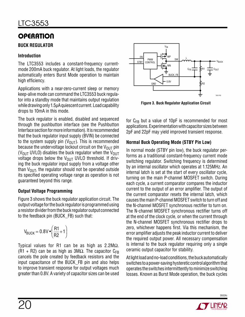
operaTionBUCK REGULATOR
Introduction
The LTC3553 includes a constant-frequency current-mode 200mA buck regulator. At light loads, the regulator automatically enters Burst Mode operation to maintain high efficiency.
Applications with a near-zero-current sleep or memory keep-alive mode can command the LTC3553 buck regula-tor into a standby mode that maintains output regulation while drawing only 1.5µA quiescent current. Load capability drops to 10mA in this mode.
The buck regulator is enabled, disabled and sequenced through the pushbutton interface (see the Pushbutton Interface section for more information). It is recommended that the buck regulator input supply (BVIN) be connected to the system supply pin (VOUT). This is recommended because the undervoltage lockout circuit on the VOUT pin (VOUT UVLO) disables the buck regulator when the VOUT voltage drops below the VOUT UVLO threshold. If driv-ing the buck regulator input supply from a voltage other than VOUT, the regulator should not be operated outside its specified operating voltage range as operation is not guaranteed beyond this range.
Output Voltage Programming
Figure 3 shows the buck regulator application circuit. The output voltage for the buck regulator is programmed using a resistor divider from the buck regulator output connected to the feedback pin (BUCK_FB) such that:
VBUCK = 0.8V • R1
R2+ 1
Typical values for R1 can be as high as 2.2MΩ. (R1 + R2) can be as high as 3MΩ. The capacitor CFB cancels the pole created by feedback resistors and the input capacitance of the BUCK_FB pin and also helps to improve transient response for output voltages much greater than 0.8V. A variety of capacitor sizes can be used
for CFB but a value of 10pF is recommended for most applications. Experimentation with capacitor sizes between 2pF and 22pF may yield improved transient response.
Normal Buck Operating Mode (STBY Pin Low)
In normal mode (STBY pin low), the buck regulator per-forms as a traditional constant-frequency current mode switching regulator. Switching frequency is determined by an internal oscillator which operates at 1.125MHz. An internal latch is set at the start of every oscillator cycle, turning on the main P-channel MOSFET switch. During each cycle, a current comparator compares the inductor current to the output of an error amplifier. The output of the current comparator resets the internal latch, which causes the main P-channel MOSFET switch to turn off and the N-channel MOSFET synchronous rectifier to turn on. The N-channel MOSFET synchronous rectifier turns off at the end of the clock cycle, or when the current through the N-channel MOSFET synchronous rectifier drops to zero, whichever happens first. Via this mechanism, the error amplifier adjusts the peak inductor current to deliver the required output power. All necessary compensation is internal to the buck regulator requiring only a single ceramic output capacitor for stability.
At light load and no-load conditions, the buck automatically switches to a power-saving hysteretic control algorithm that operates the switches intermittently to minimize switching losses. Known as Burst Mode operation, the buck cycles
Figure 3. Buck Regulator Application Circuit
3553 F03
0.8V
VIN
CFB COUT
VBUCK
MP
MN
GND
BUCK_FB
R1
SW LPWMCONTROL
EN
STBY
R2
LTC3553
213553fc
the power switches enough times to charge the output capacitor to a voltage slightly higher than the regulation point. The buck then goes into a reduced quiescent current sleep mode. In this state, power loss is minimized while the load current is supplied by the output capacitor. Whenever the output voltage drops below a predetermined value, the buck wakes from sleep and cycles the switches again until the output capacitor voltage is once again slightly above the regulation point. Sleep time thus depends on load current, since the load current determines the discharge rate of the output capacitor.
Standby Mode Buck Operation (STBY Pin High)
There are situations where even the low quiescent current of Burst Mode operation is not low enough. For instance, in a static memory keep alive situation, load current may fall well below 1µA. In this case, the 22µA typical BVIN quiescent current in Burst Mode operation becomes the main factor determining battery run time.
Standby mode cuts BVIN quiescent current down to just 1.5µA, greatly extending battery run time in this essen-tially no-load region of operation. The application circuit commands the LTC3553 into and out of standby mode via the STBY pin logic input. Bringing the STBY pin high places the regulator into standby mode, while bringing it low returns it to Burst Mode operation. In standby mode, buck load capability drops to 10mA.
In standby mode, the buck regulator operates hyster-etically. When the BUCK_FB pin voltage falls below the internal 0.8V reference, a current source from BVIN to SW turns on, delivering current through the inductor to the switching regulator output capacitor and load. When the FB pin voltage rises above the reference plus a small hysteresis voltage, that current is shut off. In this way, output regulation is maintained.
Since the power transfer from BVIN to SW is through a high impedance current source rather than through a low impedance MOSFET switch, power loss scales with load current as in a linear low dropout (LDO) regulator, rather than as in a switching regulator. For near-zero load condi-tions where regulator quiescent current is the dominant power loss, standby mode is ideal. But at any appreciable
load current, Burst Mode operation yields the best overall conversion efficiency.
Shutdown
The buck regulator is shut down and enabled via the pushbutton interface. In shutdown, it draws only a few nanoamps of leakage current from the BVIN pin. It also pulls down on its output with a 10k resistor from its switch pin to ground.
Dropout Operation
It is possible for the buck regulator’s input voltage to fall near or below its programmed output voltage (e.g., a bat-tery voltage of 3.4V with a programmed output voltage of 3.3V). When this happens, the PMOS switch duty cycle increases to 100%, keeping the switch on continuously. Known as dropout operation, the output voltage equals the regulator’s input voltage minus the voltage drops across the internal P-channel MOSFET and the inductor.
Soft-Start Operation
In normal operating mode, soft-start works by gradually increasing the maximum allowed peak inductor current for the buck regulator over a 500μs period. This allows the output to rise slowly, helping minimize the inrush current needed to charge up the output capacitor. A soft-start cycle occurs whenever the buck is enabled.
Soft-start occurs only in normal operation, but not in standby mode. Standby mode operation is already in-herently current-limited, since the regulator works by intermittently turning on a current source from BVIN to SW. Changing the state of the STBY pin while the regula-tors are operating doesn’t trigger a new soft-start cycle, to avoid glitching the outputs.
Inductor Selection
Many different sizes and shapes of inductors are avail-able from numerous manufacturers. Choosing the right inductor from such a large selection of devices can be overwhelming, but following a few basic guidelines will make the selection process much simpler.
operaTion
LTC3553
223553fc
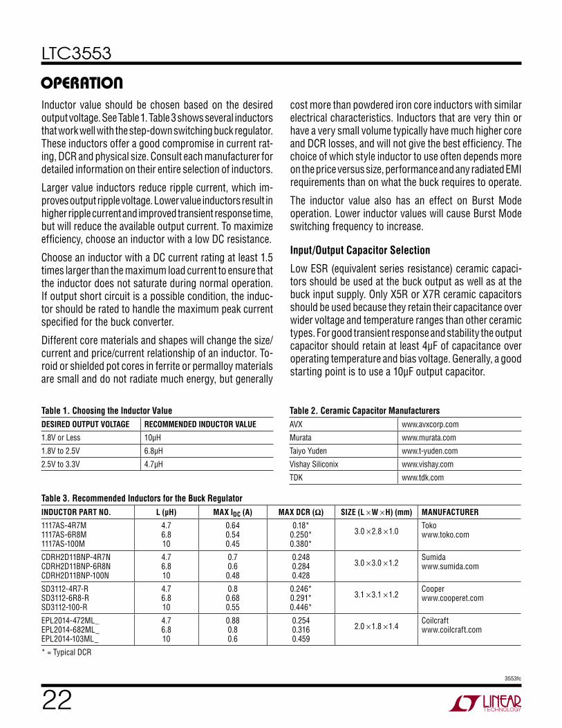
Inductor value should be chosen based on the desired output voltage. See Table 1. Table 3 shows several inductors that work well with the step-down switching buck regulator. These inductors offer a good compromise in current rat-ing, DCR and physical size. Consult each manufacturer for detailed information on their entire selection of inductors.
Larger value inductors reduce ripple current, which im-proves output ripple voltage. Lower value inductors result in higher ripple current and improved transient response time, but will reduce the available output current. To maximize efficiency, choose an inductor with a low DC resistance.
Choose an inductor with a DC current rating at least 1.5 times larger than the maximum load current to ensure that the inductor does not saturate during normal operation. If output short circuit is a possible condition, the induc-tor should be rated to handle the maximum peak current specified for the buck converter.
Different core materials and shapes will change the size/current and price/current relationship of an inductor. To-roid or shielded pot cores in ferrite or permalloy materials are small and do not radiate much energy, but generally
cost more than powdered iron core inductors with similar electrical characteristics. Inductors that are very thin or have a very small volume typically have much higher core and DCR losses, and will not give the best efficiency. The choice of which style inductor to use often depends more on the price versus size, performance and any radiated EMI requirements than on what the buck requires to operate.
The inductor value also has an effect on Burst Mode operation. Lower inductor values will cause Burst Mode switching frequency to increase.
Input/Output Capacitor Selection
Low ESR (equivalent series resistance) ceramic capaci-tors should be used at the buck output as well as at the buck input supply. Only X5R or X7R ceramic capacitors should be used because they retain their capacitance over wider voltage and temperature ranges than other ceramic types. For good transient response and stability the output capacitor should retain at least 4μF of capacitance over operating temperature and bias voltage. Generally, a good starting point is to use a 10μF output capacitor.
operaTion
Table 3. Recommended Inductors for the Buck RegulatorINDUCTOR PART NO. L (µH) MAX IDC (A) MAX DCR (Ω) SIZE (L × W × H) (mm) MANUFACTURER
1117AS-4R7M 1117AS-6R8M 1117AS-100M
4.7 6.8 10
0.64 0.54 0.45
0.18* 0.250* 0.380*
3.0 × 2.8 × 1.0Toko www.toko.com
CDRH2D11BNP-4R7N CDRH2D11BNP-6R8N CDRH2D11BNP-100N
4.7 6.8 10
0.7 0.6 0.48
0.248 0.284 0.428
3.0 × 3.0 × 1.2Sumida www.sumida.com
SD3112-4R7-R SD3112-6R8-R SD3112-100-R
4.7 6.8 10
0.8 0.68 0.55
0.246* 0.291* 0.446*
3.1 × 3.1 × 1.2Cooper www.cooperet.com
EPL2014-472ML_ EPL2014-682ML_ EPL2014-103ML_
4.7 6.8 10
0.88 0.8 0.6
0.254 0.316 0.459
2.0 × 1.8 × 1.4Coilcraft www.coilcraft.com
* = Typical DCR
Table 2. Ceramic Capacitor ManufacturersAVX www.avxcorp.com
Murata www.murata.com
Taiyo Yuden www.t-yuden.com
Vishay Siliconix www.vishay.com
TDK www.tdk.com
Table 1. Choosing the Inductor ValueDESIRED OUTPUT VOLTAGE RECOMMENDED INDUCTOR VALUE
1.8V or Less 10µH
1.8V to 2.5V 6.8µH
2.5V to 3.3V 4.7µH
LTC3553
233553fc
The switching regulator input supply should be bypassed with a 2.2μF capacitor. Consult with capacitor manu-facturers for detailed information on their selection and specifications of ceramic capacitors. Many manufacturers now offer very thin (<1mm tall) ceramic capacitors ideal for use in height-restricted designs. Table 2 shows a list of several ceramic capacitor manufacturers.
LOW DROPOUT LINEAR REGULATOR (LDO)
The LDO regulator supports a load of up to 150mA. The LDO takes power from the VINLDO pin and drives the LDO output pin with the goal of bringing the LDO_FB feedback pin voltage to 0.8V. Usually, a resistor divider is connected between the LDO’s output pin, feedback pin and ground, in order to close the control loop and program the output voltage. For stability, the LDO output must be bypassed to ground with at least a 1μF ceramic capacitor.
The LDO is enabled or disabled via the pushbutton interface. In cases where the LDO is disabled and the PowerPath is actively driving VOUT, an internal pull-down resistor is switched in to help bring the output to ground. When the LDO is enabled, a soft-start circuit ramps its regulation point from zero to final value over a period of roughly 0.2ms, reducing the required VINLDO inrush current.
The LDO has two input voltage requirements. The LDO’s quiescent bias current is supplied through an internal connection to the USB PowerPath VOUT pin. The LDO’s power input is taken from the VINLDO pin. For proper LDO operation, the VINLDO pin must be connected to a voltage no greater than VOUT. For example, VINLDO can be connected to VOUT, or to the buck regulator output. Connecting VINLDO to a voltage exceeding VOUT may result in loss of regulation.
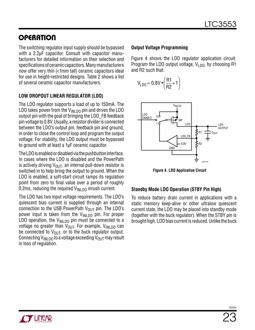
operaTionOutput Voltage Programming
Figure 4 shows the LDO regulator application circuit. Program the LDO output voltage, VLDO, by choosing R1 and R2 such that:
VLDO = 0.8V • R1
R2+ 1
Standby Mode LDO Operation (STBY Pin High)
To reduce battery drain current in applications with a static memory keep-alive or other ultralow quiescent current state, the LDO may be placed into standby mode (together with the buck regulator). When the STBY pin is brought high, LDO bias current is reduced. Unlike the buck
COUT
LDOOUTPUT
LDO_FB
LDOMP
0.8V R2GND
R1
0
1
3553 F04
LDOENABLE
VINLDO
Figure 4. LDO Application Circuit
LTC3553
243553fc
operaTionregulator, the LDO’s load capability remains unchanged. However, the LDO’s transient response is slowed, as il-lustrated in Figure 5 and Figure 6.
measures should be taken to ensure that the buck is not operated outside the specified BVIN input supply range, as operation beyond this range is not guaranteed.
LDO Regulator UVLO Considerations
The LDO regulator’s bias current is supplied via an internal connection to the USB PowerPath VOUT pin. The VOUT UVLO shuts down the LDO when VOUT drops below about 2.6V in order to prevent the LDO from operating incorrectly due to too low a bias supply voltage.
The LDO power input pin, VINLDO, can be driven with as little as 1.65V. There is, however, no UVLO to enforce this requirement. It is thus recommended that VINLDO be tied to either the buck regulator output (programmed to regulate at least 1.65V), or to the USB PowerPath VOUT pin, to ensure proper operation.
PUSHBUTTON INTERFACE
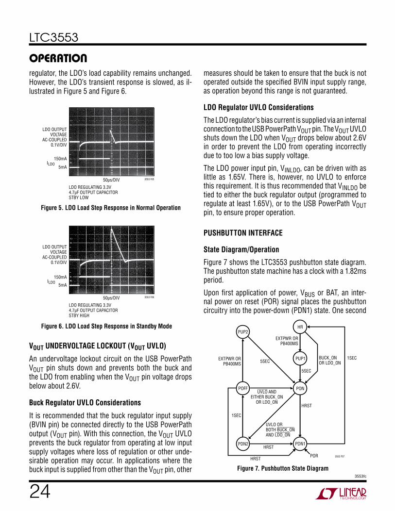
State Diagram/Operation
Figure 7 shows the LTC3553 pushbutton state diagram. The pushbutton state machine has a clock with a 1.82ms period.
Upon first application of power, VBUS or BAT, an inter-nal power on reset (POR) signal places the pushbutton circuitry into the power-down (PDN1) state. One second
Figure 7. Pushbutton State Diagram
3553 F07
PUP2
PDN1PDN2HRST
HRST
HRST
POR
UVLO ANDEITHER BUCK_ON
OR LDO_ON
BUCK_ONOR LDO_ON
EXTPWR ORPB400MS
1SEC
5SEC
5SEC
1SEC
PON
PUP1
HR
UVLO ORBOTH BUCK_ONAND LDO_ON
EXTPWR ORPB400MS
POFF
Figure 5. LDO Load Step Response in Normal Operation
LDO REGULATING 3.3V4.7µF OUTPUT CAPACITORSTBY LOW
LDO OUTPUTVOLTAGE
AC-COUPLED0.1V/DIV
150mA
5mAILDO
3553 F0550µs/DIV
LDO REGULATING 3.3V4.7µF OUTPUT CAPACITORSTBY HIGH
LDO OUTPUTVOLTAGE
AC-COUPLED0.1V/DIV
150mA
5mA
3553 F0650µs/DIV
ILDO
VOUT UNDERVOLTAGE LOCKOUT (VOUT UVLO)
An undervoltage lockout circuit on the USB PowerPath VOUT pin shuts down and prevents both the buck and the LDO from enabling when the VOUT pin voltage drops below about 2.6V.
Buck Regulator UVLO Considerations
It is recommended that the buck regulator input supply (BVIN pin) be connected directly to the USB PowerPath output (VOUT pin). With this connection, the VOUT UVLO prevents the buck regulator from operating at low input supply voltages where loss of regulation or other unde-sirable operation may occur. In applications where the buck input is supplied from other than the VOUT pin, other
Figure 6. LDO Load Step Response in Standby Mode

LTC3553
253553fc
after entering the PDN1 state the pushbutton circuitry will transition into the hard reset (HR) state.
In the HR state, all supplies are disabled. The PowerPath circuitry is placed in an ultralow quiescent state to minimize battery drain. If no external charging supply is present (VBUS) then the ideal diode is shut down, disconnecting VOUT from BAT to further minimize battery drain. The ultra-low power consumption in the HR state makes it ideal for shipping or long term storage, minimizing battery drain.
The following events cause the state machine to transition out of HR into the power-up (PUP1) state:
ON input low for 400ms (PB400MS)
Application of external power (EXTPWR)
Upon entering the PUP1 state, the pushbutton circuitry will sequence up the buck and LDO regulators. The state of the SEQ pin determines which regulator is enabled before the other. If SEQ is low, the buck regulator is enabled first. If SEQ is high, the LDO regulator is enabled first. The second regulator is enabled once the feedback voltage of the first regulator nears regulation. The SEQ pin must be tied to either VOUT or ground.
The BUCK_ON and LDO_ON inputs are ignored in the PUP1 state. The state machine remains in the PUP1 state for five seconds. During the five seconds, the application’s microprocessor, powered by the regulators, has time to boot and assert BUCK_ON and/or LDO_ON. Five seconds after entering the PUP1 state, the pushbutton circuitry automatically transitions into the power-on (PON) state.
In the PON state, the regulators can be enabled and shut down at any time by the BUCK_ON and LDO_ON pins. A high on BUCK_ON is needed to keep the buck enabled, and a high on LDO_ON is needed to keep the LDO enabled. To remain in the PON state, the application circuit must keep at least one of the BUCK_ON or LDO_ON inputs high, else the state machine enters the power-down (PDN2) state.
When BUCK_ON and LDO_ON are both low, or when VOUT drops to its undervoltage lockout (VOUT UVLO) threshold, the state machine will leave the PON state and enter the power-down (PDN2) state. In the power-down state (PDN2), both regulators are kept disabled regardless of the states
of the BUCK_ON and LDO_ON pins. The state machine remains in the power-down state for one second, before automatically entering the power-off (POFF) state. This one second delay allows all LTC3553 generated supplies time to power down completely before they can be re-enabled.
The same events used to exit the hard reset (HR) state are also used to exit the POFF state and enter the PUP2 state. The PUP2 state operates in the same manner as the PUP1 state previously described.
Both regulators remain powered up during the five second power-up (PUP1 or PUP2) period, regardless of the state of the BUCK_ON and LDO_ON inputs.
In either the HR or POFF states, if either the BUCK_ON or LDO_ON pin is driven high, the pushbutton circuitry directly enters the PON state, without passing through the power-up (PUP1 or PUP2) states. This is because by asserting logic high on the BUCK_ON or LDO_ON pins, the application has already told the LTC3553 exactly which regulator(s) to turn on, so there is no need for an inter-mediate PUP state in which both regulators are enabled for five seconds.
Starting from the HR state, bringing the BUCK_ON and/or LDO_ON pin(s) high enables the PowerPath, if it wasn’t already enabled due to VBUS power being available. This powers up the VOUT pin from VBUS or BAT. When the VOUT voltage rises above the VOUT UVLO threshold, the state machine transitions from the HR state into the PON state, allowing the selected regulator(s) to turn on.
The hard reset (HRST) event is generated by pressing and holding the pushbutton (ON input low) for five seconds. For a valid HRST event to occur the button press must start in the PUP1, PUP2 or PON state, but can end in any state. If a valid HRST event is present in PON, PDN2 or POFF, then the state machine will transition to the PDN1 state and subsequently transition to the HR state one second later.
Debounced Pushbutton Output (PBSTAT)
In the PON, PUP1, and PUP2 states, the PBSTAT open-drain output pin outputs a debounced version of the ON pushbutton signal. ON must be held low for at least 50ms for the pushbutton interface to recognize it and cause
operaTion
LTC3553
263553fc
PBSTAT to go low. PBSTAT goes high impedance when ON goes high, except the logic enforces a minimum pulse width of 50ms on PBSTAT.
In the HR, POFF, PDN1, and PDN2 states, PBSTAT remains high impedance regardless of the state of ON.
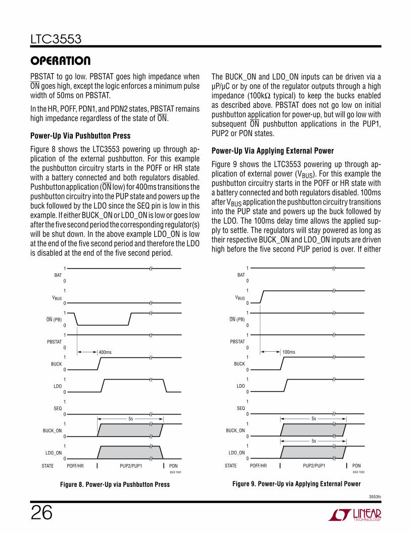
Power-Up Via Pushbutton Press
Figure 8 shows the LTC3553 powering up through ap-plication of the external pushbutton. For this example the pushbutton circuitry starts in the POFF or HR state with a battery connected and both regulators disabled. Pushbutton application (ON low) for 400ms transitions the pushbutton circuitry into the PUP state and powers up the buck followed by the LDO since the SEQ pin is low in this example. If either BUCK_ON or LDO_ON is low or goes low after the five second period the corresponding regulator(s) will be shut down. In the above example LDO_ON is low at the end of the five second period and therefore the LDO is disabled at the end of the five second period.
operaTionThe BUCK_ON and LDO_ON inputs can be driven via a μP/μC or by one of the regulator outputs through a high impedance (100kΩ typical) to keep the bucks enabled as described above. PBSTAT does not go low on initial pushbutton application for power-up, but will go low with subsequent ON pushbutton applications in the PUP1, PUP2 or PON states.
Power-Up Via Applying External Power
Figure 9 shows the LTC3553 powering up through ap-plication of external power (VBUS). For this example the pushbutton circuitry starts in the POFF or HR state with a battery connected and both regulators disabled. 100ms after VBUS application the pushbutton circuitry transitions into the PUP state and powers up the buck followed by the LDO. The 100ms delay time allows the applied sup-ply to settle. The regulators will stay powered as long as their respective BUCK_ON and LDO_ON inputs are driven high before the five second PUP period is over. If either
BAT
VBUS
ON (PB)
PBSTAT
BUCK
LDO
SEQ
BUCK_ON
LDO_ON
STATE POFF/HR PONPUP2/PUP13553 TD02
5s
5s
100ms
1
0
1
0
1
0
1
0
1
0
1
0
1
0
1
0
1
0
Figure 9. Power-Up via Applying External Power
BAT1
0
1
0
1
0
1
0
1
0
1
0
1
0
1
0
1
0
VBUS
ON (PB)
PBSTAT
BUCK
LDO
SEQ
BUCK_ON
LDO_ON
STATE POFF/HR PONPUP2/PUP13553 TD01
5s
400ms
Figure 8. Power-Up via Pushbutton Press
LTC3553
273553fc
operaTionBUCK_ON or LDO_ON is low or goes low after the five second period the corresponding regulator(s) will be shut down. In the above example both pins are high at the end of the five second period and therefore both regulators continue to stay on at the end of the five second period.
The BUCK_ON and LDO_ON inputs can be driven via a μP/μC or one of the regulator outputs through a high impedance (100kΩ typ) to keep the regulators enabled as described above.
Without a battery present, initial power application causes a power-on reset which puts the pushbutton circuitry in the PDN1 state and subsequently the HR state one second later. At this time, if a valid supply voltage is detected at the BUS pin (i.e., VBUS > VUVLO and VBUS – VBAT > VDUVLO), the pushbutton circuity immediately enters the PUP1 state. For this to work reliably, the BAT pin voltage must be kept well-behaved when no battery is connected. Ensure this
by bypassing the BAT pin to GND with an RC network con-sisting of a 100µF ceramic capacitor in series with 0.3Ω.
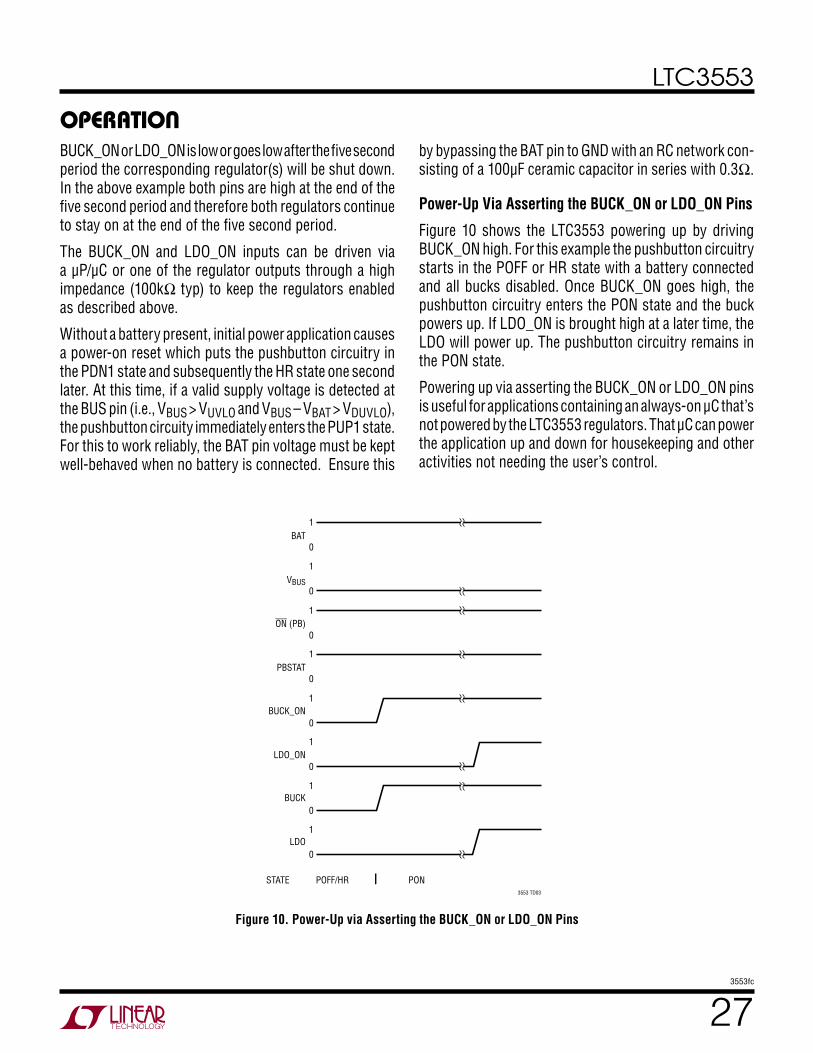
Power-Up Via Asserting the BUCK_ON or LDO_ON Pins
Figure 10 shows the LTC3553 powering up by driving BUCK_ON high. For this example the pushbutton circuitry starts in the POFF or HR state with a battery connected and all bucks disabled. Once BUCK_ON goes high, the pushbutton circuitry enters the PON state and the buck powers up. If LDO_ON is brought high at a later time, the LDO will power up. The pushbutton circuitry remains in the PON state.
Powering up via asserting the BUCK_ON or LDO_ON pins is useful for applications containing an always-on μC that’s not powered by the LTC3553 regulators. That μC can power the application up and down for housekeeping and other activities not needing the user’s control.
BAT
VBUS
ON (PB)
PBSTAT
BUCK
LDO
BUCK_ON
LDO_ON
STATE POFF/HR PON3553 TD03
1
0
1
0
1
0
1
0
1
0
1
0
1
0
1
0
Figure 10. Power-Up via Asserting the BUCK_ON or LDO_ON Pins
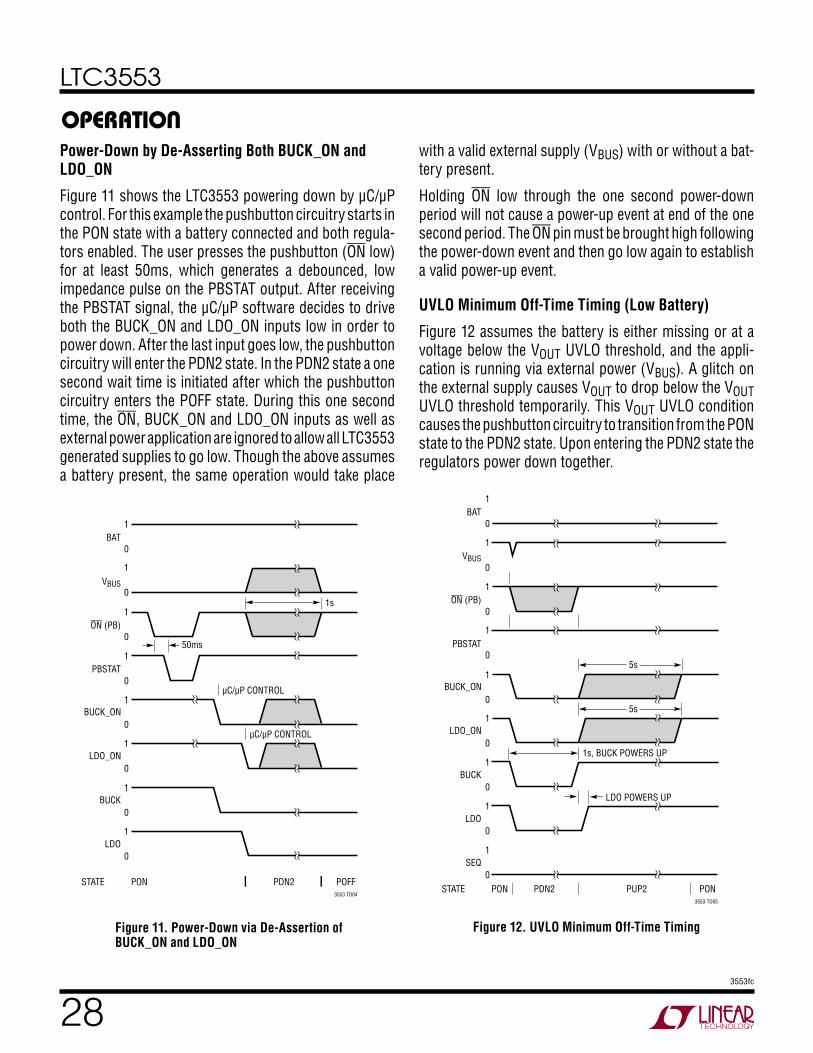
LTC3553
283553fc
Power-Down by De-Asserting Both BUCK_ON and LDO_ON
Figure 11 shows the LTC3553 powering down by μC/μP control. For this example the pushbutton circuitry starts in the PON state with a battery connected and both regula-tors enabled. The user presses the pushbutton (ON low) for at least 50ms, which generates a debounced, low impedance pulse on the PBSTAT output. After receiving the PBSTAT signal, the μC/μP software decides to drive both the BUCK_ON and LDO_ON inputs low in order to power down. After the last input goes low, the pushbutton circuitry will enter the PDN2 state. In the PDN2 state a one second wait time is initiated after which the pushbutton circuitry enters the POFF state. During this one second time, the ON, BUCK_ON and LDO_ON inputs as well as external power application are ignored to allow all LTC3553 generated supplies to go low. Though the above assumes a battery present, the same operation would take place
operaTionwith a valid external supply (VBUS) with or without a bat-tery present.
Holding ON low through the one second power-down period will not cause a power-up event at end of the one second period. The ON pin must be brought high following the power-down event and then go low again to establish a valid power-up event.
UVLO Minimum Off-Time Timing (Low Battery)
Figure 12 assumes the battery is either missing or at a voltage below the VOUT UVLO threshold, and the appli-cation is running via external power (VBUS). A glitch on the external supply causes VOUT to drop below the VOUT UVLO threshold temporarily. This VOUT UVLO condition causes the pushbutton circuitry to transition from the PON state to the PDN2 state. Upon entering the PDN2 state the regulators power down together.
BAT
VBUS
ON (PB)
PBSTAT
BUCK
LDO
SEQ
BUCK_ON
LDO_ON
STATE PON PONPUP2PDN23553 TD05
5s
5s
1s, BUCK POWERS UP
LDO POWERS UP
1
0
1
0
1
0
1
0
1
0
1
0
1
0
1
0
1
0
Figure 12. UVLO Minimum Off-Time Timing
BAT
VBUS
ON (PB)
PBSTAT
BUCK
LDO
BUCK_ON
LDO_ON
STATE PON POFFPDN23553 TD04
1s
µC/µP CONTROL
50ms
µC/µP CONTROL
1
0
1
0
1
0
1
0
1
0
1
0
1
0
1
0
Figure 11. Power-Down via De-Assertion of BUCK_ON and LDO_ON

LTC3553
293553fc
operaTionIn the typical case where the BUCK_ON and LDO_ON pins are driven by logic powered by the regulators, the BUCK_ON and LDO_ON pins would also go low, as depicted in Figure 12. If the external supply recovers after entering the PDN2 state such that VOUT is no longer in UVLO, then the LTC3553 will transition back into the PUP2 state once the PDN2 one second delay is complete. Following the state diagram, the transition from PDN2 to PUP2 in this case actually occurs via a brief visit to the POFF state. During the brief POFF state, the state machine immedi-ately recognizes that valid external power is available and transitions into the PUP2 state. Entering the PUP2 state will cause the buck and LDO to sequence up as described previously in the power-up sections.
Not depicted here, but in cases where the BUCK_ON or LDO_ON pin is driven by a supply other than the LDO or buck that remains high when entering the POFF state, then as per the state diagram in Figure 7, the pushbutton circuitry will enter the PON state once VOUT is no lon-ger in UVLO. Upon entering the PON state, the enabled regulator(s) will power up.
Note: If VOUT drops too low (below about 1.9V) the LTC3553 will see this as a POR condition and will enter the PDN1 state rather than the PDN2 state. One second later the part will transition to the HR state. Under these conditions an explicit power-up event (such as a pushbutton press) may be required to bring the LTC3553 out of hard reset.
Hard Reset Timing
HARD RESET provides an ultralow power-down state for shipping or long term storage as well as a way to power down the application in case of a software lockup. In the case of software lockup, the user can hold the pushbutton (ON low) for five seconds and a hard reset event (HRST)
will occur, placing the pushbutton circuitry in the power-down (PDN1) state. At this point the regulators will be shut down. Following a one second power-down period the pushbutton circuitry will enter the hard reset state (HR).
Holding ON low through the one second power-down period will not cause a power-up event at end of the one second period. ON must be brought high following the power-down event and then go low again for 400ms to establish a valid power-up event, as shown in Figure 13.
BAT
VBUS
ON (PB)
PBSTAT
BUCK
LDO
SEQ
BUCK_ON
LDO_ON
STATE PON PUP1HRPDN13553 TD06
400ms
50ms
5s
1s
1
0
1
0
1
0
1
0
1
0
1
0
1
0
1
0
1
0
Figure 13. Hard Reset via Holding ON Low for Five Seconds
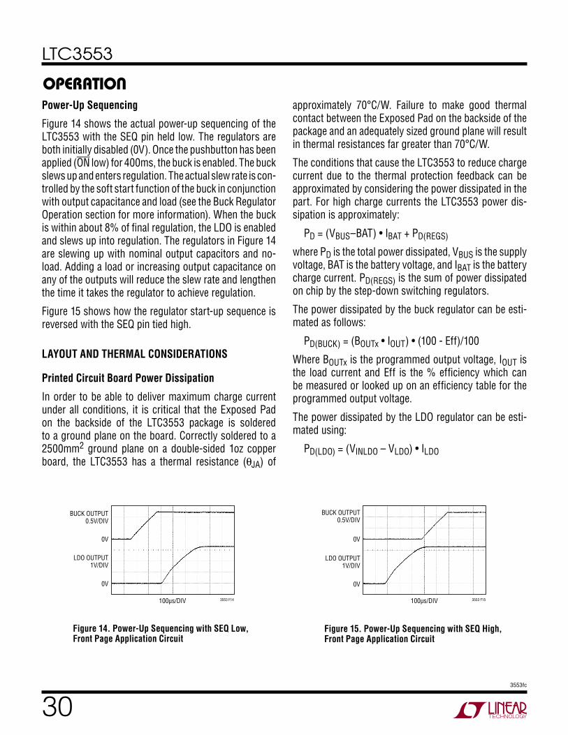
LTC3553
303553fc
Power-Up Sequencing
Figure 14 shows the actual power-up sequencing of the LTC3553 with the SEQ pin held low. The regulators are both initially disabled (0V). Once the pushbutton has been applied (ON low) for 400ms, the buck is enabled. The buck slews up and enters regulation. The actual slew rate is con-trolled by the soft start function of the buck in conjunction with output capacitance and load (see the Buck Regulator Operation section for more information). When the buck is within about 8% of final regulation, the LDO is enabled and slews up into regulation. The regulators in Figure 14 are slewing up with nominal output capacitors and no-load. Adding a load or increasing output capacitance on any of the outputs will reduce the slew rate and lengthen the time it takes the regulator to achieve regulation.
Figure 15 shows how the regulator start-up sequence is reversed with the SEQ pin tied high.
LAYOUT AND THERMAL CONSIDERATIONS
Printed Circuit Board Power Dissipation
In order to be able to deliver maximum charge current under all conditions, it is critical that the Exposed Pad on the backside of the LTC3553 package is soldered to a ground plane on the board. Correctly soldered to a 2500mm2 ground plane on a double-sided 1oz copper board, the LTC3553 has a thermal resistance (θJA) of
approximately 70°C/W. Failure to make good thermal contact between the Exposed Pad on the backside of the package and an adequately sized ground plane will result in thermal resistances far greater than 70°C/W.
The conditions that cause the LTC3553 to reduce charge current due to the thermal protection feedback can be approximated by considering the power dissipated in the part. For high charge currents the LTC3553 power dis-sipation is approximately:
PD = (VBUS–BAT) • IBAT + PD(REGS)
where PD is the total power dissipated, VBUS is the supply voltage, BAT is the battery voltage, and IBAT is the battery charge current. PD(REGS) is the sum of power dissipated on chip by the step-down switching regulators.
The power dissipated by the buck regulator can be esti-mated as follows:
PD(BUCK) = (BOUTx • IOUT) • (100 - Eff)/100
Where BOUTx is the programmed output voltage, IOUT is the load current and Eff is the % efficiency which can be measured or looked up on an efficiency table for the programmed output voltage.
The power dissipated by the LDO regulator can be esti-mated using:
PD(LDO) = (VINLDO – VLDO) • ILDO
operaTion
Figure 14. Power-Up Sequencing with SEQ Low, Front Page Application Circuit
Figure 15. Power-Up Sequencing with SEQ High, Front Page Application Circuit
BUCK OUTPUT0.5V/DIV
LDO OUTPUT1V/DIV
0V
0V
3553 F14100µs/DIV
BUCK OUTPUT0.5V/DIV
LDO OUTPUT1V/DIV
0V
0V
3553 F15100µs/DIV
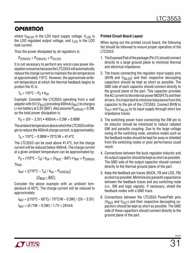
LTC3553
313553fc
where VINLDO is the LDO input supply voltage, VLDO is the LDO regulated output voltage, and ILDO is the LDO load current.
Thus the power dissipated by all regulators is:
PD(REGS) = PD(BUCK) + PD(LDO)
It is not necessary to perform any worst-case power dis-sipation scenarios because the LTC3553 will automatically reduce the charge current to maintain the die temperature at approximately 110°C. However, the approximate ambi-ent temperature at which the thermal feedback begins to protect the IC is:
TA = 110°C – PD • θJA
Example: Consider the LTC3553 operating from a wall adapter with 5V (VBUS) providing 400mA (IBAT) to charge a Li-Ion battery at 3.3V (BAT). Also assume PD(REGS) = 0.3W, so the total power dissipation is:
PD = (5V – 3.3V) • 400mA + 0.3W = 0.98W
The ambient temperature above which the LTC3553 will be-gin to reduce the 400mA charge current, is approximately:
TA = 110°C – 0.98W • 70°C/W = 41.4°C
The LTC3553 can be used above 41.4°C, but the charge current will be reduced below 400mA. The charge current at a given ambient temperature can be approximated by:
PD = (110°C – TA) / θJA = (VBUS – BAT) • IBAT + PD(REGS)
Thus:
IBAT = [(110°C – TA) / θJA – PD(REGS)]
(VBUS – BAT)
Consider the above example with an ambient tem-perature of 60°C. The charge current will be reduced to approximately:
IBAT = [(110°C – 60°C) / 70°C/W – 0.3W] / (5V – 3.3V)
IBAT = (0.71W – 0.3W) / 1.7V = 241mA
Printed Circuit Board Layout
When laying out the printed circuit board, the following list should be followed to ensure proper operation of the LTC3553:
1. The Exposed Pad of the package (Pin 21) should connect directly to a large ground plane to minimize thermal and electrical impedance.
2. The traces connecting the regulator input supply pins (BVIN and VINLDO) and their respective decoupling capacitors should be kept as short as possible. The GND side of each capacitor should connect directly to the ground plane of the part. This capacitor provides the AC current to the internal power MOSFETs and their drivers. It is important to minimize inductance from this capacitor to the pin of the LTC3553. Connect BVIN to VOUT and VINLDO to its input supply through short low impedance traces.
3. The switching power trace connecting the SW pin to its inductor should be minimized to reduce radiated EMI and parasitic coupling. Due to the large voltage swing of the switching node, sensitive nodes such as the feedback nodes should be kept far away or shielded from the switching nodes or poor performance could result.
4. Connections between the buck regulator inductor and its output capacitor should be kept as short as possible. The GND side of the output capacitor should connect directly to the thermal ground plane of the part.
5. Keep the feedback pin traces (BUCK_FB and LDO_FB) as short as possible. Minimize any parasitic capacitance between the feedback traces and any switching node (i.e., SW and logic signals). If necessary, shield the feedback nodes with a GND trace.
6. Connections between the LTC3553 PowerPath pins (VBUS and VOUT) and their respective decoupling ca-pacitors should be kept as short as possible. The GND side of these capacitors should connect directly to the ground plane of the part.
operaTion
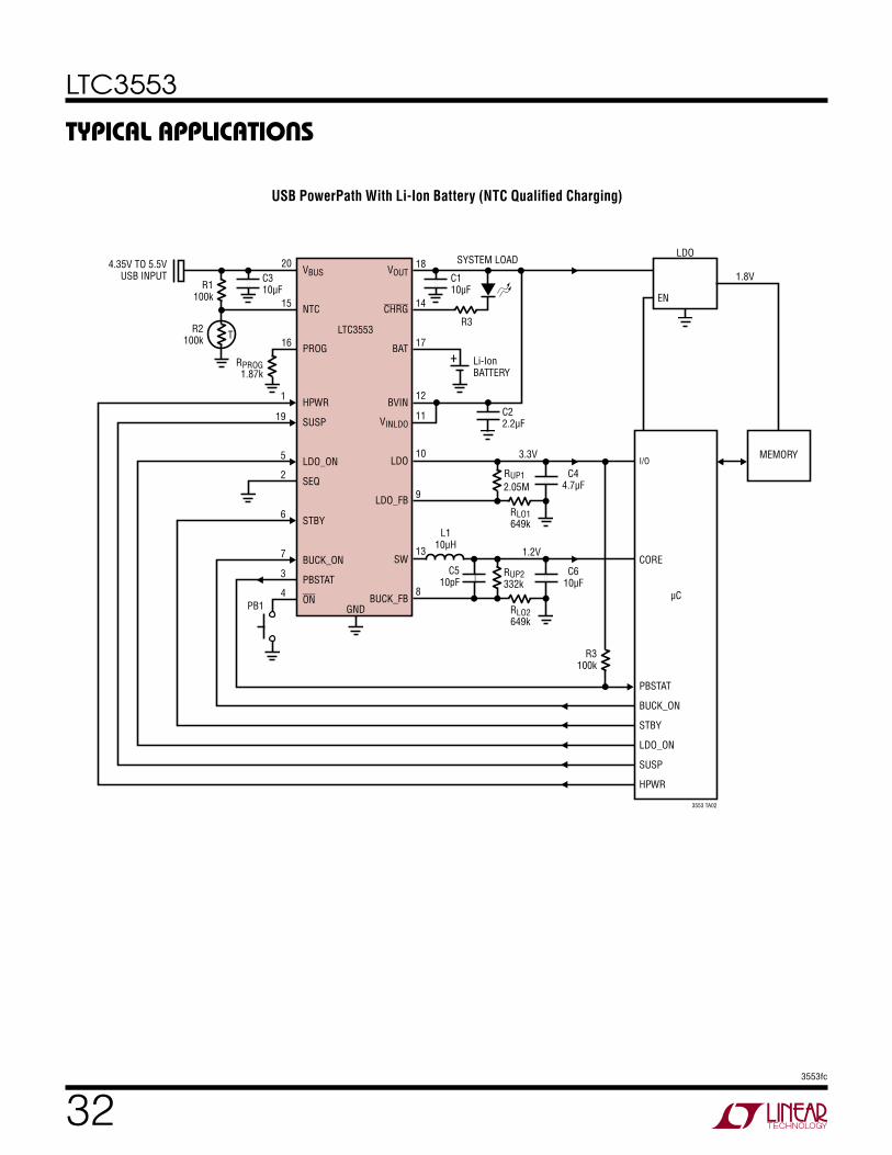
LTC3553
323553fc
Typical applicaTions
VBUS
NTC
PROG
HPWR
SUSP
LDO_ON
SEQ
STBY
BUCK_ON
PBSTAT
ON
VOUT
CHRG
BAT
BVIN
VINLDO
LDO
LDO_FB
SW
BUCK_FBGND
Li-IonBATTERY
C110µF
C310µF
R3
R1100k
20
16
1
19
5
2
6
7
3
4PB1
8
13
9
10
12
11
17
18
1415
RPROG1.87k
T
C44.7µF
C22.2µF
RUP1
RUP2
2.05M
RLO1649k
3.3V
LDO
1.8V
C510pF
C610µF332k
RLO2649k
1.2V
L110µH
SYSTEM LOAD4.35V TO 5.5VUSB INPUT
LTC3553
I/O
CORE
PBSTAT
BUCK_ON
STBY
LDO_ON
SUSP
HPWR
3553 TA02
µC
MEMORY
EN
R2100k
R3100k
+
USB PowerPath With Li-Ion Battery (NTC Qualified Charging)
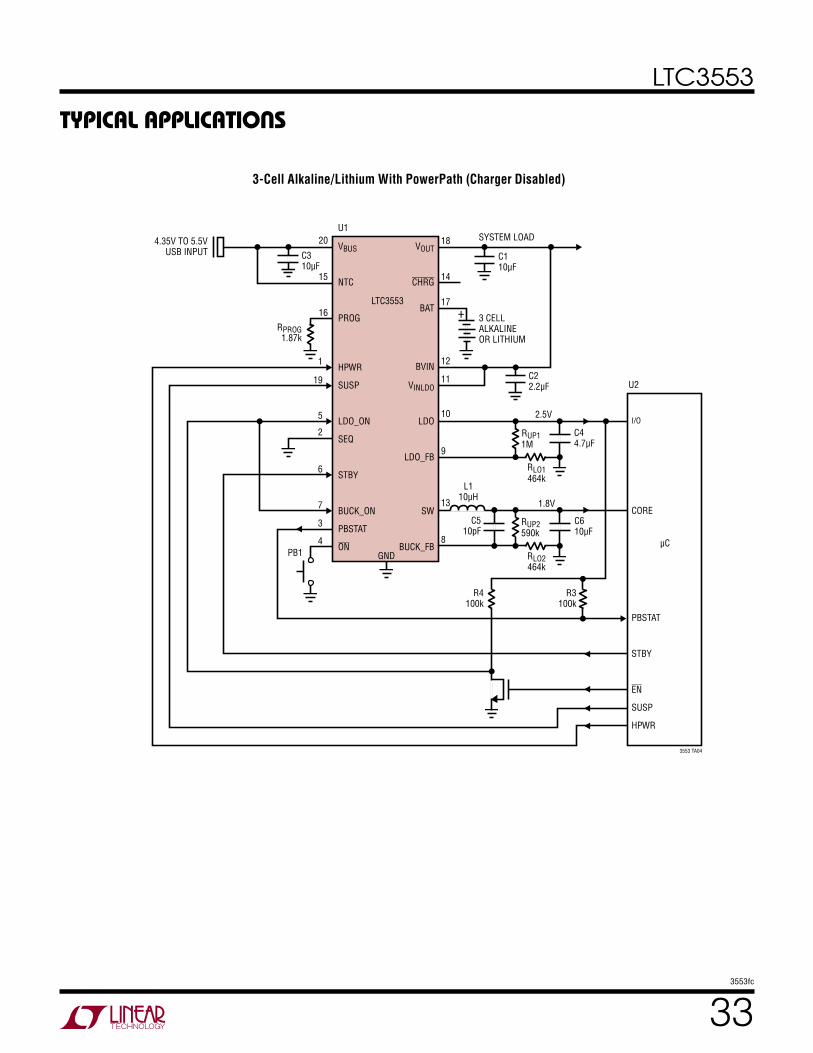
LTC3553
333553fc
Typical applicaTions
VBUS
NTC
PROG
HPWR
SUSP
LDO_ON
SEQ
STBY
BUCK_ON
PBSTAT
ON
VOUT
CHRG
BAT
BVIN
VINLDO
LDO
LDO_FB
SW
BUCK_FBGND
3 CELLALKALINEOR LITHIUM
C110µF
20U1
U2
16
1
19
5
2
6
7
3
4PB1
8
13
9
10
12
11
17
18
1415
RPROG1.87k
C44.7µF
C22.2µF
RUP11M
RUP2590k
RLO1464k
2.5V
C510pF
R4100k
R3100k
C610µF
RLO2464k
1.8V
L110µH
SYSTEM LOAD4.35V TO 5.5VUSB INPUT
LTC3553
I/O
CORE
PBSTAT
STBY
EN
SUSP
HPWR
3553 TA04
µC
+
C310µF
3-Cell Alkaline/Lithium With PowerPath (Charger Disabled)

LTC3553
343553fc
pacKage DescripTion
UD Package20-Lead Plastic QFN (3mm × 3mm)
(Reference LTC DWG # 05-08-1720 Rev A)
3.00 ± 0.10(4 SIDES)
RECOMMENDED SOLDER PAD PITCH AND DIMENSIONSAPPLY SOLDER MASK TO AREAS THAT ARE NOT SOLDERED
1.65 ± 0.05
NOTE:1. DRAWING IS NOT A JEDEC PACKAGE OUTLINE2. DRAWING NOT TO SCALE3. ALL DIMENSIONS ARE IN MILLIMETERS4. DIMENSIONS OF EXPOSED PAD ON BOTTOM OF PACKAGE DO NOT INCLUDE MOLD FLASH. MOLD FLASH, IF PRESENT, SHALL NOT EXCEED 0.15mm ON ANY SIDE5. EXPOSED PAD SHALL BE SOLDER PLATED6. SHADED AREA IS ONLY A REFERENCE FOR PIN 1 LOCATION ON THE TOP AND BOTTOM OF PACKAGE
PIN 1TOP MARK(NOTE 6)
0.40 ± 0.10
BOTTOM VIEW—EXPOSED PAD
1.65 ± 0.10(4-SIDES)
0.75 ± 0.05 R = 0.115TYP
R = 0.05TYP
0.20 ± 0.05
1
PIN 1 NOTCH R = 0.20 TYPOR 0.25 × 45° CHAMFER
19 20
2
0.40 BSC
0.200 REF
2.10 ± 0.05
3.50 ± 0.05(4 SIDES)
0.70 ±0.05
0.00 – 0.05
(UD20) QFN 0306 REV A
0.20 ±0.050.40 BSC
PACKAGEOUTLINE
UD Package20-Lead Plastic QFN (3mm × 3mm)
(Reference LTC DWG # 05-08-1720 Rev A)
Please refer to http://www.linear.com/designtools/packaging/ for the most recent package drawings.
LTC3553
353553fc
Information furnished by Linear Technology Corporation is believed to be accurate and reliable. However, no responsibility is assumed for its use. Linear Technology Corporation makes no representa-tion that the interconnection of its circuits as described herein will not infringe on existing patent rights.
revision hisToryREV DATE DESCRIPTION PAGE NUMBER
A 9/10 PD package information removed and UD package information added to data sheetLTC3553EUD added and LTC3553EPD designated Obsolete in Order Information sectionNote 2 updatedPin 21 description updatedUpdated Related Parts
1 to 16261336
B 1/12 Updated the Block DiagramUpdated State Diagram/Operation section
1424
C 04/15 Changed θJA of package from 70°C/W to 58.7°C/W 2
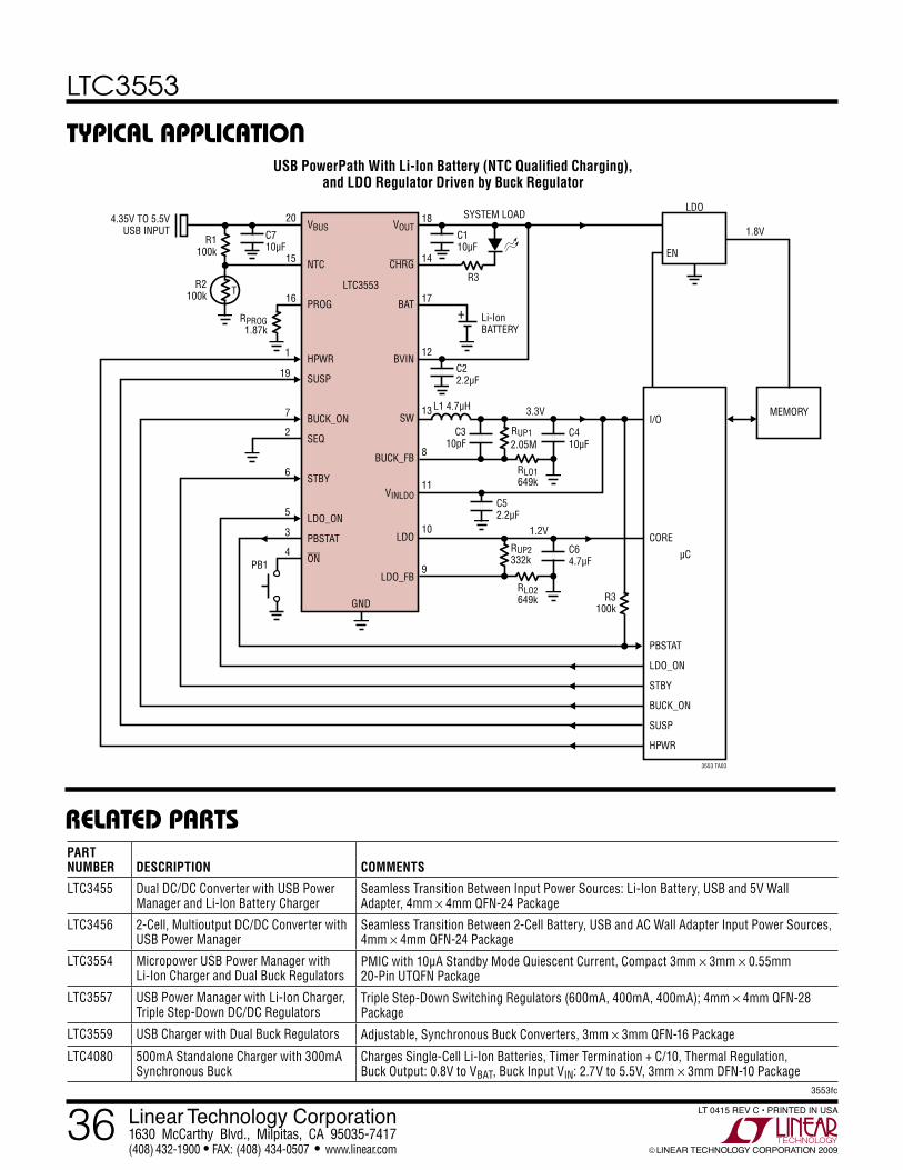
LTC3553
363553fc
Linear Technology Corporation1630 McCarthy Blvd., Milpitas, CA 95035-7417 (408) 432-1900 FAX: (408) 434-0507 www.linear.com LINEAR TECHNOLOGY CORPORATION 2009
LT 0415 REV C • PRINTED IN USA
relaTeD parTsPART NUMBER
DESCRIPTION
COMMENTS
LTC3455 Dual DC/DC Converter with USB Power Manager and Li-Ion Battery Charger
Seamless Transition Between Input Power Sources: Li-Ion Battery, USB and 5V Wall Adapter, 4mm × 4mm QFN-24 Package
LTC3456 2-Cell, Multioutput DC/DC Converter with USB Power Manager
Seamless Transition Between 2-Cell Battery, USB and AC Wall Adapter Input Power Sources, 4mm × 4mm QFN-24 Package
LTC3554 Micropower USB Power Manager with Li-Ion Charger and Dual Buck Regulators
PMIC with 10µA Standby Mode Quiescent Current, Compact 3mm × 3mm × 0.55mm 20-Pin UTQFN Package
LTC3557 USB Power Manager with Li-Ion Charger, Triple Step-Down DC/DC Regulators
Triple Step-Down Switching Regulators (600mA, 400mA, 400mA); 4mm × 4mm QFN-28 Package
LTC3559 USB Charger with Dual Buck Regulators Adjustable, Synchronous Buck Converters, 3mm × 3mm QFN-16 Package
LTC4080 500mA Standalone Charger with 300mA Synchronous Buck
Charges Single-Cell Li-Ion Batteries, Timer Termination + C/10, Thermal Regulation, Buck Output: 0.8V to VBAT, Buck Input VIN: 2.7V to 5.5V, 3mm × 3mm DFN-10 Package
VBUS
NTC
PROG
HPWR
SUSP
BUCK_ON
SEQ
STBY
LDO_ON
PBSTAT
ON
VOUT
CHRG
BAT
BVIN
SW
BUCK_FB
VINLDO
LDO
LDO_FB
GND
Li-IonBATTERY
C110µF
C710µF
R3
R1100k
20
16
1
19
7
2
6
5
3
4PB1 9
10
11
8
13
12
17
18
1415
RPROG1.87k
T
C410µF
C22.2µF
RUP1
RUP2
2.05M
RLO1649k
3.3V
LDO
1.8V
C310pF
C64.7µF332k
RLO2649k
1.2V
C52.2µF
L1 4.7µH
SYSTEM LOAD4.35V TO 5.5VUSB INPUT
LTC3553
I/O
CORE
PBSTAT
LDO_ON
STBY
BUCK_ON
SUSP
HPWR
3553 TA03
µC
MEMORY
EN
R2100k
R3100k
+
USB PowerPath With Li-Ion Battery (NTC Qualified Charging), and LDO Regulator Driven by Buck Regulator
Typical applicaTion