Embed Size (px)
Citation preview
LTC4085
14085fd
USB Power Manager with Ideal Diode Controller and
Li-Ion Charger
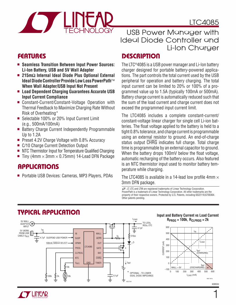
The LTC®4085 is a USB power manager and Li-Ion battery charger designed for portable battery-powered applica-tions. The part controls the total current used by the USB peripheral for operation and battery charging. The total input current can be limited to 20% or 100% of a pro-grammed value up to 1.5A (typically 100mA or 500mA). Battery charge current is automatically reduced such that the sum of the load current and charge current does not exceed the programmed input current limit.
The LTC4085 includes a complete constant-current/constant-voltage linear charger for single cell Li-ion bat-teries. The float voltage applied to the battery is held to a tight 0.8% tolerance, and charge current is programmable using an external resistor to ground. An end-of-charge status output CHRG indicates full charge. Total charge time is programmable by an external capacitor to ground. When the battery drops 100mV below the float voltage, automatic recharging of the battery occurs. Also featured is an NTC thermistor input used to monitor battery tem-perature while charging.
The LTC4085 is available in a 14-lead low profile 4mm × 3mm DFN package.
n Portable USB Devices: Cameras, MP3 Players, PDAs
n Seamless Transition Between Input Power Sources: Li-Ion Battery, USB and 5V Wall Adapter
n 215mΩ Internal Ideal Diode Plus Optional External Ideal Diode Controller Provide Low Loss PowerPath™ When Wall Adapter/USB Input Not Present
n Load Dependent Charging Guarantees Accurate USB Input Current Compliance
n Constant-Current/Constant-Voltage Operation with Thermal Feedback to Maximize Charging Rate Without Risk of Overheating*
n Selectable 100% or 20% Input Current Limit (e.g., 500mA/100mA)n Battery Charge Current Independently Programmable
Up to 1.2An Preset 4.2V Charge Voltage with 0.8% Accuracyn C/10 Charge Current Detection Outputn NTC Thermistor Input for Temperature Qualified Chargingn Tiny (4mm × 3mm × 0.75mm) 14-Lead DFN Package
Input and Battery Current vs Load Current RPROG = 100k, RCLPROG = 2k
L, LT, LTC and LTM are registered trademarks of Linear Technology Corporation. PowerPath is a trademark of Linear Technology Corporation. All other trademarks are the property of their respective owners. Protected by U.S. Patents, including 6522118,6700364. Other patents pending.
IN
SUSP
HPWR
PROG
CLPROG
NTC
VNTC
WALL
ACPR
OUT
GATE
BAT
CHRG
TIMER
LTC4085
GND
+
0.1μF
4.7μF
TO LDOs,REGs, ETC
10k
10k2k100k
4.7μF
5V WALLADAPTER
INPUT
5V (NOM)FROM USB
CABLE VBUSSUSPEND USB POWER
100mA 500mA SELECT
1k 510Ω
4085 TA01
*
* OPTIONAL - TO LOWER IDEAL DIODE IMPEDANCE
IIN
ILOAD
IBAT
ILOAD (mA)
0
600
500
400
300
200
100
0
–100300 500
4085 TA01b
100 200 400 600
CU
RR
EN
T (
mA
) ILOAD
IIN
IBAT(CHARGING)
IBAT(DISCHARGING)WALL = 0V
FEATURES DESCRIPTION
APPLICATIONS
TYPICAL APPLICATION
LTC4085
24085fd
(Notes 1, 2, 3, 4, 5)
Terminal VoltageIN, OUT t < 1ms and Duty Cycle < 1% ................... –0.3V to 7V Steady State ............................................ –0.3V to 6VBAT, CHRG, HPWR, SUSP, WALL, ACPR ..... –0.3V to 6VNTC, TIMER, PROG, CLPROG .......–0.3V to (VCC + 0.3V)
Pin Current (Steady State)IN, OUT, BAT (Note 6) ..............................................2.5AOperating Temperature Range .................–40°C to 85°CMaximum Operating Junction Temperature ...........110°CStorage Temperature Range .................. –65°C to 125°C
The l indicates specifications which apply over the full operating
temperature range, otherwise specifications are at TA = 25°C. VIN = 5V, VBAT = 3.7V, HPWR = 5V, WALL = 0V, RPROG = 100k,RCLPROG = 2k, unless otherwise noted.
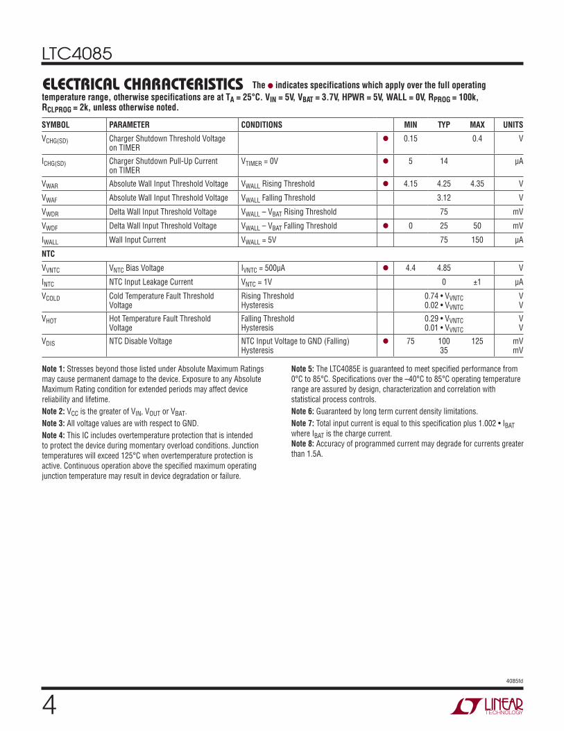
SYMBOL PARAMETER CONDITIONS MIN TYP MAX UNITS
VIN Input Supply Voltage IN and OUT 4.35 5.5 V
VBAT Input Voltage BAT 4.3 V
IIN Input Supply Current IBAT = 0 (Note 7)Suspend Mode; SUSP = 5VSuspend Mode; SUSP = 5V, WALL = 5V,VOUT = 4.8V
l
l
l
0.55060
1.2100110
mAμAμA
IOUT Output Supply Current VOUT = 5V, VIN = 0V, NTC = VNTC l 0.7 1.4 mA
IBAT Battery Drain Current VBAT = 4.3V, Charging StoppedSuspend Mode; SUSP = 5VVIN = 0V, BAT Powers OUT, No Load
l
l
l
152260
2735
100
μAμAμA
VUVLO Input or Output Undervoltage Lockout VIN Powers Part, Rising ThresholdVOUT Powers Part, Rising Threshold
l
l
3.62.75
3.82.95
43.15
VV
∆VUVLO Input or Output Undervoltage Lockout VIN Rising – VIN Fallingor VOUT Rising – VOUT Falling
130 mV
Current Limit
ILIM Current Limit RCLPROG = 2k (0.1%), HPWR = 5VRCLPROG = 2k (0.1%), HPWR = 0V
l
l
47590
500100
525110
mAmA
IIN(MAX) Maximum Input Current Limit (Note 8) 2.4 A
RON ON Resistance VIN to VOUT IOUT = 100mA Load 215 mΩ
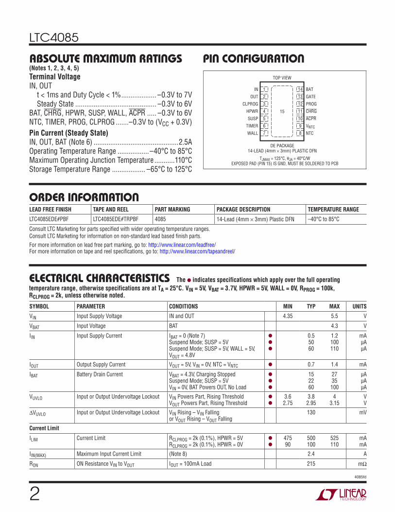
PIN CONFIGURATION
1
2
3
4
5
6
7
14
13
12
11
10
9
8
BAT
GATE
PROG
CHRG
ACPR
VNTC
NTC
IN
OUT
CLPROG
HPWR
SUSP
TIMER
WALL
TOP VIEW
15
DE PACKAGE14-LEAD (4mm 3mm) PLASTIC DFN
TJMAX = 125°C, θJA = 40°C/WEXPOSED PAD (PIN 15) IS GND, MUST BE SOLDERED TO PCB
LEAD FREE FINISH TAPE AND REEL PART MARKING PACKAGE DESCRIPTION TEMPERATURE RANGE
LTC4085EDE#PBF LTC4085EDE#TRPBF 4085 14-Lead (4mm × 3mm) Plastic DFN –40°C to 85°C
Consult LTC Marketing for parts specified with wider operating temperature ranges.
Consult LTC Marketing for information on non-standard lead based finish parts.
For more information on lead free part marking, go to: http://www.linear.com/leadfree/ For more information on tape and reel specifications, go to: http://www.linear.com/tapeandreel/
ABSOLUTE MAXIMUM RATINGS
ORDER INFORMATION
ELECTRICAL CHARACTERISTICS
LTC4085
34085fd
SYMBOL PARAMETER CONDITIONS MIN TYP MAX UNITS
VCLPROG CLPROG Pin Voltage RPROG = 2k
RPROG = 1k
l
l
0.980.98
11
1.021.02
VV
ISS Soft-Start Inrush Current IN or OUT 5 mA/μs
VCLEN Input Current Limit Enable ThresholdVoltage
(VIN – VOUT) VIN Rising
(VIN – VOUT) VIN Falling
20–80
50–60
80–20
mVmV
Battery Charger
VFLOAT Regulated Output Voltage IBAT = 2mA
IBAT = 2mA, (0°C to 85°C)
4.1654.158
4.24.2
4.2354.242
VV
IBAT Current Mode Charge Current RPROG = 100k (0.1%), No Load
RPROG = 50k (0.1%), No Load
l
l
465900
5001000
5351080
mAmA
IBAT(MAX) Maximum Charge Current (Note 8) 1.5 A
VPROG PROG Pin Voltage RPROG = 100k
RPROG = 50k
l
l
0.980.98
11
1.021.02
VV
kEOC Ratio of End-of-Charge Current toCharge Current
VBAT = VFLOAT (4.2V) l 0.085 0.1 0.11 mA/mA
ITRIKL Trickle Charge Current VBAT = 2V, RPROG = 100k (0.1%) 40 50 60 mA
VTRIKL Trickle Charge Threshold Voltage l 2.8 2.9 3 V
VCEN Charger Enable Threshold Voltage (VOUT – VBAT) Falling; VBAT = 4V
(VOUT – VBAT) Rising; VBAT = 4V
5580
mVmV
VRECHRG Recharge Battery Threshold Voltage VFLOAT – VRECHRG l 65 100 135 mV
tTIMER TIMER Accuracy VBAT = 4.3V -10 10 %
Recharge Time Percent of Total Charge Time 50 %
Low-Battery Trickle Charge Time Percent of Total Charge Time, VBAT < 2.8V 25 %
TLIM Junction Temperature in ConstantTemperature Mode
105 °C
Internal Ideal Diode
RFWD Incremental Resistance, VON Regulation IBAT = 100mA 125 mΩ
RDIO(ON) ON Resistance VBAT to VOUT IBAT = 600mA 215 mΩ
VFWD Voltage Forward Drop (VBAT – VOUT) IBAT = 5mA
IBAT = 100mA
IBAT = 600mA
l 10 3055
160
50 mVmVmV
VOFF Diode Disable Battery Voltage 2.8 V
IFWD Load Current Limit, for VON Regulation 550 mA
ID(MAX) Diode Current Limit 2.2 A
External Ideal Diode
VFWD,EDA External Ideal Diode Forward Voltage VGATE = 1.85V; IGATE = 0 20 mV
Logic
VOL Output Low Voltage, CHRG, ACPR ISINK = 5mA l 0.1 0.25 V
VIH Input High Voltage SUSP, HPWR Pin l 1.2 V
VIL Input Low Voltage SUSP, HPWR Pin l 0.4 V
IPULLDN Logic Input Pull-Down Current SUSP, HPWR 2 μA
The l indicates specifications which apply over the full operating
temperature range, otherwise specifications are at TA = 25°C. VIN = 5V, VBAT = 3.7V, HPWR = 5V, WALL = 0V, RPROG = 100k,RCLPROG = 2k, unless otherwise noted.
ELECTRICAL CHARACTERISTICS
LTC4085
44085fd
SYMBOL PARAMETER CONDITIONS MIN TYP MAX UNITS
VCHG(SD) Charger Shutdown Threshold Voltageon TIMER
l 0.15 0.4 V
ICHG(SD) Charger Shutdown Pull-Up Currenton TIMER
VTIMER = 0V l 5 14 μA
VWAR Absolute Wall Input Threshold Voltage VWALL Rising Threshold l 4.15 4.25 4.35 V
VWAF Absolute Wall Input Threshold Voltage VWALL Falling Threshold 3.12 V
VWDR Delta Wall Input Threshold Voltage VWALL – VBAT Rising Threshold 75 mV
VWDF Delta Wall Input Threshold Voltage VWALL – VBAT Falling Threshold l 0 25 50 mV
IWALL Wall Input Current VWALL = 5V 75 150 μA
NTC
VVNTC VNTC Bias Voltage IVNTC = 500μA l 4.4 4.85 V
INTC NTC Input Leakage Current VNTC = 1V 0 ±1 μA
VCOLD Cold Temperature Fault ThresholdVoltage
Rising ThresholdHysteresis
0.74 • VVNTC0.02 • VVNTC
VV
VHOT Hot Temperature Fault ThresholdVoltage
Falling ThresholdHysteresis
0.29 • VVNTC0.01 • VVNTC
VV
VDIS NTC Disable Voltage NTC Input Voltage to GND (Falling)Hysteresis
l 75 10035
125 mVmV
Note 1: Stresses beyond those listed under Absolute Maximum Ratings
may cause permanent damage to the device. Exposure to any Absolute
Maximum Rating condition for extended periods may affect device
reliability and lifetime.
Note 2: VCC is the greater of VIN, VOUT or VBAT.
Note 3: All voltage values are with respect to GND.
Note 4: This IC includes overtemperature protection that is intended
to protect the device during momentary overload conditions. Junction
temperatures will exceed 125°C when overtemperature protection is
active. Continuous operation above the specified maximum operating
junction temperature may result in device degradation or failure.
Note 5: The LTC4085E is guaranteed to meet specified performance from
0°C to 85°C. Specifications over the –40°C to 85°C operating temperature
range are assured by design, characterization and correlation with
statistical process controls.
Note 6: Guaranteed by long term current density limitations.
Note 7: Total input current is equal to this specification plus 1.002 • IBAT
where IBAT is the charge current.
Note 8: Accuracy of programmed current may degrade for currents greater
than 1.5A.
The l indicates specifications which apply over the full operating
temperature range, otherwise specifications are at TA = 25°C. VIN = 5V, VBAT = 3.7V, HPWR = 5V, WALL = 0V, RPROG = 100k,RCLPROG = 2k, unless otherwise noted.
ELECTRICAL CHARACTERISTICS
LTC4085
54085fd
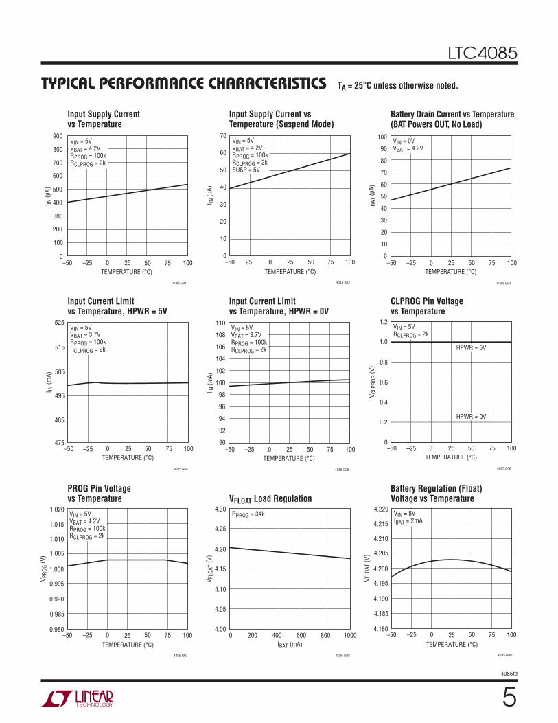
Input Supply Current vs Temperature
Input Supply Current vs Temperature (Suspend Mode)
Battery Drain Current vs Temperature (BAT Powers OUT, No Load)
Input Current Limit vs Temperature, HPWR = 5V
Input Current Limit vs Temperature, HPWR = 0V
CLPROG Pin Voltage vs Temperature
PROG Pin Voltage vs Temperature VFLOAT Load Regulation
Battery Regulation (Float) Voltage vs Temperature
TA = 25°C unless otherwise noted.TYPICAL PERFORMANCE CHARACTERISTICS
TEMPERATURE (°C)
–500
I IN
(μA
)
100
300
400
500
50
900
4085 G01
200
0–25 7525 100
600
700
800
VIN = 5VVBAT = 4.2VRPROG = 100kRCLPROG = 2k
TEMPERATURE (°C)
–50
70
60
50
40
30
20
10
025 75
4085 G02
25 0 50 100
I IN
(μA
)
VIN = 5VVBAT = 4.2VRPROG = 100kRCLPROG = 2kSUSP = 5V
TEMPERATURE (°C)
–500
I BA
T (
μA
)
20
40
60
–25 0 25 50
4085 G03
75
80
100
10
30
50
70
90
100
VIN = 0VVBAT = 4.2V
TEMPERATURE (°C)
–50475
I IN
(m
A)
485
495
505
515
525
–25 0 25 50
4085 G04
75 100
VIN = 5VVBAT = 3.7VRPROG = 100kRCLPROG = 2k
TEMPERATURE (°C)
–50
I IN
(m
A)
92
96
100
–25 0 25 50
4085 G05
75
104
108
110
90
94
98
102
106
100
VIN = 5VVBAT = 3.7VRPROG = 100kRCLPROG = 2k
TEMPERATURE (°C)
–500
VC
LP
RO
G (
V)
0.2
0.4
0.6
0.8
1.2
–25 0 25 50
4085 G06
75 100
1.0
VIN = 5VRCLPROG = 2k
HPWR = 5V
HPWR = 0V
TEMPERATURE (°C)
–50
VP
RO
G (
V)
0.995
1.000
1.005
25 75
4085 G07
0.990
0.985
0.980–25 0 50
1.010
1.015
1.020
100
VIN = 5VVBAT = 4.2VRPROG = 100kRCLPROG = 2k
IBAT (mA)
04.00
VFL
OA
T (
V)
4.05
4.10
4.15
4.20
4.25
4.30
200 400 600 800
4085 G08
1000
RPROG = 34k
TEMPERATURE (°C)
–50
VFL
OA
T (
V)
4.195
4.200
4.205
25 75
4085 G09
4.190
4.185
4.180–25 0 50
4.210
4.215
4.220
100
VIN = 5VIBAT = 2mA
LTC4085
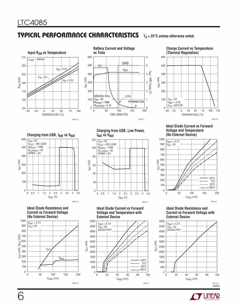
64085fd
Input RON vs TemperatureBattery Current and Voltage vs Time
Charge Current vs Temperature (Thermal Regulation)
Charging from USB, IBAT vs VBAT
Charging from USB, Low Power, IBAT vs VBAT
Ideal Diode Current vs Forward Voltage and Temperature (No External Device)
Ideal Diode Resistance and Current vs Forward Voltage (No External Device)
Ideal Diode Current vs Forward Voltage and Temperature with External Device
Ideal Diode Resistance and Current vs Forward Voltage with External Device
TA = 25°C unless otherwise noted.TYPICAL PERFORMANCE CHARACTERISTICS
TEMPERATURE (°C)
–50125
RO
N (
mΩ
)
150
175
200
225
275
–25 0 25 50
4085 G10
75 100
250
VIN = 4.5V
VIN = 5.5V
ILOAD = 400mA
VIN = 5V
TIME (MINUTES)
00
I BA
T (
mA
)
100
200
300
400
500
600
0
VB
AT A
ND
VC
HR
G (V
)
1
2
3
4
5
6
50 100 150 200
4085 G11
400mAhr CELLVIN = 5VRPROG = 100kRCLPROG = 2.1k
C/10
CHRG
VBAT
IBAT
TERMINATION
TEMPERATURE (°C)
–50
I BA
T (
mA
)
400
500
600
25 75
4085 G12
300
200
–25 0 50 100 125
100
0
VIN = 5VVBAT = 3.5V
JA = 50°C/W
VBAT (V)
00
I BA
T (
mA
)
100
300
400
500
1 2 2.5 4.5
4085 G13
200
0.5 1.5 3 3.5 4
600VIN = 5VVOUT = NO LOADRPROG = 100kRCLPROG = 2kHPWR = 5V
VBAT (V)
00
I BA
T (
mA
)
20
60
80
100
1 2 2.5 4.5
4085 G14
40
0.5 1.5 3 3.5 4
120VIN = 5VVOUT = NO LOADRPROG = 100kRCLPROG = 2kHPWR = 0V
VFWD (mV)
00
I OU
T (
mA
)
100
300
400
500
1000
700
50 100
4085 G15
200
800
900
600
150 200
VBAT = 3.7VVIN = 0V
–50°C0°C
50°C100°C
VFWD (mV)
00
I OU
T (
mA
), R
DIO
(m
Ω)
100
300
400
500
1000
700
50 100
4085 G16
200
800
900
600
150 200
VBAT = 3.7VVIN = 0V
RDIO
IOUT
0
3000
4000
5000
80
4085 G17
2000
1000
2500
3500
4500
1500
500
020 40 60 100
VFWD (mV)
I OU
T (
mA
)
VBAT = 3.7VVIN = 0VSi2333 PFET
–50°C0°C
50°C100°C
0
3000
4000
5000
80
4085 G18
2000
1000
2500
3500
4500
1500
500
020 40 60 100
VFWD (mV)
I OU
T (
mA
)
VBAT = 3.7VVIN = 0VSi2333 PFET
LTC4085
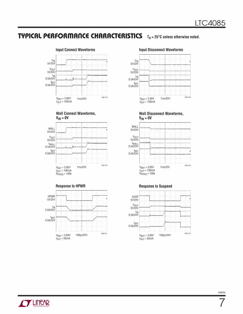
74085fd
Input Connect Waveforms
Input Disconnect Waveforms
Response to HPWR
Wall Connect Waveforms,VIN = 0V
Wall Disconnect Waveforms,VIN = 0V
Response to Suspend
TA = 25°C unless otherwise noted.TYPICAL PERFORMANCE CHARACTERISTICS
1ms/DIV
VIN5V/DIV
VOUT5V/DIV
IIN0.5A/DIV
IBAT0.5A/DIV
4085 G19VBAT = 3.85VIOUT = 100mA
1ms/DIV
VIN5V/DIV
VOUT5V/DIV
IIN0.5A/DIV
IBAT0.5A/DIV
4085 G20VBAT = 3.85VIOUT = 100mA
1ms/DIV
WALL5V/DIV
VOUT5V/DIV
IWALL0.5A/DIV
IBAT0.5A/DIV
4085 G22
VBAT = 3.85VIOUT = 100mARPROG = 100k
1ms/DIV
WALL5V/DIV
VOUT5V/DIV
IWALL0.5A/DIV
IBAT0.5A/DIV
4085 G23
VBAT = 3.85VIOUT = 100mARPROG = 100k
100μs/DIV
HPWR5V/DIV
IIN0.5A/DIV
IBAT0.5A/DIV
4085 G21
VBAT = 3.85VIOUT = 50mA
100μs/DIV
SUSP5V/DIV
VOUT5V/DIV
IIN0.5A/DIV
IBAT0.5A/DIV
4085 G24
VBAT = 3.85VIOUT = 50mA
LTC4085
84085fd
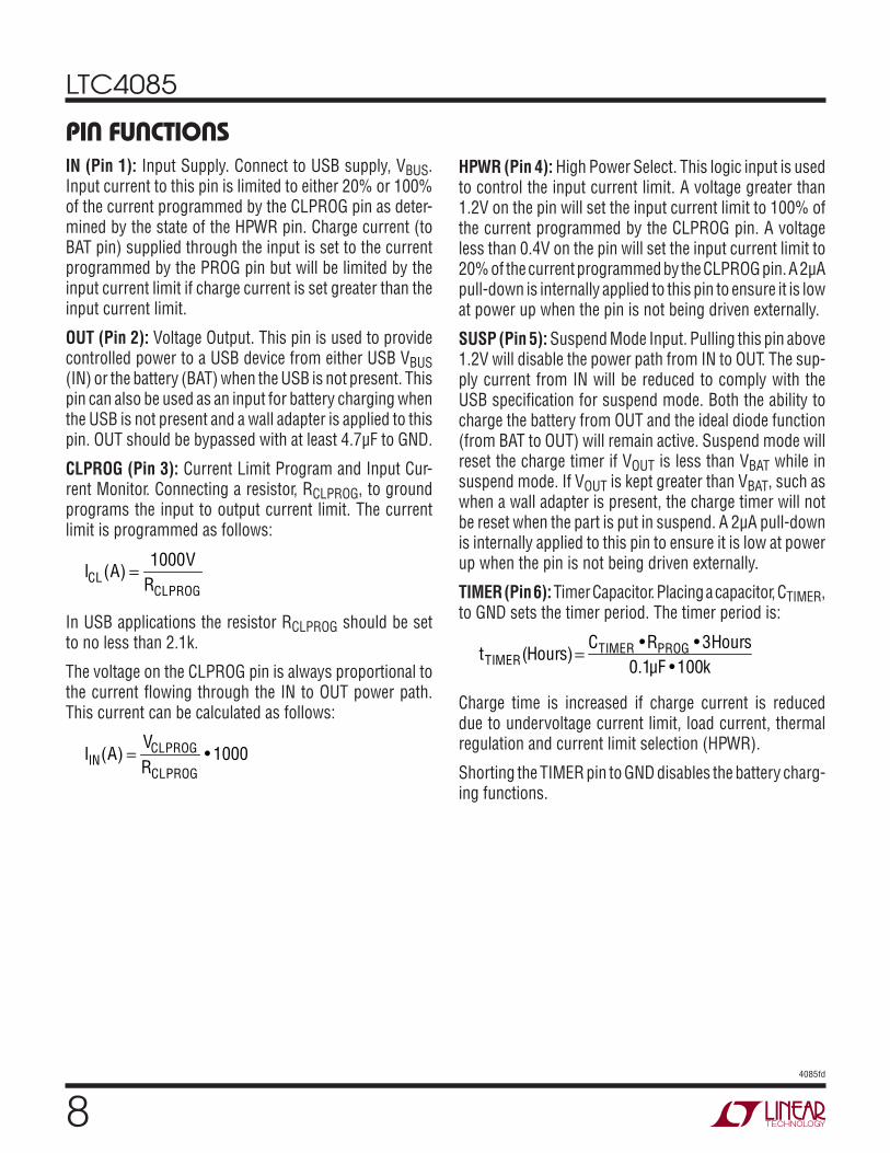
IN (Pin 1): Input Supply. Connect to USB supply, VBUS. Input current to this pin is limited to either 20% or 100% of the current programmed by the CLPROG pin as deter-mined by the state of the HPWR pin. Charge current (to BAT pin) supplied through the input is set to the current programmed by the PROG pin but will be limited by the input current limit if charge current is set greater than the input current limit.
OUT (Pin 2): Voltage Output. This pin is used to provide controlled power to a USB device from either USB VBUS (IN) or the battery (BAT) when the USB is not present. This pin can also be used as an input for battery charging when the USB is not present and a wall adapter is applied to this pin. OUT should be bypassed with at least 4.7μF to GND.
CLPROG (Pin 3): Current Limit Program and Input Cur-rent Monitor. Connecting a resistor, RCLPROG, to ground programs the input to output current limit. The current limit is programmed as follows:
ICL(A) =
1000VRCLPROG
In USB applications the resistor RCLPROG should be set to no less than 2.1k.
The voltage on the CLPROG pin is always proportional to the current flowing through the IN to OUT power path. This current can be calculated as follows:
IIN(A) =
VCLPROG
RCLPROG• 1000
HPWR (Pin 4): High Power Select. This logic input is used to control the input current limit. A voltage greater than 1.2V on the pin will set the input current limit to 100% of the current programmed by the CLPROG pin. A voltage less than 0.4V on the pin will set the input current limit to 20% of the current programmed by the CLPROG pin. A 2μA pull-down is internally applied to this pin to ensure it is low at power up when the pin is not being driven externally.
SUSP (Pin 5): Suspend Mode Input. Pulling this pin above 1.2V will disable the power path from IN to OUT. The sup-ply current from IN will be reduced to comply with the USB specification for suspend mode. Both the ability to charge the battery from OUT and the ideal diode function (from BAT to OUT) will remain active. Suspend mode will reset the charge timer if VOUT is less than VBAT while in suspend mode. If VOUT is kept greater than VBAT, such as when a wall adapter is present, the charge timer will not be reset when the part is put in suspend. A 2μA pull-down is internally applied to this pin to ensure it is low at power up when the pin is not being driven externally.
TIMER (Pin 6): Timer Capacitor. Placing a capacitor, CTIMER, to GND sets the timer period. The timer period is:
tTIMER(Hours)=
CTIMER •RPROG • 3Hours0.1μF •100k
Charge time is increased if charge current is reduced due to undervoltage current limit, load current, thermal regulation and current limit selection (HPWR).
Shorting the TIMER pin to GND disables the battery charg-ing functions.
PIN FUNCTIONS
LTC4085
94085fd
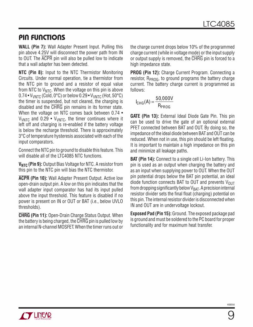
WALL (Pin 7): Wall Adapter Present Input. Pulling this pin above 4.25V will disconnect the power path from IN to OUT. The ACPR pin will also be pulled low to indicate that a wall adapter has been detected.
NTC (Pin 8): Input to the NTC Thermistor Monitoring Circuits. Under normal operation, tie a thermistor from the NTC pin to ground and a resistor of equal value from NTC to VNTC. When the voltage on this pin is above0.74 • VVNTC (Cold, 0°C) or below 0.29 • VVNTC (Hot, 50°C) the timer is suspended, but not cleared, the charging is disabled and the CHRG pin remains in its former state. When the voltage on NTC comes back between 0.74 • VVNTC and 0.29 • VVNTC, the timer continues where it left off and charging is re-enabled if the battery voltage is below the recharge threshold. There is approximately 3°C of temperature hysteresis associated with each of the input comparators.
Connect the NTC pin to ground to disable this feature. This will disable all of the LTC4085 NTC functions.
VNTC (Pin 9): Output Bias Voltage for NTC. A resistor from this pin to the NTC pin will bias the NTC thermistor.
ACPR (Pin 10): Wall Adapter Present Output. Active low open-drain output pin. A low on this pin indicates that the wall adapter input comparator has had its input pulled above the input threshold. This feature is disabled if no power is present on IN or OUT or BAT (i.e., below UVLO thresholds).
CHRG (Pin 11): Open-Drain Charge Status Output. When the battery is being charged, the CHRG pin is pulled low by an internal N-channel MOSFET. When the timer runs out or
the charge current drops below 10% of the programmed charge current (while in voltage mode) or the input supply or output supply is removed, the CHRG pin is forced to a high impedance state.
PROG (Pin 12): Charge Current Program. Connecting a resistor, RPROG, to ground programs the battery charge current. The battery charge current is programmed as follows:
ICHG(A) =
50,000VRPROG
GATE (Pin 13): External Ideal Diode Gate Pin. This pin can be used to drive the gate of an optional external PFET connected between BAT and OUT. By doing so, the impedance of the ideal diode between BAT and OUT can be reduced. When not in use, this pin should be left floating. It is important to maintain a high impedance on this pin and minimize all leakage paths.
BAT (Pin 14): Connect to a single cell Li-Ion battery. This pin is used as an output when charging the battery and as an input when supplying power to OUT. When the OUT pin potential drops below the BAT pin potential, an ideal diode function connects BAT to OUT and prevents VOUT from dropping significantly below VBAT. A precision internal resistor divider sets the final float (charging) potential on this pin. The internal resistor divider is disconnected when IN and OUT are in undervoltage lockout.
Exposed Pad (Pin 15): Ground. The exposed package pad is ground and must be soldered to the PC board for proper functionality and for maximum heat transfer.
PIN FUNCTIONS
LTC4085
104085fd
BLOCK DIAGRAM
+–
–
+
+
–
+
–
+
–
+
–
+
–
+
–
+
–
+
–
+
–
+–
CC/CV REGULATORCHARGER
ENABLE
ENABLE
CURRENT LIMIT
ILIM_CNTL
VBUS
IN
SOFT_START
SOFT_START2
CURRENT_CONTROL
0.25V
2.8VBATTERY UVLO
4.1VRECHARGE
TIMEROSCILLATOR
COUNTERSTOP
CHRG
EOC
CONTROL_LOGIC
RESET
HOLD
RECHRG
BAT_UV
VOLTAGE_DETECT
IN OUT BAT
CHARGE_CONTROL
100k
100k
NTC_ENABLE
2C0LD
2HOT
NTC
NTCERR
GND SUSP
+
–
+–
100k
2k
OUT
GATE
BAT
EDA
IDEAL_DIODE
25mV
25mV
CLK
C/10
ILIMCL
1V1000
500mA/100mA
2μA
CLPROG
HPWR
TA
DIE TEMP 105°C
1VCHG
PROG
+–25mV
ACPR4.25V
WALL
VNTC
NTC
0.1V
2μA
4085 BD
3
4
1
12
7
10
9
811
6
2
13
14
ICHRG
UVLO
IIN
LTC4085
114085fd
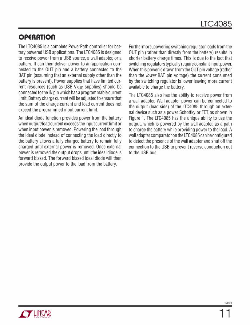
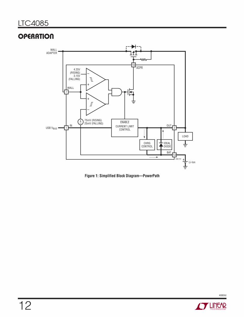
The LTC4085 is a complete PowerPath controller for bat-tery powered USB applications. The LTC4085 is designed to receive power from a USB source, a wall adapter, or a battery. It can then deliver power to an application con-nected to the OUT pin and a battery connected to the BAT pin (assuming that an external supply other than the battery is present). Power supplies that have limited cur-rent resources (such as USB VBUS supplies) should be connected to the IN pin which has a programmable current limit. Battery charge current will be adjusted to ensure that the sum of the charge current and load current does not exceed the programmed input current limit.
An ideal diode function provides power from the battery when output/load current exceeds the input current limit or when input power is removed. Powering the load through the ideal diode instead of connecting the load directly to the battery allows a fully charged battery to remain fully charged until external power is removed. Once external power is removed the output drops until the ideal diode is forward biased. The forward biased ideal diode will then provide the output power to the load from the battery.
Furthermore, powering switching regulator loads from the OUT pin (rather than directly from the battery) results in shorter battery charge times. This is due to the fact that switching regulators typically require constant input power. When this power is drawn from the OUT pin voltage (rather than the lower BAT pin voltage) the current consumed by the switching regulator is lower leaving more current available to charge the battery.
The LTC4085 also has the ability to receive power from a wall adapter. Wall adapter power can be connected to the output (load side) of the LTC4085 through an exter-nal device such as a power Schottky or FET, as shown in Figure 1. The LTC4085 has the unique ability to use the output, which is powered by the wall adapter, as a path to charge the battery while providing power to the load. A wall adapter comparator on the LTC4085 can be configured to detect the presence of the wall adapter and shut off the connection to the USB to prevent reverse conduction out to the USB bus.
OPERATION
LTC4085
124085fd
Figure 1: Simplified Block Diagram—PowerPath
OPERATION
–
+
–
+
7
WALL
4.25V(RISING)
3.15V(FALLING)
75mV (RISING)25mV (FALLING)
1 2
10
14
INUSB VBUS
WALLADAPTER
OUT
BAT
4085 F01
CURRENT LIMITCONTROL
ENABLE
CHRGCONTROL
IDEALDIODE
Li-Ion
LOAD
+–
ACPR
+
LTC4085
134085fd
WALL PRESENT SUSPEND VIN > 3.8V VIN > (VOUT + 100mV) VIN > (VBAT + 100mV) CURRENT LIMIT ENABLED
Y X X X X N
X Y X X X N
X X N X X N
X X X N X N
X X X X N N
N N Y Y Y Y
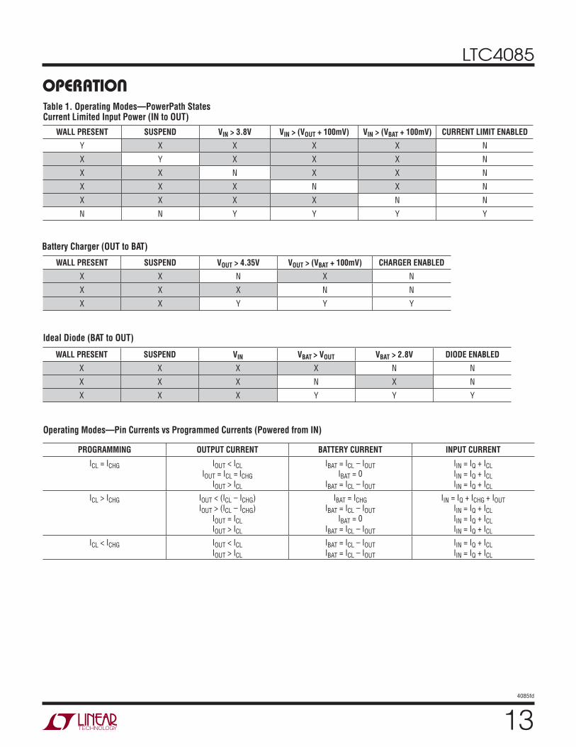
Table 1. Operating Modes—PowerPath StatesCurrent Limited Input Power (IN to OUT)
Battery Charger (OUT to BAT)
WALL PRESENT SUSPEND VOUT > 4.35V VOUT > (VBAT + 100mV) CHARGER ENABLED
X X N X N
X X X N N
X X Y Y Y
Ideal Diode (BAT to OUT)
WALL PRESENT SUSPEND VIN VBAT > VOUT VBAT > 2.8V DIODE ENABLED
X X X X N N
X X X N X N
X X X Y Y Y
Operating Modes—Pin Currents vs Programmed Currents (Powered from IN)
PROGRAMMING OUTPUT CURRENT BATTERY CURRENT INPUT CURRENT
ICL = ICHG IOUT < ICL
IOUT = ICL = ICHG
IOUT > ICL
IBAT = ICL – IOUT
IBAT = 0
IBAT = ICL – IOUT
IIN = IQ + ICL
IIN = IQ + ICL
IIN = IQ + ICL
ICL > ICHG IOUT < (ICL – ICHG)
IOUT > (ICL – ICHG)
IOUT = ICL
IOUT > ICL
IBAT = ICHG
IBAT = ICL – IOUT
IBAT = 0
IBAT = ICL – IOUT
IIN = IQ + ICHG + IOUT
IIN = IQ + ICL
IIN = IQ + ICL
IIN = IQ + ICL
ICL < ICHG IOUT < ICL
IOUT > ICL
IBAT = ICL – IOUT
IBAT = ICL – IOUT
IIN = IQ + ICL
IIN = IQ + ICL
OPERATION
LTC4085
144085fd
USB Current Limit and Charge Current Control
The current limit and charger control circuits of the LTC4085 are designed to limit input current as well as control battery charge current as a function of IOUT. The programmed current limit, ICL, is defined as:
ICL =
1000RCLPROG
• VCLPROG⎛
⎝⎜⎞
⎠⎟=
1000VRCLPROG
The programmed battery charge current, ICHG, is defined as:
ICHG = 50,000
RPROG• VPROG
⎛⎝⎜
⎞⎠⎟
= 50,000VRPROG
Input current, IIN, is equal to the sum of the BAT pin output current and the OUT pin output current:
IIN = IOUT + IBAT
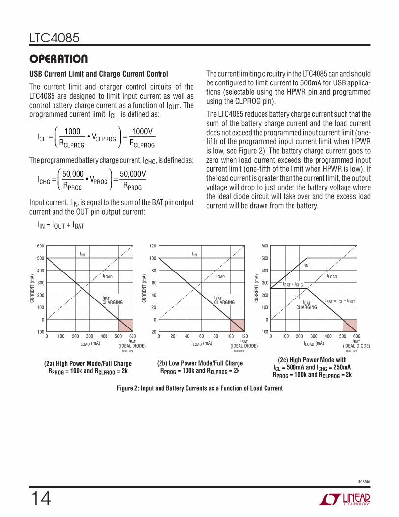
The current limiting circuitry in the LTC4085 can and should be configured to limit current to 500mA for USB applica-tions (selectable using the HPWR pin and programmed using the CLPROG pin).
The LTC4085 reduces battery charge current such that the sum of the battery charge current and the load current does not exceed the programmed input current limit (one-fifth of the programmed input current limit when HPWR is low, see Figure 2). The battery charge current goes to zero when load current exceeds the programmed input current limit (one-fifth of the limit when HPWR is low). If the load current is greater than the current limit, the output voltage will drop to just under the battery voltage where the ideal diode circuit will take over and the excess load current will be drawn from the battery.
(2a) High Power Mode/Full ChargeRPROG = 100k and RCLPROG = 2k
(2b) Low Power Mode/Full ChargeRPROG = 100k and RCLPROG = 2k
(2c) High Power Mode withICL = 500mA and ICHG = 250mARPROG = 100k and RCLPROG = 2k
Figure 2: Input and Battery Currents as a Function of Load Current
OPERATION
ILOAD (mA)
0
CU
RR
EN
T (
mA
)
300
400
600
500IIN
400
4085 F02a
200
100
–100
0
100 200 300 600500
ILOAD
IBATCHARGING
IBAT(IDEAL DIODE)
ILOAD (mA)
0
CU
RR
EN
T (
mA
)
300
400
600
500
IIN
400
4085 F02c
200
100
–100
0
100 200 300 600500
ILOAD
IBATCHARGING
IBAT(IDEAL DIODE)
IBAT = ICHG
IBAT = ICL – IOUT
ILOAD (mA)
0
CU
RR
EN
T (
mA
)
60
80
120
100IIN
80
4085 F02b
40
20
–20
0
20 40 60 120100
ILOAD
IBATCHARGING
IBAT(IDEAL DIODE)
LTC4085
154085fd
Programming Current Limit
The formula for input current limit is:
ICL =
1000RCLPROG
• VCLPROG⎛
⎝⎜⎞
⎠⎟=
1000VRCLPROG
where VCLPROG is the CLPROG pin voltage and RCLPROG is the total resistance from the CLPROG pin to ground.
For example, if typical 500mA current limit is required, calculate:
RCLPROG =
1V500mA
• 1000 = 2k
In USB applications, the minimum value for RCLPROG should be 2.1k. This will prevent the application current from exceeding 500mA due to LTC4085 tolerances and quiescent currents. A 2.1k CLPROG resistor will give a typical current limit of 476mA in high power mode(HPWR = 1) or 95mA in low power mode (HPWR = 0).
VCLPROG will track the input current according to the fol-lowing equation:
IIN =
VCLPROG
RCLPROG• 1000
For best stability over temperature and time, 1% metal film resistors are recommended.
Ideal Diode from BAT to OUT
The LTC4085 has an internal ideal diode as well as a con-troller for an optional external ideal diode. If a battery is the only power supply available or if the load current exceeds the programmed input current limit, then the battery will automatically deliver power to the load via an ideal diode circuit between the BAT and OUT pins. The ideal diode circuit (along with the recommended 4.7μF capacitor on the OUT pin) allows the LTC4085 to handle large transient loads and wall adapter or USB VBUS connect/disconnect scenarios without the need for large bulk capacitors. The ideal diode responds within a few microseconds and pre-
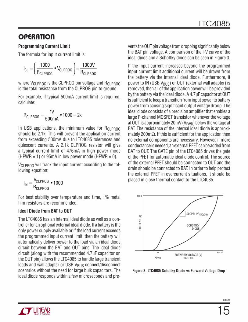
vents the OUT pin voltage from dropping significantly below the BAT pin voltage. A comparison of the I-V curve of the ideal diode and a Schottky diode can be seen in Figure 3.
If the input current increases beyond the programmed input current limit additional current will be drawn from the battery via the internal ideal diode. Furthermore, if power to IN (USB VBUS) or OUT (external wall adapter) is removed, then all of the application power will be provided by the battery via the ideal diode. A 4.7μF capacitor at OUT is sufficient to keep a transition from input power to battery power from causing significant output voltage droop. The ideal diode consists of a precision amplifier that enables a large P-channel MOSFET transistor whenever the voltage at OUT is approximately 20mV (VFWD) below the voltage at BAT. The resistance of the internal ideal diode is approxi-mately 200mΩ. If this is sufficient for the application then no external components are necessary. However, if more conductance is needed, an external PFET can be added from BAT to OUT. The GATE pin of the LTC4085 drives the gate of the PFET for automatic ideal diode control. The source of the external PFET should be connected to OUT and the drain should be connected to BAT. In order to help protect the external PFET in overcurrent situations, it should be placed in close thermal contact to the LTC4085.
FORWARD VOLTAGE (V)(BAT-OUT)
CU
RR
EN
T (
A)
SCHOTTKYDIODE
SLOPE: 1/RDIO(ON)
IMAX
VFWD
4085 F03
Figure 3. LTC4085 Schottky Diode vs Forward Voltage Drop
OPERATION
LTC4085
164085fd
Battery Charger
The battery charger circuits of the LTC4085 are designed for charging single cell lithium-ion batteries. Featuring an internal P-channel power MOSFET, the charger uses a constant-current/constant-voltage charge algorithm with programmable current and a programmable timer for charge termination. Charge current can be programmed up to 1.5A. The final float voltage accuracy is ±0.8% typi-cal. No blocking diode or sense resistor is required when powering the IN pin. The CHRG open-drain status output provides information regarding the charging status of the LTC4085 at all times. An NTC input provides the option of charge qualification using battery temperature.
An internal thermal limit reduces the programmed charge current if the die temperature attempts to rise above a preset value of approximately 105°C. This feature protects the LTC4085 from excessive temperature, and allows the user to push the limits of the power handling capability of a given circuit board without risk of damaging the LTC4085. Another benefit of the LTC4085 thermal limit is that charge current can be set according to typical, not worst-case, ambient temperatures for a given application with the assurance that the charger will automatically reduce the current in worst-case conditions.
The charge cycle begins when the voltage at the OUT pin rises above the output UVLO level and the battery volt-age is below the recharge threshold. No charge current actually flows until the OUT voltage is greater than the output UVLO level and 100mV above the BAT voltage. At the beginning of the charge cycle, if the battery voltage is below 2.8V, the charger goes into trickle charge mode to bring the cell voltage up to a safe level for charging. The charger goes into the fast charge constant-current mode once the voltage on the BAT pin rises above 2.8V.
In constant-current mode, the charge current is set by RPROG. When the battery approaches the final float voltage, the charge current begins to decrease as the LTC4085 switches to constant-voltage mode. When the charge current drops below 10% of the programmed charge current while in constant-voltage mode the CHRG pin assumes a high impedance state.
An external capacitor on the TIMER pin sets the total minimum charge time. When this time elapses the charge cycle terminates and the CHRG pin assumes a high impedance state, if it has not already done so. While charging in constant-current mode, if the charge current is decreased by thermal regulation or in order to maintain the programmed input current limit the charge time is automatically increased. In other words, the charge time is extended inversely proportional to charge current de-livered to the battery. For Li-Ion and similar batteries that require accurate final float potential, the internal bandgap reference, voltage amplifier and the resistor divider provide regulation with ±0.8% accuracy.
Trickle Charge and Defective Battery Detection
At the beginning of a charge cycle, if the battery voltage is low (below 2.8V) the charger goes into trickle charge reducing the charge current to 10% of the full-scale cur-rent. If the low-battery voltage persists for one quarter of the total charge time, the battery is assumed to be defective, the charge cycle is terminated and the CHRG pin output assumes a high impedance state. If for any reason the battery voltage rises above ~2.8V the charge cycle will be restarted. To restart the charge cycle (i.e. when the dead battery is replaced with a discharged battery), simply remove the input voltage and reapply it or cycle the TIMER pin to 0V.
OPERATION
LTC4085
174085fd
Programming Charge Current
The formula for the battery charge current is:
ICHG = IPROG( ) • 50,000 =
VPROGRPROG
• 50,000
where VPROG is the PROG pin voltage and RPROG is the total resistance from the PROG pin to ground. Keep in mind that when the LTC4085 is powered from the IN pin, the programmed input current limit takes precedent over the charge current. In such a scenario, the charge current cannot exceed the programmed input current limit.
For example, if typical 500mA charge current is required, calculate:
RPROG = 1V
500mA⎛⎝⎜
⎞⎠⎟
• 50,000 = 100k
For best stability over temperature and time, 1% metal film resistors are recommended. Under trickle charge condi-tions, this current is reduced to 10% of the full-scale value.
The Charge Timer
The programmable charge timer is used to terminate the charge cycle. The timer duration is programmed by an external capacitor at the TIMER pin. The charge time is typically:
tTIMER(Hours)=
CTIMER •RPROG • 3Hours0.1µF •100k
The timer starts when an input voltage greater than the undervoltage lockout threshold level is applied or when leaving shutdown and the voltage on the battery is less than the recharge threshold. At power up or exiting shutdown with the battery voltage less than the recharge threshold the charge time is a full cycle. If the battery is greater than the recharge threshold the timer will not start and charging
is prevented. If after power-up the battery voltage drops below the recharge threshold or if after a charge cycle the battery voltage is still below the recharge threshold the charge time is set to one half of a full cycle.
The LTC4085 has a feature that extends charge time au-tomatically. Charge time is extended if the charge current in constant-current mode is reduced due to load current or thermal regulation. This change in charge time is in-versely proportional to the change in charge current. As the LTC4085 approaches constant-voltage mode the charge current begins to drop. This change in charge current is due to normal charging operation and does not affect the timer duration.
Once a time-out occurs and the voltage on the battery is greater than the recharge threshold, the charge current stops, and the CHRG output assumes a high impedance state if it has not already done so.
Connecting the TIMER pin to ground disables the battery charger.
CHRG Status Output Pin
When the charge cycle starts, the CHRG pin is pulled to ground by an internal N-channel MOSFET capable of driving an LED. When the charge current drops below 10% of the programmed full charge current while in constant-voltage mode, the pin assumes a high impedance state (but charge current continues to flow until the charge time elapses). If this state is not reached before the end of the program-mable charge time, the pin will assume a high impedance state when a time-out occurs. The CHRG current detection threshold can be calculated by the following equation:
IDETECT =
0.1VRPROG
• 50,000 =5000VRPROG
OPERATION
LTC4085
184085fd
For example, if the full charge current is programmed to 500mA with a 100k PROG resistor the CHRG pin will change state at a battery charge current of 50mA.
Note: The end-of-charge (EOC) comparator that moni-tors the charge current latches its decision. Therefore, the first time the charge current drops below 10% of the programmed full charge current while in constant-voltage mode will toggle CHRG to a high impedance state. If, for some reason, the charge current rises back above the threshold the CHRG pin will not resume the strong pull-down state. The EOC latch can be reset by a recharge cycle (i.e. VBAT drops below the recharge threshold) or toggling the input power to the part.
Current Limit Undervoltage Lockout
An internal undervoltage lockout circuit monitors the input voltage and disables the input current limit circuits until VIN rises above the undervoltage lockout threshold. The current limit UVLO circuit has a built-in hysteresis of 125mV. Furthermore, to protect against reverse current in the power MOSFET, the current limit UVLO circuit disables the current limit (i.e. forces the input power path to a high impedance state) if VOUT exceeds VIN. If the current limit UVLO comparator is tripped, the current limit circuits will not come out of shutdown until VOUT falls 50mV below the VIN voltage.
Charger Undervoltage Lockout
An internal undervoltage lockout circuit monitors the VOUT voltage and disables the battery charger circuits until VOUT rises above the undervoltage lockout threshold. The battery charger UVLO circuit has a built-in hysteresis of 125mV. Furthermore, to protect against reverse current in the power MOSFET, the charger UVLO circuit keeps the charger shut down if VBAT exceeds VOUT. If the charger UVLO comparator is tripped, the charger circuits will not come out of shut down until VOUT exceeds VBAT by 50mV.
Suspend
The LTC4085 can be put in suspend mode by forcing the SUSP pin greater than 1V. In suspend mode the ideal diode function from BAT to OUT is kept alive. If power is applied to the OUT pin externally (i.e., a wall adapter is present) then charging will be unaffected. Current drawn from the IN pin is reduced to 50μA. Suspend mode is intended to comply with the USB power specification mode of the same name.
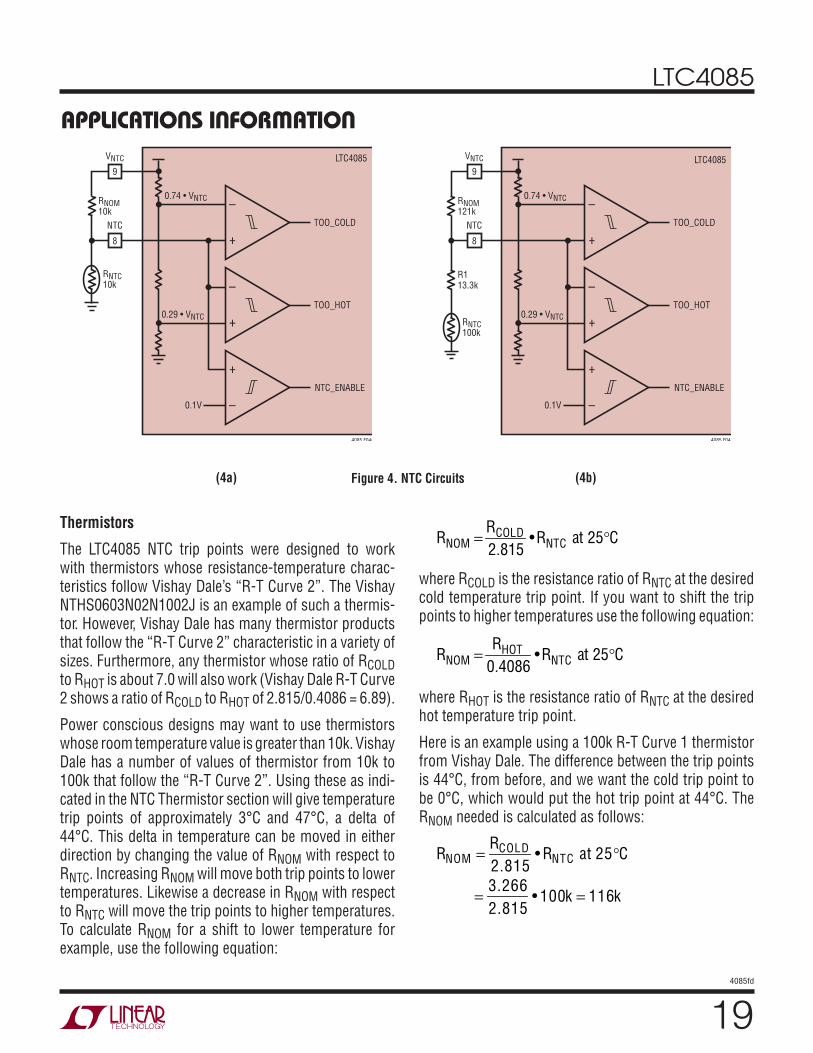
NTC Thermistor
The battery temperature is measured by placing a negative temperature coefficient (NTC) thermistor close to the bat-tery pack. The NTC circuitry is shown in Figure 4. To use this feature, connect the NTC thermistor (RNTC) between the NTC pin and ground and a resistor (RNOM) from the NTC pin to VNTC. RNOM should be a 1% resistor with a value equal to the value of the chosen NTC thermistor at 25°C (this value is 10k for a Vishay NTHS0603N02N1002J thermistor). The LTC4085 goes into hold mode when the resistance (RHOT) of the NTC thermistor drops to 0.41 times the value of RNOM or approximately 4.1k, which should be at 50°C. The hold mode freezes the timer and stops the charge cycle until the thermistor indicates a return to a valid temperature. As the temperature drops, the resistance of the NTC thermistor rises. The LTC4085 is designed to go into hold mode when the value of the NTC thermistor increases to 2.82 times the value of RNOM. This resistance is RCOLD. For a Vishay NTHS0603N02N1002J thermistor, this value is 28.2k which corresponds to ap-proximately 0°C. The hot and cold comparators each have approximately 3°C of hysteresis to prevent oscillation about the trip point. Grounding the NTC pin can disable the NTC function.
OPERATION
LTC4085
194085fd
–
+
–
+
RNOM10k
RNTC10k
NTC
VNTC
9
0.1V
NTC_ENABLE
4085 F04a
LTC4085
TOO_COLD
TOO_HOT
0.74 • VNTC
0.29 • VNTC
–
+8
–
+
–
+
RNOM121k
RNTC100k
R113.3k
NTC
VNTC
9
0.1V
NTC_ENABLE
4085 F04b
TOO_COLD
TOO_HOT
0.74 • VNTC
0.29 • VNTC
–
+8
LTC4085
(4a) (4b)Figure 4. NTC Circuits
Thermistors
The LTC4085 NTC trip points were designed to work with thermistors whose resistance-temperature charac-teristics follow Vishay Dale’s “R-T Curve 2”. The Vishay NTHS0603N02N1002J is an example of such a thermis-tor. However, Vishay Dale has many thermistor products that follow the “R-T Curve 2” characteristic in a variety of sizes. Furthermore, any thermistor whose ratio of RCOLD to RHOT is about 7.0 will also work (Vishay Dale R-T Curve 2 shows a ratio of RCOLD to RHOT of 2.815/0.4086 = 6.89).
Power conscious designs may want to use thermistors whose room temperature value is greater than 10k. Vishay Dale has a number of values of thermistor from 10k to 100k that follow the “R-T Curve 2”. Using these as indi-cated in the NTC Thermistor section will give temperature trip points of approximately 3°C and 47°C, a delta of 44°C. This delta in temperature can be moved in either direction by changing the value of RNOM with respect to RNTC. Increasing RNOM will move both trip points to lower temperatures. Likewise a decrease in RNOM with respect to RNTC will move the trip points to higher temperatures. To calculate RNOM for a shift to lower temperature for example, use the following equation:
RNOM =
RCOLD2.815
•RNTC at 25°C
where RCOLD is the resistance ratio of RNTC at the desired cold temperature trip point. If you want to shift the trip points to higher temperatures use the following equation:
RNOM =
RHOT0.4086
•RNTC at 25°C
where RHOT is the resistance ratio of RNTC at the desired hot temperature trip point.
Here is an example using a 100k R-T Curve 1 thermistor from Vishay Dale. The difference between the trip points is 44°C, from before, and we want the cold trip point to be 0°C, which would put the hot trip point at 44°C. The RNOM needed is calculated as follows:
RNOM =RCOLD
2.815• RNTC at 25°C
=3.2662.815
• 100k = 116k
APPLICATIONS INFORMATION
LTC4085
204085fd
The nearest 1% value for RNOM is 115K. This is the value used to bias the NTC thermistor to get cold and hot trip points of approximately 0°C and 44°C respectively. To extend the delta between the cold and hot trip points a resistor (R1) can be added in series with RNTC. (see Figure 3b). The values of the resistors are calculated as follows:
RNOM =RCOLD – RHOT
2.815 – 0.4086
R1=0.4086
2.815 – 0.4086⎛⎝⎜
⎞⎠⎟
• RCOLD – RHOT( ) – RHOT
where RNOM is the value of the bias resistor, RHOT and RCOLD are the values of RNTC at the desired temperature trip points. Continuing the example from before with a desired hot trip point of 50°C:
RNOM =RCOLD – RHOT
2.815 – 0.4086=
100k • 3.266 – 0.3602( )2.815 – 0.4086
= 120.8k, 121k nearest 1%
R1 = 100k •0.4086
2.815 – 0.4086⎛⎝⎜
⎞⎠⎟
• 3.266 – 0.3602( ) – 0.3602⎡
⎣⎢
⎤
⎦⎥
= 13.3k, 13.3k is nearest 1%
The final solution is as shown in Figure 3b whereRNOM = 121k, R1 = 13.3k and RNTC = 100k at 25°C
Using the WALL Pin to Detect the Presence of a Wall Adapter
The WALL input pin identifies the presence of a wall adapter (the pin should be tied directly to the adapter output voltage). This information is used to disconnect the input pin, IN, from the OUT pin in order to prevent back conduction to whatever may be connected to the input. It also forces the ACPR pin low when the voltage at the WALL pin exceeds the input threshold. In order for the presence of a wall adapter to be acknowledged, both of the following conditions must be satisfied:
1. The WALL pin voltage exceeds VWAR (approximately 4.25V); and
2. The WALL pin voltage exceeds VWDR (approximately 75mV above VBAT)
The input power path (between IN and OUT) is re-enabled and the ACPR pin assumes a high impedance state when either of the following conditions is met:
1. The WALL pin voltage falls below VWDF (approximately 25mV above VBAT); or
2. The WALL pin voltage falls below VWAF (approximately 3.12V)
Each of these thresholds is suitably filtered in time to prevent transient glitches on the WALL pin from falsely triggering an event.
Power Dissipation
The conditions that cause the LTC4085 to reduce charge current due to the thermal protection feedback can be approximated by considering the power dissipated in the part. For high charge currents and a wall adapter applied to VOUT, the LTC4085 power dissipation is approximately:
PD = (VOUT – VBAT) • IBAT
Where, PD is the power dissipated, VOUT is the supply voltage, VBAT is the battery voltage, and IBAT is the battery charge current. It is not necessary to perform any worst-case power dissipation scenarios because the LTC4085 will automatically reduce the charge current to maintain the die temperature at approximately 105°C. However, the approximate ambient temperature at which the thermal feedback begins to protect the IC is:
TA = 105°C – PD • θJA
TA = 105°C – (VOUT – VBAT) • IBAT • θJA
Example: Consider an LTC4085 operating from a wall adapter with 5V at VOUT providing 0.8A to a 3V Li-Ion battery. The ambient temperature above which the LTC4085 will begin to reduce the 0.8A charge current, is approximately
TA = 105°C – (5V – 3V) • 0.8A • 37°C/W
TA = 105°C – 1.6W • 37°C/W = 105°C – 59°C = 46°C
The LTC4085 can be used above 46°C, but the charge current will be reduced below 0.8A. The charge current at a given ambient temperature can be approximated by:
IBAT =
105°C – TAVOUT – VBAT( ) • θJA
APPLICATIONS INFORMATION
LTC4085
214085fd
Consider the above example with an ambient temperature of 55°C. The charge current will be reduced to approximately:
IBAT = 105°C – 55°C
5V – 3V( ) • 37°C/W= 50°C
74°C/A= 0.675A
Board Layout Considerations
In order to be able to deliver maximum charge current under all conditions, it is critical that the Exposed Pad on the backside of the LTC4085 package is soldered to the board. Correctly soldered to a 2500mm2 double-sided 1oz. copper board the LTC4085 has a thermal resistance of approximately 37°C/W. Failure to make thermal contact between the Exposed Pad on the backside of the package and the copper board will result in thermal resistances far greater than 37°C/W. As an example, a correctly soldered LTC4085 can deliver over 1A to a battery from a 5V supply at room temperature. Without a backside thermal connec-tion, this number could drop to less than 500mA.
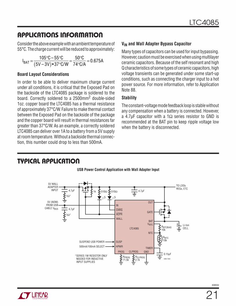
VIN and Wall Adapter Bypass Capacitor
Many types of capacitors can be used for input bypassing. However, caution must be exercised when using multilayer ceramic capacitors. Because of the self resonant and high Q characteristics of some types of ceramic capacitors, high voltage transients can be generated under some start-up conditions, such as connecting the charger input to a hot power source. For more information, refer to Application Note 88.
Stability
The constant-voltage mode feedback loop is stable without any compensation when a battery is connected. However, a 4.7μF capacitor with a 1Ω series resistor to GND is recommended at the BAT pin to keep ripple voltage low when the battery is disconnected.
APPLICATIONS INFORMATION
USB Power Control Application with Wall Adapter Input
IN
SUSP
HPWR
SUSPEND USB POWER
500mA/100mA SELECT
OUT
PROG
LTC4085
CLPROG GND
BAT
GATE
VNTC
NTC
Li-IonCELL
TO LDOsREGs, ETC
CHRG
ACPR
WALL
TIMER
0.15μF
4085 TA02
RNTCBIAS10k
RNTC10k
510Ω
RPROG71.5k
*SERIES 1W RESISTOR ONLY NEEDED FOR INDUCTIVE INPUT SUPPLIES
RCLPROG2.1k
+
4.7μF4.7μF 510Ω1k
5V WALLADAPTER
INPUT
5V (NOM)FROM USB
CABLE VBUS
1Ω*
4.7μF
1Ω*
TYPICAL APPLICATION
LTC4085
224085fd
DE Package14-Lead Plastic DFN (4mm × 3mm)
(Reference LTC DWG # 05-08-1708 Rev B)
3.00 ±0.10(2 SIDES)
4.00 ±0.10(2 SIDES)
NOTE:1. DRAWING PROPOSED TO BE MADE VARIATION OF VERSION (WGED-3) IN JEDEC PACKAGE OUTLINE MO-2292. DRAWING NOT TO SCALE 3. ALL DIMENSIONS ARE IN MILLIMETERS4. DIMENSIONS OF EXPOSED PAD ON BOTTOM OF PACKAGE DO NOT INCLUDE MOLD FLASH. MOLD FLASH, IF PRESENT, SHALL NOT EXCEED 0.15mm ON ANY SIDE5. EXPOSED PAD SHALL BE SOLDER PLATED6. SHADED AREA IS ONLY A REFERENCE FOR PIN 1 LOCATION ON THE TOP AND BOTTOM OF PACKAGE
0.40 ± 0.10
BOTTOM VIEW—EXPOSED PAD
1.70 ± 0.10
0.75 ±0.05
R = 0.115TYP
R = 0.05TYP
3.00 REF
1.70 ± 0.05
17
148
PIN 1TOP MARK
(SEE NOTE 6)
0.200 REF
0.00 – 0.05
(DE14) DFN 0806 REV B
PIN 1 NOTCHR = 0.20 OR0.35 45°CHAMFER
3.00 REF
RECOMMENDED SOLDER PAD PITCH AND DIMENSIONSAPPLY SOLDER MASK TO AREAS THAT ARE NOT SOLDERED
2.20 ±0.05
0.70 ±0.05
3.60 ±0.05
PACKAGEOUTLINE
0.25 ± 0.05
0.25 ± 0.050.50 BSC
3.30 ±0.05
3.30 ±0.10
0.50 BSC
PACKAGE DESCRIPTION
LTC4085
234085fd
Information furnished by Linear Technology Corporation is believed to be accurate and reliable.However, no responsibility is assumed for its use. Linear Technology Corporation makes no represen-tation that the interconnection of its circuits as described herein will not infringe on existing patent rights.
REVISION HISTORYREV DATE DESCRIPTION PAGE NUMBER
D 4/11 Updated Block Diagram 10
(Revision history begins at Rev D)
LTC4085
244085fd
Linear Technology Corporation1630 McCarthy Blvd., Milpitas, CA 95035-7417 (408) 432-1900 ● FAX: (408) 434-0507 ● www.linear.com © LINEAR TECHNOLOGY CORPORATION 2006
LT 0411 REV D • PRINTED IN USA
PART NUMBER DESCRIPTION COMMENTS
Battery Chargers
LTC1733 Monolithic Lithium-Ion Linear Battery Charger Standalone Charger with Programmable Timer, Up to 1.5A Charge Current
LTC1734 Lithium-Ion Linear Battery Charger in ThinSOT™ Simple ThinSOT Charger, No Blocking Diode, No Sense Resistor Needed
LTC1734L Lithium-Ion Linear Battery Charger in ThinSOT Low Current Version of LTC1734; 50mA ≤ ICHRG ≤ 180mA
LTC4002 Switch Mode Lithium-Ion Battery Charger Standalone, 4.7V ≤ VIN ≤ 24 V, 500kHz Frequency, 3 Hour Charge Termination
LTC4052 Monolithic Lithium-Ion Battery Pulse Charger No Blocking Diode or External Power FET Required, ≤ 1.5A Charge Current
LTC4053 USB Compatible Monolithic Li-Ion Battery Charger Standalone Charger with Programmable Timer, Up to 1.25A Charge Current
LTC4054 Standalone Linear Li-Ion Battery Chargerwith Integrated Pass Transistor in ThinSOT
Thermal Regulation Prevents Overheating, C/10 Termination,C/10 Indicator, Up to 800mA Charge Current
LTC4057 Lithium-Ion Linear Battery Charger Up to 800mA Charge Current, Thermal Regulation, ThinSOT Package
LTC4058 Standalone 950mA Lithium-Ion Charger in DFN C/10 Charge Termination, Battery Kelvin Sensing, ±7% Charge Accuracy
LTC4059 900mA Linear Lithium-Ion Battery Charger 2mm × 2mm DFN Package, Thermal Regulation, Charge Current Monitor Output
LTC4065/LTC4065A Standalone Li-Ion Battery Chargers in 2mm × 2mm DFN
4.2V, ±0.6% Float Voltage, Up to 750mA Charge Current, 2mm × 2mm DFN,“A” Version has ACPR Function.
LTC4411/LTC4412 Low Loss PowerPath Controller in ThinSOT Automatic Switching Between DC Sources, Load Sharing,Replaces ORing Diodes
Power Management
LTC3405/LTC3405A 300mA (IOUT), 1.5 MHz, Synchronous Step-DownDC/DC Converter
95% Efficiency, VIN = 2.7V to 6V, VOUT = 0.8V, IQ = 20μA, ISD < 1μA,ThinSOT Package
LTC3406/LTC3406A 600mA (IOUT), 1.5 MHz, Synchronous Step-DownDC/DC Converter
95% Efficiency, VIN = 2.5V to 5.5V, VOUT = 0.6V, IQ = 20μA, ISD < 1μA,ThinSOT Package
LTC3411 1.25A (IOUT), 4 MHz, Synchronous Step-DownDC/DC Converter
95% Efficiency, VIN = 2.5V to 5.5V, VOUT = 0.8V, IQ = 60μA, ISD < 1μA,MS10 Package
LTC3440 600mA (IOUT), 2 MHz, Synchronous Buck-BoostDC/DC Converter
95% Efficiency, VIN = 2.5V to 5.5V, VOUT = 2.5V, IQ = 25μA, ISD < 1μA,MS Package
LTC3455 Dual DC/DC Converter with USB Power Managerand Li-Ion Battery Charger
Seamless Transition Between Power Souces: USB, Wall Adapter and Battery; 95% Efficient DC/DC Conversion
LTC4055 USB Power Controller and Battery Charger Charges Single Cell Li-Ion Batteries Directly from a USB Port, Thermal Regulation, 200mΩ Ideal Diode, 4mm × 4mm QFN16 Package
LTC4066 USB Power Controller and Battery Charger Charges Single Cell Li-Ion Batteries Directly from a USB Port, Thermal Regulation, 50mΩ Ideal Diode, 4mm × 4mm QFN24 Package
ThinSOT is a trademark of Linear Technology Corporation.
RELATED PARTS