Embed Size (px)
Citation preview

LTC4425
14425fa
For more information www.linear.com/LTC4425
Typical applicaTion
FeaTures DescripTion
Linear SuperCap Charger with Current-Limited Ideal
Diode and V/I Monitor
The LTC®4425 is a constant-current/constant-voltage linear charger designed to charge a 2-cell supercap stack from either a Li-Ion/Polymer battery, a USB port, or a 2.7V to 5.5V current-limited supply. The part operates as an ideal diode with an extremely low 50mΩ on-resistance making it suitable for high peak-power/low average power ap-plications. The LTC4425 charges the output capacitors to an externally programmed output voltage in LDO mode at a constant charge current, or to VIN in normal mode with a smart charge current profile to limit the inrush current until the VIN to VOUT differential is less than 250mV. In ad-dition the LTC4425 can be set to clamp the output voltage to 4.9V or 5.4V.
Charge current (VOUT current limit) is programmed by connecting a resistor between PROG and GND. The volt-age on the PROG pin represents the current flowing from VIN to VOUT for current monitoring. An internal active balancing circuit maintains equal voltages across each supercapacitor and clamps the peak voltage across each cell to a pin-selectable maximum value. The LTC4425 operates at a very low 20µA quiescent current (shutdown current <3µA) and is available in a low profile 12-pin 3mm × 3mm DFN or a 12-lead MSOP package.
Charging 2-Cell Series Supercapacitor from Li-Ion Source
applicaTions
n 50mΩ Ideal Diode from VIN to VOUTn Smart Charge Current Profile Limits Inrush Currentn Internal Cell Balancer (No External Resistors)n Programmable Output Voltage (LDO Mode)n Programmable VIN to VOUT Current Limitn Continuous Monitoring of VIN to VOUT Current via
PROG Pinn Low Quiescent Current: 20μAn VIN Power Fail, PGOOD Indicator n 2.45V/2.7V Cell Protection Shunts
(4.9V/5.4V SuperCap Max Top-Off Voltage)n 3A Peak Current Limit, Thermal Limitingn Tiny Application Circuit, 3mm × 3mm × 0.75mm DFN
and 12-Lead MSOP Packages
n High Peak Power Battery/USB Powered Equipmentn Industrial PDAsn Portable Instruments/Monitoring Equipmentn Power Meters, SuperCap Backup Circuitsn PC Card/USB ModemsL, LT, LTC, LTM, Linear Technology and the Linear logo are registered trademarks of Linear Technology Corporation. All other trademarks are the property of their respective owners.
LTC4425
GND
+ –
Li-Ion
VINVOUT ≅ VIN
VIN
IMONITOR
1.5M
1.2M
2.2µF
PFI
PFI_RET
SELFROMµC
EN
2.45V/2.7V2k
PROG
PFO470k
FB
1F
1F
TO HIGH PEAKPOWER LOAD
VMID
4425 TA01
!
+
VIN – VOUT (V)
CHAR
GE C
URRE
NT (A
)
0.6
0.5
4425 TA02
0
0.1
0.2
0.3
0.4
0 0.2 0.4 0.6 0.8 1
1/10 CHARGE CURRENT
CURRENT LIMITED BY PMOS RDSON
IDEAL DIODE FORWARD VOLTAGE = 15mV
FULL CHARGE CURRENT VFB = VINRPROG = 2k
Charge Current vs VIN to VOUT Differential

LTC4425
24425fa
For more information www.linear.com/LTC4425
pin conFiguraTion
absoluTe MaxiMuM raTings
VIN, VOUT, VMID, FB, PFI_RET, PFO Voltage .–0.3V to 6VEN, SEL, PFI Voltage ....–0.3V to MAX(VIN, VOUT) + 0.3VOperating Junction Temperature ............–40°C to 125°C
(Notes 1, 2)
TOP VIEW
DD PACKAGE12-LEAD (3mm × 3mm) PLASTIC DFN
12
11
8
9
104
5
3
2
1 VIN
VIN
VMID
PFI
PFO
PFI_RET
VOUT
VOUT
PROG
SEL
FB
EN 6 7
13GND
TJMAX = 125°C, θJA = 43°C/W (Note 3)
EXPOSED PAD (PIN 13) IS GND, MUST BE SOLDERED TO PCB
123456
VOUTVOUT
PROGSEL
FBEN
121110987
VINVINVMIDPFIPFOPFI_RET
TOP VIEW
MSE PACKAGE12-LEAD PLASTIC MSOP
13GND
TJMAX = 125°C, θJA = 35°C/W (Note 3) EXPOSED PAD (PIN 13) IS GND, MUST BE SOLDERED TO PCB
LEAD FREE FINISH TAPE AND REEL PART MARKING* PACKAGE DESCRIPTION TEMPERATURE RANGE
LTC4425EDD#PBF LTC4425EDD#TRPBF LFMQ 12-Lead (3mm × 3mm) Plastic DFN –40°C to 125°C
LTC4425IDD#PBF LTC4425IDD#TRPBF LFMQ 12-Lead (3mm × 3mm) Plastic DFN –40°C to 125°C
LTC4425EMSE#PBF LTC4425EMSE#TRPBF 4425 12-Lead Plastic MSOP –40°C to 125°C
LTC4425IMSE#PBF LTC4425IMSE#TRPBF 4425 12-Lead Plastic MSOP –40°C to 125°C
Consult LTC Marketing for parts specified with wider operating temperature ranges. *The temperature grade is identified by a label on the shipping container.For more information on lead free part marking, go to: http://www.linear.com/leadfree/ For more information on tape and reel specifications, go to: http://www.linear.com/tapeandreel/. Some packages are available in 500 unit reels through designated sales channels with #TRMPBF suffix.
Storage Temperature Range ..................– 65°C to 150°CLead Temperature, MSOP Only(Soldering, 10 sec) ................................................ 300°C
orDer inForMaTion(http://www.linear.com/product/LTC4425#orderinfo)

LTC4425
34425fa
For more information www.linear.com/LTC4425
elecTrical characTerisTics The l denotes the specifications which apply over the full operating junction temperature range, otherwise specifications are at TA = 25°C, VIN = 3.8V. (Note 4)
SYMBOL PARAMETER CONDITIONS MIN TYP MAX UNITS
VIN Operating Supply Range l 2.7 5.5 V
IQ(IN) Quiescent Current from VIN VIN = VOUT 20 µA
IQ(OUT) Quiescent Current from VOUT VIN = VOUT 3 µA
ISD Quiescent Current in Shutdown EN = 0 3 µA
Ideal Diode
VFWD Forward Voltage 15 mVRFWD Open Loop Forward On-Resistance 50 mΩ
Supercap Charger
VFB Feedback Voltage l 1.18 1.2 1.22 V
IFB Feedback Pin Input Leakage 100 nA
ICHG Charge Current in LDO Mode (FB = 0V)
RPROG = 0.5k RPROG = 5k
2 0.2
A A
Charge Current in Normal Mode (FB = VIN) RPROG = 0.5k, VIN – VOUT < 250mV RPROG = 0.5k, VIN – VOUT > 750mV
2 0.2
A A
RPROG = 5k, VIN – VOUT < 250mV RPROG = 5k, VIN – VOUT > 750mV
200 20
mA mA
VPROG PROG Pin Servo Voltage in LDO Mode FB < 1.2V 1.00 V
hPROG Ratio of Charge Current to PROG Pin Current 1000 mA/mA
VPROG PROG Pin Servo Voltage in Normal Mode (FB = VIN) VIN – VOUT < 250mV VIN – VOUT > 750mV
1.00 0.1
V V
ISC Charger Short-Circuit Current Limit PROG Pin Shorted to GND, FB = 0 2 3 4 A
tSS Charger Soft Start Time FB = 0 1.5 ms
TLIM Junction Temperature in Constant Temperature Mode (Note 5)
VOUT = 0, FB = 0, RPROG = 0.5k 105 °C
Voltage Clamps
VCLAMP Maximum Voltage Across the Top Capacitor VSEL = Lo VSEL = Hi
l
l
2.45 2.7
2.5 2.75
V V
Maximum Voltage Across the Bottom Capacitor VSEL = Lo VSEL = Hi
l
l
2.45 2.7
2.5 2.75
V V
VRIP VOUT Clamp Hysteresis If Either Capacitor Reaches Clamp Voltage i.e. VOUT < VIN
50 mV
ISH(TOP) Top Shunt Current RPROG = 1k, (VOUT – VMID) > VCLAMP 160 mA
ISH(BOT) Bottom Shunt Current RPROG = 1k, VMID > VCLAMP 140 mA

LTC4425
44425fa
For more information www.linear.com/LTC4425
Note 1: Stresses beyond those listed under Absolute Maximum Ratings may cause permanent damage to the device. Exposure to any Absolute Maximum Rating condition for extended periods may affect device reliability and lifetime.Note 2: The current limit features of this part are intended to protect the IC from short term or intermittent fault conditions. Continuous operation above the maximum specified pin current rating may result in device degradation or failure.Note 3: Failure to solder the exposed backside of the package to the PC board ground plane will result in a thermal resistance much greater than 43°C/W on the DD package and greater than 35°C/W on MSE package.
Note 4: The LTC4425E (E grade) is guaranteed to meet specifications from 0°C to 85°C junction temperature. Specifications over the –40°C to 125°C operating junction temperature range are assured by design, characterization and correlation with statistical process controls. The LTC4425I (I grade) is guaranteed over the full –40°C to 125°C operating junction temperature range. The junction temperature, TJ, is calculated from the ambient temperature, TA, and power dissipation, PD, according to the formula: TJ = TA + (PD • θJA °C/W).Note that the maximum ambient temperature is determined by specific operating conditions in conjunction with board layout, the rated thermal package thermal resistance and other environmental factors.Note 5: VIN to VOUT charge current is reduced by thermal foldback as junction temperature approaches 105°C.
elecTrical characTerisTics The l denotes the specifications which apply over the full operating junction temperature range, otherwise specifications are at TA = 25°C, VIN = 3.8V. (Note 4)
SYMBOL PARAMETER CONDITIONS MIN TYP MAX UNITS
Leakage Balancer
VMID VMID Output Voltage VOUT = 3.6V 1.76 1.8 1.84 V
VMID Maximum Current Sourcing Capability VMID < VOUT/2, VMID < VCLAMP 0.7 mA
VMID Maximum Current Sinking Capability VMID > VOUT/2, VMID < VCLAMP 1.2 mA
PFO, PFI_RET, PFI
Output Low Voltage (PFO, PFI_RET) IPIN = 5mA 65 mV
Pin Leakage Current (PFO, PFI_RET) VPIN = 5V, EN = 0 1 µA
FB Threshold Voltage for Power Good (Rising) LDO Mode l 1.09 1.11 1.13 V
Input-to-Output Differential for Power Good (Rising) Normal Mode 265 mV
VPFI PFI Threshold (Falling) l 1.18 1.2 1.22 V
PFI Hysteresis 10 mV
IPFI PFI Pin Input Leakage 100 nA
Power Good Timer Delay 200 ms
Logic Inputs (EN, SEL)
VIL Logic Low Input Voltage l 0.4 V
VIH Logic High Input Voltage l 1.2 V
IIH Input Current High EN, SEL Pins at 5.5V –1 1 µA
IIL Input Current Low EN, SEL Pins at GND –1 1 µA

LTC4425
54425fa
For more information www.linear.com/LTC4425
Typical perForMance characTerisTics
Charge Current vs (VIN–VOUT) Differential
PROG Pin Voltage vs (VIN – VOUT) Differential
VIN Quiescent Current vs Temperature (VIN ≥ VOUT)
Charge Current vs Junction Temperature
Charge Current vs VOUT in Thermal Regulation
VOUT Quiescent Current vs Temperature (VIN < VOUT)
LDO Regulation Voltage vs Charge Current
LDO Regulation Voltage vs Temperature
Charger FET On-Resistance vs Supply Voltage
ICHG (mA)0
3.255
VOLT
AGE
(V)
3.290
3.285
3.280
3.275
3.270
3.265
3.260
3.295
200 1000 1200400 600 800
4425 G01
VIN = 3.8VRPROG = 1kVOUT SET FOR 3.3V
TEMPERATURE (°C)–45
3.277
V OUT
(V)
3.285
3.284
3.283
3.282
3.281
3.280
3.278
3.279
3.286
–30 30 45 60 75 90–15 0 15
4425 G02
VIN = 3.8VVOUT SET FOR 3.3V
INPUT VOLTAGE (V)2.7
0
ON-R
ESIS
TANC
E (m
Ω)
70
60
50
40
30
10
20
80
3 4.2 4.5 4.83.3 3.6 3.9
4425 G03
25°C
90°C
–45°C
VIN TO VOUT DIFFERENTIAL (V)0
0
CHAR
GE C
URRE
NT (m
A)
1000
800
600
200
400
1200
0.1 0.5 0.6 0.7 0.8 0.9 10.2 0.3 0.4
4425 G04
NORMAL MODE
VIN = 3.8VRPROG = 1k
LDO MODE (FB GROUNDED)
VIN TO VOUT DIFFERENTIAL (V)0
0
PROG
VOL
TAGE
(mV)
1000
800
400
200
600
1200
0.1 0.5 0.6 0.7 0.8 0.9 10.2 0.3 0.4
4425 G05
VIN = 3.8VRPROG = 1k
NORMAL MODE
LDO MODE (FB GROUNDED)
TEMPERATURE (°C)–45
0
CURR
ENT
(µA)
20
15
5
10
25
–25 55 75 90–5 15 35
4425 G06
VIN = 3.8V
VIN = 2.7V
TEMPERATURE (°C)–450
CHAR
GE C
URRE
NT (m
A)
800
1000
600
200
400
1200
–30 30 45 60 75 90 105 120–15 0 15
4425 G07
VIN = 3.8VRPROG = 1k, FB GROUNDED
OUTPUT VOLTAGE (V)0
0
CHAR
GE C
URRE
NT (m
A)
2000
2500
1500
500
1000
3000
0.5 2.5 3 3.5 4 4.51 1.5 2
4425 G08
THERMAL REGULATIONON-CHIP POWER DISSIPATION ~4WCASE TEMP ~100°C
VIN = 5VFB, PROG PINS SHORTED TO GNDAMBIENT TEMP 25°C
TEMPERATURE (°C)–450
CURR
ENT
(µA)
8
10
12
14
16
18
6
2
4
20
–25 55 75 90–5 15 35
4425 G09
VOUT = 3.8V
VOUT = 2.7V
TA = 25°C, unless otherwise noted.

LTC4425
64425fa
For more information www.linear.com/LTC4425
Typical perForMance characTerisTics
Charge Current vs Voltage Across Top Capacitor (VOUT – VMID)
Charge Current vs Voltage Across Bottom Capacitor (VMID)
Output Voltage Transient Step Response Waveform (LDO Mode)
Output Voltage Waveform When VMID is Shorted to GND
Output Voltage Waveform When VMID is Shorted to VOUT
PROG Pin Soft-Start Waveform(Normal Mode)
Logic Inputs (EN and SEL) Threshold Voltage vs Temperature
Open Drain Outputs (PFI_RET and PFO) FET On-Resistance vs Temperature
PROG Pin Short Circuit Charge Current vs Temperature
TEMPERATURE (°C)–450
VOLT
AGE
(V)
0.4
0.5
0.6
0.7
0.8
0.3
0.1
0.2
0.9
–25 55 75 90–5 15 35
4425 G10
VIN = 3.8V
TEMPERATURE (°C)–450
RESI
STAN
CE (Ω
)8
10
12
14
16
6
2
4
18
–25 55 75–5 15 35
4425 G11
VIN = 3.8V
90
VOUT TO VMID DIFFERENTIAL (V)1.6
0
CHAR
GE C
URRE
NT (m
A)
2000
2500
3000
1500
500
1000
3500
1.7 2.1 2.2 2.3 2.4 2.51.8 1.9 2
4425 G12
PROG PIN GROUNDED
RPROG = 1k
SEL = 0
VMID (V)1.6
0
CHAR
GE C
URRE
NT (m
A)
2000
2500
3000
1500
500
1000
3500
1.7 2.1 2.2 2.3 2.4 2.51.8 1.9 2
4425 G13
SEL = 0
PROG PIN GROUNDED
RPROG = 1k
TEMPERATURE (°C)–45 –25 –5 15 35 55 75
2.70
CHAR
GE C
URRE
NT (A
)
2.90
2.95
2.85
2.80
2.75
3.00
4425 G011a
VIN = 3.8VVOUT = 3.3V
PROG PIN SHORTED TO GND
90
100ms/DIVSUPERCAP VALUE = 0.55FVOUT (DC) = 2.45V
4425 G16VIN = 3.8VRPROG = 1kSEL = 0
VOUT20mV/DIV
AC-COUPLED
250ms/DIVSUPERCAP VALUE = 0.55FVOUT (DC) = 2.45V
4425 G15
VIN = 3.8VRPROG = 1k
VIN = 3.8VRPROG = 1kSEL = 0
VOUT20mV/DIV
AC-COUPLED
500µs/DIV4425 G14
VOUT20mV/DIV
(AC-COUPLED)
VIN = 3.8VRPROG = 500ΩSUPERCAP VALUE = 0.55FVOUT (DC) = 3.3V
ILOAD800mA100mA
500µs/DIV4425 G18
VOUT(1V/DIV)
VIN = 5VRPROG = 1k
EN
TA = 25°C, unless otherwise noted.

LTC4425
74425fa
For more information www.linear.com/LTC4425
pin FuncTionsVOUT (Pin 1, 2): Output Pin of the Charger. Typically con-nects to the top of the 2-cell supercap stack.
PROG (Pin 3): Charge Current Program and Charge Cur-rent Monitor Pin. A resistor connected from PROG to ground programs the charge current. In LDO mode, this pin always servos to 1V. However, if the charge current profile is turned on, this pin servos to a voltage between 1V and 0.1V depending on the input-to-output differential. In all cases, the voltage on this pin always represents the actual charge current.
SEL (Pin 4): Logic Input to Select One of the Two Pos-sible Clamp Voltages (VCLAMP). If the pin is a logic low, the maximum voltage across any supercap of the stack is 2.45V. If the pin is a logic high, it is 2.7V. Do not float this pin.
FB (Pin 5): In LDO mode, output voltage is programmed by a resistor divider from VOUT via the FB pin. In this mode, the voltage on this pin always servos to the internal reference voltage of 1.2V. If the FB pin is pulled up to VIN, the LDO mode is disabled and the charge current profile mode is turned on. Shorting the FB pin to GND turns off charge current profile mode. Do not float this pin.
EN (Pin 6): Digital Input to Enable the Charger. If this pin is a logic high, the part is enabled and it draws only 20μA of quiescent current from the input or output when idle. If this pin is a logic low, the part is in shutdown mode and draws less than 3μA. Do not float this pin.
PFI_RET (Pin 7): This pin connects to the bottom of the external resistor divider for the input power-fail compara-tor. In shutdown mode, an internal switch opens up this path to reduce the current drawn by the resistor divider.
PFO (Pin 8): Open Drain Output of the Power-Fail Com-parator. This pin is driven to logic low if at least one of the following conditions is true: (1) VIN is less than a value programmed by an external divider via PFI, (2) VOUT has not reached within 7.5% of its final programmed value in LDO mode, or (3) VOUT is not within 250mV of VIN in charge current profile mode. When all these conditions are false for at least 200ms, this pin goes high impedance indicating that power is good.
PFI (Pin 9): Input to the Power-Fail Comparator. The input voltage below which PFO pin indicates a power-fail condition can be programmed by connecting this pin to an external resistor divider between VIN and PFI_RET pin.
VMID (Pin 10): Connects to the Midpoint of the 2-Cell supercap stack. An internal leakage balancing amplifier drives this pin to a voltage which is exactly half of VOUT.
VIN (Pin 11, 12): Input Power Pin. Typically connected to a DC source like a Li-Ion/Polymer battery or a USB port. This pin should be bypassed with a low ESR ceramic capacitor.
GND (Exposed Pad Pin 13): GND. The Exposed Pad should be connected to a continuous ground plane on the second layer of the printed circuit board by several vias directly under the part to achieve optimum thermal conduction.

LTC4425
84425fa
For more information www.linear.com/LTC4425
block DiagraM
PSHUNT
NSHUNT + –
VOUT
VIN
VOUT/2
VMID
VSEL
PROG
RPROG
CBIG
CBIG
FB
RLBA
R LEAKAGEBALANCER
RFB2
RFB1
2.7V 2.45V1.11V
+–
VOUT
VIN – 15mV
IDEAL DIODECONTROLLER
+–
VOLTAGE CLAMPCIRCUITRY
CONSTANT-VOLTAGE/CONSTANT-CURRENT/
CONSTANT-TEMPERATURECHARGER CIRCUITRY
MPSW×1000
MPSNS×1
BANDGAPREFERENCE
CHARGE CURRENTPROFILE GENERATOR
CHAR
GE C
URRE
NT
250mV 750mV VIN – VOUT
1X
10X
1.2V
1.11V
0.1V
OSCILLATOR
200msTIMER
PGOODCOMPARATOR
PFICOMPARATOR
CHARGERENABLE
+–
VIN
VIN
VIO
VOUT + 250mVRPF1
RPF2
PFI
EN
PFO
PFI_RET
+–PFC
GND
VIN – VOUTCOMPARATOR
4425 BD
1.2V
Figure 1. LTC4425 Block Diagram
LTC4425
94425fa
For more information www.linear.com/LTC4425
operaTionThe LTC4425 is a linear charger designed to charge a two-cell series supercap stack by employing a constant-current, constant-voltage, and constant-temperature ar-chitecture. It has two modes of operation: charge current profile mode (also referred to as normal mode) and LDO mode. In LDO mode, the LTC4425 charges the top of the stack to an externally programmed output voltage with a fixed charge current that is also externally programmable. In charge current profile mode, the LTC4425 charges the top of the stack to the input voltage VIN with a charge current that varies based on the input-to-output differential voltage.
LDO Mode
In LDO mode, the output voltage VOUT is programmed by an external resistor divider network consisting of RFB1 and RFB2 via the FB pin and the charge current is programmed by an external resistor RPROG via the PROG pin. Please refer to the Block Diagram shown in Figure 1. The charger control circuitry consists of a constant- current amplifier and a constant-voltage amplifier. When the part is enabled to charge a discharged supercap stack, initially the constant-current amplifier is in control and servos the PROG pin voltage to 1V. The current through the PROG resistor gets multiplied by approximately 1000, the ratio of the sense MOSFET (MPSNS) and the power MOSFET (MPSW), to charge the supercap stack. As the output voltage VOUT gets close to the programmed value, the constant-voltage amplifier takes over and backs off the charge current as necessary to maintain the FB pin voltage equal to an internal reference voltage of 1.2V. Since the PROG pin current is always about 1/1000 of the charge current, the PROG pin voltage continues to give an indication of the actual charge current even when the constant-voltage amplifier is in control.
Charge Current Profile or Normal Mode
The LTC4425 is in charge current profile mode when the FB pin is shorted to the input voltage VIN. In this mode of operation, the constant-voltage amplifier is internally disabled but the charge current is still programmed by the external RPROG resistor. The charger provides 1/10 of the programmed charge current if the input-to-output voltage
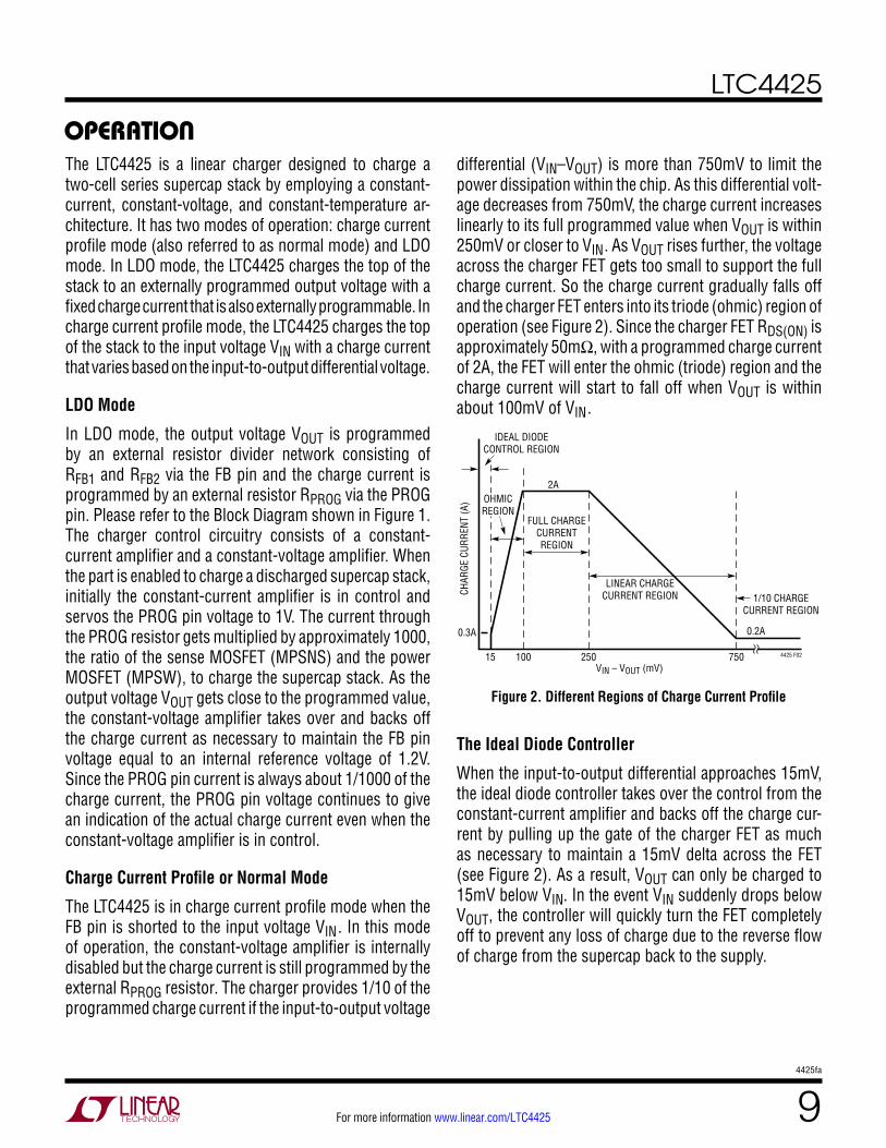
differential (VIN–VOUT) is more than 750mV to limit the power dissipation within the chip. As this differential volt-age decreases from 750mV, the charge current increases linearly to its full programmed value when VOUT is within 250mV or closer to VIN. As VOUT rises further, the voltage across the charger FET gets too small to support the full charge current. So the charge current gradually falls off and the charger FET enters into its triode (ohmic) region of operation (see Figure 2). Since the charger FET RDS(ON) is approximately 50mΩ, with a programmed charge current of 2A, the FET will enter the ohmic (triode) region and the charge current will start to fall off when VOUT is within about 100mV of VIN.
Figure 2. Different Regions of Charge Current Profile
IDEAL DIODECONTROL REGION
OHMICREGION
FULL CHARGECURRENTREGION
LINEAR CHARGECURRENT REGION 1/10 CHARGE
CURRENT REGION
CHAR
GE C
URRE
NT (A
)
0.3A
2A
0.2A
15 100 250 750VIN – VOUT (mV)
4425 F02
The Ideal Diode Controller
When the input-to-output differential approaches 15mV, the ideal diode controller takes over the control from the constant-current amplifier and backs off the charge cur-rent by pulling up the gate of the charger FET as much as necessary to maintain a 15mV delta across the FET (see Figure 2). As a result, VOUT can only be charged to 15mV below VIN. In the event VIN suddenly drops below VOUT, the controller will quickly turn the FET completely off to prevent any loss of charge due to the reverse flow of charge from the supercap back to the supply.

LTC4425
104425fa
For more information www.linear.com/LTC4425
operaTionThermal Regulation
In either mode, if the die temperature starts to approach 105°C due to internal power dissipation, a thermal regula-tor limits the die temperature to approximately 105°C by reducing the charge current. Even in thermal regulation, the PROG pin continues to give an indication of the charge current. The thermal regulation protects the LTC4425 from excessive temperature and allows the user to push the limits of the power handling capability of a given circuit board without the risk of damaging the LTC4425 or the external components. Another benefit of this feature is that the charge current can be set according to typical, rather than worst-case, ambient temperatures for a given applica-tion with the assurance that the charger will automatically reduce the charge current in worst-case conditions.
Voltage Clamp Circuitry
The LTC4425 is equipped with circuitry to limit the voltage across any supercap of the stack to a maximum allowable voltage VCLAMP. There are two preset voltages, 2.45V or 2.7V, for VCLAMP selectable by the SEL pin. The SEL pin should be set to logic low for lower VCLAMP voltage of 2.45V and to logic high for the higher VCLAMP voltage of 2.7V. If the voltage across the bottom capacitor, i.e., the VMID pin voltage reaches VCLAMP first, an NMOS shunt transistor turns on and starts to bleed charge off of the bottom capacitor to GND. Similarly, if the voltage across the top capacitor, VTOP, reaches the VCLAMP voltage first, a PMOS shunt transistor turns on and starts to bleed charge off of the top capacitor to the bottom one.
When the voltage across any of the supercaps reaches within 50mV of VCLAMP, a transconductance amplifier starts to cut back the charge current linearly. By the time any of the shunt devices are on, the charge current gets reduced to 1/10 of the programmed value and stays at this reduced level as long as the shunt device is on. This is to prevent the shunt devices from getting damaged by excessive heat. The comparators that control the shunt devices have a 50mV hysteresis meaning that when the voltage across either capacitor is reduced by 50mV, the shunt devices turn off and normal charging resumes with full charge current unless limited by any of the other amplifiers controlling the gate of the charger FET. In the
event both capacitors exceed their maximum allowable voltage, VCLAMP, the main charger FET completely shuts off and both shunt devices turn on. Both shunt devices are actually current mirrors guaranteed to shunt more current away than that coming through the charger FET.
Leakage Balancing Circuitry
The LTC4425 is equipped with an internal leakage balancing amplifier, LBA, which servos the midpoint, i.e., VMID pin voltage, to exactly half of the output voltage, VOUT. However it has a very limited source and sink capability of approxi-mately 1mA. It is designed to handle slight mismatch of the supercaps due to leakage currents; not to correct any gross mismatch due to defects. The balancer is only active as long as there is an input present. The internal balancer eliminates the need for external balancing resistors.
Short-Circuit Current Limit
In the event the PROG pin gets shorted to GND, the LTC4425 limits the PROG pin current to approximately 3mA which, in turn, limits the maximum charge current to about 3A. While in short-circuit, if one of the supercaps approaches within 50mV of its maximum allowable voltage, VCLAMP, a current-limit foldback circuit cuts back the short-circuit current limit to approximately 1/10 of its full value or to about 300mA.
Supply Status Monitor
The LTC4425 includes an input power-fail comparator, PFC, which monitors the input voltage VIN via the PFI pin. At anytime, if VIN falls below a certain externally programmable threshold, it reports the undervoltage situation by pulling down the open-drain output PFO low. This under-voltage threshold is programmed by connecting an external resis-tor divider network (consisting of RPF1 and RPF2) between VIN and the PFI_RET pins. When the part is enabled, a low RDS(ON) (approx. 13Ω) internal pull-down transistor pulls the bottom end of RPF2, i.e., the PFI_RET pin to GND to complete the divider network. When the part is disabled, this transistor opens RPF2 from GND, thereby saving the current drawn by the divider network. The power-fail com-parator has a built-in filter to reject any transient supply glitch that is less than 10μS long.

LTC4425
114425fa
For more information www.linear.com/LTC4425
operaTionOutput Status Monitor
The LTC4425 has an internal comparator to always monitor the output voltage VOUT. At any time, if VOUT falls below 7.5% of its final programmed value in LDO mode or more than 250mV below the input voltage VIN in charge cur-rent profile mode, the comparator reports the power-fail condition by pulling the same open-drain output PFO low. When both input and output voltages are good for at least 200ms, the PFO pin goes high impedance and can be pulled up to any external supply by a resistor to indicate a power good situation. In normal mode, the load should not exceed 1/10th of the programmed charge current until PFO is high.
VOUT > VIN Operation
If the EN pin is pulled high and VIN is below VOUT or floating, most of the circuitry including the voltage clamp circuitry is kept alive and the part draws about 20µA from the out-put capacitors. However, the internal leakage balancer is turned off under this condition.
Shutdown Mode
The LTC4425 can be shut down by pulling the EN pin low. In shutdown mode, very minimal circuitry is alive and the part draws less than 3µA from the supply or from the output capacitors if the supply is not present.
Charge Current Soft-Start
The LTC4425 includes a soft-start circuit to minimize the inrush current at the start of a charge cycle. When a charge cycle is initiated, the charge current ramps from zero to full-scale over a period of approximately 1ms and this soft-start can be monitored by observing the PROG pin voltage. This has the effect of minimizing the transient current load on the power supply during start-up.
Thermal Shutdown
The LTC4425 includes a thermal shutdown circuit in ad-dition to the thermal regulator. If for any reason, the die temperature exceeds 160°C, the entire part shuts down. It resumes normal operation once the temperature drops by about 14°C, to approximately 146°C.

LTC4425
124425fa
For more information www.linear.com/LTC4425
Programming the Output Voltage
In LDO mode, the LTC4425 output voltage can be pro-grammed for any voltage between 2.7V and VIN by using a resistor divider from VOUT pin to GND via the FB pin such that:
VOUT = VFB • (1 + RFB1/RFB2)
where VFB is 1.2V. See Figure 3.
Typical values for RFB are in the range of 40k to 1M. Too small a resistor will result in a large quiescent current whereas too large a resistor coupled with FB pin capacitance will create an additional pole and may cause loop instability.
applicaTions inForMaTionProgramming the Charge Current
The LTC4425 charge current is programmed using a single resistor from the PROG pin to ground. The charge current out of the VOUT pin is 1000 times the current out of the PROG pin. The program resistor and the charge current are calculated using the following equations:
RPROG = 1000 • (1V/ICHRG), ICHRG = 1000 • (1V/RPROG)
where ICHRG is the charge current out of the VOUT pin. The charge current out of the VOUT pin can be determined at any time by monitoring the PROG pin voltage and using the following equation:
ICHRG = 1000 • (VPROG/RPROG)
Stability Considerations
In LDO mode, the LTC4425 supercapacitor charger has two principal control loops: constant-voltage and constant-current. The constant-voltage loop is stable when connected to a supercap of at least 0.2F. However, when disconnected from the supercap, the voltage loop requires at least 10µF capacitance in series with 500Ω resistance for stability.
In constant-current mode, the PROG pin voltage is in the feedback loop, not the VOUT pin voltage. Because of the additional pole created by the PROG pin capacitance, capacitance on this pin must be kept to a minimum. With no additional capacitance on the PROG pin, the charger is stable with a program resistor as high as 100k. How-ever, any additional capacitance on this node reduces the maximum allowed program resistor. The pole frequency at the PROG pin should be kept above 100kHz. Therefore, if the PROG pin is loaded with a capacitance, CPROG, the following equation should be used to calculate the maxi-mum resistance value for RPROG:
RPROG ≤ 1/(2π • 100kHz • CPROG)
4425 F03
LTC4425
PFI FB
PFI_RET
RPF1
RPF2
RFB1
RFB2
VIN VIN VOUTVOUT
Figure 3. Programming Output Voltage and Input Threshold for Power Fail Comparator.
Programming the Input Voltage Threshold for Power Fail Status Indicator
The input voltage below which the power fail status pin PFO indicates a power-fail condition is programmed by using a resistor divider from the VIN pin to the PFI_RET pin via the PFI pin such that:
VIN, PFO = VPFI • (1 + RPF1/RPF2)
where VPFI is 1.2V. See Figure 3.
Typical values for RPF are in the range of 40k to 1M. In shutdown mode, this divider network is disconnected from ground via the PFI_RET pin to save the quiescent current drawn by the network.

LTC4425
134425fa
For more information www.linear.com/LTC4425
Board Layout Considerations
To be able to deliver maximum charge current under all conditions, it is critical that the exposed metal pad on the backside of the LTC4425’s two packages have a good thermal contact to the PC board ground. Correctly soldered to a 2500mm2 double-sided 1 oz. copper board, the DFN package has a thermal resistance of approximately 43°C/W. Failure to make thermal contact between the exposed pad on the backside of the package and the copper board will result in a thermal resistance far greater than 43°C/W.
Charge Current Reduction by the Thermal Regulator
To protect the part against excessive heat generated by internal power dissipation, the LTC4425 is equipped with a thermal regulator which automatically reduces the charge current to maintain a maximum die temperature of 105°C. Ignoring the quiescent current, the power dissipation can be approximated by the following equation:
PD = (VIN – VOUT) • ICHRG
If θJA is the thermal resistance and TA is the ambient tem-perature, then the die temperature can be calculated as:
TDIE = TA + PD • θJA
When the part is in thermal regulation, the die temperature is 105°C and for a given VIN and VOUT, the charge current can be determined by the following equation:
ICHRG =
105– TAVIN – VOUT( ) • θJA
For example, if the LTC4425 in the DFN package is used in LDO mode to charge a completely discharged supercap stack (VOUT = 0V) at a room temperature of 25°C from a
applicaTions inForMaTion5V source, the charge current, at first, will be limited to approximately:
ICHRG =
105°C– 25°C5– 0( ) V • 43°C / W
=80°C
215°C / A=372mA
As the output voltage rises, the charge current will gradually rise to the full charge current programmed by the PROG pin resistor as long as the constant-current loop is in control. If the LTC4425 is programmed for a charge current of 2A, the output voltage at which the part will deliver full charge current can be determined by the following equation:
VOUT = VIN –
105– TAICHRG • θJA
Using the previous example, for full charge current, the output voltage has to rise to at least:
VOUT =5V –
105– 25( )°C2A • 43°C / W
=5V –80°C
86°C / V= 4.07V
Figure 4 shows the graph of charge current vs output voltage when the charge current profile is turned off by shorting the FB pin to GND and the charge current is limited by thermal regulation.
OUTPUT VOLTAGE (V)0
0
CHAR
GE C
URRE
NT(A
)
2.0
1.5
1.0
0.5
2.5
1 5 62 3 4
4425 F04
VIN = 5VRPROG = 500ΩTA = 25°CFB PIN GROUNDED
THERMAL REGULATION
4.07V
≈ 105°C
372mA
Figure 4. Charge Current vs Output Voltage under Thermal Regulation (LDO Mode)

LTC4425
144425fa
For more information www.linear.com/LTC4425
Figure 5. Charging a Single Supercapacitor
Charging a Single Supercapacitor
The LTC4425 can also be used to charge a single super-capacitor by connecting two series-connected matched ceramic capacitors (minimum 100µF), or two matched series resistors (~470k), in parallel with the supercapacitor as shown in Figure 5. Refer to Table 1 for supercapacitor manufacturers.
Table 1. Supercapacitor ManufacturersCAP-XX www.cap-xx.com
NESS CAP www.nesscap.com
Maxwell www.maxwell.com
Bussmann www.cooperbussmann.com
AVX www.avx.com
Illinois Capacitor www.illcap.com
Tecate Group www.tecategroup.com
applicaTions inForMaTion
C1 = C2 ≥ 100µF
R1
CSUP
VOUT
R1 = R2 = 470k, 1%
R2
4425 F05
LTC4425
VOUT
VMID
GND
C1
CSUP
VOUT
C2
LTC4425
VOUT
VMID
GND

LTC4425
154425fa
For more information www.linear.com/LTC4425
USB to High Peak Power 3.3V Charging
3 × AA Alkaline to High Peak Power 3.3V Charging
VOUT
VMID
FB
PROGPFO
3.3VTOLOAD
2.1M2.2µF
1.2M
2k
470k
1F
1F
VIO
LTC4425
EN
SEL
PFI_RET
PFI
VIN5V, 500mA
USB
1.5M
1.2M
4425 TA03
µC
VOUT
VMID
FB
PROG
PFO
3.3V, 2ATOLOAD
CURRENTMONITOR
2.1M
1.2M
500Ω
470k
1F
1FLTC4425
EN
SEL
PFI_RET
PFI
VIN4.5V TO 3.6V
1.5M
1.2M
3× AA
4425 TA04
µC
VIO
2.2µF
Li-Ion High Peak Power Battery Buffer
VOUT
VMID
PROG
PFO
TOLOAD
CURRENTMONITOR
0.6F
0.6FLTC4425
FBPFI
PFI-RET
EN
Li-Ion
1.5M
500Ω1.2M
470k
SEL
VIN
4425 TA04a
+
VIO
2.2µF
Typical applicaTions
LTC4425
164425fa
For more information www.linear.com/LTC4425
Typical applicaTions
USB
C110µF0805
R1100k
µC
VBUS
D0
D1
D2
NTC
CHRG
CLPROG PROG GND
BAT
GATE
LDO3V3
VOUT
C/X
SW
LTC4088
L13.3µH
M1
+LI-Ion
R42k
R32.94k
C20.1µF0603
R58.2Ω
R2100k
L1: COILCRAFT LPS4018-332MLCM1: SILICONIX Si2333R2: VISHAY-DALE NTHS0603N011-N1003FC1, C3: MURATA GRM21BR61A106KE19C2: MURATA GRM188R71C104KA01CSC: CAP-XX HS203F
INSTANT-ON
CSC0.55FHS203F
VOUTVIN
PFI
SEL
EN
PFO
PFI_RET
VMID
VIN
FB
PROG
GND
R62k
µC
R81.2M
R71.5M
LTC4425
4425 TA05
C310µF0805
5VVIN
LOAD
High Current USB Charging with Power Path Control
3.3V Peak-Power/Back-up Supply
CSC0.55FHS203F
VOUTVIN
PFI
SEL
EN
PFO
PFI_RET
VMID
VIN
FB
PROG
GND2k
µC
1.2M
1.5MLTC4425
4425 TA05a
SW1
PVIN
VIN
RUN/SS
RT
SW2
PVOUT
VOUT
FB
LTC3533
10µF
5VVIN
≈5V
340k 6.49k
100µF
47pF
VOUT3.3V1.5A
200k0.1µF
107k330pF
4.7pF
2.2µH
33.2k 200kPGNDSGND
ONOFF
BURST
VC
2.2µF
LTC4425
174425fa
For more information www.linear.com/LTC4425
Typical applicaTions
LTC4425
VIN
FB
PFI
SEL
EN
PFO
PFI_RET
VOUT
VMID
PROG
GND
CSP11F
CSP21F
µC
R81.2M
1.5M
11k
R62k
VOUT
SW
ISENSE
FB
ILIM
VIN
59k
28.7k
GND
2.2µF
LT3663
RUN
BOOST
OFFON
0.1µF
D1
22µF
5V INSTANT-ON
6.8µH D1: DFLS240CSP1, CSP2:
12V
4425 TA07
5V HIGH-PEAK POWER,OR BACKUP SUPPLY
12V Input to 5V Outputs with Input Voltage Monitoring
CSP11F
CSP21F
3.3V
5V
VOUTVIN
VOUT (5V)VIN
SHDN
RT GND VC
FB
SW
BOOST
PFI
SEL
EN
PFO
PFI_RET
VMID
FB
PROG
GND
R62k 1.2M
2.1M
µC
R81.2M
R71.5M
LTC4425LT3505
4425 TA06
12V
10µF
68pF
11.3k
61.1k
10µH0.1µF
D1
D2
69.8k75k
70pF1µF
D1: 1N4148D2: MBRM140CSP1, CSP2: CAP-XX HS203F
HIGH PEAK-POWER LOAD
12V to 5V/3.3V High Peak Power Supply

LTC4425
184425fa
For more information www.linear.com/LTC4425
Redundant High Peak Power Battery Supplies
LTC4425
LTC4425
SEL
EN
PFO
PFO
FB
PFI
PFI_RET
VIN
SEL
EN
FBPFI
PFI_RET
VIN
VOUT
VMID
VOUT
VIO
VMID
1.2M
1.5M2.2µF
PROG
PROG
2k
500Ω
470k
1.5M3×AA
1.2M
4425 TA08
USB
TO LOAD
BAT POWER OK
USB POWER OK
1F
1F
µC
2.2µF
Typical applicaTions

LTC4425
194425fa
For more information www.linear.com/LTC4425
package DescripTionPlease refer to http://www.linear.com/product/LTC4425#packaging for the most recent package drawings.
3.00 ±0.10(4 SIDES)
NOTE:1. DRAWING IS NOT A JEDEC PACKAGE OUTLINE2. DRAWING NOT TO SCALE3. ALL DIMENSIONS ARE IN MILLIMETERS4. DIMENSIONS OF EXPOSED PAD ON BOTTOM OF PACKAGE DO NOT INCLUDE MOLD FLASH. MOLD FLASH, IF PRESENT, SHALL NOT EXCEED 0.15mm ON ANY SIDE5. EXPOSED PAD AND TIE BARS SHALL BE SOLDER PLATED6. SHADED AREA IS ONLY A REFERENCE FOR PIN 1 LOCATION ON THE TOP AND BOTTOM OF PACKAGE
0.40 ±0.10
BOTTOM VIEW—EXPOSED PAD
1.65 ±0.10
0.75 ±0.05
R = 0.115TYP
16
127
PIN 1TOP MARK
(SEE NOTE 6)
0.200 REF
0.00 – 0.05
(DD12) DFN 0106 REV A
RECOMMENDED SOLDER PAD PITCH AND DIMENSIONSAPPLY SOLDER MASK TO AREAS THAT ARE NOT SOLDERED
0.23 ±0.05
0.25 ±0.05
2.25 REF
2.38 ±0.051.65 ±0.052.10 ±0.05
0.70 ±0.05
3.50 ±0.05
PACKAGEOUTLINE
PIN 1 NOTCHR = 0.20 OR0.25 × 45°CHAMFER
2.38 ±0.10
2.25 REF0.45 BSC
0.45 BSC
DD Package12-Lead Plastic DFN (3mm × 3mm)
(Reference LTC DWG # 05-08-1725 Rev A)

LTC4425
204425fa
For more information www.linear.com/LTC4425
package DescripTionPlease refer to http://www.linear.com/product/LTC4425#packaging for the most recent package drawings.
MSOP (MSE12) 0213 REV G
0.53 ±0.152(.021 ±.006)
SEATINGPLANE
0.18(.007)
1.10(.043)MAX
0.22 – 0.38(.009 – .015)
TYP
0.86(.034)REF
0.650(.0256)
BSC
12
12 11 10 9 8 7
7
DETAIL “B”
1 6
NOTE:1. DIMENSIONS IN MILLIMETER/(INCH)2. DRAWING NOT TO SCALE3. DIMENSION DOES NOT INCLUDE MOLD FLASH, PROTRUSIONS OR GATE BURRS. MOLD FLASH, PROTRUSIONS OR GATE BURRS SHALL NOT EXCEED 0.152mm (.006") PER SIDE4. DIMENSION DOES NOT INCLUDE INTERLEAD FLASH OR PROTRUSIONS. INTERLEAD FLASH OR PROTRUSIONS SHALL NOT EXCEED 0.152mm (.006") PER SIDE5. LEAD COPLANARITY (BOTTOM OF LEADS AFTER FORMING) SHALL BE 0.102mm (.004") MAX6. EXPOSED PAD DIMENSION DOES INCLUDE MOLD FLASH. MOLD FLASH ON E-PAD SHALL NOT EXCEED 0.254mm (.010") PER SIDE.
0.254(.010) 0° – 6° TYP
DETAIL “A”
DETAIL “A”
GAUGE PLANE
RECOMMENDED SOLDER PAD LAYOUT
BOTTOM VIEW OFEXPOSED PAD OPTION
2.845 ±0.102(.112 ±.004)2.845 ±0.102
(.112 ±.004)
4.039 ±0.102(.159 ±.004)
(NOTE 3)
1.651 ±0.102(.065 ±.004)
1.651 ±0.102(.065 ±.004)
0.1016 ±0.0508(.004 ±.002)
1 2 3 4 5 6
3.00 ±0.102(.118 ±.004)
(NOTE 4)
0.406 ±0.076(.016 ±.003)
REF
4.90 ±0.152(.193 ±.006)
DETAIL “B”CORNER TAIL IS PART OF
THE LEADFRAME FEATURE.FOR REFERENCE ONLY
NO MEASUREMENT PURPOSE
0.12 REF
0.35REF
5.10(.201)MIN
3.20 – 3.45(.126 – .136)
0.889 ±0.127(.035 ±.005)
0.42 ±0.038(.0165 ±.0015)
TYP
0.65(.0256)
BSC
MSE Package12-Lead Plastic MSOP, Exposed Die Pad
(Reference LTC DWG # 05-08-1666 Rev G)

LTC4425
214425fa
For more information www.linear.com/LTC4425
Information furnished by Linear Technology Corporation is believed to be accurate and reliable. However, no responsibility is assumed for its use. Linear Technology Corporation makes no representa-tion that the interconnection of its circuits as described herein will not infringe on existing patent rights.
revision hisToryREV DATE DESCRIPTION PAGE NUMBER
A 02/16 Enhanced Charging a Single Supercapacitor section 14

LTC4425
224425fa
For more information www.linear.com/LTC4425
Linear Technology Corporation1630 McCarthy Blvd., Milpitas, CA 95035-7417
LINEAR TECHNOLOGY CORPORATION 2010
LT 0216 REV A • PRINTED IN USA
(408) 432-1900 ● FAX: (408) 434-0507 ● www.linear.com/LTC4425
relaTeD parTsPART NUMBER DESCRIPTION COMMENTS
LTC3225-1 LTC3225
150mA Supercapacitor Charger Programmable Supercapacitor Charger Designed to Charge Two Supercapacitors in Series to a Fixed Output Voltage (4.8V/5/3V Selectable)
LT3485-0/LT3485-1/ LT3485-2/LT3485-3
1.4A/0.7A/1A/2A Photoflash Capacitor Charger with Output Voltage Monitor and IGBT
VIN; 1.8V to 10V, Charge Time = 3.7 Seconds for the LT3485-0 (0V to 320V, 100µF, VIN = 3.6V), ISD < 1µA, 3mm × 3mm 10-Lead DFN
LT3750 Capacitor Charger Controller Charges Any Size Capacitor, 10-Lead MS Package
LT3751 Capacitor Controller with Regulation Charges Any Size Capacitor, 4mm × 5mm QFN-20 Package
LTC4040 Buck Battery Charger + Boost Backup for Li-Ion Batteries 2.5A Backup from 3.2V Battery 4mm × 5mm QFN-24 Package
LTC3643 Bi-Directional Boost Charger/Buck Backup for Electrolytic Caps
VIN; 3V to 17V, VBACKUP: Up to 40V, 2A Cap Charge Current, 3mm × 5mm QFN-24
Typical applicaTion
LTC4425
LTC3569(UD PACKAGE)
VIN
FB
PFI
SEL
EN
PFO
PFI_RET
VOUTVOUT (5V)
VMID
PROG
GND
CSP11F
CSP21F
8
4
6µC
11, 12
R71.5M
R81.2M
9
5
7 3
13
10
1, 2 5V, 2A
R6500Ω
SVIN PVIN, 1, 2, 3SW1
PGND, 1, 2, 3
SGND
SW2
SW3
PGOOD
FB1
FB2
FB3
L22.2µH
10µF20pF 750k
240k
SW
BIAS
FB
VC
PG
RT
VIN BD
10µF200k
28.7k
L12.2µH
22µF
590k
20k
GND
2.2µF
LT3684
RUN BOOST
3.3V
L32.5µH
4.7µF20pF 300k
240k
1.8V
L42.5µH
4.7µF20pF 150k
240k
1.2V
OFFONCAR
BATTERY
D1
330pF
6V to 36V
0.1µF
EN1
EN2
EN3
MODE
RT
D1: DIODES INC. DFLS240L1: SUMIDA CDRH4D22/HP-2R2L2: WURTH 7440430022L3, L4 WURTH 744031002CSP1, CSP2: CAP-XX HS203F
4425 TA09
Embedded Automotive Backup Controller