Embed Size (px)
Citation preview
LTC5585
15585fb
For more information www.linear.com/LTC5585
TYPICAL APPLICATION
FEATURES DESCRIPTION
Wideband IQ Demodulator with IIP2 and DC Offset
Control
The LTC®5585 is a direct conversion quadrature demodu-lator optimized for high linearity receiver applications in the 400MHz to 4GHz frequency range. It is suitable for communications receivers where an RF signal is directly converted into I and Q baseband signals with bandwidth of 530MHz or higher. The LTC5585 incorporates balanced I and Q mixers, LO buffer amplifiers and a precision, high frequency quadrature phase shifter. The integrated on-chip broadband transformer provides a single-ended interface at the RF input with simple off-chip L-C matching. In ad-dition, the LTC5585 provides four analog control voltage interface pins for IIP2 and DC offset correction, greatly simplifying system calibration.
The high linearity of the LTC5585 provides excellent spur-free dynamic range for the receiver. This direct conversion demodulator can eliminate the need for intermediate fre-quency (IF) signal processing, as well as the corresponding requirements for image filtering and IF filtering. These I/Q outputs can interface directly to channel-select filters (LPFs) or to baseband amplifiers.L, LT, LTC, LTM, Linear Technology and the Linear logo are registered trademarks of Linear Technology Corporation. All other trademarks are the property of their respective owners.
Direct Conversion Receiver with IIP2 and DC Offset Calibration
APPLICATIONS
n 400MHz to 4GHz Operating Frequencyn High IIP3: 28.7dBm at 700MHz, 25.7dBm at 1.95GHzn High IIP2: 70dBm at 700MHz, 60dBm at 1.95GHzn User Adjustable IIP2 Up to 80dBmn User Adjustable DC Offset Nulln High Input P1dB: 16dBm at 1950MHzn I/Q Bandwidth of 530MHz or Highern Image Rejection: 43dB at 1950MHzn Noise Figure: 13.5dB at 700MHz 12.7dB at 1.95GHzn Conversion Gain: 2.0dB at 700MHz 2.4dB at 1.95GHzn Single-Ended RF with On-Chip Transformern Shutdown Moden Operating Temperature Range (TC): –40°C to 105°Cn 24-Lead 4mm × 4mm QFN Package
n LTE/W-CDMA/TD-SCDMA Base Station Receiversn Wideband DPD Receiversn Point-To-Point Broadband Radiosn High Linearity Direct Conversion I/Q Receiversn Image Rejection Receivers
A/D
D/A
D/A
VGA
VGA
5585 TA01a
LPFRF
BPFLNABPF RFINPUT
LO
EN
LO INPUT
ENABLE
LPF
IP2 ADJUST
DC OFFSET
I+
I–
Q+
Q–
0°
90°
IP2 AND DCOFFSET CAL
LTC5585
VCC
5V
IP2 ADJUST
DC OFFSETIP2 AND DCOFFSET CAL
D/A
D/A
A/D
IIP2 vs IP2I, IP2Q Trim Voltage
IP2I, IP2Q (V)0
IIP2
(dBm
)
80
90
100
0.8 0.9
5585 G09
70
60
400.2 0.4 0.60.1 1.00.3 0.5 0.7
50
120fRF = 700MHz
110
I, –40°CI, 25°CI, 85°CI, 105°C
Q, –40°CQ, 25°CQ, 85°CQ, 105°C
LTC5585
25585fb
For more information www.linear.com/LTC5585
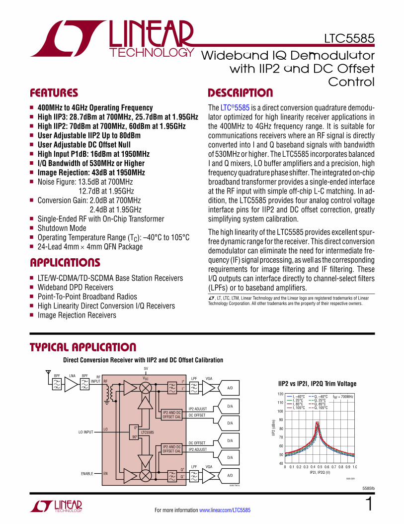
PIN CONFIGURATIONABSOLUTE MAXIMUM RATINGS
VCC Supply Voltage ................................... –0.3V to 5.5VVCAP Voltage .................................................VCC ±0.05V I–, I+, Q+, Q–, CMI, CMQ Voltage ........2.5V to VCC + 0.3VVoltage on Any Other Pin .................–0.3V to VCC + 0.3VLO+, LO–, RF Input Power ....................................20dBmRF Input DC Voltage ............................................... ±0.1VMaximum Junction Temperature (TJMAX) ............. 150°COperating Temperature Range (TC) ........ –40°C to 105°CStorage Temperature Range .................. –65°C to 150°C
(Note 1)
24 23 22 21 20 19
7 8 9
TOP VIEW
25GND
UF PACKAGE24-LEAD (4mm × 4mm) PLASTIC QFN
10 11 12
6
5
4
3
2
1
13
14
15
16
17
18IP2Q
DCOQ
DCOI
IP2I
RF
GND
CMQ
VCAP
LO–
LO+
GND
GND
REF
I+ I– Q+ Q– CMI
EN
GND
V BIA
S
V CC
EDC
EIP2
TJMAX = 150°C, θJC = 7°C/W
EXPOSED PAD (PIN 25) IS GND, MUST BE SOLDERED TO PCB
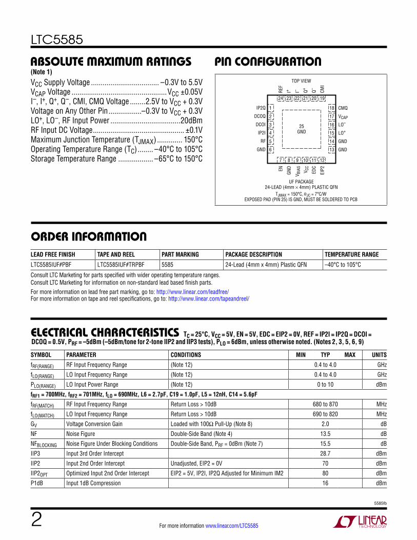
ELECTRICAL CHARACTERISTICS TC = 25°C, VCC = 5V, EN = 5V, EDC = EIP2 = 0V, REF = IP2I = IP2Q = DCOI = DCOQ = 0.5V, PRF = –5dBm (–5dBm/tone for 2-tone IIP2 and IIP3 tests), PLO = 6dBm, unless otherwise noted. (Notes 2, 3, 5, 6, 9)
ORDER INFORMATIONLEAD FREE FINISH TAPE AND REEL PART MARKING PACKAGE DESCRIPTION TEMPERATURE RANGE
LTC5585IUF#PBF LTC5585IUF#TRPBF 5585 24-Lead (4mm x 4mm) Plastic QFN –40°C to 105°C
Consult LTC Marketing for parts specified with wider operating temperature ranges. Consult LTC Marketing for information on non-standard lead based finish parts.For more information on lead free part marking, go to: http://www.linear.com/leadfree/ For more information on tape and reel specifications, go to: http://www.linear.com/tapeandreel/
SYMBOL PARAMETER CONDITIONS MIN TYP MAX UNITS
fRF(RANGE) RF Input Frequency Range (Note 12) 0.4 to 4.0 GHz
fLO(RANGE) LO Input Frequency Range (Note 12) 0.4 to 4.0 GHz
PLO(RANGE) LO Input Power Range (Note 12) 0 to 10 dBm
fRF1 = 700MHz, fRF2 = 701MHz, fLO = 690MHz, L6 = 2.7pF, C19 = 1.0pF, L5 = 12nH, C14 = 5.6pF
fRF(MATCH) RF Input Frequency Range Return Loss > 10dB 680 to 870 MHz
fLO(MATCH) LO Input Frequency Range Return Loss > 10dB 690 to 820 MHz
GV Voltage Conversion Gain Loaded with 100Ω Pull-Up (Note 8) 2.0 dB
NF Noise Figure Double-Side Band (Note 4) 13.5 dB
NFBLOCKING Noise Figure Under Blocking Conditions Double-Side Band, PRF = 0dBm (Note 7) 15.5 dB
IIP3 Input 3rd Order Intercept 28.7 dBm
IIP2 Input 2nd Order Intercept Unadjusted, EIP2 = 0V 70 dBm
IIP2OPT Optimized Input 2nd Order Intercept EIP2 = 5V, IP2I, IP2Q Adjusted for Minimum IM2 80 dBm
P1dB Input 1dB Compression 16 dBm
LTC5585
35585fb
For more information www.linear.com/LTC5585
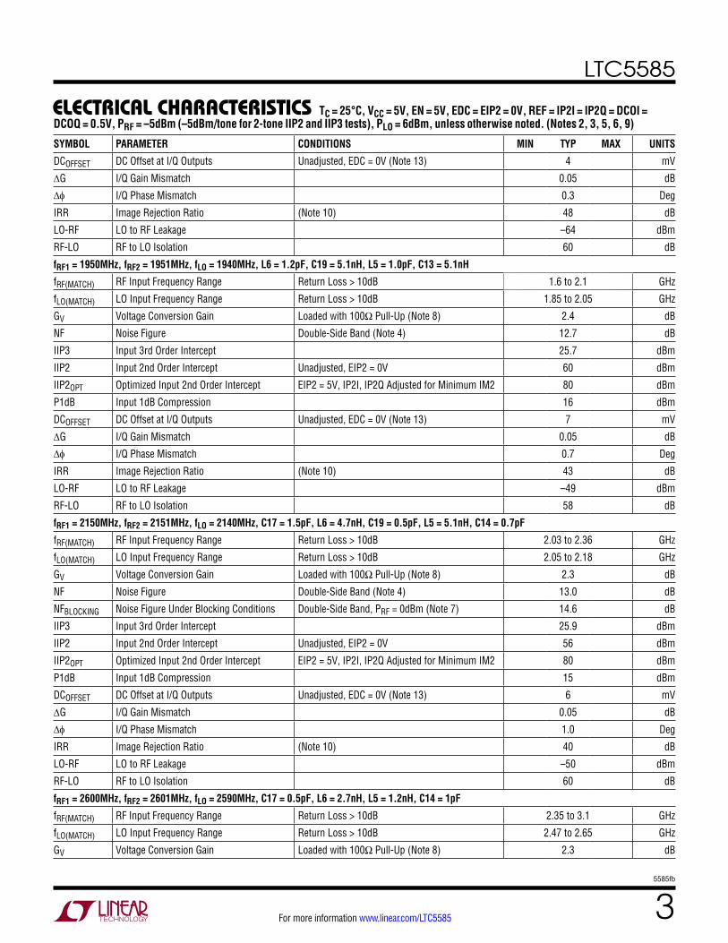
ELECTRICAL CHARACTERISTICS TC = 25°C, VCC = 5V, EN = 5V, EDC = EIP2 = 0V, REF = IP2I = IP2Q = DCOI = DCOQ = 0.5V, PRF = –5dBm (–5dBm/tone for 2-tone IIP2 and IIP3 tests), PLO = 6dBm, unless otherwise noted. (Notes 2, 3, 5, 6, 9)
SYMBOL PARAMETER CONDITIONS MIN TYP MAX UNITS
DCOFFSET DC Offset at I/Q Outputs Unadjusted, EDC = 0V (Note 13) 4 mV
∆G I/Q Gain Mismatch 0.05 dB
∆φ I/Q Phase Mismatch 0.3 Deg
IRR Image Rejection Ratio (Note 10) 48 dB
LO-RF LO to RF Leakage –64 dBm
RF-LO RF to LO Isolation 60 dB
fRF1 = 1950MHz, fRF2 = 1951MHz, fLO = 1940MHz, L6 = 1.2pF, C19 = 5.1nH, L5 = 1.0pF, C13 = 5.1nH
fRF(MATCH) RF Input Frequency Range Return Loss > 10dB 1.6 to 2.1 GHz
fLO(MATCH) LO Input Frequency Range Return Loss > 10dB 1.85 to 2.05 GHz
GV Voltage Conversion Gain Loaded with 100Ω Pull-Up (Note 8) 2.4 dB
NF Noise Figure Double-Side Band (Note 4) 12.7 dB
IIP3 Input 3rd Order Intercept 25.7 dBm
IIP2 Input 2nd Order Intercept Unadjusted, EIP2 = 0V 60 dBm
IIP2OPT Optimized Input 2nd Order Intercept EIP2 = 5V, IP2I, IP2Q Adjusted for Minimum IM2 80 dBm
P1dB Input 1dB Compression 16 dBm
DCOFFSET DC Offset at I/Q Outputs Unadjusted, EDC = 0V (Note 13) 7 mV
∆G I/Q Gain Mismatch 0.05 dB
∆φ I/Q Phase Mismatch 0.7 Deg
IRR Image Rejection Ratio (Note 10) 43 dB
LO-RF LO to RF Leakage –49 dBm
RF-LO RF to LO Isolation 58 dB
fRF1 = 2150MHz, fRF2 = 2151MHz, fLO = 2140MHz, C17 = 1.5pF, L6 = 4.7nH, C19 = 0.5pF, L5 = 5.1nH, C14 = 0.7pF
fRF(MATCH) RF Input Frequency Range Return Loss > 10dB 2.03 to 2.36 GHz
fLO(MATCH) LO Input Frequency Range Return Loss > 10dB 2.05 to 2.18 GHz
GV Voltage Conversion Gain Loaded with 100Ω Pull-Up (Note 8) 2.3 dB
NF Noise Figure Double-Side Band (Note 4) 13.0 dB
NFBLOCKING Noise Figure Under Blocking Conditions Double-Side Band, PRF = 0dBm (Note 7) 14.6 dB
IIP3 Input 3rd Order Intercept 25.9 dBm
IIP2 Input 2nd Order Intercept Unadjusted, EIP2 = 0V 56 dBm
IIP2OPT Optimized Input 2nd Order Intercept EIP2 = 5V, IP2I, IP2Q Adjusted for Minimum IM2 80 dBm
P1dB Input 1dB Compression 15 dBm
DCOFFSET DC Offset at I/Q Outputs Unadjusted, EDC = 0V (Note 13) 6 mV
∆G I/Q Gain Mismatch 0.05 dB
∆φ I/Q Phase Mismatch 1.0 Deg
IRR Image Rejection Ratio (Note 10) 40 dB
LO-RF LO to RF Leakage –50 dBm
RF-LO RF to LO Isolation 60 dB
fRF1 = 2600MHz, fRF2 = 2601MHz, fLO = 2590MHz, C17 = 0.5pF, L6 = 2.7nH, L5 = 1.2nH, C14 = 1pF
fRF(MATCH) RF Input Frequency Range Return Loss > 10dB 2.35 to 3.1 GHz
fLO(MATCH) LO Input Frequency Range Return Loss > 10dB 2.47 to 2.65 GHz
GV Voltage Conversion Gain Loaded with 100Ω Pull-Up (Note 8) 2.3 dB
LTC5585
45585fb
For more information www.linear.com/LTC5585
ELECTRICAL CHARACTERISTICS TC = 25°C, VCC = 5V, EN = 5V, EDC = EIP2 = 0V, REF = IP2I = IP2Q = DCOI = DCOQ = 0.5V, PRF = –5dBm (–5dBm/tone for 2-tone IIP2 and IIP3 tests), PLO = 6dBm, unless otherwise noted. (Notes 2, 3, 5, 6, 9)
SYMBOL PARAMETER CONDITIONS MIN TYP MAX UNITS
NF Noise Figure Double-Side Band (Note 4) 13.6 dB
NFBLOCKING Noise Figure Under Blocking Conditions Double-Side Band, PRF = 0dBm (Note 7) 15.2 dB
IIP3 Input 3rd Order Intercept 27.5 dBm
IIP2 Input 2nd Order Intercept Unadjusted, EIP2 = 0V 60 dBm
IIP2OPT Minimum Input 2nd Order Intercept EIP2 = 5V, IP2I, IP2Q Adjusted for Minimum IM2 80 dBm
P1dB Input 1dB Compression 15.5 dBm
DCOFFSET DC Offset at I/Q Outputs Unadjusted, EDC = 0V (Note 13) 8 mV
∆G I/Q Gain Mismatch 0.05 dB
∆φ I/Q Phase Mismatch 1.0 Deg
IRR Image Rejection Ratio (Note 10) 40 dB
LO-RF LO to RF Leakage –46 dBm
RF-LO RF to LO Isolation 55 dB
fRF1 = 3500MHz, fRF2 = 3501MHz, fLO = 3490MHz, C17 = 0.6pF, L6 = 1.0nH, C13 = 0.7pF, L5 = Short, C14 = Open, Single-Ended LO (See Figure 14)
fRF(MATCH) RF Input Frequency Range Return Loss > 10dB 2.88 to 3.97 GHz
fLO(MATCH) LO Input Frequency Range Return Loss > 10dB 2.97 to 3.96 GHz
GV Voltage Conversion Gain Loaded with 100Ω Pull-Up (Note 8) 0.3 dB
NF Noise Figure Double-Side Band (Note 4) 17.1 dB
IIP3 Input 3rd Order Intercept 28.1 dBm
IIP2 Input 2nd Order Intercept Unadjusted, EIP2 = 0V 52.5 dBm
IIP2OPT Minimum Input 2nd Order Intercept EIP2 = 5V, IP2I, IP2Q Adjusted for Minimum IM2 65.9 dBm
P1dB Input 1dB Compression 17.1 dBm
DCOFFSET DC Offset at I/Q Outputs Unadjusted, EDC = 0V (Note 13) 16.5 mV
∆G I/Q Gain Mismatch 0.04 dB
∆φ I/Q Phase Mismatch 1.8 Deg
IRR Image Rejection Ratio (Note 10) 36 dB
LO-RF LO to RF Leakage –34.7 dBm
RF-LO RF to LO Isolation 44.5 dB
Power Supply and Other Parameters
VCC Supply Voltage 4.75 5.0 5.25 V
ICC Supply Current EDC = EIP2 = 5V 180 200 220 mA
ICC(LOW) Supply Current EDC = EIP2 = 0V 170 190 210 mA
ICC(OFF) Shutdown Current EN < 0.3V 11 900 μA
tON Turn-On Time EN Transition from Logic Low to High (Note 14) 0.2 µs
tOFF Turn-Off Time EN Transition from Logic High to Low (Note 15) 0.8 µs
VEH EN, EDC, EIP2 Input High Voltage (On) 2.0 V
VEL EN, EDC, EIP2 Input Low Voltage (Off) 0.3 V
IENH EN Pin Input Current EN = 5.0V 52 μA
IEDCH EDC Pin Input Current EDC = 5.0V 33 μA
LTC5585
55585fb
For more information www.linear.com/LTC5585
ELECTRICAL CHARACTERISTICS
Note 1: Stresses beyond those listed under Absolute Maximum Ratings may cause permanent damage to the device. Exposure to any Absolute Maximum Rating condition for extended periods may affect device reliability and lifetime.Note 2: Tests are performed with the test circuit of Figure 1.Note 3: The LTC5585 is guaranteed to be functional over the –40°C to 105°C case temperature operating range.Note 4: DSB noise figure is measured at the baseband frequency of 15MHz with a small-signal noise source without any filtering on the RF input and no other RF signal applied.Note 5: Performance at the RF frequencies listed is measured with external RF and LO impedance matching, as shown in the table of Figure 1.Note 6: The complementary outputs (I+, I– and Q+, Q–) are combined using a 180° phase-shift combiner.Note 7: Noise figure under blocking conditions (NFBLOCKING) is measured at an output frequency of 60MHz with RF input signal at fLO + 1MHz. Both RF and LO input signals are appropriately filtered, as well as the baseband output. NFBLOCKING measured at 840MHz, 2140MHz and 2500MHz only.
Note 8: Voltage conversion gain is calculated from the average measured power conversion gain of the I and Q outputs using the test circuit shown in Figure 1. Power conversion gain is measured with a 100Ω differential load impedance on the I and Q outputs.Note 9: Baseband outputs have a 100Ω external pull-up resistor to VCC as shown in the test circuit shown in Figure 1.Note 10: Image rejection is calculated from the measured gain error and phase error using the method listed in the appendix.Note 11: The DCOI, DCOQ, IP2I, IP2Q pins have an 8k internal resistor to ground. The REF pin has a 2k internal resistor to ground. If unconnected, these pins will float up to 500mV through internal current sources. A low output resistance voltage source is recommended for driving these pins.Note 12: This is the recommended operating range, operation outside the listed range is possible with degraded performance to some parameters.Note 13: DC offset measured differentially between I+ and I– and between Q+ and Q–. The reported value is the mean of the absolute values of the characterization data distribution. Note 14: Baseband amplitude is within 10% of final value.Note 15: Baseband amplitude is at least 30dB down from its on state.
SYMBOL PARAMETER CONDITIONS MIN TYP MAX UNITS
IEIP2H EIP2 Pin Input Current EIP2 = 5.0V 50 μA
VREF REF Pin Voltage With REF Pin Unloaded 0.5 V
VREF(RANGE) REF Pin Voltage Range When Driven with External Source 0.4 to 0.7 V
ZREF REF Input Impedance (Note 11) 2||1 kΩ||pF
DCOI, DCOQ, IP2I, IP2Q Pin Voltage Unloaded 0.5 V
DCOI, DCOQ, IP2I, IP2Q Voltage Range When Driven with External Source 0 to 2VREF V
DCOI, DCOQ, IP2I, IP2Q Impedance (Note 11) 8||1 kΩ||pF
DCOI, DCOQ, IP2I, IP2Q Settling Time For Step Input, Output with 90% of Final Value 20 ns
DC Offset Adjustment Range DCOI, DCOQ Swept from 0V to 1V, EDC = 5V ±20 mV
DC Offset Drift Over Temperature Unadjusted, EDC = 0V 20 μV/°C
VCM I+, I–, Q+, Q– Common Mode Voltage VCC – 1.5 V
ZOUT I+, I–, Q+, Q– Output Impedance Single Ended 100||6 Ω||pF
BWBB I+, I–, Q+, Q– Output Bandwidth 100Ω External Pull-Up, –3dB Corner Frequency 530 MHz
LTC5585
65585fb
For more information www.linear.com/LTC5585
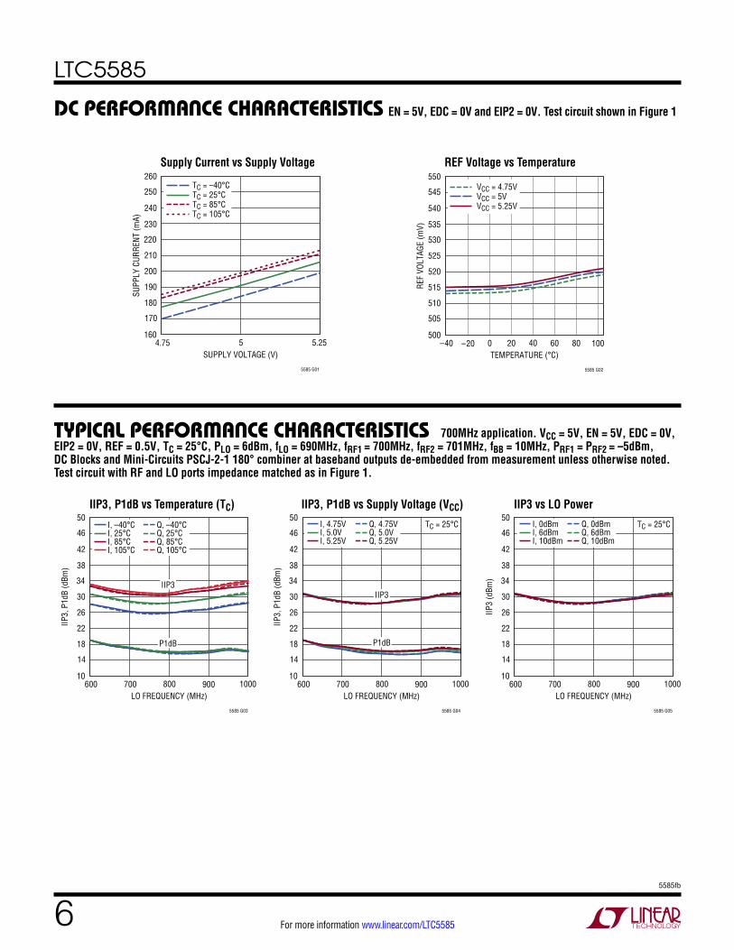
DC PERFORMANCE CHARACTERISTICS
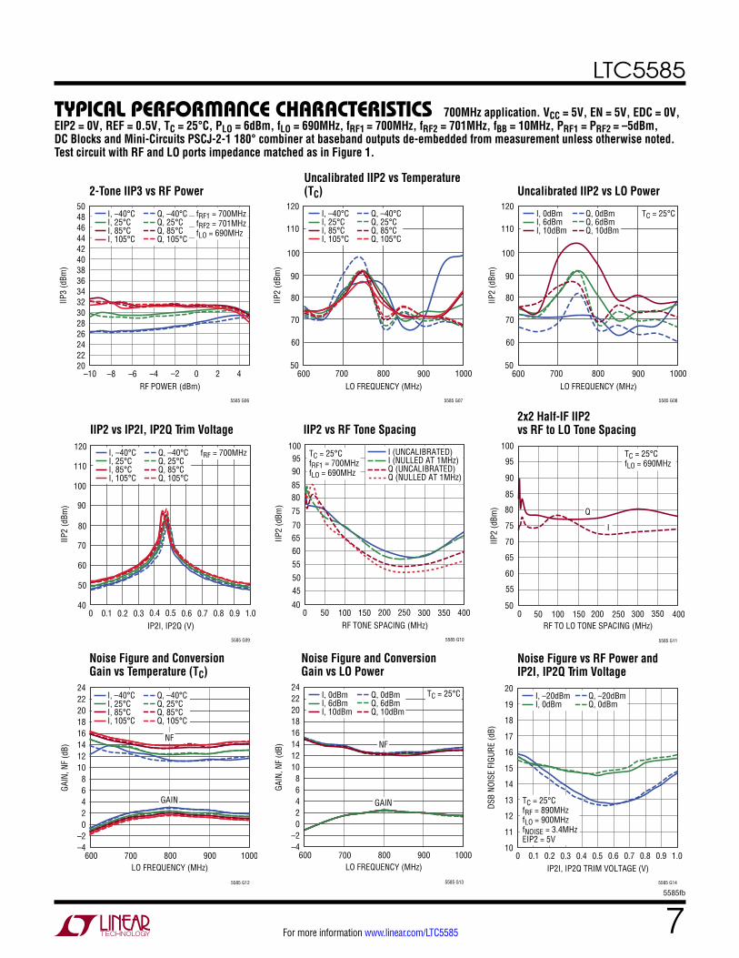
TYPICAL PERFORMANCE CHARACTERISTICS
IIP3, P1dB vs Temperature (TC) IIP3, P1dB vs Supply Voltage (VCC) IIP3 vs LO Power
Supply Current vs Supply Voltage REF Voltage vs Temperature
EN = 5V, EDC = 0V and EIP2 = 0V. Test circuit shown in Figure 1
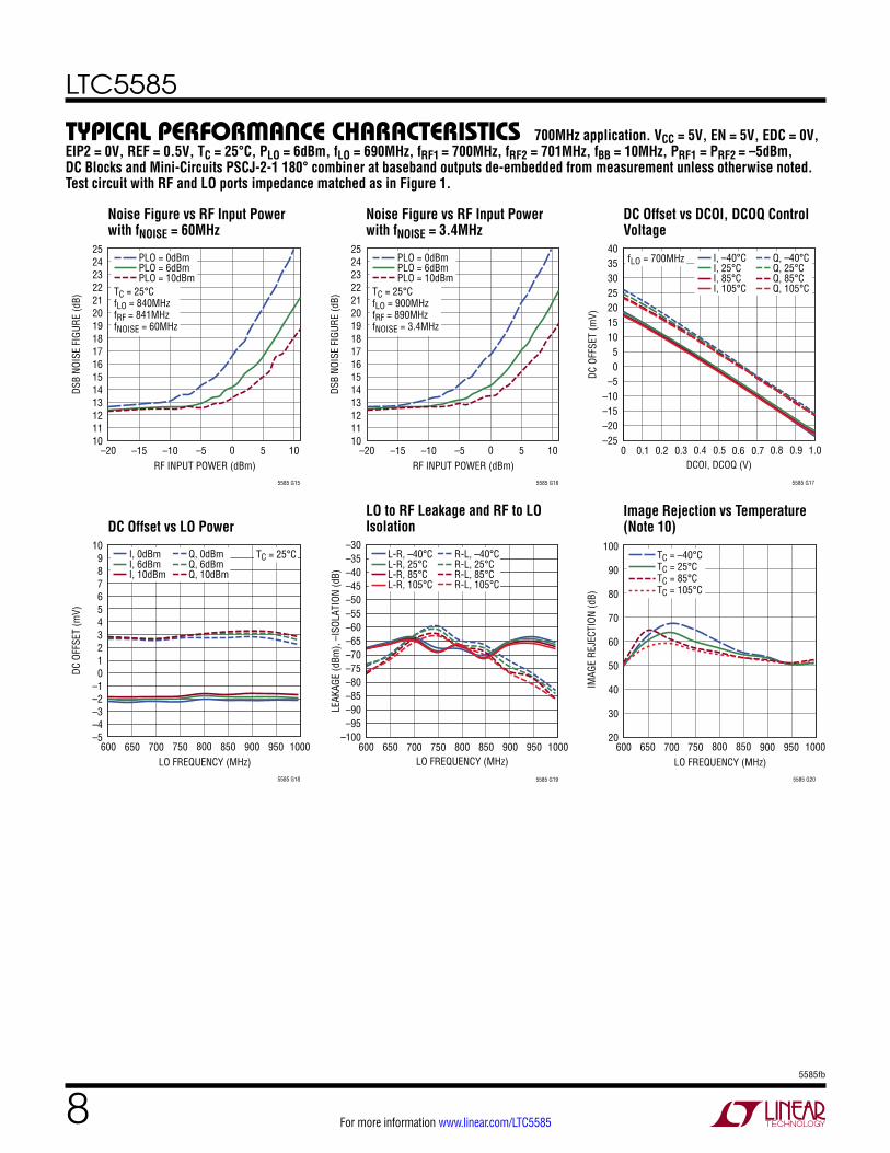
700MHz application. VCC = 5V, EN = 5V, EDC = 0V, EIP2 = 0V, REF = 0.5V, TC = 25°C, PLO = 6dBm, fLO = 690MHz, fRF1 = 700MHz, fRF2 = 701MHz, fBB = 10MHz, PRF1 = PRF2 = –5dBm, DC Blocks and Mini-Circuits PSCJ-2-1 180° combiner at baseband outputs de-embedded from measurement unless otherwise noted. Test circuit with RF and LO ports impedance matched as in Figure 1.
SUPPLY VOLTAGE (V)4.75
160
SUPP
LY C
URRE
NT (m
A)
170
190
200
210
260
230
5
5585 G01
180
240
250
220
5.25
TC = –40°CTC = 25°CTC = 85°CTC = 105°C
TEMPERATURE (°C)–40
500
REF
VOLT
AGE
(mV)
505
515
520
525
550
535
0 40 60 80
5585 G02
510
540
545
530
–20 20 100
VCC = 4.75VVCC = 5VVCC = 5.25V
LO FREQUENCY (MHz)600
10
IIP3,
P1d
B (d
Bm)
14
22
26
30
50
38
700 800
5585 G03
18
42
46
34
900 1000
I, –40°CI, 25°CI, 85°CI, 105°C
Q, –40°CQ, 25°CQ, 85°CQ, 105°C
IIP3
P1dB
LO FREQUENCY (MHz)600
10
IIP3,
P1d
B (d
Bm)
14
22
26
30
50TC = 25°C
38
700 800
5585 G04
18
42
46
34
900 1000
I, 4.75VI, 5.0VI, 5.25V
Q, 4.75VQ, 5.0VQ, 5.25V
IIP3
P1dB
LO FREQUENCY (MHz)600
10
IIP3
(dBm
)
14
22
26
30
50TC = 25°C
38
700 800
5585 G05
18
42
46
34
900 1000
I, 0dBmI, 6dBmI, 10dBm
Q, 0dBmQ, 6dBmQ, 10dBm
LTC5585
75585fb
For more information www.linear.com/LTC5585
TYPICAL PERFORMANCE CHARACTERISTICS
IIP2 vs IP2I, IP2Q Trim Voltage IIP2 vs RF Tone Spacing2x2 Half-IF IIP2 vs RF to LO Tone Spacing
Noise Figure and Conversion Gain vs LO Power
Noise Figure and Conversion Gain vs Temperature (TC)
2-Tone IIP3 vs RF PowerUncalibrated IIP2 vs Temperature (TC)
Noise Figure vs RF Power and IP2I, IP2Q Trim Voltage
Uncalibrated IIP2 vs LO Power
700MHz application. VCC = 5V, EN = 5V, EDC = 0V, EIP2 = 0V, REF = 0.5V, TC = 25°C, PLO = 6dBm, fLO = 690MHz, fRF1 = 700MHz, fRF2 = 701MHz, fBB = 10MHz, PRF1 = PRF2 = –5dBm, DC Blocks and Mini-Circuits PSCJ-2-1 180° combiner at baseband outputs de-embedded from measurement unless otherwise noted. Test circuit with RF and LO ports impedance matched as in Figure 1.
RF POWER (dBm)–10
IIP3
(dBm
) 38
44
504846
4042
3436
2830
2224
–4 0 2 4
5585 G06
32
26
20–8 –6 –2
I, –40°CI, 25°CI, 85°CI, 105°C
Q, –40°CQ, 25°CQ, 85°CQ, 105°C
fRF1 = 700MHzfRF2 = 701MHzfLO = 690MHz
LO FREQUENCY (MHz)600
IIP2
(dBm
)90
100
110
900
5585 G07
80
70
700 800 1000
60
50
120I, –40°CI, 25°CI, 85°CI, 105°C
Q, –40°CQ, 25°CQ, 85°CQ, 105°C
LO FREQUENCY (MHz)600
IIP2
(dBm
)
90
100
110
900
5585 G08
80
70
700 800 1000
60
50
120TC = 25°CI, 0dBm
I, 6dBmI, 10dBm
Q, 0dBmQ, 6dBmQ, 10dBm
RF TONE SPACING (MHz)0
IIP2
(dBm
)
70
85
90
400
5585 G10
6560
40100 200 30050 150 250 350
50
10095
80
75
55
45
I (UNCALIBRATED)I (NULLED AT 1MHz)Q (UNCALIBRATED)Q (NULLED AT 1MHz)
TC = 25°CfRF1 = 700MHzfLO = 690MHz
RF TO LO TONE SPACING (MHz)0
50
IIP2
(dBm
)
55
65
70
75
100
85
100 200 250
5585 G11
60
90
95
80
50 150 300 350 400
TC = 25°CfLO = 690MHz
Q
I
LO FREQUENCY (MHz)600
–4
GAIN
, NF
(dB)
0
4
8
24
16
700 900
20
12
–2
2
6
22
14
18
10
800 1000
5585 G12
I, –40°CI, 25°CI, 85°CI, 105°C
Q, –40°CQ, 25°CQ, 85°CQ, 105°C
NF
GAIN
LO FREQUENCY (MHz)600
–4
GAIN
, NF
(dB)
0
4
8
24
16
700 900
20
12
–2
2
6
22
14
18
10
800 1000
5585 G13
I, 0dBmI, 6dBmI, 10dBm
Q, 0dBmQ, 6dBmQ, 10dBm
TC = 25°C
NF
GAIN
IP2I, IP2Q TRIM VOLTAGE (V)0
DSB
NOIS
E FI
GURE
(dB)
16
18
20
0.8
5585 G14
14
12
15
17
19
13
11
100.20.1 0.40.3 0.6 0.7 0.90.5 1.0
I, –20dBmI, 0dBm
Q, –20dBmQ, 0dBm
TC = 25°CfRF = 890MHzfLO = 900MHzfNOISE = 3.4MHzEIP2 = 5V
IP2I, IP2Q (V)0
IIP2
(dBm
)
80
90
100
0.8 0.9
5585 G09
70
60
400.2 0.4 0.60.1 1.00.3 0.5 0.7
50
120fRF = 700MHz
110
I, –40°CI, 25°CI, 85°CI, 105°C
Q, –40°CQ, 25°CQ, 85°CQ, 105°C
LTC5585
85585fb
For more information www.linear.com/LTC5585
TYPICAL PERFORMANCE CHARACTERISTICS
DC Offset vs LO Power
Noise Figure vs RF Input Power with fNOISE = 60MHz
DC Offset vs DCOI, DCOQ Control Voltage
Noise Figure vs RF Input Power with fNOISE = 3.4MHz
LO to RF Leakage and RF to LO Isolation
Image Rejection vs Temperature (Note 10)
700MHz application. VCC = 5V, EN = 5V, EDC = 0V, EIP2 = 0V, REF = 0.5V, TC = 25°C, PLO = 6dBm, fLO = 690MHz, fRF1 = 700MHz, fRF2 = 701MHz, fBB = 10MHz, PRF1 = PRF2 = –5dBm, DC Blocks and Mini-Circuits PSCJ-2-1 180° combiner at baseband outputs de-embedded from measurement unless otherwise noted. Test circuit with RF and LO ports impedance matched as in Figure 1.
RF INPUT POWER (dBm)–20
DSB
NOIS
E FI
GURE
(dB)
19
22
252423
2021
1718
1415
1112
–5 5 10
5585 G15
16
13
10–15 –10 0
PLO = 0dBmPLO = 6dBmPLO = 10dBm
TC = 25°CfLO = 840MHzfRF = 841MHzfNOISE = 60MHz
RF INPUT POWER (dBm)–20
DSB
NOIS
E FI
GURE
(dB)
19
22
252423
2021
1718
1415
1112
–5 5 10
5585 G16
16
13
10–15 –10 0
PLO = 0dBmPLO = 6dBmPLO = 10dBm
TC = 25°CfLO = 900MHzfRF = 890MHzfNOISE = 3.4MHz
DCOI, DCOQ (V)0
–25
DC O
FFSE
T (m
V)
–20
–10–50
25303540
10
0.2 0.4
5585 G17
–15
1520
5
0.6 1.00.80.1 0.3 0.5 0.7 0.9
I, –40°CI, 25°CI, 85°CI, 105°C
Q, –40°CQ, 25°CQ, 85°CQ, 105°C
fLO = 700MHz
LO FREQUENCY (MHz)600
DC O
FFSE
T (m
V)
4
7
1098
56
23
–10
–4–3
750 850 900 950 1000
5585 G18
1
–2
–5650 700 800
I, 0dBmI, 6dBmI, 10dBm
Q, 0dBmQ, 6dBmQ, 10dBm
TC = 25°C
LO FREQUENCY (MHz)600
–100
LEAK
AGE
(dBm
), –I
SOLA
TION
(dB)
–90
–80
–70
–30
–50
650 700 850 900 950
–40
–60
–95
–85
–75
–35
–55
–45
–65
750 800 1000
5585 G19
L-R, –40°CL-R, 25°CL-R, 85°CL-R, 105°C
R-L, –40°CR-L, 25°CR-L, 85°CR-L, 105°C
LO FREQUENCY (MHz)600
IMAG
E RE
JECT
ION
(dB)
60
80
1000
5585 G20
40
20700 800 900650 750 850 950
100
50
70
30
90TC = –40°CTC = 25°CTC = 85°CTC = 105°C
LTC5585
95585fb
For more information www.linear.com/LTC5585
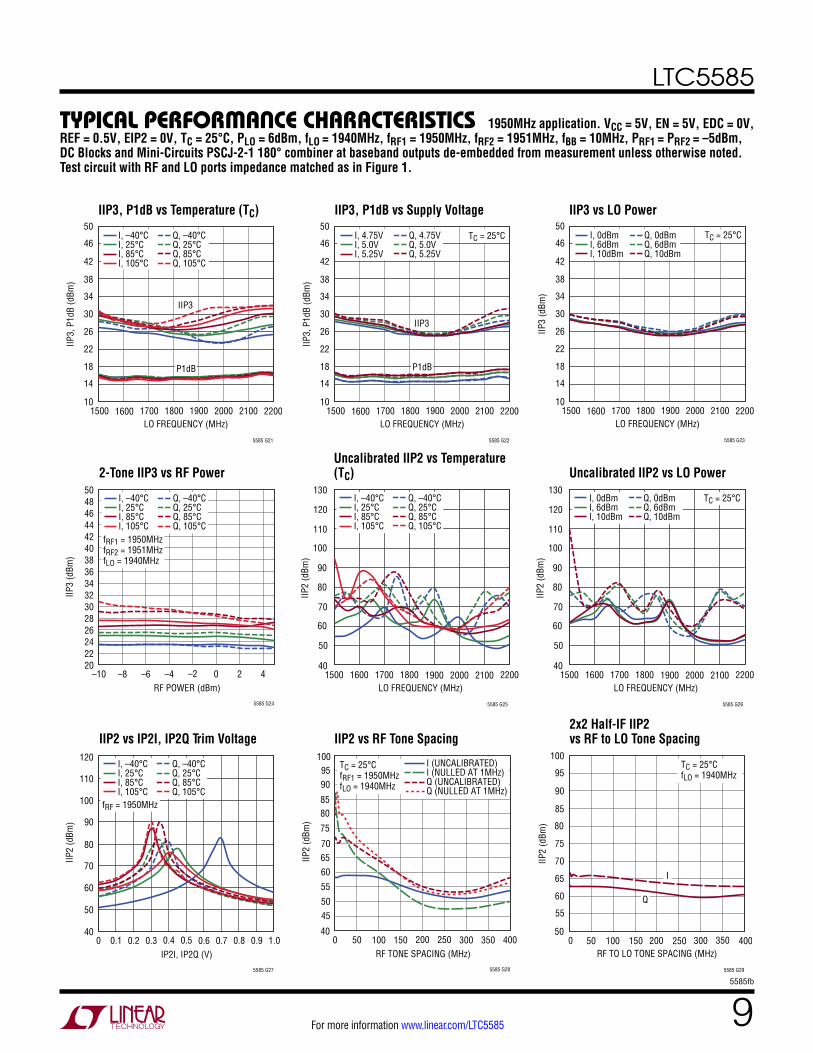
TYPICAL PERFORMANCE CHARACTERISTICS 1950MHz application. VCC = 5V, EN = 5V, EDC = 0V, REF = 0.5V, EIP2 = 0V, TC = 25°C, PLO = 6dBm, fLO = 1940MHz, fRF1 = 1950MHz, fRF2 = 1951MHz, fBB = 10MHz, PRF1 = PRF2 = –5dBm, DC Blocks and Mini-Circuits PSCJ-2-1 180° combiner at baseband outputs de-embedded from measurement unless otherwise noted. Test circuit with RF and LO ports impedance matched as in Figure 1.
2-Tone IIP3 vs RF Power
2x2 Half-IF IIP2 vs RF to LO Tone Spacing
Uncalibrated IIP2 vs Temperature (TC) Uncalibrated IIP2 vs LO Power
IIP2 vs IP2I, IP2Q Trim Voltage IIP2 vs RF Tone Spacing
IIP3, P1dB vs Temperature (TC) IIP3, P1dB vs Supply Voltage IIP3 vs LO Power
LO FREQUENCY (MHz)1500
10
IIP3,
P1d
B (d
Bm)
14
22
26
30
50
38
1700 1900 2000 2100
5585 G21
18
42
46
34
1600 1800 2200
I, –40°CI, 25°CI, 85°CI, 105°C
Q, –40°CQ, 25°CQ, 85°CQ, 105°C
IIP3
P1dB
LO FREQUENCY (MHz)1500
10
IIP3,
P1d
B (d
Bm)
14
22
26
30
50
38
1700 1900 2000 2100
5585 G22
18
42
46
34
1600 1800 2200
I, 4.75VI, 5.0VI, 5.25V
Q, 4.75VQ, 5.0VQ, 5.25V
TC = 25°C
IIP3
P1dB
LO FREQUENCY (MHz)1500
10
IIP3
(dBm
)
14
22
26
30
50
38
1700 1900 2000 2100
5585 G23
18
42
46
34
1600 1800 2200
I, 0dBmI, 6dBmI, 10dBm
Q, 0dBmQ, 6dBmQ, 10dBm
TC = 25°C
RF POWER (dBm)–10
IIP3
(dBm
) 38
44
504846
4042
3436
2830
2224
–4 0 2 4
5585 G24
32
26
20–8 –6 –2
I, –40°CI, 25°CI, 85°CI, 105°C
Q, –40°CQ, 25°CQ, 85°CQ, 105°C
fRF1 = 1950MHzfRF2 = 1951MHzfLO = 1940MHz
LO FREQUENCY (MHz)1500
40
IIP2
(dBm
)
50
70
80
90
1900
130
5585 G25
60
17001600 2000 21001800 2200
100
110
120I, –40°CI, 25°CI, 85°CI, 105°C
Q, –40°CQ, 25°CQ, 85°CQ, 105°C
LO FREQUENCY (MHz)1500
40
IIP2
(dBm
)
50
70
80
90
1900
130
5585 G26
60
17001600 2000 21001800 2200
100
110
120I, 0dBmI, 6dBmI, 10dBm
Q, 0dBmQ, 6dBmQ, 10dBm
TC = 25°C
IP2I, IP2Q (V)0
IIP2
(dBm
)
80
90
100
0.8 0.9
5585 G27
70
60
400.2 0.4 0.60.1 1.00.3 0.5 0.7
50
120
fRF = 1950MHz
110
I, –40°CI, 25°CI, 85°CI, 105°C
Q, –40°CQ, 25°CQ, 85°CQ, 105°C
RF TONE SPACING (MHz)0
IIP2
(dBm
)
70
85
90
400
5585 G28
6560
40100 200 30050 150 250 350
50
10095
80
75
55
45
I (UNCALIBRATED)I (NULLED AT 1MHz)Q (UNCALIBRATED)Q (NULLED AT 1MHz)
TC = 25°CfRF1 = 1950MHzfLO = 1940MHz
RF TO LO TONE SPACING (MHz)0
50
IIP2
(dBm
)
55
65
70
75
100
85
100 200 250
5585 G29
60
90
95
80
50 150 300 350 400
TC = 25°CfLO = 1940MHz
Q
I
LTC5585
105585fb
For more information www.linear.com/LTC5585
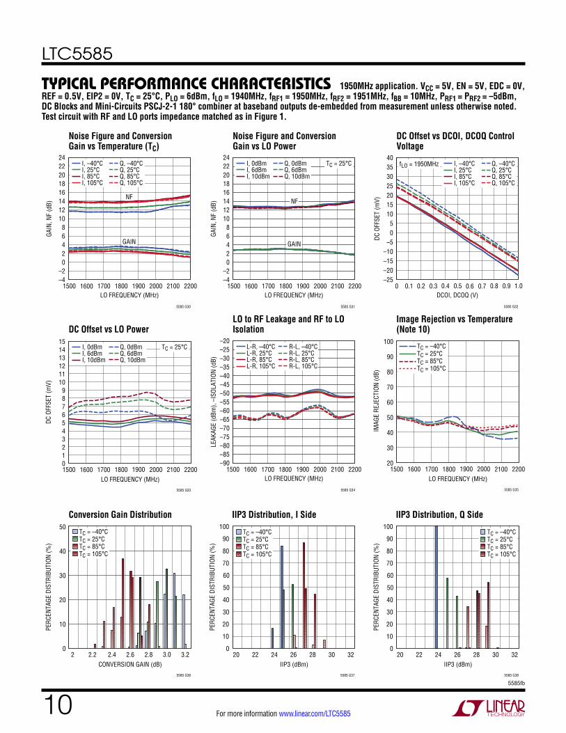
TYPICAL PERFORMANCE CHARACTERISTICS 1950MHz application. VCC = 5V, EN = 5V, EDC = 0V, REF = 0.5V, EIP2 = 0V, TC = 25°C, PLO = 6dBm, fLO = 1940MHz, fRF1 = 1950MHz, fRF2 = 1951MHz, fBB = 10MHz, PRF1 = PRF2 = –5dBm, DC Blocks and Mini-Circuits PSCJ-2-1 180° combiner at baseband outputs de-embedded from measurement unless otherwise noted. Test circuit with RF and LO ports impedance matched as in Figure 1.
Noise Figure and Conversion Gain vs Temperature (TC)
Noise Figure and Conversion Gain vs LO Power
DC Offset vs DCOI, DCOQ Control Voltage
LO to RF Leakage and RF to LO IsolationDC Offset vs LO Power
Image Rejection vs Temperature (Note 10)
LO FREQUENCY (MHz)1500
–4
GAIN
, NF
(dB)
0
4
8
24
16
1600 1800 1900 2000 2100
20
12
–2
2
6
22
14
18
10
1700 2200
5585 G30
NF
GAIN
I, –40°CI, 25°CI, 85°CI, 105°C
Q, –40°CQ, 25°CQ, 85°CQ, 105°C
LO FREQUENCY (MHz)1500
–4
GAIN
, NF
(dB)
0
4
8
24
16
1600 1800 1900 2000 2100
20
12
–2
2
6
22
14
18
10
1700 2200
5585 G31
I, 0dBmI, 6dBmI, 10dBm
Q, 0dBmQ, 6dBmQ, 10dBm
TC = 25°C
NF
GAIN
DCOI, DCOQ (V)0
–25
DC O
FFSE
T (m
V)
–20
–10–50
25303540
10
0.2 0.4
5585 G32
–15
1520
5
0.6 1.00.80.1 0.3 0.5 0.7 0.9
I, –40°CI, 25°CI, 85°CI, 105°C
Q, –40°CQ, 25°CQ, 85°CQ, 105°C
fLO = 1950MHz
LO FREQUENCY (MHz)1500
DC O
FFSE
T (m
V)
9
12
151413
1011
78
45
12
1800 2000 22002100
5585 G33
6
3
01600 1700 1900
I, 0dBmI, 6dBmI, 10dBm
Q, 0dBmQ, 6dBmQ, 10dBm
TC = 25°C
LO FREQUENCY (MHz)1500
–90
LEAK
AGE
(dBm
), –I
SOLA
TION
(dB)
–80
–70
–60
–20
–40
1600 1700 2000 2100
–30
–50
–85
–75
–65
–25
–45
–35
–55
1800 1900 2200
5585 G34
L-R, –40°CL-R, 25°CL-R, 85°CL-R, 105°C
R-L, –40°CR-L, 25°CR-L, 85°CR-L, 105°C
LO FREQUENCY (MHz)1500
IMAG
E RE
JECT
ION
(dB)
60
80
2200
5585 G35
40
201700 1900 21001600 1800 2000
100
50
70
30
90
TC = –40°CTC = 25°CTC = 85°CTC = 105°C
Conversion Gain Distribution IIP3 Distribution, I Side IIP3 Distribution, Q Side
CONVERSION GAIN (dB)2 2.2
PERC
ENTA
GE D
ISTR
IBUT
ION
(%)
20
30
5585 G36
10
02.4 2.6 2.8 3.0 3.2
50
40
TC = –40°CTC = 25°CTC = 85°CTC = 105°C
IIP3 (dBm)20
PERC
ENTA
GE D
ISTR
IBUT
ION
(%)
60
80
100
28
5585 G37
40
20
50
70
90
30
10
022 24 26 30 32
TC = –40°CTC = 25°CTC = 85°CTC = 105°C
IIP3 (dBm)20
PERC
ENTA
GE D
ISTR
IBUT
ION
(%)
60
80
100
28
5585 G38
40
20
50
70
90
30
10
022 24 26 30 32
TC = –40°CTC = 25°CTC = 85°CTC = 105°C
LTC5585
115585fb
For more information www.linear.com/LTC5585
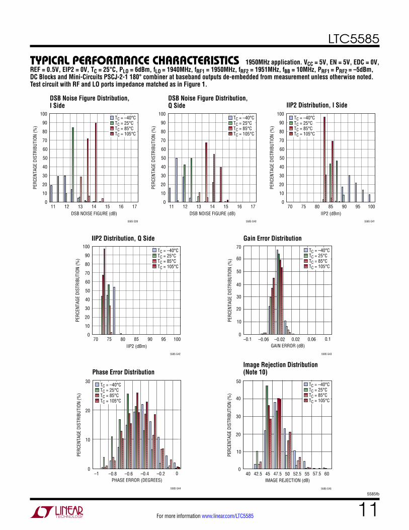
TYPICAL PERFORMANCE CHARACTERISTICS 1950MHz application. VCC = 5V, EN = 5V, EDC = 0V, REF = 0.5V, EIP2 = 0V, TC = 25°C, PLO = 6dBm, fLO = 1940MHz, fRF1 = 1950MHz, fRF2 = 1951MHz, fBB = 10MHz, PRF1 = PRF2 = –5dBm, DC Blocks and Mini-Circuits PSCJ-2-1 180° combiner at baseband outputs de-embedded from measurement unless otherwise noted. Test circuit with RF and LO ports impedance matched as in Figure 1.
Phase Error DistributionImage Rejection Distribution (Note 10)
DSB Noise Figure Distribution, I Side
DSB Noise Figure Distribution, Q Side IIP2 Distribution, I Side
IIP2 Distribution, Q Side Gain Error Distribution
DSB NOISE FIGURE (dB)11
PERC
ENTA
GE D
ISTR
IBUT
ION
(%)
60
80
100
15
5585 G39
40
20
50
70
90
30
10
012 13 14 16 17
TC = –40°CTC = 25°CTC = 85°CTC = 105°C
DSB NOISE FIGURE (dB)11
PERC
ENTA
GE D
ISTR
IBUT
ION
(%)
60
80
100
15
5585 G40
40
20
50
70
90
30
10
012 13 14 16 17
TC = –40°CTC = 25°CTC = 85°CTC = 105°C
IIP2 (dBm)70
PERC
ENTA
GE D
ISTR
IBUT
ION
(%)
60
80
100
90
5585 G41
40
20
50
70
90
30
10
075 80 85 95 100
TC = –40°CTC = 25°CTC = 85°CTC = 105°C
IIP2 (dBm)70
PERC
ENTA
GE D
ISTR
IBUT
ION
(%)
60
80
100
90
5585 G42
40
20
50
70
90
30
10
075 80 85 95 100
TC = –40°CTC = 25°CTC = 85°CTC = 105°C
GAIN ERROR (dB)–0.1
0
PERC
ENTA
GE D
ISTR
IBUT
ION
(%)
10
30
40
50
70
5585 G43
20
60
–0.02 0.1–0.06 0.02 0.06
TC = –40°CTC = 25°CTC = 85°CTC = 105°C
PHASE ERROR (DEGREES)–1
0
PERC
ENTA
GE D
ISTR
IBUT
ION
(%)
20
30
5585 G44
10
–0.6 0–0.8 –0.4 –0.2
TC = –40°CTC = 25°CTC = 85°CTC = 105°C
IMAGE REJECTION (dB)40
0
PERC
ENTA
GE D
ISTR
IBUT
ION
(%)
10
30
40
50
45 50 52.5 60
5585 G45
20
42.5 47.5 55 57.5
TC = –40°CTC = 25°CTC = 85°CTC = 105°C
LTC5585
125585fb
For more information www.linear.com/LTC5585
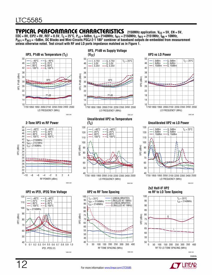
TYPICAL PERFORMANCE CHARACTERISTICS 2150MHz application. VCC = 5V, EN = 5V, EDC = 0V, EIP2 = 0V, REF = 0.5V, TC = 25°C, PLO = 6dBm, fLO = 2140MHz, fRF1 = 2150MHz, fRF2 = 2151MHz, fBB = 10MHz, PRF1 = PRF2 = –5dBm, DC Blocks and Mini-Circuits PSCJ-2-1 180° combiner at baseband outputs de-embedded from measurement unless otherwise noted. Test circuit with RF and LO ports impedance matched as in Figure 1.
IIP3, P1dB vs Temperature (TC)IIP3, P1dB vs Supply Voltage (VCC) IIP3 vs LO Power
LO FREQUENCY (MHz)1750
10
IIP3,
P1d
B (d
Bm)
14
22
26
30
50
38
1950 2150 2250
5585 G46
18
42
46
34
1850 2050 2350 2450 2550
I, –40°CI, 25°CI, 85°CI, 105°C
Q, –40°CQ, 25°CQ, 85°CQ, 105°C
IIP3
P1dB
LO FREQUENCY (MHz)1750
10
IIP3,
P1d
B (d
Bm)
14
22
26
30
50
38
1950 2150 2250
5585 G47
18
42
46
34
1850 2050 2350 2450 2550
I, 4.75VI, 5.0VI, 5.25V
Q, 4.75VQ, 5.0VQ, 5.25V
TC = 25°C
IIP3
P1dB
LO FREQUENCY (MHz)1750
10
IIP3
(dBm
)
14
22
26
30
50
38
1950 2150 2250
5585 G48
18
42
46
34
1850 2050 2350 2450 2550
I, 0dBmI, 6dBmI, 10dBm
Q, 0dBmQ, 6dBmQ, 10dBm
TC = 25°C
2-Tone IIP3 vs RF PowerUncalibrated IIP2 vs Temperature (TC) Uncalibrated IIP2 vs LO Power
RF POWER (dBm)–10
IIP3
(dBm
) 38
44
504846
4042
3436
2830
2224
–4 0 2 4
5585 G49
32
26
20–8 –6 –2
I, –40°CI, 25°CI, 85°CI, 105°C
Q, –40°CQ, 25°CQ, 85°CQ, 105°C
fRF1 = 2150MHzfRF2 = 2151MHzfLO = 2140MHz
LO FREQUENCY (MHz)1750
40
IIP2
(dBm
)
50
70
80
90
2150
130
5585 G50
60
19501850 2250 2350 24502050 2550
100
110
120I, –40°CI, 25°CI, 85°CI, 105°C
Q, –40°CQ, 25°CQ, 85°CQ, 105°C
LO FREQUENCY (MHz)1750
40
IIP2
(dBm
)
50
70
80
90
2150
130
5585 G51
60
19501850 2250 2350 24502050 2550
100
110
120I, 0dBmI, 6dBmI, 10dBm
Q, 0dBmQ, 6dBmQ, 10dBm
TC = 25°C
IIP2 vs IP2I, IP2Q Trim Voltage IIP2 vs RF Tone Spacing2x2 Half-IF IIP2 vs RF to LO Tone Spacing
IP2I, IP2Q (V)0
IIP2
(dBm
)
80
90
100
0.8 0.9
5585 G52
70
60
400.2 0.4 0.60.1 1.00.3 0.5 0.7
50
120
fRF = 2150MHz
110
I, –40°CI, 25°CI, 85°CI, 105°C
Q, –40°CQ, 25°CQ, 85°CQ, 105°C
RF TONE SPACING (MHz)0
IIP2
(dBm
)
70
85
90
400
5585 G53
6560
40100 200 30050 150 250 350
50
10095
80
75
55
45
I (UNCALIBRATED)I (NULLED AT 1MHz)Q (UNCALIBRATED)Q (NULLED AT 1MHz)
TC = 25°CfRF1 = 2150MHzfLO = 2140MHz
RF TO LO TONE SPACING (MHz)0
50
IIP2
(dBm
)
55
65
70
75
100
85
100 200 250
5585 G54
60
90
95
80
50 150 300 350 400
TC = 25°CfLO = 2140MHz
Q
I
LTC5585
135585fb
For more information www.linear.com/LTC5585
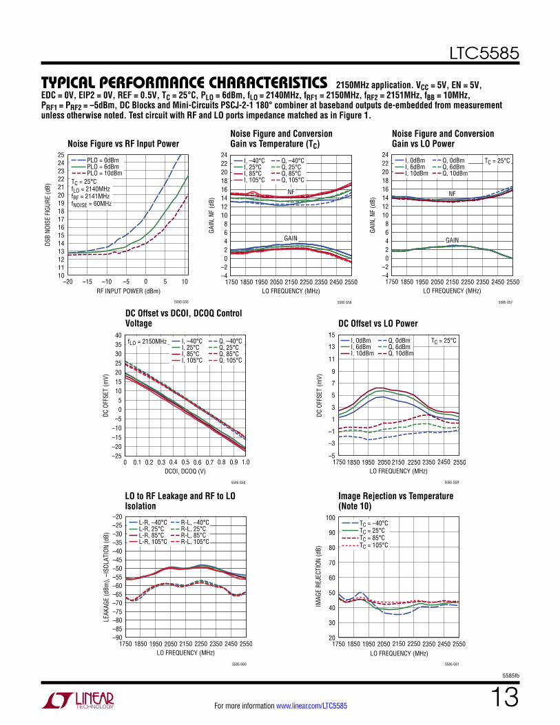
TYPICAL PERFORMANCE CHARACTERISTICS 2150MHz application. VCC = 5V, EN = 5V, EDC = 0V, EIP2 = 0V, REF = 0.5V, TC = 25°C, PLO = 6dBm, fLO = 2140MHz, fRF1 = 2150MHz, fRF2 = 2151MHz, fBB = 10MHz, PRF1 = PRF2 = –5dBm, DC Blocks and Mini-Circuits PSCJ-2-1 180° combiner at baseband outputs de-embedded from measurement unless otherwise noted. Test circuit with RF and LO ports impedance matched as in Figure 1.
DC Offset vs DCOI, DCOQ Control Voltage DC Offset vs LO Power
LO to RF Leakage and RF to LO Isolation
Image Rejection vs Temperature (Note 10)
Noise Figure vs RF Input PowerNoise Figure and Conversion Gain vs Temperature (TC)
Noise Figure and Conversion Gain vs LO Power
RF INPUT POWER (dBm)–20
DSB
NOIS
E FI
GURE
(dB)
19
22
252423
2021
1718
1415
1112
–5 5 10
5585 G55
16
13
10–15 –10 0
PLO = 0dBmPLO = 6dBmPLO = 10dBm
TC = 25°CfLO = 2140MHzfRF = 2141MHzfNOISE = 60MHz
LO FREQUENCY (MHz)1750 1850 1950 2050 2150 2250 2350 2450 2550
–4
GAIN
, NF
(dB)
0
4
8
24
16
20
12
–2
2
6
22
14
18
10
5585 G56
I, –40°CI, 25°CI, 85°CI, 105°C
Q, –40°CQ, 25°CQ, 85°CQ, 105°C
NF
GAIN
LO FREQUENCY (MHz)1750 1850
–4
GAIN
, NF
(dB)
0
4
8
24
16
1950 2050 2150 2250 2350 2450 2550
20
12
–2
2
6
22
14
18
10
5585 G57
I, 0dBmI, 6dBmI, 10dBm
Q, 0dBmQ, 6dBmQ, 10dBm
TC = 25°C
NF
GAIN
DCOI, DCOQ (V)0
–25
DC O
FFSE
T (m
V)
–20
–10–50
25303540
10
0.2 0.4
5585 G58
–15
1520
5
0.6 1.00.80.1 0.3 0.5 0.7 0.9
I, –40°CI, 25°CI, 85°CI, 105°C
Q, –40°CQ, 25°CQ, 85°CQ, 105°C
fLO = 2150MHz
LO FREQUENCY (MHz)1750
–5
DC O
FFSE
T (m
V)
–3
1
3
5
15
9
1950 2150 2250
5585 G59
–1
11
13
7
1850 2050 2350 2450 2550
I, 0dBmI, 6dBmI, 10dBm
Q, 0dBmQ, 6dBmQ, 10dBm
TC = 25°C
LO FREQUENCY (MHz)1750
–90
LEAK
AGE
(dBm
), –I
SOLA
TION
(dB)
–80
–70
–60
–20
–40
1850 1950 2250 2350 2450
–30
–50
–85
–75
–65
–25
–45
–35
–55
2050 2150 2550
5585 G60
L-R, –40°CL-R, 25°CL-R, 85°CL-R, 105°C
R-L, –40°CR-L, 25°CR-L, 85°CR-L, 105°C
LO FREQUENCY (MHz)1750
IMAG
E RE
JECT
ION
(dB)
60
80
2550
5585 G61
40
201950 2150 23501850 2050 2250 2450
100
50
70
30
90TC = –40°CTC = 25°CTC = 85°CTC = 105°C
LTC5585
145585fb
For more information www.linear.com/LTC5585
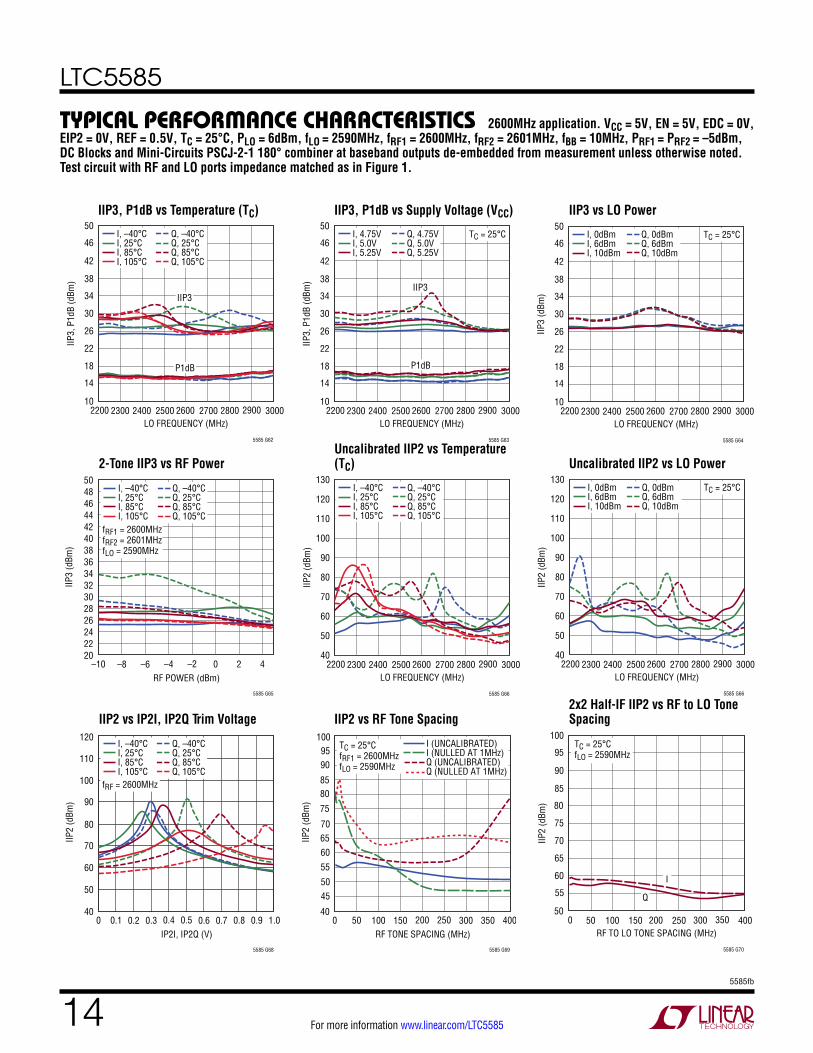
TYPICAL PERFORMANCE CHARACTERISTICS 2600MHz application. VCC = 5V, EN = 5V, EDC = 0V, EIP2 = 0V, REF = 0.5V, TC = 25°C, PLO = 6dBm, fLO = 2590MHz, fRF1 = 2600MHz, fRF2 = 2601MHz, fBB = 10MHz, PRF1 = PRF2 = –5dBm, DC Blocks and Mini-Circuits PSCJ-2-1 180° combiner at baseband outputs de-embedded from measurement unless otherwise noted. Test circuit with RF and LO ports impedance matched as in Figure 1.
2-Tone IIP3 vs RF Power Uncalibrated IIP2 vs LO PowerUncalibrated IIP2 vs Temperature (TC)
IIP2 vs IP2I, IP2Q Trim Voltage IIP2 vs RF Tone Spacing2x2 Half-IF IIP2 vs RF to LO Tone Spacing
IIP3, P1dB vs Temperature (TC) IIP3, P1dB vs Supply Voltage (VCC) IIP3 vs LO Power
LO FREQUENCY (MHz)2200
10
IIP3,
P1d
B (d
Bm)
14
22
26
30
50
38
2400 2600 2700
5585 G62
18
42
46
34
2300 2500 2800 2900 3000
I, –40°CI, 25°CI, 85°CI, 105°C
Q, –40°CQ, 25°CQ, 85°CQ, 105°C
IIP3
P1dB
LO FREQUENCY (MHz)2200
10
IIP3,
P1d
B (d
Bm)
14
22
26
30
50
38
2400 2600 2700
5585 G63
18
42
46
34
2300 2500 2800 2900 3000
I, 4.75VI, 5.0VI, 5.25V
Q, 4.75VQ, 5.0VQ, 5.25V
TC = 25°C
IIP3
P1dB
LO FREQUENCY (MHz)2200
10
IIP3
(dBm
)
14
22
26
30
50
38
2400 2600 2700
5585 G64
18
42
46
34
2300 2500 2800 2900 3000
I, 0dBmI, 6dBmI, 10dBm
Q, 0dBmQ, 6dBmQ, 10dBm
TC = 25°C
RF POWER (dBm)–10
IIP3
(dBm
) 38
44
504846
4042
3436
2830
2224
–4 0 2 4
5585 G65
32
26
20–8 –6 –2
I, –40°CI, 25°CI, 85°CI, 105°C
Q, –40°CQ, 25°CQ, 85°CQ, 105°C
fRF1 = 2600MHzfRF2 = 2601MHzfLO = 2590MHz
LO FREQUENCY (MHz)2200
40
IIP2
(dBm
)
50
70
80
90
130
100
2400 2600 2700
5585 G66
60
110
120
2300 2500 2800 2900 3000
I, –40°CI, 25°CI, 85°CI, 105°C
Q, –40°CQ, 25°CQ, 85°CQ, 105°C
LO FREQUENCY (MHz)2200
40
IIP2
(dBm
)
50
70
80
90
130
100
2400 2600 2700
5585 G66
60
110
120
2300 2500 2800 2900 3000
I, 0dBmI, 6dBmI, 10dBm
Q, 0dBmQ, 6dBmQ, 10dBm
TC = 25°C
IP2I, IP2Q (V)0
IIP2
(dBm
)
80
90
100
0.8 0.9
5585 G68
70
60
400.2 0.4 0.60.1 1.00.3 0.5 0.7
50
120
fRF = 2600MHz
110
I, –40°CI, 25°CI, 85°CI, 105°C
Q, –40°CQ, 25°CQ, 85°CQ, 105°C
RF TONE SPACING (MHz)0
IIP2
(dBm
)
70
85
90
400
5585 G69
6560
40100 200 30050 150 250 350
50
10095
80
75
55
45
I (UNCALIBRATED)I (NULLED AT 1MHz)Q (UNCALIBRATED)Q (NULLED AT 1MHz)
TC = 25°CfRF1 = 2600MHzfLO = 2590MHz
RF TO LO TONE SPACING (MHz)0
50
IIP2
(dBm
)
55
65
70
75
100
85
100 200 250
5585 G70
60
90
95
80
50 150 300 350 400
TC = 25°CfLO = 2590MHz
Q
I
LTC5585
155585fb
For more information www.linear.com/LTC5585
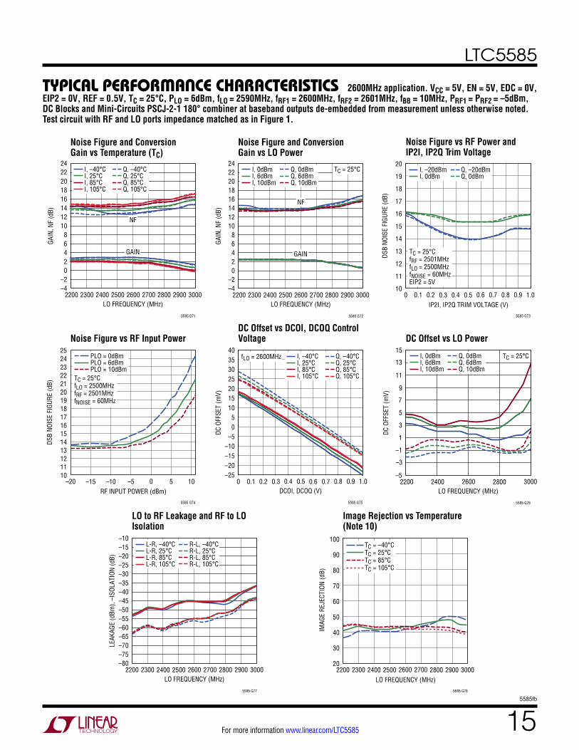
Noise Figure vs RF Power and IP2I, IP2Q Trim Voltage
DC Offset vs DCOI, DCOQ Control Voltage DC Offset vs LO Power
LO to RF Leakage and RF to LO Isolation
Image Rejection vs Temperature (Note 10)
Noise Figure and Conversion Gain vs LO Power
Noise Figure vs RF Input Power
Noise Figure and Conversion Gain vs Temperature (TC)
TYPICAL PERFORMANCE CHARACTERISTICS 2600MHz application. VCC = 5V, EN = 5V, EDC = 0V, EIP2 = 0V, REF = 0.5V, TC = 25°C, PLO = 6dBm, fLO = 2590MHz, fRF1 = 2600MHz, fRF2 = 2601MHz, fBB = 10MHz, PRF1 = PRF2 = –5dBm, DC Blocks and Mini-Circuits PSCJ-2-1 180° combiner at baseband outputs de-embedded from measurement unless otherwise noted. Test circuit with RF and LO ports impedance matched as in Figure 1.
LO FREQUENCY (MHz)2200 2300 2400 2500 2600 2700 2800 2900 3000
–4
GAIN
, NF
(dB)
0
4
8
24
16
20
12
–2
2
6
22
14
18
10
5585 G71
I, –40°CI, 25°CI, 85°CI, 105°C
Q, –40°CQ, 25°CQ, 85°CQ, 105°C
NF
GAIN
LO FREQUENCY (MHz)2200 2300 2400 2500 2600 2700 2800 2900 3000
–4
GAIN
, NF
(dB)
0
4
8
24
16
20
12
–2
2
6
22
14
18
10
5585 G72
I, 0dBmI, 6dBmI, 10dBm
Q, 0dBmQ, 6dBmQ, 10dBm
TC = 25°C
NF
GAIN
IP2I, IP2Q TRIM VOLTAGE (V)0
DSB
NOIS
E FI
GURE
(dB)
16
18
20
0.8
5585 G73
14
12
15
17
19
13
11
100.20.1 0.40.3 0.6 0.7 0.90.5 1.0
I, –20dBmI, 0dBm
Q, –20dBmQ, 0dBm
TC = 25°CfRF = 2501MHzfLO = 2500MHzfNOISE = 60MHzEIP2 = 5V
RF INPUT POWER (dBm)–20
DSB
NOIS
E FI
GURE
(dB)
19
22
252423
2021
1718
1415
1112
–5 5 10
5585 G74
16
13
10–15 –10 0
PLO = 0dBmPLO = 6dBmPLO = 10dBm
TC = 25°CfLO = 2500MHzfRF = 2501MHzfNOISE = 60MHz
DCOI, DCOQ (V)0
–25
DC O
FFSE
T (m
V)
–20
–10–50
25303540
10
0.2 0.4
5585 G75
–15
1520
5
0.6 1.00.80.1 0.3 0.5 0.7 0.9
I, –40°CI, 25°CI, 85°CI, 105°C
Q, –40°CQ, 25°CQ, 85°CQ, 105°C
fLO = 2600MHz
LO FREQUENCY (MHz)2200
–5
DC O
FFSE
T (m
V)
–3
1
3
5
15
9
2400 2600
5585 G76
–1
11
13
7
2800 3000
TC = 25°CI, 0dBmI, 6dBmI, 10dBm
Q, 0dBmQ, 6dBmQ, 10dBm
LO FREQUENCY (MHz)2200
–80
LEAK
AGE
(dBm
), –I
SOLA
TION
(dB)
–70
–60
–50
–10
–30
2300 2400 2700 2800 2900
–20
–40
–75
–65
–55
–15
–35
–25
–45
2500 2600 3000
5585 G77
L-R, –40°CL-R, 25°CL-R, 85°CL-R, 105°C
R-L, –40°CR-L, 25°CR-L, 85°CR-L, 105°C
LO FREQUENCY (MHz)2200
IMAG
E RE
JECT
ION
(dB)
60
80
3000
5585 G78
40
202400 2600 28002300 2500 2700 2900
100
50
70
30
90TC = –40°CTC = 25°CTC = 85°CTC = 105°C
LTC5585
165585fb
For more information www.linear.com/LTC5585
PIN FUNCTIONSIP2Q, IP2I (Pin 1, Pin 4): IIP2 Adjustment Analog Control Voltage Input for Q and I Channel. A decoupling capacitor is recommended on this pin. A low output resistance volt-age source is recommended for driving these pins. These pins should be left floating if unused.
DCOQ, DCOI (Pin 2, Pin 3): DC Offset Analog Control Voltage Input for Q and I Channel. A decoupling capaci-tor is recommended on this pin. A low output resistance voltage source is recommended for driving these pins. These pins should be left floating if unused.
RF (Pin 5): RF Input. External matching is used to obtain good return loss across the RF input frequency range. The RF pin is internally shorted to ground through internal transformer windings. The RF pin should be DC-blocked with a 1000pF coupling capacitor.
GND (Pins 6, 8, 13, 14, Exposed Pad Pin 25): Ground. These pins must be soldered to the RF ground plane on the circuit board. The backside exposed pad ground con-nection should have a low inductance connection and good thermal contact to the printed circuit board ground plane using many through-hole vias. See Figures 2 and 3.
EN (Pin 7): Enable Pin. When the voltage on the EN pin is a logic high, the chip is completely turned on; the chip is completely turned off for a logic low. An internal 200k pull-down resistor ensures the chip remains disabled if there is no connection to the pin (open-circuit condition).
VBIAS (Pin 9): This pin can be pulled to ground through a resistor to lower the current consumption of the chip. See Applications Information.
VCC (Pin 10): Positive Supply Pin. This pin should be bypassed with shunt 1000pF and 1µF capacitors.
EDC (Pin 11): DC Offset Adjustment Mode Enable Pin. When the voltage on the EDC pin is a logic high, the DC offset control circuitry is enabled. The circuitry is disabled for a logic low. An internal 200k pull-down resistor ensures the circuitry remains disabled if there is no connection to the pin (open-circuit condition).
EIP2 (Pin 12): IP2 Offset Adjustment Mode Enable Pin. When the voltage on the EIP2 pin is a logic high, the IP2 adjustment circuitry is enabled. The circuitry is disabled for a logic low. An internal 200k pull-down resistor ensures the circuitry remains disabled if there is no connection to the pin (open-circuit condition).
LO+,LO– (Pin 15, Pin 16): LO Inputs. External matching is required to obtain good return loss across the LO input frequency range. Can be driven single ended or differen-tially with an external transformer. The LO pins should be DC-blocked with a 1000pF coupling capacitor.
VCAP, CMQ, CMI (Pin 17, Pin 18, Pin 19): Common Mode Bypass Capacitor Pins. It is recommended that CMI and CMQ be connected to VCAP through 0.1µF capacitors. Nothing else should be connected to VCAP since it is con-nected to VCC inside the chip.
I+, I–, Q+, Q– (Pin 23, Pin 22, Pin 21, Pin 20): Differential Baseband Output Pins for the I Channel and Q Channel. The DC bias point is VCC – 1.5V for each pin. These pins must have an external 100Ω or an inductor pull-up to VCC.
REF (Pin 24): Voltage Reference Input for Analog Control Voltage Pins. A decoupling capacitor is recommended on this pin. A low output resistance voltage source is recommended for driving this pin. This pin should be left floating if unused.
LTC5585
175585fb
For more information www.linear.com/LTC5585
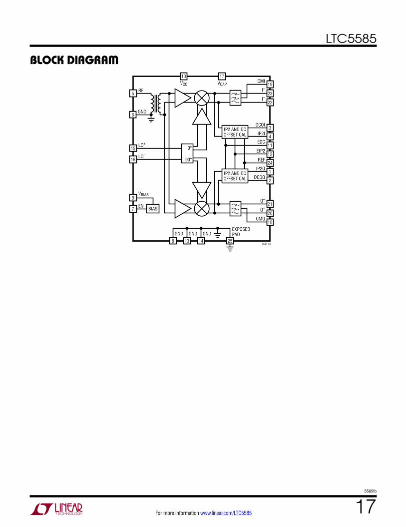
BLOCK DIAGRAM
RF
GND
0°
90°
BIAS
IP2 AND DCOFFSET CAL
VCC VCAPCMI
I+
I–
IP2 AND DCOFFSET CAL
23
19
22
5
Q+
Q–
CMQ20
21
18
EDC
EIP2
REF12
11
24
DCOI3
IP2I4
IP2Q1
DCOQ2
6
LO+15
LO–16
EN
GND
7
GND GND
5585 BD
EXPOSEDPAD
VBIAS9
258 13 14
10 17
LTC5585
185585fb
For more information www.linear.com/LTC5585
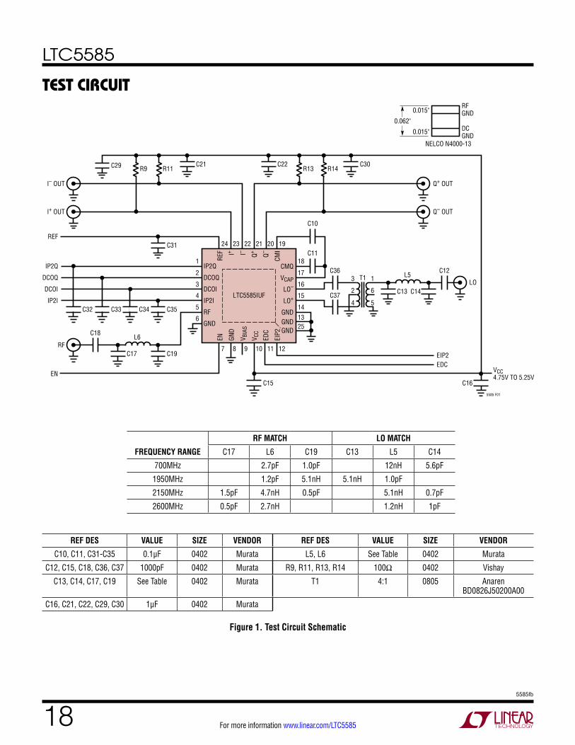
TEST CIRCUIT
FREQUENCY RANGE
RF MATCH LO MATCH
C17 L6 C19 C13 L5 C14
700MHz 2.7pF 1.0pF 12nH 5.6pF
1950MHz 1.2pF 5.1nH 5.1nH 1.0pF
2150MHz 1.5pF 4.7nH 0.5pF 5.1nH 0.7pF
2600MHz 0.5pF 2.7nH 1.2nH 1pF
REF DES VALUE SIZE VENDOR REF DES VALUE SIZE VENDOR
C10, C11, C31-C35 0.1μF 0402 Murata L5, L6 See Table 0402 Murata
C12, C15, C18, C36, C37 1000pF 0402 Murata R9, R11, R13, R14 100Ω 0402 Vishay
C13, C14, C17, C19 See Table 0402 Murata T1 4:1 0805 Anaren BD0826J50200A00
C16, C21, C22, C29, C30 1μF 0402 Murata
Figure 1. Test Circuit Schematic
24 23 22 21 20 19
7
C35
8 9 10 11 12
6
5
4
3
2
1
1325
14
15
16
17
18C11
IP2Q
DCOQ
DCOI
IP2I
RF
GND
IP2Q
DCOQ
DCOI
IP2I
CMQ
VCAP
LO–
LO+
GNDGNDGND
REF I+ I– Q+ Q–
CMI
EN GND
V BIA
S
V CC
EDC
EIP2
LTC5585IUF
C363 T1
2
4
1
6
5
C12
C37
C10
C31
C21R11
C22 C30
C13 C14LO
EIP2EDC
C16
5585 F01
VCC4.75V TO 5.25V
C15
C19
L6
C17
C18
C34C33
C29
C32
RF
I+ OUT
I– OUT
Q– OUT
Q+ OUT
EN
REF
RFGND0.015"
0.015"
0.062"
NELCO N4000-13
DCGND
L5
R13R9 R14
LTC5585
195585fb
For more information www.linear.com/LTC5585
APPLICATIONS INFORMATION
TEST CIRCUIT
The LTC5585 is an IQ demodulator designed for high dynamic range receiver applications. It consists of RF transconductance amplifiers, I/Q mixers, quadrature LO amplifiers, IIP2 and DC offset correction circuitry, and bias circuitry.
Operation
As shown in the Block Diagram for the LTC5585, the RF signal is applied to the inputs of the RF transconductor V-to-I converters and is then demodulated into I/Q baseband signals using quadrature LO signals which are internally generated by a precision 90° phase shifter. The demodulated I/Q signals are lowpass filtered on-chip with a –3dB bandwidth of 530MHz. The differential outputs of the I-channel and Q-channel are well matched in amplitude and their phases are 90° apart.
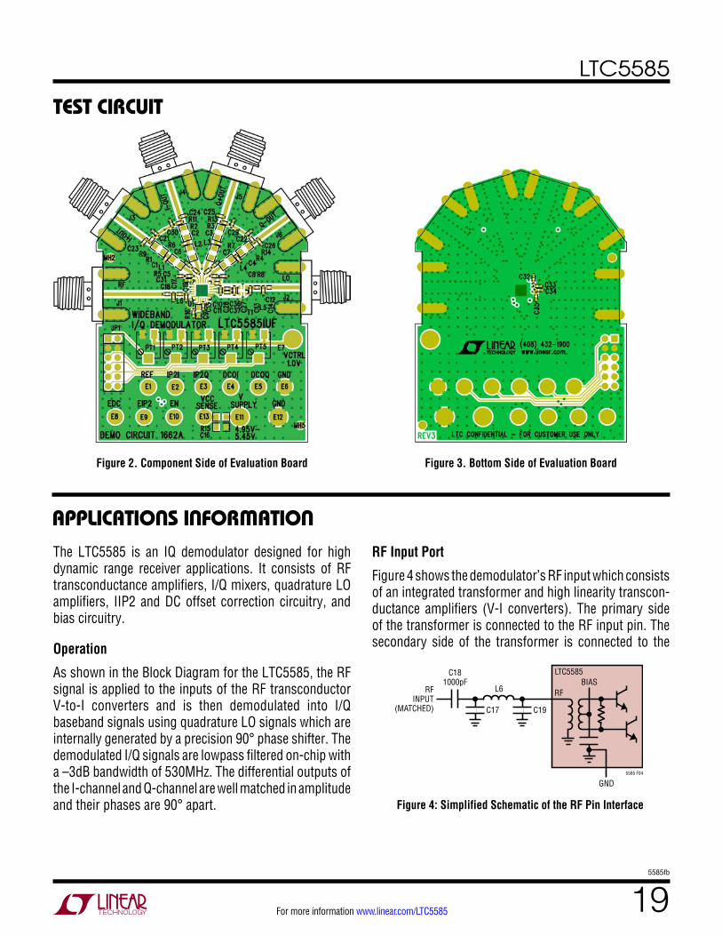
Figure 2. Component Side of Evaluation Board Figure 3. Bottom Side of Evaluation Board
RF Input Port
Figure 4 shows the demodulator’s RF input which consists of an integrated transformer and high linearity transcon-ductance amplifiers (V-I converters). The primary side of the transformer is connected to the RF input pin. The secondary side of the transformer is connected to the
C19C17
RFBIAS
L6
C181000pF
RFINPUT
(MATCHED)
GND5585 F04
LTC5585
Figure 4: Simplified Schematic of the RF Pin Interface
LTC5585
205585fb
For more information www.linear.com/LTC5585
APPLICATIONS INFORMATIONdifferential inputs of the transconductance amplifiers. External DC voltage should not be applied to the RF input pin. DC current flowing into the primary side of the trans-former may cause damage to the integrated transformer. A series DC blocking capacitor should be used to couple the RF input pin to the RF signal source.
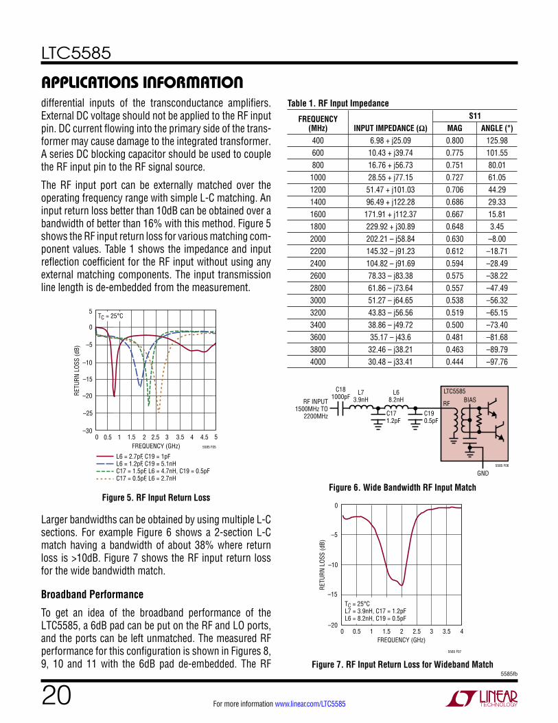
The RF input port can be externally matched over the operating frequency range with simple L-C matching. An input return loss better than 10dB can be obtained over a bandwidth of better than 16% with this method. Figure 5 shows the RF input return loss for various matching com-ponent values. Table 1 shows the impedance and input reflection coefficient for the RF input without using any external matching components. The input transmission line length is de-embedded from the measurement.
Larger bandwidths can be obtained by using multiple L-C sections. For example Figure 6 shows a 2-section L-C match having a bandwidth of about 38% where return loss is >10dB. Figure 7 shows the RF input return loss for the wide bandwidth match.
Broadband Performance
To get an idea of the broadband performance of the LTC5585, a 6dB pad can be put on the RF and LO ports, and the ports can be left unmatched. The measured RF performance for this configuration is shown in Figures 8, 9, 10 and 11 with the 6dB pad de-embedded. The RF
Figure 5. RF Input Return Loss
Figure 7. RF Input Return Loss for Wideband Match
Table 1. RF Input Impedance
FREQUENCY (MHz) INPUT IMPEDANCE (Ω)
S11MAG ANGLE (°)
400 6.98 + j25.09 0.800 125.98600 10.43 + j39.74 0.775 101.55800 16.76 + j56.73 0.751 80.01
1000 28.55 + j77.15 0.727 61.051200 51.47 + j101.03 0.706 44.291400 96.49 + j122.28 0.686 29.331600 171.91 + j112.37 0.667 15.811800 229.92 + j30.89 0.648 3.452000 202.21 – j58.84 0.630 –8.002200 145.32 – j91.23 0.612 –18.712400 104.82 – j91.69 0.594 –28.492600 78.33 – j83.38 0.575 –38.222800 61.86 – j73.64 0.557 –47.493000 51.27 – j64.65 0.538 –56.323200 43.83 – j56.56 0.519 –65.153400 38.86 – j49.72 0.500 –73.403600 35.17 – j43.6 0.481 –81.683800 32.46 – j38.21 0.463 –89.794000 30.48 – j33.41 0.444 –97.76
C190.5pF
C171.2pF
L68.2nH RF BIAS
C181000pF
RF INPUT1500MHz TO
2200MHz
GND5585 F06
LTC5585L73.9nH
Figure 6. Wide Bandwidth RF Input Match
FREQUENCY (GHz)0
–30
RETU
RN L
OSS
(dB)
–25
–15
–10
–5
5
0.5 2.5 3.55585 F05
–20
0
2 4.5 51 1.5 3 4
L6 = 2.7pF, C19 = 1pFL6 = 1.2pF, C19 = 5.1nHC17 = 1.5pF, L6 = 4.7nH, C19 = 0.5pFC17 = 0.5pF, L6 = 2.7nH
TC = 25°C
FREQUENCY (GHz)0
–20
RETU
RN L
OSS
(dB)
–15
–10
–5
0
0.5 1 1.5 2
5585 F07
2.5 3 3.5 4
TC = 25°CL7 = 3.9nH, C17 = 1.2pFL6 = 8.2nH, C19 = 0.5pF
LTC5585
215585fb
For more information www.linear.com/LTC5585
APPLICATIONS INFORMATION
tone spacing is 1MHz, and fLO is 10MHz lower than fRF. The conversion gain is lower than under the impedance matched condition, and correspondingly the P1dB, IIP3, and NF are higher. As shown, the part can be used at frequencies outside its specified operating range with reduced conversion gain and higher NF.
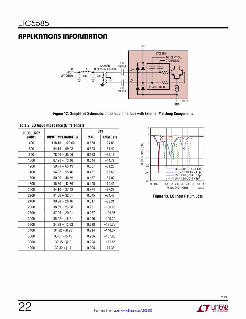
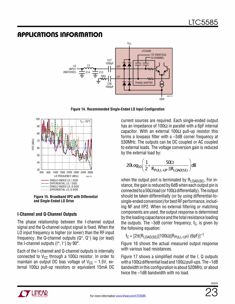
LO Input Port
The demodulator’s LO input interface is shown in Fig-ure 12. The input consists of a high precision quadrature phase shifter which generates 0° and 90° phase shifted LO signals for the LO buffer amplifiers to drive the I/Q mixers. DC blocking capacitors are required on the LO+
and LO– inputs.
Figure 8. Broadband IIP3 and IP1dB
Figure 11. Broadband Image RejectionFigure 9. Broadband IIP2
Figure 10. Broadband NF and Gain
The differential LO input impedance and S parameters with the input transmission lines and balun de-embedded are listed in Table 2.
Figure 13 shows LO input return loss using the ANAREN BD0826J50200A00 4:1 balun with various matching component values.
For optimum IIP2 and large-signal NF performance the LO inputs should be driven differentially with a 4:1 balun such as the ANAREN BD0826J50200A00 or BD2425J50200AHF. As shown in Figure 14, the LO input can also be driven single-ended from either the LO+ or LO– input. The unused port should be DC-blocked and terminated with a 50Ω load. Figure 15 compares the uncalibrated IIP2 performance of single ended versus differential LO drive.
LO FREQUENCY (MHz)400
10
IIP3,
P1d
B (d
Bm)
14
22
26
30
50
38
1400 2400 2900 3400
5585 F08
18
42
46
34
900 1900 3900
I, –40°CI, 25°CI, 85°CI, 105°C
Q, –40°CQ, 25°CQ, 85°CQ, 105°C
IIP3
P1dB
LO FREQUENCY (MHz)400
30
IIP2
(dBm
)
40
60
70
80
130
100
1400 2400 2900 3400
5585 F09
50
110
120
90
900 1900 3900
I, –40°CI, 25°CI, 85°CI, 105°C
Q, –40°CQ, 25°CQ, 85°CQ, 105°C
LO FREQUENCY (MHz)
–4
GAIN
, NF
(dB)
0–2
68
101214
201816
30
24
1400 2400 2900 3400
5585 F10
24
2628
22
900 1900 3900
I, –40°CI, 25°CI, 85°CI, 105°C
Q, –40°CQ, 25°CQ, 85°CQ, 105°C
NF
GAIN
LO FREQUENCY (MHz)500
IMAG
E RE
JECT
ION
(dB)
60
80
4000
5585 F11
40
201500 2500 35001000 2000 3000
100
50
70
30
90TC = –40°CTC = 25°CTC = 85°CTC = 105°C
LTC5585
225585fb
For more information www.linear.com/LTC5585
APPLICATIONS INFORMATION
Figure 12. Simplified Schematic of LO Input Interface with External Matching Components
TO IDENTICALQ-CHANNEL
PHASE SHIFTER
LTC5585
VCC
LO+
C371000pF
LOINPUT
(MATCHED) C13
C361000pF
ANARENBD0826J50200A00
LO–
GND5585 F12
C14
L5
Table 2. LO Input Impedance (Differential)
FREQUENCY (MHz) INPUT IMPEDANCE (Ω)
S11
MAG ANGLE (°)
400 118.18 – j120.02 0.668 –24.89
600 94.18 – j99.93 0.623 –31.42
800 78.00 – j85.06 0.583 –38.17
1000 67.21 – j73.16 0.544 –44.79
1200 59.71 – j63.49 0.507 –51.25
1400 54.22 – j55.46 0.471 –57.63
1600 50.06 – j48.59 0.437 –64.02
1800 46.80 – j42.69 0.405 –70.49
2000 44.10 – j37.42 0.374 –77.28
2200 41.86 – j32.61 0.345 –84.47
2400 39.98 – j28.16 0.317 –92.21
2600 38.39 – j23.98 0.291 –100.65
2800 37.05 – j20.01 0.267 –109.95
3000 35.92 – j16.21 0.246 –120.29
3200 34.99 – j12.53 0.228 –131.76
3400 34.22 – j8.95 0.214 –144.37
3600 33.61 – j5.45 0.206 –157.88
3800 33.15 – j2.0 0.204 –171.85
4000 32.82 + j1.4 0.208 174.35
Figure 13. LO Input Return Loss
FREQUENCY (GHz)0
–30
RETU
RN L
OSS
(dB)
–25
–15
–10
–5
5
0.5 2.5 3.55585 F13
–20
0
2 4.5 51 1.5 3 4
L5 = 12nH, C14 = 5.6pFC13 = 5.1nH, L5 = 1.0pF L5 = 5.1nH, C14 = 0.7pFL5 = 1.2nH, C14 = 1pF
LTC5585
235585fb
For more information www.linear.com/LTC5585
APPLICATIONS INFORMATION
I-Channel and Q-Channel Outputs
The phase relationship between the I-channel output signal and the Q-channel output signal is fixed. When the LO input frequency is higher (or lower) than the RF input frequency, the Q-channel outputs (Q+, Q–) lag (or lead) the I-channel outputs (I+, I–) by 90°.
Each of the I-channel and Q-channel outputs is internally connected to VCC through a 100Ω resistor. In order to maintain an output DC bias voltage of VCC – 1.5V, ex-ternal 100Ω pull-up resistors or equivalent 15mA DC
current sources are required. Each single-ended output has an impedance of 100Ω in parallel with a 6pF internal capacitor. With an external 100Ω pull-up resistor this forms a lowpass filter with a –3dB corner frequency at 530MHz. The outputs can be DC coupled or AC coupled to external loads. The voltage conversion gain is reduced by the external load by:
20Log10
12
+50Ω
RPULL-UP ||RLOAD(SE)
dB
when the output port is terminated by RLOAD(SE). For in-stance, the gain is reduced by 6dB when each output pin is connected to a 50Ω load (or 100Ω differentially). The output should be taken differentially (or by using differential-to-single-ended conversion) for best RF performance, includ-ing NF and IIP2. When no external filtering or matching components are used, the output response is determined by the loading capacitance and the total resistance loading the outputs. The –3dB corner frequency, fC, is given by the following equation:
fC = [2π(RLOAD(SE)||100Ω||RPULL-UP) (6pF)]–1
Figure 16 shows the actual measured output response with various load resistances.
Figure 17 shows a simplified model of the I, Q outputs with a 100Ω differential load and 100Ω pull-ups. The –1dB bandwidth in this configuration is about 520MHz, or about twice the –1dB bandwidth with no load.
TO IDENTICALQ-CHANNEL
PHASE SHIFTER
LTC5585
VCC
LO+
C371000pF
50Ω
L5LOINPUT
(MATCHED) C13
C361000pF
LO–
GND5585 F14
C14
Figure 14. Recommended Single-Ended LO Input Configuration
Figure 15. Broadband IIP2 with Differential and Single-Ended LO Drive
LO FREQUENCY (MHz)400
30
IIP2
(dBm
)
40
60
70
80
100
1400 2400 2900 34005585 F15
50
90
900 1900 3900
SINGLE-ENDED LO, I SIDEDIFFERENTIAL LO, I SIDESINGLE-ENDED LO, Q SIDEDIFFERENTIAL LO, Q SIDE
TC = 25°C
LTC5585
245585fb
For more information www.linear.com/LTC5585
Figure 16. Conversion Gain Baseband Output Response with RLOAD(DIFF) = 100Ω, 200Ω, 400Ω and 1k and RPULL-UP = 100Ω
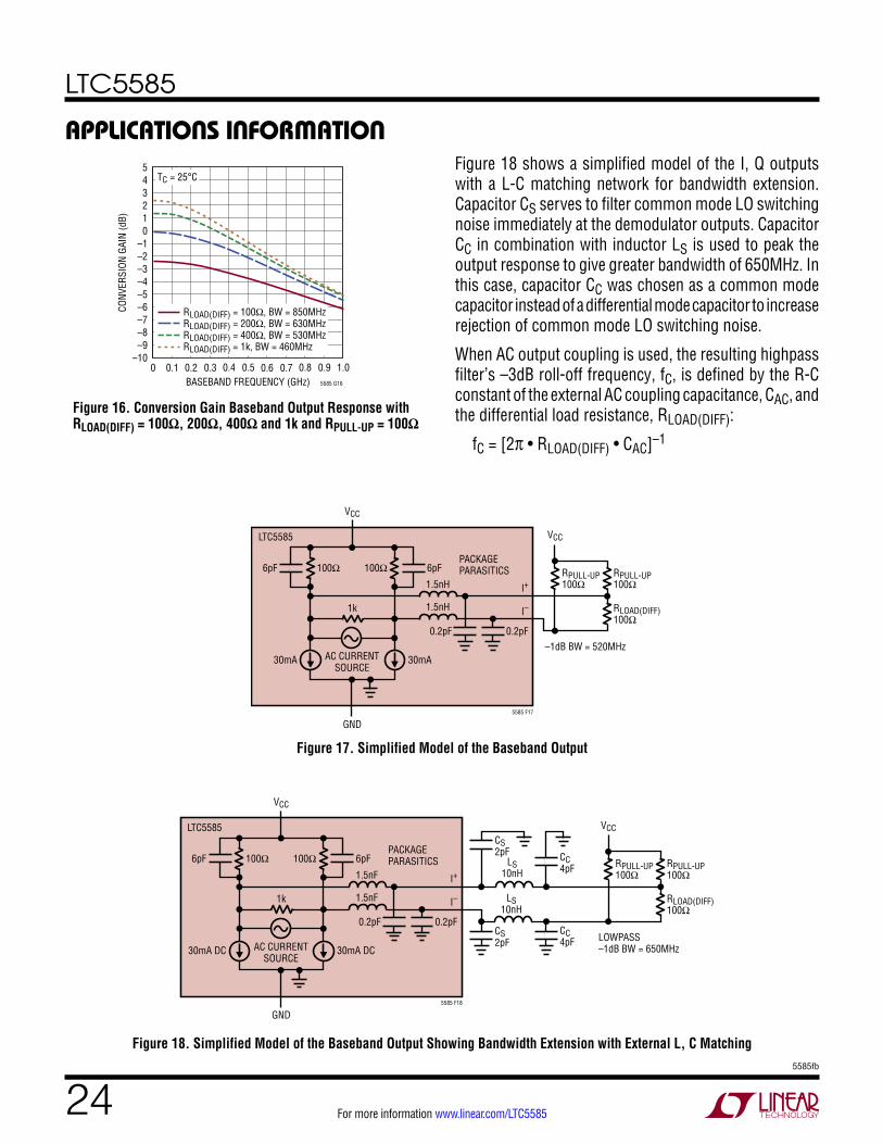
APPLICATIONS INFORMATIONFigure 18 shows a simplified model of the I, Q outputs with a L-C matching network for bandwidth extension. Capacitor CS serves to filter common mode LO switching noise immediately at the demodulator outputs. Capacitor CC in combination with inductor LS is used to peak the output response to give greater bandwidth of 650MHz. In this case, capacitor CC was chosen as a common mode capacitor instead of a differential mode capacitor to increase rejection of common mode LO switching noise.
When AC output coupling is used, the resulting highpass filter’s –3dB roll-off frequency, fC, is defined by the R-C constant of the external AC coupling capacitance, CAC, and the differential load resistance, RLOAD(DIFF):
fC = [2π • RLOAD(DIFF) • CAC]–1
Figure 17. Simplified Model of the Baseband Output
Figure 18. Simplified Model of the Baseband Output Showing Bandwidth Extension with External L, C Matching
100Ω
LTC5585
100Ω6pF 6pF
0.2pF
I+
I–
0.2pF
5585 F17
RLOAD(DIFF)100Ω
–1dB BW = 520MHz
1.5nH
VCC
VCC
GND
1k
AC CURRENTSOURCE
1.5nH
30mA30mA
RPULL-UP100Ω
RPULL-UP100Ω
PACKAGEPARASITICS
100Ω
LTC5585
100Ω6pF 6pF
0.2pF
I+
I–
0.2pFCS2pF
CS2pF CC
4pF
CC4pF
LS10nH
LS10nH
5585 F18
RLOAD(DIFF)100Ω
LOWPASS–1dB BW = 650MHz
1.5nF
VCC
VCC
GND
1k
AC CURRENTSOURCE
1.5nF
30mA DC30mA DC
RPULL-UP100Ω
RPULL-UP100Ω
PACKAGEPARASITICS
BASEBAND FREQUENCY (GHz)0
–10
CONV
ERSI
ON G
AIN
(dB)
–8–9
–7
–5–4–3
01
32
45
0.2 0.45585 G16
–6
–1–2
0.6 1.00.80.1 0.3 0.5 0.7 0.9
TC = 25°C
RLOAD(DIFF) = 100Ω, BW = 850MHzRLOAD(DIFF) = 200Ω, BW = 630MHzRLOAD(DIFF) = 400Ω, BW = 530MHzRLOAD(DIFF) = 1k, BW = 460MHz
LTC5585
255585fb
For more information www.linear.com/LTC5585
APPLICATIONS INFORMATIONCare should be taken when the demodulator’s outputs are DC coupled to the external load to make sure that the I/Q mixers are biased properly. If the current drain from the outputs exceeds about 6mA, there can be significant degradation of the linearity performance. Keeping the com-mon mode output voltage of the demodulator above 3.15V, with a 5V supply, will ensure optimum performance. Each output can sink no more than 30mA when the outputs are connected to an external load with a DC voltage higher than VCC – 1.5V.
In order to achieve the best IIP2 performance, it is im-portant to minimize high frequency coupling among the baseband outputs, RF port, and LO port. Although it may increase layout complexity, routing the baseband output traces on the backside of the PCB can improve uncalibrated IIP2 performance. Figure 19 shows the alternate layout having the baseband outputs on the backside of the PCB.
Analog Control Voltage Pins
Figure 20 shows the equivalent circuit for the DCOI, DCOQ, IP2I, and IP2Q pins. Internal temperature compensated 62.5μA current sources keep these pins biased at a nominal 500mV through 8k resistors. A low impedance voltage source with a source resistance of less than 200Ω is recommended to drive these pins.
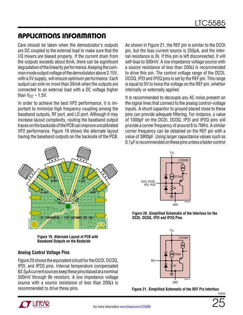
Figure 19. Alternate Layout of PCB with Baseband Outputs on the Backside
Figure 20. Simplified Schematic of the Interface for the DCOI, DCOQ, IP2I and IP2Q Pins
Figure 21. Simplified Schematic of the REF Pin Interface
GND5585 F20
VCC
8k
DCOI, DCOQ,IP2I, IP2Q
62.5µA
LTC5585
GND5585 F21
VCC
2k
REF
250µA
LTC5585
As shown in Figure 21, the REF pin is similar to the DCOI pin, but the bias current source is 250µA, and the inter-nal resistance is 2k. If this pin is left disconnected, it will self-bias to 500mV. A low impedance voltage source with a source resistance of less than 200Ω is recommended to drive this pin. The control voltage range of the DCOI, DCOQ, IP2I and IP2Q pins is set by the REF pin. This range is equal to 0V to twice the voltage on the REF pin, whether internally or externally applied.
It is recommended to decouple any AC noise present on the signal lines that connect to the analog control-voltage inputs. A shunt capacitor to ground placed close to these pins can provide adequate filtering. For instance, a value of 1000pF on the DCOI, DCOQ, IP2I and IP2Q pins will provide a corner frequency of around 6 to 7MHz. A similar corner frequency can be obtained on the REF pin with a value of 3900pF. Using larger capacitance values such as 0.1µF is recommended on these pins unless a faster control
LTC5585
265585fb
For more information www.linear.com/LTC5585
APPLICATIONS INFORMATIONresponse is needed. Figure 22 shows the input response –3dB bandwidth for the pins versus shunt capacitance when driven from a 50Ω source.
Figure 22. Input Response Bandwidth for the DCOI, DCOQ, IP2I and IP2Q Pins
SAMPLE ANDHOLD
DCAVERAGINGLOWPASS
FILTER
DSP
DAC
ADC
DCOI
fLO = 1950MHz 5585 F23
LNA
BPF
LTC5585
1-DMINIMIZATIONALGORITHM
Figure 23. Block Diagram of a Receiver with a DSP Feedback Loop for DC Offset Adjustment
FREQUENCY (MHz)0
RESP
ONSE
(dB)
–4
–2
0
165585 F22
–6
–8
–5
–3
–1
–7
–9
–1042 86 12 14 1810 20
DCOI, DCOQ; C = 470pFDCOI, DCOQ; C = 1000pFIP2I, IP2Q; C = 1000pF
TC = 25°C
DC Offset Adjustment Circuitry
Any sources of LO leakage to the RF input of a direct conversion receiver will contribute to the DC offsets of its baseband outputs. The LTC5585 features DC offset adjustment circuitry to reduce such effects. When the EDC pin is a logic high the circuitry is enabled and the resulting DC offset adjustment range is typically ±20mV. In a typical direct conversion receiver application, DC offset calibration will be done periodically at a time when no receive data is present and when the receiver DC levels have sufficiently settled.
DC Offset Adjustment Example
Figure 23 shows a typical direct conversion receive path having a DSP feedback path for DC offset adjustment. Any sources of LO leakage to the RF input of the LTC5585 demodulator will contribute to the DC offset of the receiver. This includes both static and dynamic DC offsets. If the coupling is static in nature due to fixed board-level leakage paths, the resulting DC offset does not typically need to be adjusted at a high repetition rate. Dynamic DC offsets due to transmitter transient leakage or antenna reflection can be much harder to correct for and will require a faster update rate from the DSP.
LO leakage into the RF port of the demodulator causes a DC offset at the baseband outputs which is then multiplied by the gain in the baseband path. The usable ADC voltage window will be reduced by the amplified DC offset, result-ing in lower dynamic range. Using DSP, this DC offset value can be averaged and sampled at a given update rate and then a 1D minimization algorithm can be applied before a new DCOI or DCOQ control signal is generated to minimize the offset. The 1-D minimization algorithm can be implemented in many ways such as golden-section search, backtracking, or Newton’s method.
IM2 Adjustment Circuitry
The LTC5585 also contains circuitry for the independent adjustment of IM2 levels on the I and Q channels. When the EIP2 pin is a logic high, this circuitry is enabled and the IP2I and IP2Q analog control voltage inputs are able
LTC5585
275585fb
For more information www.linear.com/LTC5585
APPLICATIONS INFORMATIONto adjust the IM2 level. The IM2 level can be effectively minimized over a large range of the baseband bandwidth. The circuitry has an effective baseband frequency upper limit of about 200MHz. Any IM2 component that falls in this frequency range can be minimized. Beyond this frequency, the gain of the IM2 correction amplifier falls off appreciably and the circuit no longer improves IP2 performance. The lower baseband frequency limit of the IM2 adjustment circuitry is set by the common mode reference decoupling capacitor at the CMI and CMQ pins. Below this frequency the circuit can not minimize the IM2 component.
Figure 24 shows the CMI (and identical CMQ) pin interface. These pins have an internal 40pF decoupling capacitance to VCC, to provide a reference for the IP2 adjustment cir-cuitry. The lower 3dB frequency limit, fC, of the circuitry is set by the following equation:
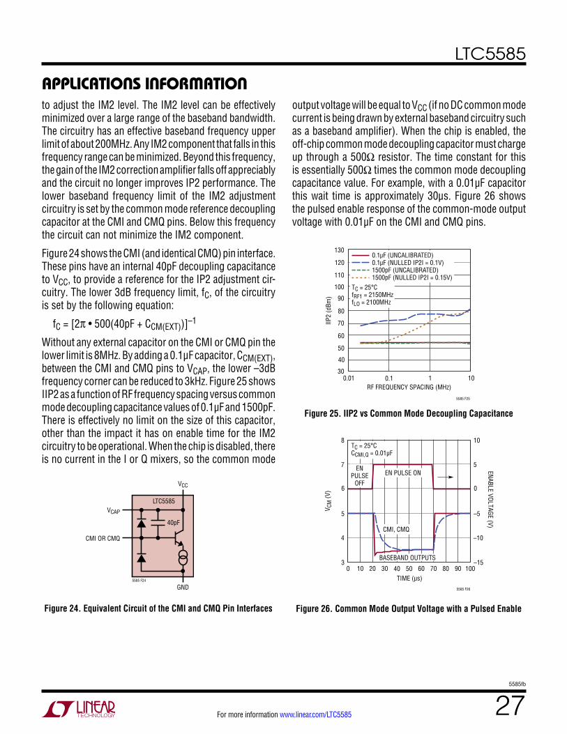
fC = [2π • 500(40pF + CCM(EXT))]–1
Without any external capacitor on the CMI or CMQ pin the lower limit is 8MHz. By adding a 0.1μF capacitor, CCM(EXT), between the CMI and CMQ pins to VCAP, the lower –3dB frequency corner can be reduced to 3kHz. Figure 25 shows IIP2 as a function of RF frequency spacing versus common mode decoupling capacitance values of 0.1µF and 1500pF. There is effectively no limit on the size of this capacitor, other than the impact it has on enable time for the IM2 circuitry to be operational. When the chip is disabled, there is no current in the I or Q mixers, so the common mode
output voltage will be equal to VCC (if no DC common mode current is being drawn by external baseband circuitry such as a baseband amplifier). When the chip is enabled, the off-chip common mode decoupling capacitor must charge up through a 500Ω resistor. The time constant for this is essentially 500Ω times the common mode decoupling capacitance value. For example, with a 0.01µF capacitor this wait time is approximately 30μs. Figure 26 shows the pulsed enable response of the common-mode output voltage with 0.01µF on the CMI and CMQ pins.
Figure 24. Equivalent Circuit of the CMI and CMQ Pin Interfaces Figure 26. Common Mode Output Voltage with a Pulsed Enable
Figure 25. IIP2 vs Common Mode Decoupling Capacitance
GND5585 F24
VCC
VCAP
CMI OR CMQ
40pF
LTC5585
RF FREQUENCY SPACING (MHz)0.01
30
IIP2
(dBm
)
50
60
70
80
90
100
0.1 1
5585 F25
110
120
130
TC = 25°CfRF1 = 2150MHzfLO = 2100MHz
40
10
0.1µF (UNCALIBRATED)0.1µF (NULLED IP2I = 0.1V)1500pF (UNCALIBRATED)1500pF (NULLED IP2I = 0.15V)
TIME (µs)0
V CM
(V)
ENABLE VOLTAGE (V)
6
7
8
80
5585 F26
5
4
3
0
5
10
–5
–10
–1510 20 30 40 50 60 70 90 100
TC = 25°CCCMI,Q = 0.01µF
ENPULSE
OFF
EN PULSE ON
CMI, CMQ
BASEBAND OUTPUTS
LTC5585
285585fb
For more information www.linear.com/LTC5585
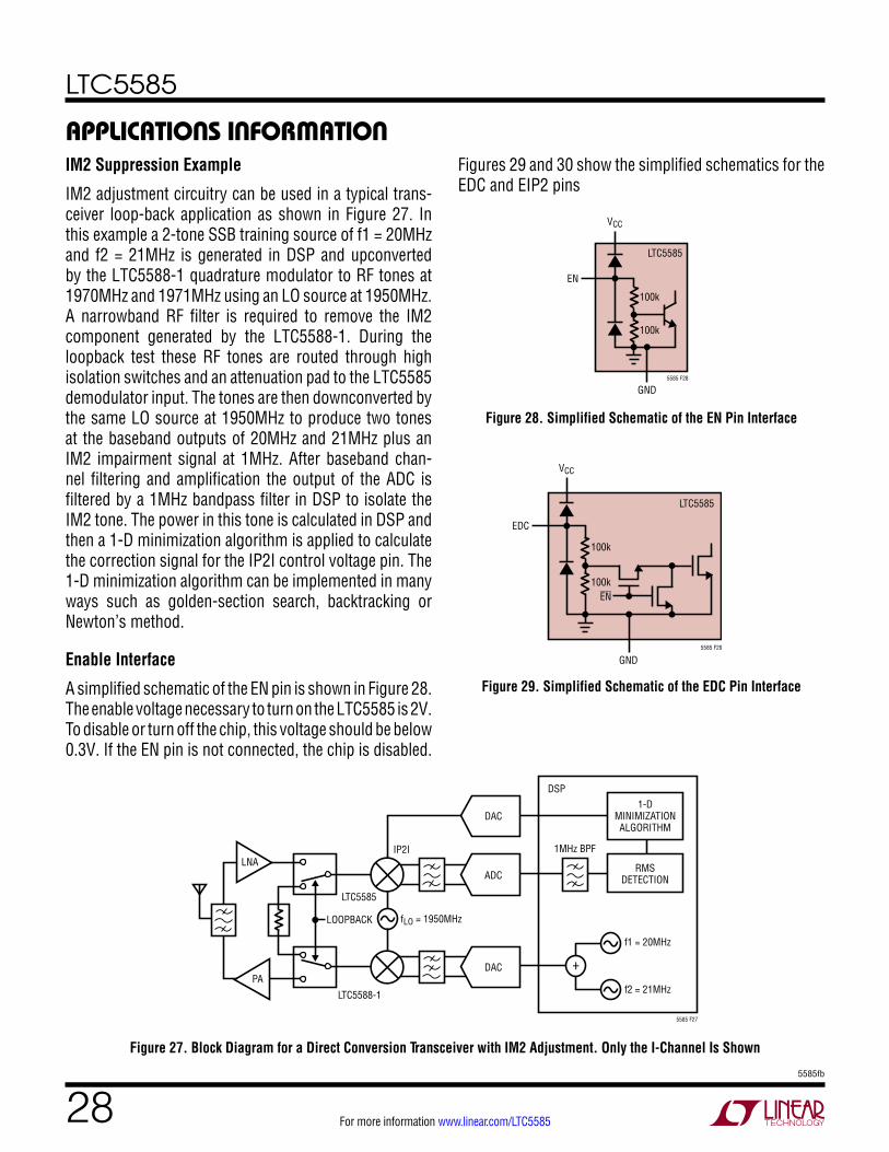
IM2 Suppression Example
IM2 adjustment circuitry can be used in a typical trans-ceiver loop-back application as shown in Figure 27. In this example a 2-tone SSB training source of f1 = 20MHz and f2 = 21MHz is generated in DSP and upconverted by the LTC5588-1 quadrature modulator to RF tones at 1970MHz and 1971MHz using an LO source at 1950MHz. A narrowband RF filter is required to remove the IM2 component generated by the LTC5588-1. During the loopback test these RF tones are routed through high isolation switches and an attenuation pad to the LTC5585 demodulator input. The tones are then downconverted by the same LO source at 1950MHz to produce two tones at the baseband outputs of 20MHz and 21MHz plus an IM2 impairment signal at 1MHz. After baseband chan-nel filtering and amplification the output of the ADC is filtered by a 1MHz bandpass filter in DSP to isolate the IM2 tone. The power in this tone is calculated in DSP and then a 1-D minimization algorithm is applied to calculate the correction signal for the IP2I control voltage pin. The 1-D minimization algorithm can be implemented in many ways such as golden-section search, backtracking or Newton’s method.
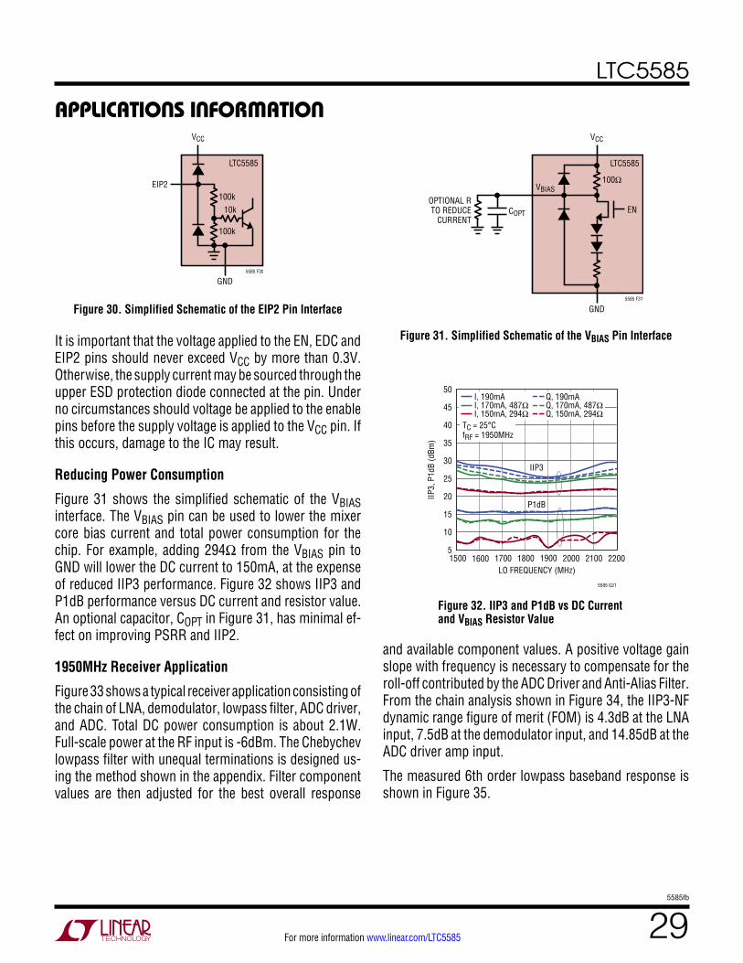
Enable Interface
A simplified schematic of the EN pin is shown in Figure 28. The enable voltage necessary to turn on the LTC5585 is 2V. To disable or turn off the chip, this voltage should be below 0.3V. If the EN pin is not connected, the chip is disabled.
APPLICATIONS INFORMATION
Figure 27. Block Diagram for a Direct Conversion Transceiver with IM2 Adjustment. Only the I-Channel Is Shown
Figure 28. Simplified Schematic of the EN Pin Interface
Figure 29. Simplified Schematic of the EDC Pin Interface
RMSDETECTION
1MHz BPF
DSP
DAC
ADC
IP2I
fLO = 1950MHz
f1 = 20MHz
f2 = 21MHz
5585 F27
LNA
LTC5585
LOOPBACK
LTC5588-1
1-DMINIMIZATIONALGORITHM
DACPA
+
100k
EN
LTC5585
GND5585 F28
VCC
100k
EN100k
100k
EDC
LTC5585
5585 F29
VCC
GND
Figures 29 and 30 show the simplified schematics for the EDC and EIP2 pins
LTC5585
295585fb
For more information www.linear.com/LTC5585
APPLICATIONS INFORMATION
It is important that the voltage applied to the EN, EDC and EIP2 pins should never exceed VCC by more than 0.3V. Otherwise, the supply current may be sourced through the upper ESD protection diode connected at the pin. Under no circumstances should voltage be applied to the enable pins before the supply voltage is applied to the VCC pin. If this occurs, damage to the IC may result.
Reducing Power Consumption
Figure 31 shows the simplified schematic of the VBIAS interface. The VBIAS pin can be used to lower the mixer core bias current and total power consumption for the chip. For example, adding 294Ω from the VBIAS pin to GND will lower the DC current to 150mA, at the expense of reduced IIP3 performance. Figure 32 shows IIP3 and P1dB performance versus DC current and resistor value. An optional capacitor, COPT in Figure 31, has minimal ef-fect on improving PSRR and IIP2.
1950MHz Receiver Application
Figure 33 shows a typical receiver application consisting of the chain of LNA, demodulator, lowpass filter, ADC driver, and ADC. Total DC power consumption is about 2.1W. Full-scale power at the RF input is -6dBm. The Chebychev lowpass filter with unequal terminations is designed us-ing the method shown in the appendix. Filter component values are then adjusted for the best overall response
Figure 32. IIP3 and P1dB vs DC Current and VBIAS Resistor Value
EN
VCC
GND5585 F31
100ΩVBIAS
COPT
OPTIONAL RTO REDUCE
CURRENT
LTC5585
Figure 31. Simplified Schematic of the VBIAS Pin Interface
100k
EIP2
LTC5585
GND5585 F30
VCC
100k10k
Figure 30. Simplified Schematic of the EIP2 Pin Interface
LO FREQUENCY (MHz)15005
IIP3,
P1d
B (d
Bm)
15
20
25
50
35
1700 1900 2000 2100
5585 G21
10
40
45
30
1600 1800 2200
I, 190mAI, 170mA, 487ΩI, 150mA, 294Ω
Q, 190mAQ, 170mA, 487ΩQ, 150mA, 294Ω
TC = 25°CfRF = 1950MHz
IIP3
P1dB
and available component values. A positive voltage gain slope with frequency is necessary to compensate for the roll-off contributed by the ADC Driver and Anti-Alias Filter. From the chain analysis shown in Figure 34, the IIP3-NF dynamic range figure of merit (FOM) is 4.3dB at the LNA input, 7.5dB at the demodulator input, and 14.85dB at the ADC driver amp input.
The measured 6th order lowpass baseband response is shown in Figure 35.
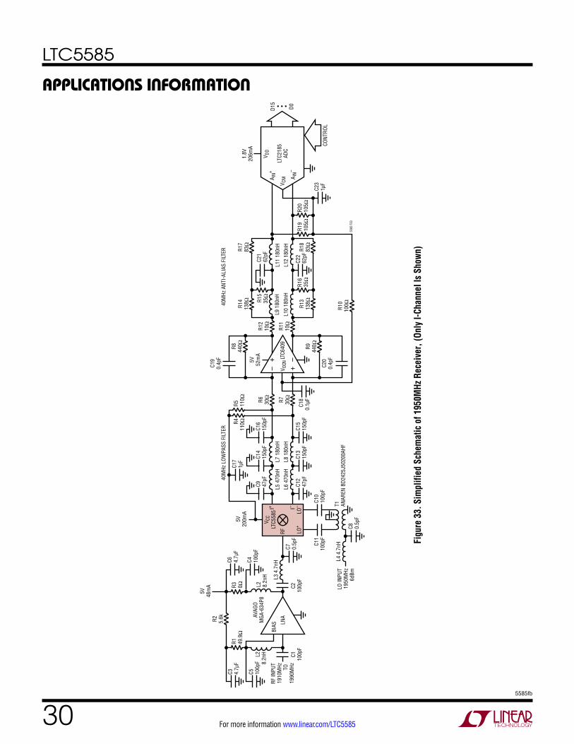
LTC5585
305585fb
For more information www.linear.com/LTC5585
APPLICATIONS INFORMATION
D15
D0
CONT
ROL
V CM
V DD
LTC2
185
ADC
1.8V
206m
A
5V20
0mA
5V48
mA
A IN+
A IN–
R20
105Ω
C22
62pF
C21
62pF
R19
105Ω
R16
35Ω
R15
35Ω
R5 110Ω
R411
0Ω
C23
1µF
5585
F33
R18
83Ω
R17
83Ω
R10
100Ω
R12
10Ω
R8 440Ω R9 440Ω
R7 30Ω
R2 5.6k
R6 30Ω
R11
10Ω
R13
138Ω
R14
138Ω
5V52
mA
C19
0.4p
F
C20
0.4p
F
C18
0.1µ
F
L12
180n
H
L11
180n
H
L8 1
80nH
L7 1
80nH
40M
Hz L
OWPA
SS F
ILTE
R40
MHz
ANT
I-ALI
AS F
ILTE
R
L6 4
70nH
L3 4
.7nH
AVAG
OM
GA-6
34P8
L2 8.2n
H
L4 4
.7nH
T1
ANAR
EN B
D242
5J50
200A
HF
L5 4
70nH
L10
180n
H
L9 1
80nH
• • •
C15
150p
F
C16
150p
F
C17
1µF
R3 0ΩR1 49
.9Ω
–
–+
+V O
CNLT
C640
9
C13
150p
F
C14
150p
F
C12
47pF
C10
100p
FC1
110
0pF
LO IN
PUT
1950
MHz
6dBm
C9 47pF
L28.
2nH
C7 0.5p
FC2
100p
FC1
100p
F
RF IN
PUT
1910
MHz TO
19
90M
Hz
C4 100p
FC5 10
0pF
C3 4.7µ
FC6 4.
7µF
C8 0.5p
F
I+V C
C
I–
RF
LO–
LO+LT
C558
5
LNA
BIAS
Figu
re 3
3. S
impl
ified
Sch
emat
ic o
f 195
0MHz
Rec
eive
r, (O
nly
I-Cha
nnel
Is S
how
n)
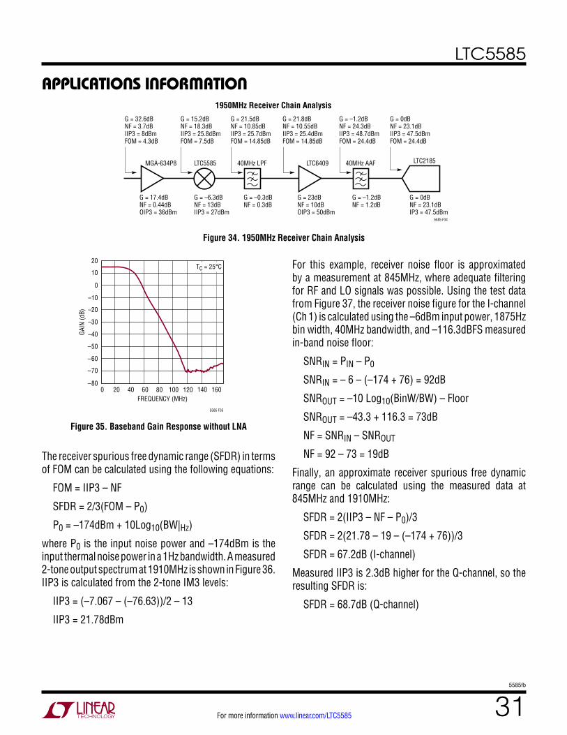
LTC5585
315585fb
For more information www.linear.com/LTC5585
APPLICATIONS INFORMATION
Figure 34. 1950MHz Receiver Chain Analysis
LTC2185
5585 F34
40MHz AAFLTC6409
G = 0dBNF = 23.1dBIP3 = 47.5dBm
G = –1.2dBNF = 1.2dB
G = 0dBNF = 23.1dBIIP3 = 47.5dBmFOM = 24.4dB
G = –1.2dBNF = 24.3dBIIP3 = 48.7dBmFOM = 24.4dB
40MHz LPF
1950MHz Receiver Chain Analysis
LTC5585
G = –0.3dBNF = 0.3dB
G = –6.3dBNF = 13dBIIP3 = 27dBm
G = 21.5dBNF = 10.85dBIIP3 = 25.7dBmFOM = 14.85dB
G = 15.2dBNF = 18.3dBIIP3 = 25.8dBmFOM = 7.5dB
G = 21.8dBNF = 10.55dBIIP3 = 25.4dBmFOM = 14.85dB
G = 23dBNF = 10dBOIP3 = 50dBm
MGA-634P8
G = 32.6dBNF = 3.7dBIIP3 = 8dBmFOM = 4.3dB
G = 17.4dBNF = 0.44dBOIP3 = 36dBm
The receiver spurious free dynamic range (SFDR) in terms of FOM can be calculated using the following equations:
FOM = IIP3 – NF
SFDR = 2/3(FOM – P0)
P0 = –174dBm + 10Log10(BW|Hz)
where P0 is the input noise power and –174dBm is the input thermal noise power in a 1Hz bandwidth. A measured 2-tone output spectrum at 1910MHz is shown in Figure 36. IIP3 is calculated from the 2-tone IM3 levels:
IIP3 = (–7.067 – (–76.63))/2 – 13
IIP3 = 21.78dBm
Figure 35. Baseband Gain Response without LNA
For this example, receiver noise floor is approximated by a measurement at 845MHz, where adequate filtering for RF and LO signals was possible. Using the test data from Figure 37, the receiver noise figure for the I-channel (Ch 1) is calculated using the –6dBm input power, 1875Hz bin width, 40MHz bandwidth, and –116.3dBFS measured in-band noise floor:
SNRIN = PIN – P0
SNRIN = – 6 – (–174 + 76) = 92dB
SNROUT = –10 Log10(BinW/BW) – Floor
SNROUT = –43.3 + 116.3 = 73dB
NF = SNRIN – SNROUT
NF = 92 – 73 = 19dB
Finally, an approximate receiver spurious free dynamic range can be calculated using the measured data at 845MHz and 1910MHz:
SFDR = 2(IIP3 – NF – P0)/3
SFDR = 2(21.78 – 19 – (–174 + 76))/3
SFDR = 67.2dB (I-channel)
Measured IIP3 is 2.3dB higher for the Q-channel, so the resulting SFDR is:
SFDR = 68.7dB (Q-channel)
FREQUENCY (MHz)0
–80
GAIN
(dB)
–70
–50
–40
–30
20
–10
40 80 100
5585 F35
–60
0
10
–20
20 60 120 140 160
TC = 25°C
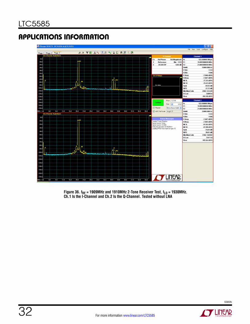
LTC5585
325585fb
For more information www.linear.com/LTC5585
APPLICATIONS INFORMATION
Figure 36. fRF = 1909MHz and 1910MHz 2-Tone Receiver Test, fLO = 1930MHz. Ch.1 Is the I-Channel and Ch.2 Is the Q-Channel. Tested without LNA
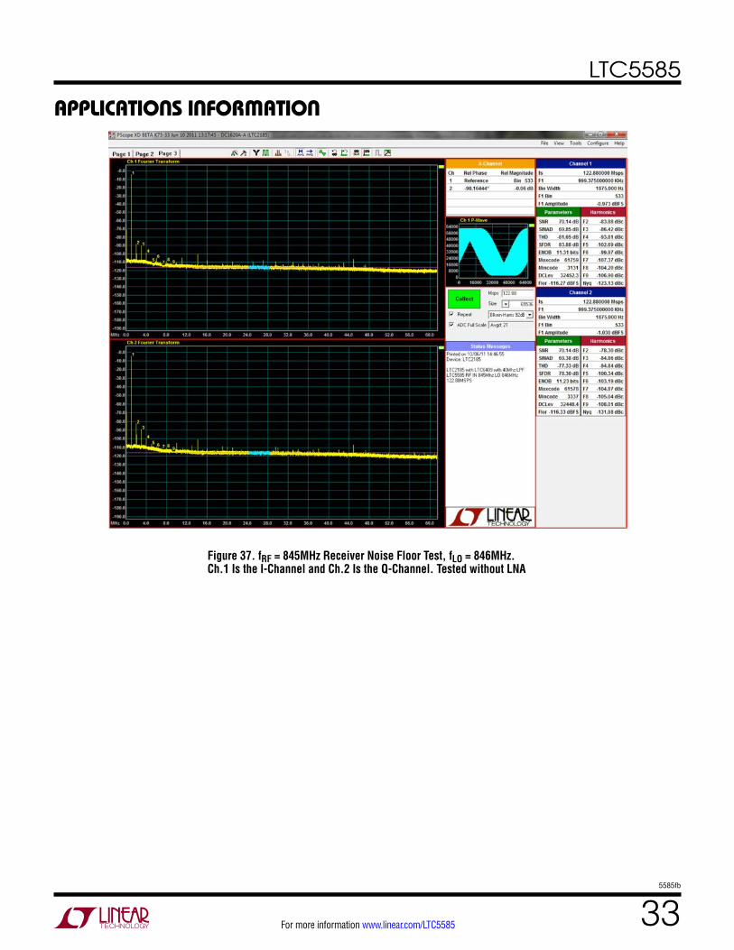
LTC5585
335585fb
For more information www.linear.com/LTC5585
APPLICATIONS INFORMATION
Figure 37. fRF = 845MHz Receiver Noise Floor Test, fLO = 846MHz. Ch.1 Is the I-Channel and Ch.2 Is the Q-Channel. Tested without LNA
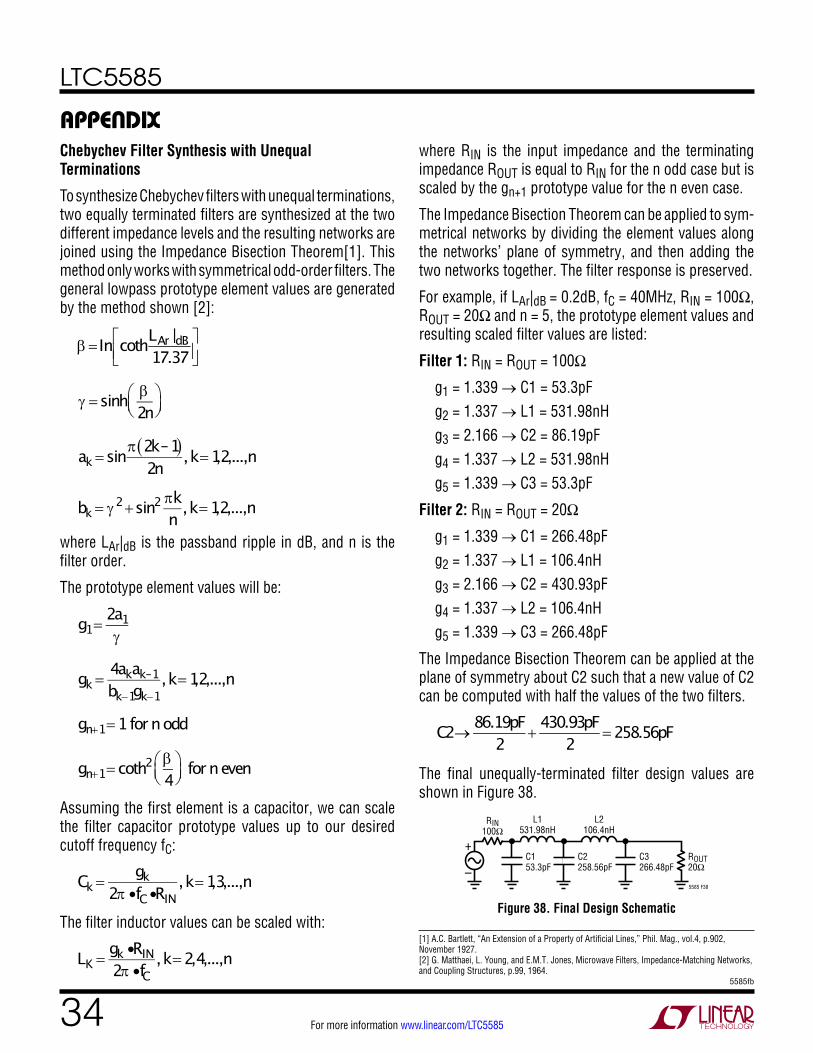
LTC5585
345585fb
For more information www.linear.com/LTC5585
APPENDIXChebychev Filter Synthesis with Unequal Terminations
To synthesize Chebychev filters with unequal terminations, two equally terminated filters are synthesized at the two different impedance levels and the resulting networks are joined using the Impedance Bisection Theorem[1]. This method only works with symmetrical odd-order filters. The general lowpass prototype element values are generated by the method shown [2]:
β = In cothLAr |dB17.37
γ = sinh β2n
ak = sinπ 2k–1( )2n
,k=1,2,...,n
bk = γ 2+sin2 πkn
,k=1,2,...,n
where LAr|dB is the passband ripple in dB, and n is the filter order.
The prototype element values will be:
g1=2a1γ
gk =4akak–1bk−1gk−1
,k=1,2,...,n
gn+1=1 for n odd
gn+1= coth2 β4
for n even
Assuming the first element is a capacitor, we can scale the filter capacitor prototype values up to our desired cutoff frequency fC:
Ck =
gk2π •fC•RIN
,k=1,3,...,n
The filter inductor values can be scaled with:
LK =
gk •RIN2π •fC
,k= 2,4,...,n
where RIN is the input impedance and the terminating impedance ROUT is equal to RIN for the n odd case but is scaled by the gn+1 prototype value for the n even case.
The Impedance Bisection Theorem can be applied to sym-metrical networks by dividing the element values along the networks’ plane of symmetry, and then adding the two networks together. The filter response is preserved.
For example, if LAr|dB = 0.2dB, fC = 40MHz, RIN = 100Ω, ROUT = 20Ω and n = 5, the prototype element values and resulting scaled filter values are listed:
Filter 1: RIN = ROUT = 100Ω
g1 = 1.339 → C1 = 53.3pF g2 = 1.337 → L1 = 531.98nH g3 = 2.166 → C2 = 86.19pF g4 = 1.337 → L2 = 531.98nH g5 = 1.339 → C3 = 53.3pF
Filter 2: RIN = ROUT = 20Ω
g1 = 1.339 → C1 = 266.48pF g2 = 1.337 → L1 = 106.4nH g3 = 2.166 → C2 = 430.93pF g4 = 1.337 → L2 = 106.4nH g5 = 1.339 → C3 = 266.48pF
The Impedance Bisection Theorem can be applied at the plane of symmetry about C2 such that a new value of C2 can be computed with half the values of the two filters.
C2→
86.19pF2
+430.93pF
2= 258.56pF
The final unequally-terminated filter design values are shown in Figure 38.
Figure 38. Final Design Schematic
+
–
RIN100Ω
L1531.98nH
C153.3pF
C2258.56pF
L2106.4nH
C3266.48pF
ROUT20Ω
5585 F38
[1] A.C. Bartlett, “An Extension of a Property of Artificial Lines,” Phil. Mag., vol.4, p.902, November 1927. [2] G. Matthaei, L. Young, and E.M.T. Jones, Microwave Filters, Impedance-Matching Networks, and Coupling Structures, p.99, 1964.
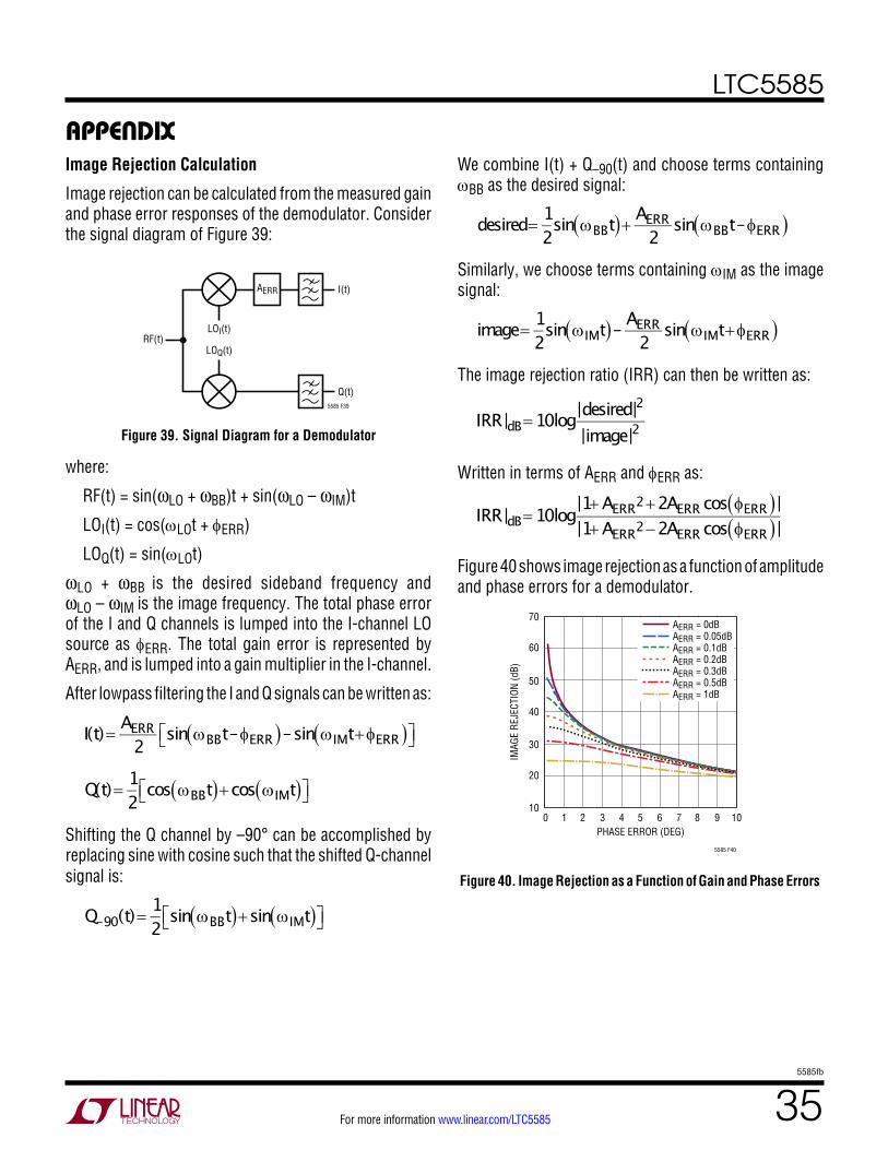
LTC5585
355585fb
For more information www.linear.com/LTC5585
APPENDIXImage Rejection Calculation
Image rejection can be calculated from the measured gain and phase error responses of the demodulator. Consider the signal diagram of Figure 39:
We combine I(t) + Q–90(t) and choose terms containing ωBB as the desired signal:
desired=
12
sin ωBBt( )+AERR
2sin ωBBt–φERR( )
Similarly, we choose terms containing ωIM as the image signal:
image=
12
sin ωIMt( )– AERR2
sin ωIMt+φERR( )
The image rejection ratio (IRR) can then be written as:
IRR|dB=10log|desired|2
|image|2
Written in terms of AERR and φERR as:
IRR|dB=10log|1+ AERR2+2AERR cos φERR( )|
|1+ AERR2−2AERR cos φERR( )|
Figure 40 shows image rejection as a function of amplitude and phase errors for a demodulator.
AERR
LOI(t)
LOQ(t)RF(t)
I(t)
Q(t)5585 F39
Figure 39. Signal Diagram for a Demodulator
where:
RF(t) = sin(ωLO + ωBB)t + sin(ωLO – ωIM)t
LOI(t) = cos(ωLOt + φERR)
LOQ(t) = sin(ωLOt)
ωLO + ωBB is the desired sideband frequency and ωLO – ωIM is the image frequency. The total phase error of the I and Q channels is lumped into the I-channel LO source as φERR. The total gain error is represented by AERR, and is lumped into a gain multiplier in the I-channel.
After lowpass filtering the I and Q signals can be written as:
I(t)=AERR
2sin ωBBt–φERR( )–sin ωIMt+φERR( )
Q(t)=12
cos ωBBt( )+cos ωIMt( )
Shifting the Q channel by –90° can be accomplished by replacing sine with cosine such that the shifted Q-channel signal is:
Q–90(t)=
12
sin ωBBt( )+sin ωIMt( )
Figure 40. Image Rejection as a Function of Gain and Phase Errors
PHASE ERROR (DEG)
10
IMAG
E RE
JECT
ION
(dB)
30
50
70
20
40
60
2 4 6 8
5585 F40
1010 3 5 7 9
AERR = 0dBAERR = 0.05dBAERR = 0.1dBAERR = 0.2dBAERR = 0.3dBAERR = 0.5dBAERR = 1dB
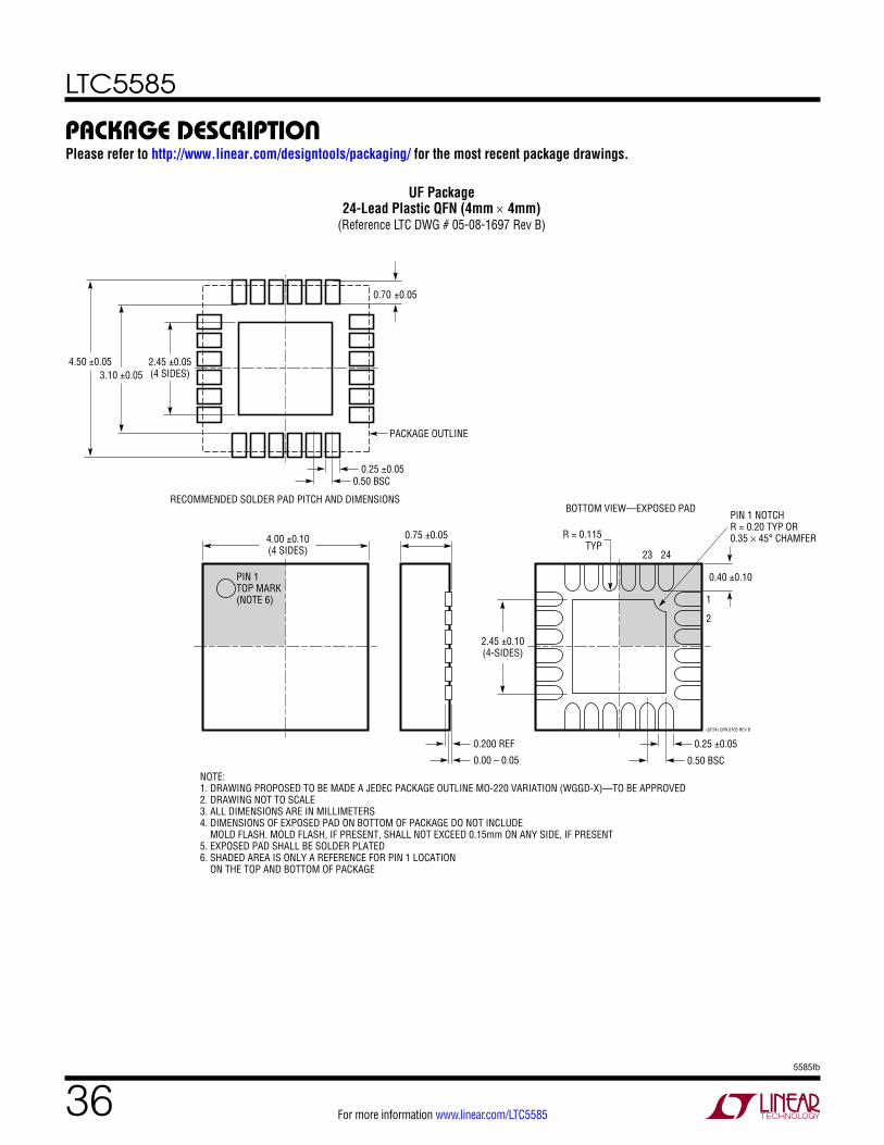
LTC5585
365585fb
For more information www.linear.com/LTC5585
PACKAGE DESCRIPTIONPlease refer to http://www.linear.com/designtools/packaging/ for the most recent package drawings.
UF Package24-Lead Plastic QFN (4mm × 4mm)
(Reference LTC DWG # 05-08-1697 Rev B)
4.00 ±0.10(4 SIDES)
NOTE:1. DRAWING PROPOSED TO BE MADE A JEDEC PACKAGE OUTLINE MO-220 VARIATION (WGGD-X)—TO BE APPROVED2. DRAWING NOT TO SCALE3. ALL DIMENSIONS ARE IN MILLIMETERS4. DIMENSIONS OF EXPOSED PAD ON BOTTOM OF PACKAGE DO NOT INCLUDE MOLD FLASH. MOLD FLASH, IF PRESENT, SHALL NOT EXCEED 0.15mm ON ANY SIDE, IF PRESENT5. EXPOSED PAD SHALL BE SOLDER PLATED6. SHADED AREA IS ONLY A REFERENCE FOR PIN 1 LOCATION ON THE TOP AND BOTTOM OF PACKAGE
PIN 1TOP MARK(NOTE 6)
0.40 ±0.10
2423
1
2
BOTTOM VIEW—EXPOSED PAD
2.45 ±0.10(4-SIDES)
0.75 ±0.05 R = 0.115TYP
0.25 ±0.05
0.50 BSC
0.200 REF
0.00 – 0.05
(UF24) QFN 0105 REV B
RECOMMENDED SOLDER PAD PITCH AND DIMENSIONS
0.70 ±0.05
0.25 ±0.050.50 BSC
2.45 ±0.05(4 SIDES)3.10 ±0.05
4.50 ±0.05
PACKAGE OUTLINE
PIN 1 NOTCHR = 0.20 TYP OR 0.35 × 45° CHAMFER
UF Package24-Lead Plastic QFN (4mm × 4mm)
(Reference LTC DWG # 05-08-1697 Rev B)
LTC5585
375585fb
For more information www.linear.com/LTC5585
Information furnished by Linear Technology Corporation is believed to be accurate and reliable. However, no responsibility is assumed for its use. Linear Technology Corporation makes no representa-tion that the interconnection of its circuits as described herein will not infringe on existing patent rights.
REVISION HISTORYREV DATE DESCRIPTION PAGE NUMBER
A 8/12 Changes to 1950MHz L6, C19 and L5 Matching Component ValuesCorrection to Plot 5585 G4 Vertical Axis LabelChanges to Plot G20Changes to Plots G30 and G35 Corrections to Plot G44 Horizontal Axis LabelChanges to Plot G61Changes to Plot G78Changes to Figure 1, RF and LO MATCH Table 1950MHz L6, C19 and L5 Component ValuesChanges to Figure 5, 1.9GHz L6 and C19 Component ValuesChange to Figure 13, 1.9GHz L5 Component ValueAdded Reduced Power Consumption Paragraph TitleCorrection to Figure 32 TitleCorrection to text 1875Hz
368
10111315182022292931
B 11/14 Changes to Features and DescriptionChange to 700MHz IRRInsert 3500MHz Data and Supply Current ConditionCorrection to Plot G19 Vertical Axis LabelCorrection to Plot G34 Vertical Axis LabelCorrection to Plot G45 Horizontal Axis LabelCorrection to Plot G60 Vertical Axis LabelCorrection to Plot G77 Vertical Axis LabelChange to Figure 1 RF MATCH 2150MHz Table ValuesChange to Figure 13 C13 and L5 Component ValuesChange to text "lag (or lead)"Omission of 6mA Current ArrowsChange in Figure 22 C ValueChange in Figure 33 ADC Output D15Change in Typical Application ADC Output D15
1348
1011131518222324263038
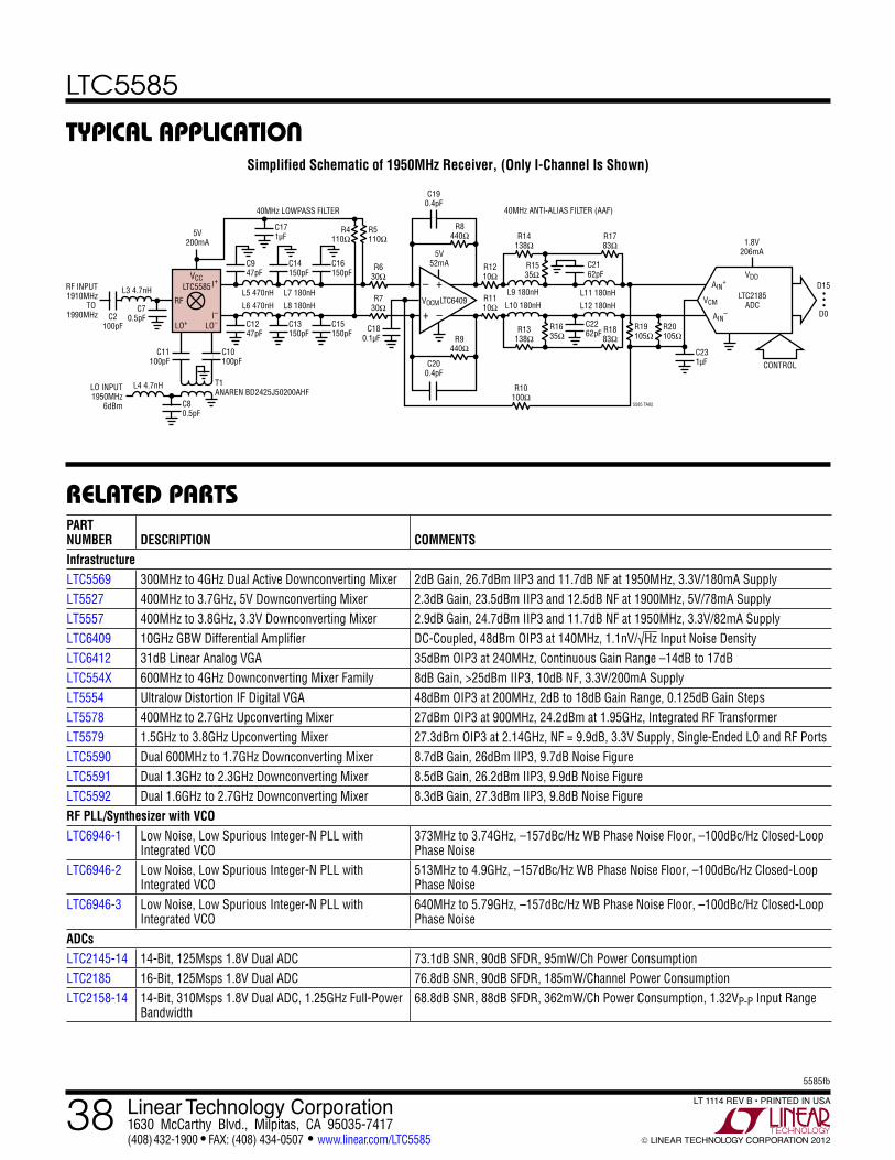
LTC5585
385585fb
For more information www.linear.com/LTC5585 LINEAR TECHNOLOGY CORPORATION 2012
LT 1114 REV B • PRINTED IN USALinear Technology Corporation1630 McCarthy Blvd., Milpitas, CA 95035-7417(408) 432-1900 FAX: (408) 434-0507 www.linear.com/LTC5585
RELATED PARTS
TYPICAL APPLICATIONSimplified Schematic of 1950MHz Receiver, (Only I-Channel Is Shown)
D15
D0
CONTROL
VCM
VDD
LTC2185ADC
1.8V206mA
5V200mA
AIN+
AIN–
R20105Ω
C2262pF
C2162pF
R19105Ω
R1635Ω
R1535Ω
R5110Ω
R4110Ω
C231µF
5585 TA02
R1883Ω
R1783Ω
R10100Ω
R1210Ω
R8440Ω
R9440Ω
R730Ω
R630Ω
R1110Ω
R13138Ω
R14138Ω
5V52mA
C190.4pF
C200.4pF
C180.1µF
L12 180nH
L11 180nH
L8 180nH
L7 180nH
40MHz LOWPASS FILTER
L6 470nH
L3 4.7nH
L4 4.7nH T1ANAREN BD2425J50200AHF
L5 470nHL10 180nH
L9 180nH •••
C15150pF
C16150pF
C171µF
–
–+
+VOCMLTC6409
C13150pF
C14150pF
C1247pF
C10100pF
C11100pF
LO INPUT1950MHz
6dBm
C947pF
C70.5pFC2
100pF
C80.5pF
I+VCC
I–RF
LO–LO+
LTC5585RF INPUT1910MHz
TO 1990MHz
40MHz ANTI-ALIAS FILTER (AAF)
PART NUMBER DESCRIPTION COMMENTSInfrastructureLTC5569 300MHz to 4GHz Dual Active Downconverting Mixer 2dB Gain, 26.7dBm IIP3 and 11.7dB NF at 1950MHz, 3.3V/180mA SupplyLT5527 400MHz to 3.7GHz, 5V Downconverting Mixer 2.3dB Gain, 23.5dBm IIP3 and 12.5dB NF at 1900MHz, 5V/78mA SupplyLT5557 400MHz to 3.8GHz, 3.3V Downconverting Mixer 2.9dB Gain, 24.7dBm IIP3 and 11.7dB NF at 1950MHz, 3.3V/82mA SupplyLTC6409 10GHz GBW Differential Amplifier DC-Coupled, 48dBm OIP3 at 140MHz, 1.1nV/√Hz Input Noise DensityLTC6412 31dB Linear Analog VGA 35dBm OIP3 at 240MHz, Continuous Gain Range –14dB to 17dBLTC554X 600MHz to 4GHz Downconverting Mixer Family 8dB Gain, >25dBm IIP3, 10dB NF, 3.3V/200mA SupplyLT5554 Ultralow Distortion IF Digital VGA 48dBm OIP3 at 200MHz, 2dB to 18dB Gain Range, 0.125dB Gain StepsLT5578 400MHz to 2.7GHz Upconverting Mixer 27dBm OIP3 at 900MHz, 24.2dBm at 1.95GHz, Integrated RF TransformerLT5579 1.5GHz to 3.8GHz Upconverting Mixer 27.3dBm OIP3 at 2.14GHz, NF = 9.9dB, 3.3V Supply, Single-Ended LO and RF PortsLTC5590 Dual 600MHz to 1.7GHz Downconverting Mixer 8.7dB Gain, 26dBm IIP3, 9.7dB Noise FigureLTC5591 Dual 1.3GHz to 2.3GHz Downconverting Mixer 8.5dB Gain, 26.2dBm IIP3, 9.9dB Noise FigureLTC5592 Dual 1.6GHz to 2.7GHz Downconverting Mixer 8.3dB Gain, 27.3dBm IIP3, 9.8dB Noise FigureRF PLL/Synthesizer with VCOLTC6946-1 Low Noise, Low Spurious Integer-N PLL with
Integrated VCO373MHz to 3.74GHz, –157dBc/Hz WB Phase Noise Floor, –100dBc/Hz Closed-Loop Phase Noise
LTC6946-2 Low Noise, Low Spurious Integer-N PLL with Integrated VCO
513MHz to 4.9GHz, –157dBc/Hz WB Phase Noise Floor, –100dBc/Hz Closed-Loop Phase Noise
LTC6946-3 Low Noise, Low Spurious Integer-N PLL with Integrated VCO
640MHz to 5.79GHz, –157dBc/Hz WB Phase Noise Floor, –100dBc/Hz Closed-Loop Phase Noise
ADCsLTC2145-14 14-Bit, 125Msps 1.8V Dual ADC 73.1dB SNR, 90dB SFDR, 95mW/Ch Power ConsumptionLTC2185 16-Bit, 125Msps 1.8V Dual ADC 76.8dB SNR, 90dB SFDR, 185mW/Channel Power ConsumptionLTC2158-14 14-Bit, 310Msps 1.8V Dual ADC, 1.25GHz Full-Power
Bandwidth68.8dB SNR, 88dB SFDR, 362mW/Ch Power Consumption, 1.32VP-P Input Range

![IIP2-improved Frontend Receiver using a Mismatch ... JAE-KYUNG LEE et al : IIP2-IMPROVED FRONTEND RECEIVER USING A MISMATCH COMPENSATION LNA using the current DAC [9]. Section II analyzes](https://img.pdfslide.net/doc/110x75/5b2f57587f8b9ac06e8d450e/iip2-improved-frontend-receiver-using-a-mismatch-jae-kyung-lee-et-al-iip2-improved.jpg)