Embed Size (px)
Citation preview
LTC7805
1Rev. 0
For more information www.analog.comDocument Feedback
TYPICAL APPLICATION
FEATURES DESCRIPTION
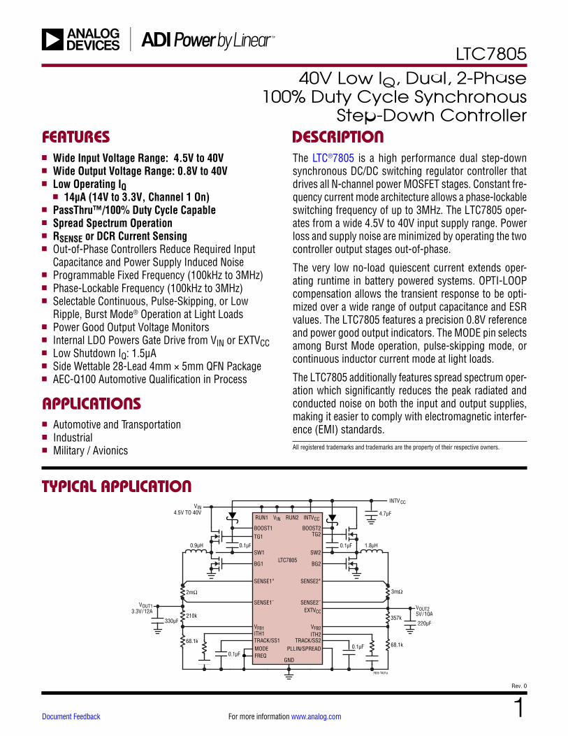
40V Low IQ, Dual, 2-Phase 100% Duty Cycle Synchronous
Step-Down Controller
The LTC®7805 is a high performance dual step-down synchronous DC/DC switching regulator controller that drives all N-channel power MOSFET stages. Constant fre-quency current mode architecture allows a phase-lockable switching frequency of up to 3MHz. The LTC7805 oper-ates from a wide 4.5V to 40V input supply range. Power loss and supply noise are minimized by operating the two controller output stages out-of-phase.
The very low no-load quiescent current extends oper-ating runtime in battery powered systems. OPTI-LOOP compensation allows the transient response to be opti-mized over a wide range of output capacitance and ESR values. The LTC7805 features a precision 0.8V reference and power good output indicators. The MODE pin selects among Burst Mode operation, pulse-skipping mode, or continuous inductor current mode at light loads.
The LTC7805 additionally features spread spectrum oper-ation which significantly reduces the peak radiated and conducted noise on both the input and output supplies, making it easier to comply with electromagnetic interfer-ence (EMI) standards.
APPLICATIONS
n Wide Input Voltage Range: 4.5V to 40V n Wide Output Voltage Range: 0.8V to 40V n Low Operating IQ
n 14μA (14V to 3.3V, Channel 1 On) n PassThru™/100% Duty Cycle Capable n Spread Spectrum Operation n RSENSE or DCR Current Sensing n Out-of-Phase Controllers Reduce Required Input
Capacitance and Power Supply Induced Noise n Programmable Fixed Frequency (100kHz to 3MHz) n Phase-Lockable Frequency (100kHz to 3MHz) n Selectable Continuous, Pulse-Skipping, or Low
Ripple, Burst Mode® Operation at Light Loads n Power Good Output Voltage Monitors n Internal LDO Powers Gate Drive from VIN or EXTVCC n Low Shutdown IQ: 1.5μA n Side Wettable 28-Lead 4mm × 5mm QFN Package n AEC-Q100 Automotive Qualification in Process
n Automotive and Transportation n Industrial n Military / Avionics All registered trademarks and trademarks are the property of their respective owners.
VOUT2VOUT1
VIN
0.1µF0.9µH
2mΩ
4.7µF
210k
68.1k
330µF
0.1µF
0.1µF 1.8µH
3mΩ
0.1µF
357k
68.1k
220µF
LTC7805SW1
BG1
TG1BOOST1
SENSE1+
SENSE1–
RUN1 VIN RUN2 INTVCC
INTV CC
EXTVCC
VFB1ITH1TRACK/SS1
GND
SW2
BG2
TG2BOOST2
SENSE2+
SENSE2–
VFB2ITH2
TRACK/SS2MODE PLLIN/SPREAD
3.3V/12A 5V/10A
4.5V TO 40V
FREQ
7805 TA01a
LTC7805
2Rev. 0
For more information www.analog.com
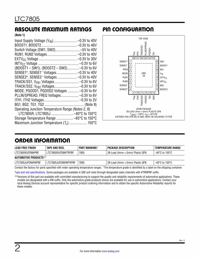
PIN CONFIGURATIONABSOLUTE MAXIMUM RATINGS
Input Supply Voltage (VIN) ......................... –0.3V to 40VBOOST1, BOOST2 ...................................... –0.3V to 46VSwitch Voltage (SW1, SW2) .......................... –5V to 40VRUN1, RUN2 Voltages ................................ –0.3V to 40VEXTVCC Voltage ......................................... –0.3V to 30VINTVCC Voltage ............................................ –0.3V to 6V(BOOST1 – SW1), (BOOST2 – SW2) ............ –0.3V to 6VSENSE1+, SENSE1– Voltages ...................... –0.3V to 40VSENSE2+, SENSE2– Voltages ..................... –0.3V to 40VTRACK/SS1, VFB1 Voltages .......................... –0.3V to 6VTRACK/SS2, VFB2 Voltages .......................... –0.3V to 6VMODE, PGOOD1, PGOOD2 Voltages ............ –0.3V to 6VPLLIN/SPREAD, FREQ Voltages ................... –0.3V to 6VITH1, ITH2 Voltages ..................................... –0.3V to 2VBG1, BG2, TG1, TG2 ........................................... (Note 9)Operating Junction Temperature Range (Notes 2, 8) LTC7805R, LTC7805J ........................ –40°C to 150°CStorage Temperature Range .................. –65°C to 150°CMaximum Junction Temperature (TJ) ................... 150°C
(Note 1)TOP VIEW
UFDM PACKAGE28-LEAD (4mm × 5mm) PLASTIC QFN
TJMAX = 150°C, θJA = 43°C/WEXPOSED PAD (PIN 29) IS GND, MUST BE SOLDERED TO PCB
6
5
4
3
2
1SENSE1+
SENSE1–
FREQ
MODE
RUN1
RUN2
SENSE2–
SENSE2+
SW1
BOOST1
BG1
VIN
EXTVCC
INTVCC
BG2
BOOST2
28 27 26
GND29
25 24 23
V FB1
ITH1
TRAC
K/SS
1
PLLI
N/SP
READ
PGOO
D1
TG1
7
17
18
19
20
21
22
16
8 159 10 11 12 13 14
V FB2
ITH2
TRAC
K/SS
2
PGOO
D2 TG2
SW2
ORDER INFORMATIONLEAD FREE FINISH TAPE AND REEL PART MARKING* PACKAGE DESCRIPTION TEMPERATURE RANGE
LTC7805RUFDM#PBF LTC7805RUFDM#TRPBF 7805 28-Lead (4mm × 5mm) Plastic QFN −40°C to 150°C
AUTOMOTIVE PRODUCTS**
LTC7805JUFDM#WPBF LTC7805JUFDM#WTRPBF 7805 28-Lead (4mm × 5mm) Plastic QFN −40°C to 150°C
Contact the factory for parts specified with wider operating temperature ranges. *The temperature grade is identified by a label on the shipping container.
Tape and reel specifications. Some packages are available in 500 unit reels through designated sales channels with #TRMPBF suffix.**Versions of this part are available with controlled manufacturing to support the quality and reliability requirements of automotive applications. These
models are designated with a #W suffix. Only the automotive grade products shown are available for use in automotive applications. Contact your local Analog Devices account representative for specific product ordering information and to obtain the specific Automotive Reliability reports for these models.

LTC7805
3Rev. 0
For more information www.analog.com
ELECTRICAL CHARACTERISTICS
SYMBOL PARAMETER CONDITIONS MIN TYP MAX UNITS
Input Supply (VIN)
VIN Input Supply Operating Range 4.5 40 V
IQ Total Input Supply Current in Regulation Front Page Circuit, 14V to 3.3V, No Load, RUN2 = 0V
14 µA
Controller Operation
VOUT1,2 Output Voltage Operating Range 0.8 40 V
VFB1,2 Regulated Feedback Voltage (Note 4) VIN = 4.5V to 40V, ITH1,2 Voltage = 0.6V to 1.2V 0°C to 85°C, All Grades
l
0.788 0.792
0.800 0.800
0.812 0.808
V V
Feedback Current ±5 ±50 nA
Feedback Overvoltage Protection Threshold Measured at VFB1,2 Relative to Regulated VFB1,2
7 10 13 %
gm1,2 Transconductance Amplifier gm (Note 4) ITH1,2 = 1.2V, Sink/Source = 5μA 1.8 mmho
VSENSE(MAX) Maximum Current Sense Threshold VFB1,2 = 0.7V, VSENSE1,2– = 3.3V l 43 50 55 mV
Matching Between Channels VSENSE1,2– = 3.3V –3.5 0 3.5 mV
ISENSE1,2+ SENSE1, 2+ Pin Current VSENSE1,2+ = 3V ±1 µA
ISENSE1– SENSE1– Pin Current VSENSE1– ≤ 2.8V 3.2V ≤ VSENSE1– < INTVCC – 0.5V VSENSE1– > INTVCC + 0.5V
2 50
750
µA µA µA
ISENSE2– SENSE2– Pin Current VSENSE2– = 3.3V VSENSE2– > INTVCC + 0.5V
700
±2 µA µA
Soft-Start Charge Current VTRACK/SS1,2 = 0V 10 12.5 15 µA
RUN Pin ON Threshold VRUN1,2 Rising l 1.15 1.20 1.25 V
RUN Pin Hysteresis 100 mV
DC Supply Current (Note 5)
VIN Shutdown Current RUN1,2 = 0V 1.5 µA
VIN Sleep Mode Current VSENSE1– < 3.2V, EXTVCC = 0V One Channel On Both Channels On
15 18
24 30
µA µA
Sleep Mode Current (Note 3) Only Channel 1 On
VSENSE1– ≥ 3.2V VIN Current, EXTVCC = 0V VIN Current, EXTVCC ≥ 4.8V EXTVCC Current, EXTVCC ≥ 4.8V SENSE1– Current
5 1 5
10
9 4
10 18
µA µA µA µA
Sleep Mode Current (Note 3) Both Channels On
VSENSE1– ≥ 3.2V, EXTVCC ≥ 4.8V VIN Current EXTVCC Current SENSE1– Current
1 7
12
4
12 22
µA µA µA
Pulse-Skipping or Forced Continuous Mode VIN or EXTVCC Current (Note 3)
One Channel On Both Channels On
2 3
mA mA
The l denotes the specifications which apply over the full operating temperature range, otherwise specifications are at TA = 25°C, VIN = 12V, RUN1, 2 > 1.25V, EXTVCC = 0V, unless otherwise noted. (Note 2)

LTC7805
4Rev. 0
For more information www.analog.com
ELECTRICAL CHARACTERISTICS The l denotes the specifications which apply over the full operating temperature range, otherwise specifications are at TA = 25°C, VIN = 12V, RUN1, 2 > 1.25V, EXTVCC = 0V, unless otherwise noted. (Note 2)
SYMBOL PARAMETER CONDITIONS MIN TYP MAX UNITS
Gate Drivers
TG or BG On-Resistance Pull-Up Pull-Down
1.2 0.6
Ω Ω
TG or BG Transition Time Rise Time Fall Time
(Note 6) CLOAD = 3300pF CLOAD = 3300pF
20 10
ns ns
TG Off to BG On Delay Synchronous Switch-On Delay Time
CLOAD = 3300pF Each Driver 15 ns
BG Off to TG On Delay Top Switch-On Delay Time
CLOAD = 3300pF Each Driver 15 ns
tON(MIN)1,2 TG Minimum On-Time (Note 7) 40 ns
Maximum Duty Factor for TG 100 %
BOOST Charge Pump Available Output Current
VBOOST = 16V, VSW = 12V, FREQ = 0V, Forced Continuous Mode
100 180 µA
INTVCC Low Dropout (LDO) Linear Regulator
INTVCC Regulation Point 5.2 5.4 5.6 V
INTVCC Load Regulation ICC = 0mA to 100mA, VIN ≥ 6V ICC = 0mA to 100mA, VEXTVCC ≥ 6V
1.5 1.2
3 2
% %
EXTVCC LDO Switchover Voltage EXTVCC Rising 4.5 4.7 4.8 V
EXTVCC Switchover Hysteresis 250 mV
UVLO Undervoltage Lockout INTVCC Rising INTVCC Falling
l
l
4.10 3.75
4.20 3.90
4.40 4.00
V V
Spread Spectrum Oscillator and Phase-Locked Loop
fOSC Low Fixed Frequency VFREQ = 0V, PLLIN/SPREAD = 0V 320 370 420 kHz
High Fixed Frequency VFREQ = INTVCC, PLLIN/SPREAD = 0V l 2.0 2.25 2.5 MHz
Programmable Frequency RFREQ = 374kΩ, PLLIN/SPREAD = 0V RFREQ = 75kΩ, PLLIN/SPREAD = 0V RFREQ = 12.1kΩ, PLLIN/SPREAD = 0V
450
100 500 3
550
kHz kHz
MHz
Synchronizable Frequency Range PLLIN/SPREAD = External Clock l 0.1 3 MHz
PLLIN Input High Level PLLIN Input Low Level
l
l
2.2 0.5
V V
Spread Spectrum Frequency Range (Relative to fOSC)
PLLIN/SPREAD = INTVCC Minimum Frequency Maximum Frequency
0
20
% %
PGOOD1 and PGOOD2 Outputs
PGOOD Voltage Low IPGOOD1,2 = 2mA 0.2 0.4 V
PGOOD Leakage Current VPGOOD1,2 = 5V ±1 µA
PGOOD Trip Level VFB Relative to Set Regulation Point
VFB Rising Hysteresis
7 10 2.5
13 % %
VFB Falling Hysteresis
–13 –10 2.5
–7 % %
PGOOD Delay for Reporting a Fault 25 µs
LTC7805
5Rev. 0
For more information www.analog.com
ELECTRICAL CHARACTERISTICSNote 1: Stresses beyond those listed under Absolute Maximum Ratings may cause permanent damage to the device. Exposure to any Absolute Maximum Rating condition for extended periods may affect device reliability and lifetime.Note 2: The LTC7805R is specified over the –40°C to 150°C operating junction temperature range, and the LTC7805J is guaranteed over the –40°C to 150°C operating junction temperature range. High junction temperatures degrade operating lifetimes. Note that the maximum ambient temperature consistent with these specifications is determined by specific operating conditions in conjunction with board layout, the rated package thermal impedance and other environmental factors. The junction temperature (TJ, in °C) is calculated from the ambient temperature (TA, in °C) and power dissipation (PD, in Watts) according to the formula: TJ = TA + (PD • θJA), where θJA (in °C/W) is the package thermal impedance.Note 3: When SENSE1– ≥ 3.2V or EXTVCC ≥ 4.8V, VIN supply current is transferred to these pins to reduce the total input supply quiescent current. SENSE1– bias current is reflected to the channel 1 input supply by the formula IVIN1 = ISENSE1– • VOUT1/(VIN1 • η), where η is the efficiency. EXTVCC bias current is similarly reflected to the input supply when biased by an output. To minimize input supply current, select channel 1 to be the lowest output voltage greater than 3.2V and connect EXTVCC to the lowest output voltage greater than 4.8V
Note 4: The LTC7805 is tested in a feedback loop that servos VITH1,2 to a specified voltage and measures the resultant VFB1,2. The specification at 85°C is not tested in production and is assured by design, characterization and correlation to production testing at other temperatures.Note 5: Dynamic supply current is higher due to the gate charge being delivered at the switching frequency. See Applications Information.Note 6: Rise and fall times are measured using 10% and 90% levels. Delay times are measured using 50% levels.Note 7: The minimum on-time condition is specified for an inductor peak-to-peak ripple current >40% of IL(MAX) (See Minimum On-Time Considerations in the Applications Information section).Note 8: This IC includes overtemperature protection that is intended to protect the device during momentary overload conditions. The maximum rated junction temperature will be exceeded when this protection is active. Continuous operation above the specified absolute maximum operating junction temperature may impair device reliability or permanently damage the device.Note 9: Do not apply a voltage or current source to these pins. They must be connected to capacitive loads only, otherwise permanent damage may occur.

LTC7805
6Rev. 0
For more information www.analog.com
TYPICAL PERFORMANCE CHARACTERISTICS
Efficiency and Power Loss vs Load Current Efficiency vs Load Current Efficiency vs Input Voltage
Load Step Burst Mode Operation
Load Step Pulse-Skipping Mode
Load Step Forced Continuous Mode
Inductor Current at Light Load Soft Start-UpRegulated Feedback Voltage vs Temperature
VIN = 12VVOUT = 5V
BURST EFFICIENCY
PULSE–SKIPPINGEFFICIENCY
FIGURE 9 CIRCUIT
FCM EFFICIENCY
BURSTLOSS
PULSE–SKIPPINGLOSS
FCM LOSS
OUTPUT CURRENT (A)0.0001 0.001 0.01 0.1 1 100
10
20
30
40
50
60
70
80
90
100
0.001
0.01
0.1
1
10
100
EFFI
CIEN
CY (%
)
POWER LOSS (W
)
vs Output Current
7805 G01
FIGURE 9 CIRCUITBURST MODE OPERATION
VOUT = 5V
VIN = 8VVIN = 16VVIN = 24V
OUTPUT CURRENT (A)0.0001 0.001 0.01 0.1 1 1050
55
60
65
70
75
80
85
90
95
100
EFFI
CIEN
CY (%
)
Efficiency vs Load Current
7805 G02
FIGURE 9 CIRCUITILOAD1,2 = 8A
VOUT1 = 3.3V
VOUT2 = 5V
INPUT VOLTAGE (V)0 5 10 15 20 25 30 35 40
86
88
90
92
94
96
98
100
EFFI
CIEN
CY (%
)
Efficiency vs Input Voltage
7805 G03
VIN = 12VVOUT = 5V300mA TO 8A LOAD STEPFIGURE 9 CIRCUIT
50µs/DIV7805 G04
VOUT500mV/DIV
INDUCTORCURRENT
5A/DIV
LOADCURRENT
5A/DIV
VIN = 12VVOUT = 5V300mA TO 8A LOAD STEPFIGURE 9 CIRCUIT
50µs/DIV7805 G05
VOUT500mV/DIV
INDUCTORCURRENT
5A/DIV
LOADCURRENT
5A/DIV
VIN = 12VVOUT = 5V300mA TO 8A LOAD STEPFIGURE 9 CIRCUIT
50µs/DIV7805 G06
VOUT500mV/DIV
INDUCTORCURRENT
5A/DIV
LOADCURRENT
5A/DIV
Inductor Current at Light Load
VIN = 12VVOUT = 5VNO LOADFIGURE 9 CIRCUIT
4µs/DIV7805 G07
FORCEDCONTINUOUS
MODE
Burst ModeOPERATION
2A/DIV
PULSESKIPPING
MODE
Soft Start–Up
RUN1,25V/DIV
VOUT1 1V/DIV
VOUT21V/DIV
VIN = 12VFORCED CONTINUOUS MODEFIGURE 9 CIRCUIT
1ms/DIV
VOLT
AGE
7805 G08
TEMPERATURE (°C)–55 –25 5 35 65 95 125 155
792
794
796
798
800
802
804
806
808
REGU
LATE
D FE
EDBA
CK V
OLTA
GE (m
V)
7805 G09

LTC7805
7Rev. 0
For more information www.analog.com
TYPICAL PERFORMANCE CHARACTERISTICS
Current Sense Threshold vs ITH Voltage
SENSE1,2– Input Current vs VSENSE Voltage
SENSE1,2+ Input Current vs VSENSE Voltage
Foldback Current LimitSENSE1,2– Input Current vs Temperature
SENSE1,2+ Input Current vs Temperature
Oscillator Frequency vs Temperature
BOOST Charge Pump Output Current vs Frequency
BOOST Charge Pump Output Current vs SW Voltage
PULSE–SKIPPINGBurst Mode OPERATIONFORCED CONTINUOUS
ITH VOLTAGE (V)0 0.2 0.4 0.6 0.8 1.0 1.2 1.4
–30
–20
–10
0
10
20
30
40
50
CURR
ENT
SENS
E TH
RESH
OLD
(mV)
vs ITH Voltage
7805 G10
MODE = INTVCC
SENSE2– CURRENT
SENSE1– CURRENT
SENSE VOLTAGE (V)0 5 10 15 20 25 30 35 40
0
100
200
300
400
500
600
700
800
900
1000
SENS
E CU
RREN
T (µ
A)
7805 G11
MODE = INTVCC
SENSE+ VOLTAGE (V)
0 5 10 15 20 25 30 35 40–1.0
–0.8
–0.6
–0.4
–0.2
0.0
0.2
0.4
0.6
0.8
1.0
SENS
E+ CUR
ENT
(µA)
7805 G12
FEEDBACK VOLTAGE (mV)0 100 200 300 400 500 600 700 800
0
10
20
30
40
50
60
70
MAX
IMUM
CUR
RENT
SEN
SE T
HRES
HOLD
(mV)
7805 G13
SENSE1,2– = INTVCC + 0.5V
SENSE1– = 3.3V
SENSE2– = INTVCC – 0.5V
MODE = INTVCC
TEMPERATURE (°C)–55 –25 5 35 65 95 125 155
–100
0
100
200
300
400
500
600
700
800
900
SENS
E– CUR
RENT
(µA)
7805 G14
MODE = INTVCC
SENSE+ = 12V
SENSE+ = 1V
SENSE+ = 0V
TEMPERATURE (°C)–55 –25 5 35 65 95 125 155
–1.0
–0.8
–0.6
–0.4
–0.2
0.0
0.2
0.4
0.6
0.8
1.0
SENS
E+ CUR
RENT
(µA)
7805 G15
RFREQ=374k (100kHz)RFREQ=75k (500kHz)RFREQ=12.1k (3MHz)FREQ=GND (370kHz)FREQ=INTVCC (2.25MHz)
TEMPERATURE (°C)–55 –35 5 35 65 95 125 155
–6
–4
–2
0
2
4
6
8
10
CHAN
GE IN
FRE
QUEN
CY (%
)
7805 G16
SW = 12VBOOST = 16V
FREQUENCY (kHz)0 500 1000 1500 2000 2500 3000
0
30
60
90
120
150
180
210
240
270
300
CHAR
GE P
UMP
CURR
ENT
(uA)
7805 G17
TA = –55°CTA = 25°CTA = 150°C
DUTY CYCLE = 100%FREQ = 0V
TA = –55°CTA = 25°CTA = 150°C
SW VOLTAGE (V)0 5 10 15 20 25 30 35 40
0
50
100
150
200
250
CHAR
GE P
UMP
CURR
ENT
(µA)
7805 G18
LTC7805
8Rev. 0
For more information www.analog.com
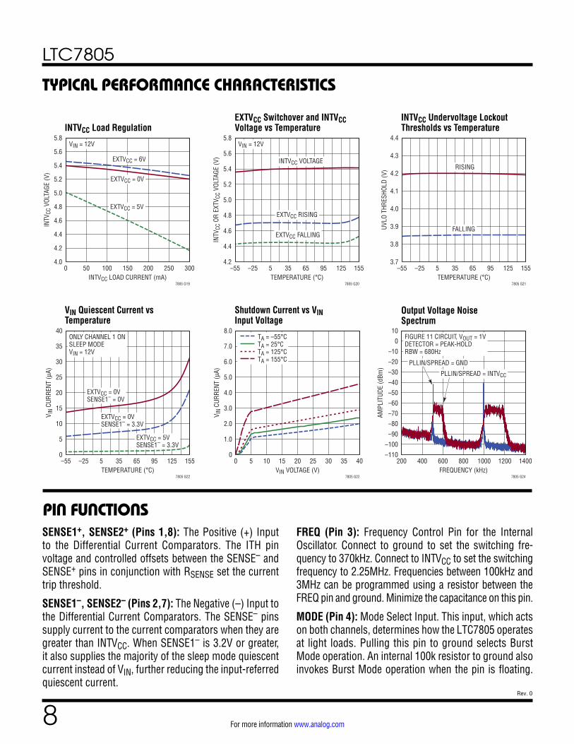
PIN FUNCTIONSSENSE1+, SENSE2+ (Pins 1,8): The Positive (+) Input to the Differential Current Comparators. The ITH pin voltage and controlled offsets between the SENSE– and SENSE+ pins in conjunction with RSENSE set the current trip threshold.
SENSE1–, SENSE2– (Pins 2,7): The Negative (–) Input to the Differential Current Comparators. The SENSE– pins supply current to the current comparators when they are greater than INTVCC. When SENSE1– is 3.2V or greater, it also supplies the majority of the sleep mode quiescent current instead of VIN, further reducing the input-referred quiescent current.
TYPICAL PERFORMANCE CHARACTERISTICS
FREQ (Pin 3): Frequency Control Pin for the Internal Oscillator. Connect to ground to set the switching fre-quency to 370kHz. Connect to INTVCC to set the switching frequency to 2.25MHz. Frequencies between 100kHz and 3MHz can be programmed using a resistor between the FREQ pin and ground. Minimize the capacitance on this pin.
MODE (Pin 4): Mode Select Input. This input, which acts on both channels, determines how the LTC7805 operates at light loads. Pulling this pin to ground selects Burst Mode operation. An internal 100k resistor to ground also invokes Burst Mode operation when the pin is floating.
INTVCC Load RegulationEXTVCC Switchover and INTVCC Voltage vs Temperature
INTVCC Undervoltage Lockout Thresholds vs Temperature
VIN Quiescent Current vs Temperature
Shutdown Current vs VIN Input Voltage
Output Voltage Noise Spectrum
EXTVCC = 5V
EXTVCC = 6V
EXTVCC = 0V
VIN = 12V
INTVCC LOAD CURRENT (mA)0 50 100 150 200 250 300
4.0
4.2
4.4
4.6
4.8
5.0
5.2
5.4
5.6
5.8
INTV
CC V
OLTA
GE (V
)
7805 G19
INTVCC VOLTAGE
EXTVCC RISING
EXTVCC FALLING
VIN = 12V
TEMPERATURE (°C)–55 –25 5 35 65 95 125 155
4.2
4.4
4.6
4.8
5.0
5.2
5.4
5.6
5.8
INTV
CC O
R EX
TVCC
VOL
TAGE
(V)
7805 G20
RISING
FALLING
TEMPERATURE (°C)–55 –25 5 35 65 95 125 155
3.7
3.8
3.9
4.0
4.1
4.2
4.3
4.4
UVLO
THR
ESHO
LD (V
)
7805 G21
ONLY CHANNEL 1 ONSLEEP MODEVIN = 12V
EXTVCC = 5VSENSE1– = 3.3V
EXTVCC = 0VSENSE1– = 3.3V
EXTVCC = 0VSENSE1– = 0V
TEMPERATURE (°C)–55 –25 5 35 65 95 125 155
0
5
10
15
20
25
30
35
40
V IN
CURR
ENT
(μA)
7805 G22VIN VOLTAGE (V)
0 5 10 15 20 25 30 35 400
1.0
2.0
3.0
4.0
5.0
6.0
7.0
8.0
V IN
CURR
ENT
(µA)
7805 G23
TA = –55°CTA = 25°CTA = 125°CTA = 155°C
FIGURE 11 CIRCUIT, VOUT = 1VDETECTOR = PEAK-HOLDRBW = 680Hz
PLLIN/SPREAD = GND
PLLIN/SPREAD = INTVCC
FREQUENCY (kHz)200 400 600 800 1000 1200 1400
–110
–100
–90
–80
–70
–60
–50
–40
–30
–20
–10
0
10
AMPL
ITUD
E (d
Bm)
7805 G24

LTC7805
9Rev. 0
For more information www.analog.com
PIN FUNCTIONSINTVCC pins and the BOOST2 and INTVCC pins. Voltage swing at the BOOST pins is from INTVCC to (VIN + INTVCC).
SW1, SW2 (Pins 22,14): Switch Node Connections to Inductors.
TG1, TG2 (Pins 23,13): High Current Gate Drives for Top N Channel MOSFETs. These are the outputs of floating drivers with a voltage swing of INTVCC superimposed on the switch node voltage SW.
PGOOD1, PGOOD2 (Pins 24,12): Open-Drain Power Good Outputs. The VFB1,2 pins are monitored to ensure that VOUT1,2 are in regulation. When VOUT is not within ±10% of its regulation point, the corresponding PGOOD pin is pulled low.
TRACK/SS1, TRACK/SS2 (Pins 26,11): External Tracking and Soft-Start Input. The LTC7805 regulates the VFB1,2 voltage to the lesser of 0.8V or the voltage on the TRACK/SS1,2 pin. Internal 12.5µA pull-up current sources are connected to these pins. A capacitor to ground sets the start-up ramp time to the final regulated output voltage. The ramp time is equal to 0.65ms for every 10nF of capac-itance. Alternatively, a resistor divider on another volt-age supply connected to the TRACK/SS pins allows the LTC7805 output to track the other supply during start-up.
ITH1, ITH2 (Pins 27,10): Error Amplifier Outputs and Switching Regulator Compensation Points. Each associ-ated channel’s current comparator trip point increases with this control voltage. Place compensation compo-nents between the ITH pins and ground.
VFB1, VFB2 (Pins 28,9): Controller Feedback Inputs. Connect an external resistor divider between the output voltage and the VFB pin to set the regulated output voltage. Tie VFB2 to INTVCC to configure the channels for a 2-phase single output application, in which both channels share VFB1, ITH1, and TRACK/SS1.
GND (Exposed Pad Pin 29): Ground. Connects to the sources of the bottom N-Channel MOSFETs and the (–) terminal(s) of decoupling capacitors. The exposed pad must be soldered to PCB ground for rated electrical and thermal performance.
Tying this pin to INTVCC forces continuous inductor cur-rent operation. Tying this pin to INTVCC through a 100k resistor selects pulse-skipping operation.
RUN1, RUN2 (Pins 5,6): Run Control Inputs for Each Controller. Forcing either of these pins below 1.1V disables switching of the corresponding controller. Forcing both of these pins below 0.7V shuts down the entire LTC7805, reducing quiescent current to approximately 1.5µA. These pins can be tied to VIN for always-on operation. Do not float the RUN pins.
INTVCC (Pin 17): Output of the Internal 5.4V Low Dropout Regulator. The driver and control circuits are powered by this supply. Must be decoupled to ground with a minimum of 4.7μF ceramic or tantalum capacitor.
EXTVCC (Pin 18): External Power Input to an Internal LDO Connected to INTVCC. This LDO supplies INTVCC power, bypassing the internal LDO powered from VIN whenever EXTVCC is higher than 4.7V. See INTVCC Regulators in the Applications Information section. Do not exceed 30V on this pin. Connect this pin to ground if the EXTVCC LDO is not used.
VIN (Pin 19): Main Bias Input Supply Pin. A bypass capac-itor should be tied between this pin and GND.
PLLIN/SPREAD (Pin 25): External Synchronization Input and Spread Spectrum Selection. When an external clock is applied to this pin, the phase-locked loop will force the rising TG1 signal to be synchronized with the rising edge of the external clock. When an external clock is present, the regulators operate in pulse-skipping mode if it is selected by the MODE pin, or in forced continuous mode otherwise. When not synchronizing to an external clock, tie this input to INTVCC to enable spread spectrum dithering of the oscil-lator or to ground to disable spread spectrum.
BG1, BG2 (Pins 20,16): High Current Gate Drives for Bottom (Synchronous) N-Channel MOSFETs. Voltage swing at these pins is from ground to INTVCC.
BOOST1, BOOST2 (Pins 21,15): Bootstrapped Supplies to the Top Side Floating Drivers. Connect capacitors between the corresponding BOOST and SW pins for each channel. Also connect Schottky diodes between the BOOST1 and

LTC7805
10Rev. 0
For more information www.analog.com
FUNCTIONAL DIAGRAM
7805 BD
SWITCHLOGIC
INTVCC
VIN
VOUT1,2
DB
CB
BOOST
TG
SW
BG
PGND
SENSE–
SENSE+
CIN
INTVCC
L RSENSE
TOP
BOT
SPREADSPECTRUM
OSCILLATORAND PLL S
QR
SLEEP
+–+
–
+– +–
ICMP IR
5.4V5.4V
4.7VEN EN
EXTVCC LDO VIN LDO
1.4V
0.88V0V
0.72V
ITHCLAMP
SLOPE COMP
VFB
ITH
2mV
0.8V–++
TRACK/SS
ALLOFF
PGOOD
12.5µACC2 CC1
RF2
RC
RF1
EA
RUN
PLLIN/SPREAD
MODE
VIN
EXTVCC
INTVCC
FREQCLK2
CLK1
DUPLICATE FOR SECOND CONTROLLER CHANNEL
ALLOFF
TOP ON
1.2V
–
+
–
+
–
+
0.425V
–
+
DROPOUTDETECT
COUT
CSS
100k
–
+
–
+
–
+
CHARGEPUMP

LTC7805
11Rev. 0
For more information www.analog.com
OPERATIONMain Control Loop
The LTC7805 is a dual synchronous step-down (buck) controller utilizing a constant frequency, peak current mode architecture. The two controller channels oper-ate 180° out of phase which reduces the required input capacitance and power supply induced noise. During nor-mal operation, the external top MOSFET is turned on when the clock for that channel sets the SR latch, causing the inductor current to increase. The main switch is turned off when the main current comparator, ICMP, resets the SR latch. After the top MOSFET is turned off each cycle, the bottom MOSFET is turned on which causes the inductor current to decrease until either the inductor current starts to reverse, as indicated by the current comparator IR, or the beginning of the next clock cycle.
The peak inductor current at which ICMP trips and resets the latch is controlled by the voltage on the ITH pin, which is the output of the error amplifier EA. The error amplifier compares the output voltage feedback signal at the VFB pin, (which is generated with an external resistor divider connected across the output voltage, VOUT, to ground) to the internal 0.8V reference voltage. When the load cur-rent increases, it causes a slight decrease in VFB relative to the reference,which causes the EA to increase the ITH voltage until the average inductor current matches the new load current.
Power and Bias Supplies (VIN, EXTVCC, and INTVCC)
The INTVCC pin supplies power for the top and bottom MOSFET drivers and most of the internal circuitry. LDOs (low dropout linear regulators) are available from both the VIN and EXTVCC pins to provide power to INTVCC, which has a regulation point of 5.4V. When the EXTVCC pin is left open or tied to a voltage less than 4.7V, the VIN LDO supplies power to INTVCC. If EXTVCC is taken above 4.7V (typical), the VIN LDO is turned off and the EXTVCC LDO is turned on. Once enabled, the EXTVCC LDO supplies power to INTVCC. Using the EXTVCC pin allows the INTVCC power to be derived from a high efficiency external source such as one of the LTC7805 switching regulator outputs.
Each top MOSFET driver is biased from the floating boot-strap capacitor CB, which normally recharges during each cycle through an external diode when the switch voltage goes low.
If the input voltage decreases to a voltage close to the regulation point, the bottom MOSFET on-time may be too short to recharge the bootstrap capacitor. The LTC7805 detects this and extends the bottom MOSFET on-time every tenth cycle to charge the bootstrap capacitor. If the input voltage drops below the regulation point, the top MOSFET turns on continuously and the bootstrap capaci-tor CB is charged by an internal charge pump.
Start-Up and Shutdown (RUN and TRACK/SS Pins)
The two channels of the LTC7805 can be independently shut down using the RUN1 and RUN2 pins. Pulling a RUN pin below 1.1V shuts down the main control loop for that channel. Pulling both RUN pins below 0.7V disables both controllers and most internal circuits, including the INTVCC LDOs. In this shutdown state, the LTC7805 draws only 1.5μA of quiescent current.
The RUN pins may be externally pulled up or driven directly by logic. Each pin can tolerate up to 40V (abso-lute maximum), so it can be conveniently tied to VIN in always-on applications where one or both controllers are enabled continuously and never shut down. Additionally, a resistive divider from VIN to a RUN pin can be used to set a precise input undervoltage lockout so that the power supply does not operate below a user adjustable level.
The start-up of each channel’s output voltage VOUT is con-trolled by the voltage on the corresponding TRACK/SS pin. When the voltage on the TRACK/SS pin is less than the 0.8V internal reference voltage, the LTC7805 regulates the VFB voltage to the TRACK/SS pin voltage instead of the 0.8V reference voltage. This allows the TRACK/SS pin to be used as a soft-start which smoothly ramps the output voltage on start-up, thereby limiting the input sup-ply inrush current. An external capacitor from the TRACK/SS pin to GND is charged by an internal 12.5μA pull-up current, creating a voltage ramp on the TRACK/SS pin. As the TRACK/SS voltage rises linearly from 0V to 0.8V (and
(Refer to Functional Diagram)

LTC7805
12Rev. 0
For more information www.analog.com
OPERATIONbeyond), the output voltage VOUT rises smoothly from zero to its final value.
Alternatively, the TRACK/SS pins can be used to make the start-up of VOUT track that of another supply. Typically this requires connecting to the TRACK/SS pin through an external resistor divider from the other supply to ground (see the Applications Information section).
Light Load Operation: Burst Mode Operation, Pulse-Skipping, or Forced Continuous Mode (MODE Pin)
The LTC7805 can be set to enter high efficiency Burst Mode operation, constant frequency pulse-skipping mode or forced continuous conduction mode at low load currents.
To select Burst Mode operation, tie the MODE pin to ground. To select forced continuous operation, tie the MODE pin to INTVCC. To select pulse-skipping mode, tie the MODE pin to a DC voltage greater than 1.2V and less than INTVCC – 1.3V. An internal 100k resistor to ground invokes Burst Mode operation when the MODE pin is floating and pulse-skipping mode when the MODE pin is tied to INTVCC through an external 100k resistor.
When the controllers are enabled for Burst Mode opera-tion, the minimum peak current in the inductor is set to approximately 25% of its maximum value even though the voltage on the ITH pin might indicate a lower value. If the average inductor current is higher than the load cur-rent, the error amplifier EA will decrease the voltage on the ITH pin. When the ITH voltage drops below 0.425V, the internal sleep signal goes high (enabling sleep mode) and both external MOSFETs are turned off. The ITH pin is then disconnected from the output of the EA and parked at 0.45V.
In sleep mode, much of the internal circuitry is turned off, reducing the quiescent current that the LTC7805 draws. If one channel is in sleep mode and the other channel is shut down, the LTC7805 draws only 15μA of quiescent current. If both channels are in sleep mode, the LTC7805 draws only 18μA of quiescent current. When VOUT on channel 1 is 3.2V or higher, the majority of this quiescent current is supplied by the SENSE1– pin, which further reduces the
input-referred quiescent current by the ratio of VIN/VOUT multiplied by the efficiency.
In sleep mode, the load current is supplied by the output capacitor. As the output voltage decreases, the EA’s out-put begins to rise. When the output voltage drops enough, the ITH pin is reconnected to the output of the EA, the sleep signal goes low, and the controller resumes normal operation by turning on the top MOSFET on the next cycle of the internal oscillator.
When a controller is enabled for Burst Mode operation, the inductor current is not allowed to reverse. The reverse current comparator (IR) turns off the bottom MOSFET just before the inductor current reaches zero, preventing it from reversing and going negative. Thus, the controller operates in discontinuous operation.
In forced continuous operation the inductor current is allowed to reverse at light loads or under large transient conditions. The peak inductor current is determined by the voltage on the ITH pin, just as in normal operation. In this mode, the efficiency at light loads is lower than in Burst Mode operation. However, continuous operation has the advantage of lower output voltage ripple and less interference to audio circuitry. In forced continuous mode, the output ripple is independent of load current.
When the MODE pin is connected for pulse-skipping mode, the LTC7805 operates in PWM pulse-skipping mode at light loads. In this mode, constant frequency operation is maintained down to approximately 1% of designed maximum output current. At very light loads, the current comparator ICMP may remain tripped for several cycles and force the top MOSFET to stay off for the same number of cycles (i.e., skipping pulses). The inductor cur-rent is not allowed to reverse (discontinuous operation). This mode, like forced continuous operation, exhibits low output ripple as well as low audio noise and reduced RF interference as compared to Burst Mode operation. It pro-vides higher low current efficiency than forced continuous mode, but not nearly as high as Burst Mode operation.
Unlike forced continuous mode and pulse-skipping mode, Burst Mode cannot be synchronized to an external clock. Therefore, if Burst Mode is selected and the switching

LTC7805
13Rev. 0
For more information www.analog.com
OPERATIONfrequency is synchronized to an external clock applied to the PLLIN/SPREAD pin, the LTC7805 switches from Burst Mode to forced continuous mode.
Frequency Selection, Spread Spectrum, and Phase-Locked Loop (FREQ and PLLIN/SPREAD Pins)
The free running switching frequency of the LTC7805 controllers is selected using the FREQ pin. Tying FREQ to GND selects 370kHz while tying FREQ to INTVCC selects 2.25MHz. Placing a resistor between FREQ and GND allows the frequency to be programmed between 100kHz and 3MHz.
Switching regulators can be particularly troublesome for applications where electromagnetic interference (EMI) is a concern. To improve EMI, the LTC7805 can oper-ate in spread spectrum mode, which is enabled by tying the PLLIN/SPREAD pin to INTVCC. This feature varies the switching frequency, 0% to 20% higher than the fre-quency set by the FREQ pin.
A phase-locked loop (PLL) is available on the LTC7805 to synchronize the internal oscillator to an external clock source connected to the PLLIN/SPREAD pin. The LTC7805’s PLL aligns the turn-on of controller 1’s exter-nal top MOSFET to the rising edge of the synchronizing signal. Thus, the turn-on of controller 2’s external top MOSFET is 180° out-of-phase to the rising edge of the external clock source.
The PLL frequency is prebiased to the free running fre-quency set by the FREQ pin before the external clock is applied. If prebiased near the external clock frequency, the PLL only needs to make slight changes in order to synchronize the rising edge of the external clock to the rising edge of TG1. For more rapid lock-in to the external clock, use the FREQ pin to set the internal oscillator to approximately the frequency of the external clock. The
LTC7805’s PLL is guaranteed to lock to an external clock source whose frequency is between 100kHz and 3MHz.
The PLLIN/SPREAD pin is TTL compatible with thresholds of 1.6V (rising) and 1.1V (falling) and is guaranteed to operate with a clock signal swing of 0.5V to 2.2V.
Output Overvoltage Protection
Each channel has an overvoltage comparator that guards against transient overshoots as well as other more seri-ous conditions that may overvoltage the output. When the VFB1,2 pin rises more than 10% above its regulation point of 0.8V, the top MOSFET is turned off and the bot-tom MOSFET is turned on until the overvoltage condition is cleared.
Foldback Current
When the output voltage falls to less than 50% of its nominal level, foldback current limiting is activated, pro-gressively lowering the peak current limit in proportion to the severity of the overcurrent or short-circuit condition. Foldback current limiting is disabled during the soft-start interval (as long as the VFB voltage is keeping up with the TRACK/SS1,2 voltage).
Power Good
Each channel has a PGOOD pin that is connected to an open drain of an internal N-channel MOSFET. The MOSFET turns on and pulls the PGOOD pin low when the VFB volt-age is not within ±10% of the 0.8V reference. The PGOOD pin is also pulled low when the RUN pin is low (shut down). When the VFB voltage is within the ±10% require-ment, the MOSFET is turned off and the pin is allowed to be pulled up by an external resistor to a source no greater than 6V, such as INTVCC.
LTC7805
14Rev. 0
For more information www.analog.com
The Typical Application on the first page is a basic LTC7805 application circuit. External component selection is largely driven by the load requirement and begins with the selection of the inductor, current sense components, operating frequency, and light load operating mode. The remaining power stage components, consisting of the input and output capacitors, and power MOSFETs can then be chosen. Next, feedback resistors are selected to set the desired output voltage. Then, the remaining external components are selected, such as for soft-start, biasing, and loop compensation.
Inductor Value Calculation
The operating frequency and inductor selection are inter-related in that higher operating frequencies allow the use of smaller inductor and capacitor values. So why would anyone ever choose to operate at lower frequencies with larger components? The answer is efficiency. A higher frequency generally results in lower efficiency because of MOSFET switching and gate charge losses. In addi-tion to this basic trade-off, the effect of inductor value on ripple current and low current operation must also be considered. The inductor value has a direct effect on ripple current.
The maximum average inductor current IL(MAX) is equal to the maximum output current. The peak current is equal to the average inductor current plus half of the inductor ripple current, ΔIL, which decreases with higher induc-tance or higher frequency and increases with higher VIN:
ΔIL =
1(f)(L)
VOUT 1−VOUTVIN
⎛
⎝⎜
⎞
⎠⎟
Accepting larger values of ΔIL allows the use of low induc-tances, but results in higher output voltage ripple and greater core losses. A reasonable starting point for setting ripple current is ΔIL = 0.3 • IL(MAX). The maximum ΔIL occurs at the maximum input voltage.
The inductor value also has secondary effects. The tran-sition to Burst Mode operation begins when the average inductor current required results in a peak current below 25% of the current limit determined by RSENSE. Lower
inductor values (higher ΔIL) will cause this to occur at lower load currents, which can cause a dip in efficiency in the upper range of low current operation.
Inductor Core Selection
Once the value for L is known, the type of inductor must be selected. High efficiency regulators generally can-not afford the core loss found in low cost powdered iron cores, forcing the use of more expensive ferrite or molypermalloy cores. Actual core loss is very dependent on inductance value selected. As inductance increases, core losses go down. Unfortunately, increased inductance requires more turns of wire and therefore copper losses will increase.
Ferrite designs have very low core loss and are preferred for high switching frequencies, so design goals can con-centrate on copper loss and preventing saturation. Ferrite core material saturates hard, which means that induc-tance collapses abruptly when the peak design current is exceeded. This results in an abrupt increase in inductor ripple current and consequent output voltage ripple. Do not allow the core to saturate!
Current Sense Selection
The LTC7805 can be configured to use either DCR (induc-tor resistance) sensing or low value resistor sensing. The choice between the two current sensing schemes is largely a design trade-off between cost, power con-sumption and accuracy. DCR sensing has become popular because it saves expensive current sensing resistors and is more power efficient, particularly in higher current and lower frequency applications. However, current sensing resistors provide the most accurate current limits for the controller. Other external component selection is driven by the load requirement and begins with the selection of RSENSE (if RSENSE is used) and inductor value.
The SENSE+ and SENSE– pins are the inputs to the cur-rent comparators. The common mode voltage range on these pins is 0V to 40V (absolute maximum), enabling the LTC7805 to regulate output voltages up to a maxi-mum of 40V. The SENSE+ pin is high impedance, drawing
APPLICATIONS INFORMATION
LTC7805
15Rev. 0
For more information www.analog.com
less than ≈1μA. This high impedance allows the current comparators to be used in inductor DCR sensing. The impedance of the SENSE– pin changes depending on the common mode voltage. When less than INTVCC – 0.5V, these pins are relatively high impedance, drawing ≈ 1μA. When above INTVCC + 0.5V, a higher current (≈700μA) flows into each pin. Between INTVCC – 0.5V and INTVCC + 0.5V, the current transitions from the smaller current to the higher current. Channel 1’s SENSE1– pin has an additional ≈50μA current when its voltage is above 3.2V to bias internal circuitry from VOUT1 instead of VIN, thereby reducing the input-referred supply current.
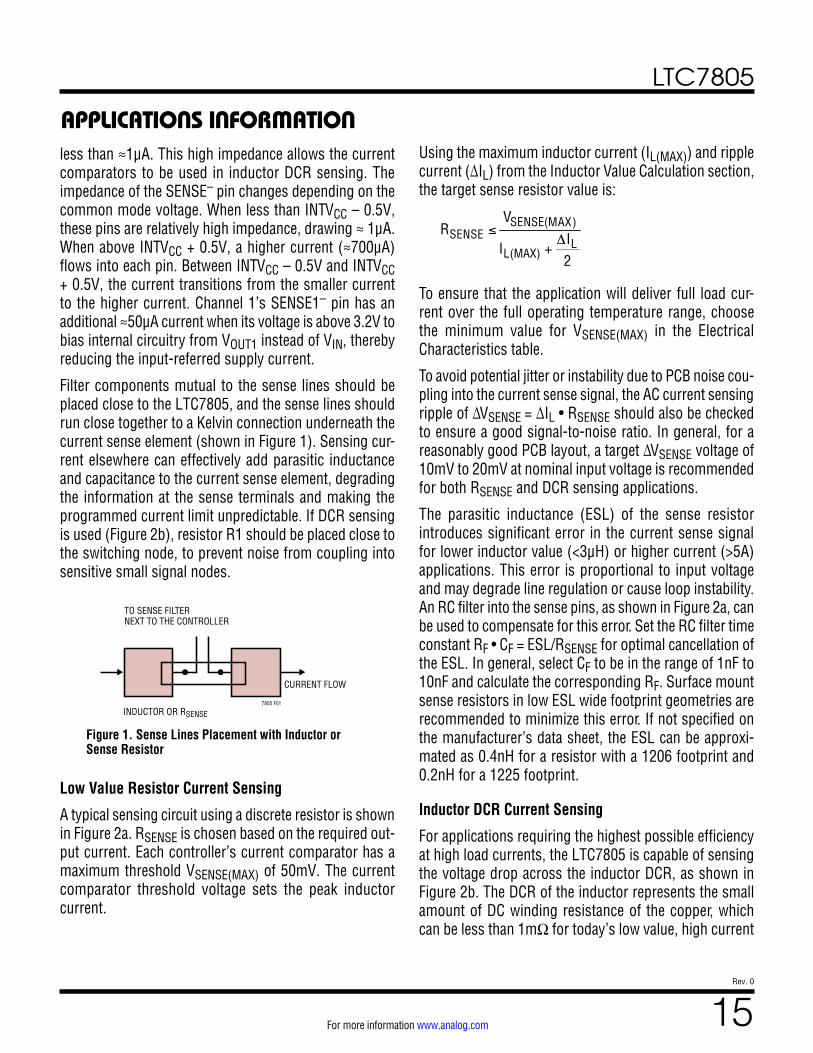
Filter components mutual to the sense lines should be placed close to the LTC7805, and the sense lines should run close together to a Kelvin connection underneath the current sense element (shown in Figure 1). Sensing cur-rent elsewhere can effectively add parasitic inductance and capacitance to the current sense element, degrading the information at the sense terminals and making the programmed current limit unpredictable. If DCR sensing is used (Figure 2b), resistor R1 should be placed close to the switching node, to prevent noise from coupling into sensitive small signal nodes.
Using the maximum inductor current (IL(MAX)) and ripple current (ΔIL) from the Inductor Value Calculation section, the target sense resistor value is:
RSENSE ≤VSENSE(MAX)
IL(MAX) +ΔIL2
To ensure that the application will deliver full load cur-rent over the full operating temperature range, choose the minimum value for VSENSE(MAX) in the Electrical Characteristics table.
To avoid potential jitter or instability due to PCB noise cou-pling into the current sense signal, the AC current sensing ripple of ΔVSENSE = ΔIL • RSENSE should also be checked to ensure a good signal-to-noise ratio. In general, for a reasonably good PCB layout, a target ΔVSENSE voltage of 10mV to 20mV at nominal input voltage is recommended for both RSENSE and DCR sensing applications.
The parasitic inductance (ESL) of the sense resistor introduces significant error in the current sense signal for lower inductor value (<3μH) or higher current (>5A) applications. This error is proportional to input voltage and may degrade line regulation or cause loop instability. An RC filter into the sense pins, as shown in Figure 2a, can be used to compensate for this error. Set the RC filter time constant RF • CF = ESL/RSENSE for optimal cancellation of the ESL. In general, select CF to be in the range of 1nF to 10nF and calculate the corresponding RF. Surface mount sense resistors in low ESL wide footprint geometries are recommended to minimize this error. If not specified on the manufacturer’s data sheet, the ESL can be approxi-mated as 0.4nH for a resistor with a 1206 footprint and 0.2nH for a 1225 footprint.
Inductor DCR Current Sensing
For applications requiring the highest possible efficiency at high load currents, the LTC7805 is capable of sensing the voltage drop across the inductor DCR, as shown in Figure 2b. The DCR of the inductor represents the small amount of DC winding resistance of the copper, which can be less than 1mΩ for today’s low value, high current
APPLICATIONS INFORMATION
Low Value Resistor Current Sensing
A typical sensing circuit using a discrete resistor is shown in Figure 2a. RSENSE is chosen based on the required out-put current. Each controller’s current comparator has a maximum threshold VSENSE(MAX) of 50mV. The current comparator threshold voltage sets the peak inductor current.
7805 F01
TO SENSE FILTERNEXT TO THE CONTROLLER
INDUCTOR OR RSENSE
CURRENT FLOW
Figure 1. Sense Lines Placement with Inductor or Sense Resistor

LTC7805
16Rev. 0
For more information www.analog.com
inductors. In a high current application requiring such an inductor, power loss through a sense resistor would cost several points of efficiency compared to inductor DCR sensing.
If the external (R1||R2) • C1 time constant is chosen to be exactly equal to the L/DCR time constant, the voltage drop across the external capacitor is equal to the drop across the inductor DCR multiplied by R2/(R1+R2). R2 scales the voltage across the sense terminals for applications where the DCR is greater than the target sense resistor value. To properly dimension the external filter components, the DCR of the inductor must be known. It can be measured using a good RLC meter, but the DCR tolerance is not always the same and varies with temperature; consult the manufacturers’ data sheets for detailed information.
Using the maximum inductor current (IL(MAX)) and ripple current (ΔIL) from the Inductor Value Calculation section, the target sense resistor value is:
RSENSE(EQUIV) =VSENSE(MAX)
ILMAX+ΔIL2
To ensure that the application will deliver full load cur-rent over the full operating temperature range, choose the minimum value for VSENSE(MAX) in the Electrical Characteristics table.
Next, determine the DCR of the inductor. When provided, use the manufacturer’s maximum value, usually given at 20°C. Increase this value to account for the temperature coefficient of copper resistance, which is approximately 0.4%/°C. A conservative value for TL(MAX) is 100°C. To scale the maximum inductor DCR to the desired sense resistor value, use the divider ratio:
RD =
RSENSE(EQUIV)DCRMAX atTL(MAX)
C1 is usually selected to be in the range of 0.1μF to 0.47μF. This forces R1||R2 to around 2k, reducing error that might have been caused by the SENSE+ pin’s ≈1μA current.
The target equivalent resistance R1||R2 is calculated from the nominal inductance, C1 value, and DCR:
R1!R2= L
(DCR at 20°C) •C1
The sense resistor values are:
R1= R1!R2
RD; R2= R1•RD
1−RD
APPLICATIONS INFORMATION
Figure 2. Current Sensing Methods
(2a) Using a Resistor to Sense Current
(2b) Using the Inductor DCR to Sense Current
CF
RF
L RSENSE ESL
LTC7805
SW
BG
BOOST
TG
SENSE1,2+
SENSE1,2–
VOUT1,2
VIN1,2
PLACE RF AND CF NEAR SENSE PINS
SENSE RESISTORWITH PARASITIC
INDUCTANCE
RF*CF = ESL/RSENSEPOLE-ZERO
CANCELLATION
7805 F02a
7805 F02b
LTC7805
BOOST
TG
SW
BG
SENSE1, 2+
SENSE1, 2–
GND
VIN1,2
VOUT1,2
C1* R2
*PLACE C1 NEAR SENSE PINS RSENSE(EQ) = DCR(R2/(R1+R2))
L DCR
INDUCTOR
R1
(R1||R2) • C1 = L/DCR
LTC7805
17Rev. 0
For more information www.analog.com
The maximum power loss in R1 is related to duty cycle and occurs in continuous mode at the maximum input voltage:
PLOSS R1=
(VIN(MAX) − VOUT) • VOUTR1
Ensure that R1 has a power rating higher than this value. If high efficiency is necessary at light loads, consider this power loss when deciding whether to use DCR sensing or sense resistors. Light load power loss can be mod-estly higher with a DCR network than with a sense resis-tor, due to the extra switching losses incurred through R1. However, DCR sensing eliminates a sense resistor, reduces conduction losses and provides higher efficiency at heavy loads. Peak efficiency is about the same with either method.
Setting the Operating Frequency
Selection of the operating frequency is a trade-off between efficiency and component size. High frequency operation allows the use of smaller inductor and capacitor values. Operation at lower frequencies improves efficiency by reducing gate charge and transition losses, but requires larger inductance values and/or more output capacitance to maintain low output ripple voltage.
In higher voltage applications transition losses contrib-ute more significantly to power loss, and a good balance between size and efficiency is generally achieved with a switching frequency between 300kHz and 900kHz. Lower voltage applications benefit from lower switching losses and can therefore more readily operate at higher switch-ing frequencies up to 3MHz if desired. The switching fre-quency is set using the FREQ and PLLIN/SPREAD pins as shown in Table 1.
Table 1. FREQ PIN PLLIN/SPREAD PIN FREQUENCY
0V 0V 370kHz
INTVCC 0V 2.25MHz
Resistor to GND 0V 100kHz to 3MHz
Any of the Above External Clock 100kHz to 3MHz
Phase-Locked to External lock
Any of the Above INTVCC Spread Spectrum fOSC Modulated 0% to 20%
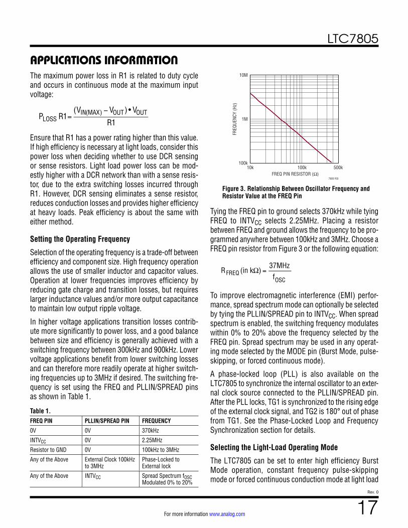
Tying the FREQ pin to ground selects 370kHz while tying FREQ to INTVCC selects 2.25MHz. Placing a resistor between FREQ and ground allows the frequency to be pro-grammed anywhere between 100kHz and 3MHz. Choose a FREQ pin resistor from Figure 3 or the following equation:
R (in kΩ)FREQ =
37MHzfOSC
To improve electromagnetic interference (EMI) perfor-mance, spread spectrum mode can optionally be selected by tying the PLLIN/SPREAD pin to INTVCC. When spread spectrum is enabled, the switching frequency modulates within 0% to 20% above the frequency selected by the FREQ pin. Spread spectrum may be used in any operat-ing mode selected by the MODE pin (Burst Mode, pulse-skipping, or forced continuous mode).
A phase-locked loop (PLL) is also available on the LTC7805 to synchronize the internal oscillator to an exter-nal clock source connected to the PLLIN/SPREAD pin. After the PLL locks, TG1 is synchronized to the rising edge of the external clock signal, and TG2 is 180° out of phase from TG1. See the Phase-Locked Loop and Frequency Synchronization section for details.
Selecting the Light-Load Operating Mode
The LTC7805 can be set to enter high efficiency Burst Mode operation, constant frequency pulse-skipping mode or forced continuous conduction mode at light load
APPLICATIONS INFORMATION
Figure 3. Relationship Between Oscillator Frequency and Resistor Value at the FREQ Pin
FREQ PIN RESISTOR (Ω)10k 100k 500k
100k
1M
10M
FREQ
UENC
Y (H
z)
7805 F03

LTC7805
18Rev. 0
For more information www.analog.com
currents. To select Burst Mode operation, tie the MODE to ground. To select forced continuous operation, tie the MODE pin to INTVCC. To select pulse-skipping mode, tie the MODE pin to INTVCC through a 100k resistor. An inter-nal 100k resistor from the MODE pin to ground selects Burst Mode if the pin is floating. When synchronized to an external clock through the PLLIN/SPREAD pin, the LTC7805 operates in pulse-skipping mode if it is selected, or in forced continuous mode otherwise. Table 2 sum-marizes the use of the MODE pin to select the light load operating mode.
Table 2.
MODE PINLIGHT-LOAD OPERATING MODE
MODE WHEN SYNCHRONIZED
0V or Floating Burst Mode Forced Continuous
100k to INTVCC Pulse-Skipping Pulse-Skipping
INTVCC Forced Continuous Forced Continuous
In general, the requirements of each application will dictate the appropriate choice for light-load operating mode. In Burst Mode operation, the inductor current is not allowed to reverse. The reverse current comparator turns off the bottom MOSFET just before the inductor current reaches zero, preventing it from reversing and going negative. Thus, the regulator operates in discon-tinuous operation. In addition, when the load current is very light, the inductor current will begin bursting at fre-quencies lower than the switching frequency and enter a low current sleep mode when not switching. As a result, Burst Mode operation has the highest possible efficiency at light load.
In forced continuous mode, the inductor current is allowed to reverse at light loads and switches at the same frequency regardless of load. In this mode, the efficiency at light loads is considerably lower than in Burst Mode operation. However, continuous operation has the advan-tage of lower output voltage ripple and less interference to audio circuitry. In forced continuous mode, the output ripple is independent of load current.
In pulse-skipping mode, constant frequency operation is maintained down to approximately 1% of designed maximum output current. At very light loads, the PWM
comparator may remain tripped for several cycles and force the top MOSFET to stay off for the same number of cycles (i.e., skipping pulses). The inductor current is not allowed to reverse (discontinuous operation). This mode, like forced continuous operation, exhibits low output rip-ple as well as low audio noise and reduced RF interference as compared to Burst Mode operation. It provides higher light load efficiency than forced continuous mode, but not nearly as high as Burst Mode operation. Consequently, pulse-skipping mode represents a compromise between light load efficiency, output ripple and EMI.
In some applications, it may be desirable to change light load operating mode based on the conditions present in the system. For example, if a system is inactive, one might select high efficiency Burst Mode operation by keeping the MODE pin set to 0V. When the system wakes, one might send an external clock to PLLIN/SPREAD, or tie MODE to INTVCC to switch to low noise forced continuous mode. Such on-the-fly mode changes can allow an individual application to benefit from the advantages of each light load operating mode.
Power MOSFET Selection
Two external power MOSFETs must be selected for each controller in the LTC7805: one N-channel MOSFET for the top (main) switch and one N-channel MOSFET for the bottom (synchronous) switch. The peak-to-peak gate drive levels are set by the INTVCC regulation point of 5.4V. Consequently, logic level threshold MOSFETs must be used in most applications. Pay close attention to the BVDSS specification for the MOSFETs as well; many of the logic level MOSFETs are limited to 30V or less.
Selection criteria for the power MOSFETs include the on resistance RDS(ON), Miller capacitance CMILLER, input volt-age, and maximum output current. Miller capacitance, CMILLER, can be approximated from the gate charge curve usually provided on the MOSFET manufacturers’ data sheet. CMILLER is equal to the increase in gate charge along the horizontal axis while the curve is approximately flat divided by the specified change in VDS. This result is then multiplied by the ratio of the application applied VDS to the gate charge curve specified VDS. When the IC is
APPLICATIONS INFORMATION
LTC7805
19Rev. 0
For more information www.analog.com
operating in continuous mode the duty cycles for the top and bottom MOSFETs are given by:
MAIN SWITCH DUTY CYCLE =VOUT
VIN
SYNCHRONOUS SWITCH DUTY CYCLE =– VOUT
VIN
VIN
The MOSFET power dissipations at maximum output cur-rent are given by:
PMAIN =VOUT
VINIMAX( )
21+ δ( )RDS(ON) +
(VIN)2 IMAX
2
⎛
⎝⎜
⎞
⎠⎟(RDR )(CMILLER ) •
1
VINTVCC − VTHMIN+
1
VTHMIN
⎡
⎣⎢
⎤
⎦⎥(f)
PSYNC =VIN − VOUT
VINIMAX( )
21+ δ( )RDS(ON)
where δ is the temperature dependency of RDS(ON) (δ ≈ 0.005/°C) and RDR is the effective driver resistance at the MOSFET’s Miller threshold voltage (RDR ≈ 2Ω). VTHMIN is the typical MOSFET minimum threshold voltage.
Both MOSFETs have I2R losses while the main N-channel equations include an additional term for transition losses, which are highest at high input voltages. For VIN < 20V the high current efficiency generally improves with larger MOSFETs, while for VIN > 20V the transition losses rap-idly increase to the point that the use of a higher RDS(ON) device with lower CMILLER actually provides higher effi-ciency. The synchronous MOSFET losses are greatest at high input voltage when the top switch duty factor is low or during a short-circuit when the synchronous switch is on close to 100% of the period.
CIN and COUT Selection
The selection of CIN is simplified by the 2-phase archi-tecture and its impact on the worst-case RMS current drawn through the input network (battery/fuse/capaci-tor). It can be shown that the worst-case capacitor RMS
current occurs when only one controller is operating. The controller with the highest VOUT • IOUT product needs to be used in the equation below to determine the maximum RMS capacitor current requirement.
Increasing the output current drawn from the other con-troller will actually decrease the input RMS ripple current from its maximum value. The out-of-phase technique typi-cally reduces the input capacitor’s RMS ripple current by a factor of 30% to 70% when compared to a single-phase power supply solution.
In continuous mode, the source current of the top MOSFET is a square wave of duty cycle VOUT/VIN. To pre-vent large voltage transients, a low ESR capacitor sized for the maximum RMS current of one channel must be used. At maximum load current IMAX, the maximum RMS capacitor current is given by:
CIN Required IRMS ≈
IMAX
VINVOUT( ) VIN − VOUT( )⎡⎣ ⎤⎦
1/2
This formula has a maximum at VIN = 2VOUT, where IRMS = IOUT/2. This simple worst-case condition is commonly used for design because even significant deviations do not offer much relief. Note that capacitor manufacturers’ ripple current ratings are often based on only 2000 hours of life. This makes it advisable to further derate the capaci-tor, or to choose a capacitor rated at a higher temperature than required. Several capacitors may be paralleled to meet size or height requirements in the design. Due to the high operating frequency of the LTC7805, ceramic capacitors can also be used for CIN. Always consult the manufacturer if there is any question.
The benefit of the LTC7805 2-phase operation can be calculated by using this equation for the higher power controller and then calculating the loss that would have resulted if both controller channels switched on at the same time. The total RMS power lost is lower when both controllers are operating due to the reduced overlap of current pulses required through the input capacitor’s ESR. This is why the input capacitor’s requirement cal-culated above for the worst-case controller is adequate for the dual controller design. Also, the input protection fuse resistance, battery resistance, and PC board trace resistance losses are also reduced due to the reduced
APPLICATIONS INFORMATION

LTC7805
20Rev. 0
For more information www.analog.com
peak currents in a 2-phase system. The overall benefit of a multiphase design will only be fully realized when the source impedance of the power supply/battery is included in the efficiency testing.
The drains of the top MOSFETs should be placed within 1cm of each other and share a common CIN(s). Separating the drains and CIN may produce undesirable resonances at VIN.
A small (0.1μF to 1μF) bypass capacitor between the chip VIN pin and ground, placed close to the LTC7805, is also suggested. An optional 1Ω to 10Ω resistor placed between CIN and the VIN pin provides further isolation from a noisy input supply.
The selection of COUT is driven by the effective series resistance (ESR). Typically, once the ESR requirement is satisfied, the capacitance is adequate for filtering. The output ripple (ΔVOUT) is approximated by:
ΔVOUT ≈ ΔIL ESR +
18fCOUT
⎛
⎝⎜
⎞
⎠⎟
where f is the operating frequency, COUT is the output capacitance and ΔIL is the ripple current in the inductor. The output ripple is highest at maximum input voltage since ΔIL increases with input voltage.
Setting the Output Voltage
The LTC7805 output voltages are each set by an external feedback resistor divider carefully placed across the out-put, as shown in Figure 4. The regulated output voltage is determined by:
VOUT = 0.8V 1+
R
RB
A
⎛
⎝⎜
⎞
⎠⎟
Place resistors RA and RB very close to the VFB pin to minimize PCB trace length and noise on the sensitive VFB node. Great care should be taken to route the VFB trace away from noise sources, such as the inductor or the SW trace. To improve frequency response, a feedforward capacitor (CFF) may be used.
For applications with multiple output voltage levels, select channel 1 to be the lowest output voltage that is greater than 3.2V. When the SENSE1– pin (connected to VOUT1) is above 3.2V, it biases some internal circuitry instead of VIN, thereby increasing light load Burst Mode efficiency. Similarly, connect EXTVCC to the lowest output voltage that is greater than the 4.8V maximum EXTVCC rising switch-over threshold. EXTVCC then supplies the high current gate drivers and relieves additional quiescent current from VIN, further reducing the VIN pin current to ≈1μA in sleep.
RUN Pins and Undervoltage Lockout
The two channels of the LTC7805 are enabled using the RUN1, and RUN2 pins. The RUN pins have a rising threshold of 1.2V with 100mV of hysteresis. Pulling a RUN pin below 1.1V shuts down the main control loop and resets the soft-start for that channel. Pulling both RUN pins below 0.7V disables the controllers and most internal circuits, including the INTVCC LDOs. In this state, the LTC7805 draws only ≈1.5μA of quiescent current.
The RUN pins are high impedance and must be externally pulled up/down or driven directly by logic. Each RUN pin can tolerate up to 40V (absolute maximum), so it can be conveniently tied to VIN in always-on applications where the controller is enabled continuously and never shut down. Do not float the RUN pins.
The RUN pins can also be configured as precise under-voltage lockouts (UVLOs) on the input supply with a resis-tor divider from VIN to ground, as shown in Figure 5.
APPLICATIONS INFORMATION
Figure 4. Setting Output Voltage
7805 F04
1/2 LTC7805
VFB
RB CFF
RA
VOUT
Figure 5. Using the RUN Pins As a UVLD
7805 F06
1/2 LTC7805
RUN
R1
R2
VIN

LTC7805
21Rev. 0
For more information www.analog.com
The VIN UVLO thresholds can be computed as:
UVLO RISING = 1.2V 1+R
R1
2
⎛
⎝⎜
⎞
⎠⎟
UVLO FALLING = 1.1V 1+R
R1
2
⎛
⎝⎜
⎞
⎠⎟
The current that flows through the R1-R2 divider directly adds to the shutdown, sleep, and active current of the LTC7805, and care should be taken to minimize the impact of this current on the overall efficiency of the application circuit. Resistor values in the MΩ range may be required to keep the impact on quiescent shutdown and sleep cur-rents low.
Soft-Start and Tracking (TRACK/SS Pins)
The start-up of each VOUT is controlled by the voltage on the TRACK/SS pin (TRACK/SS1 for channel 1, TRACK/SS2 for channel 2). When the voltage on the TRACK/SS pin is less than the internal 0.8V reference, the LTC7805 regulates the VFB pin voltage to the voltage on the TRACK/SS pin instead of the internal reference. The TRACK/SS pin can be used to program an external soft-start function or to allow VOUT to track another supply during start-up.
Soft-start is enabled by simply connecting a capacitor from the TRACK/SS pin to ground. An internal 12.5μA current source charges the capacitor, providing a linear ramping voltage at the TRACK/SS pin. The LTC7805 will regulate its feedback voltage (and hence VOUT) accord-ing to the voltage on the TRACK/SS pin, allowing VOUT to rise smoothly from 0V to its final regulated value. For a desired soft-start time, tSS, select a soft-start capacitor CSS = tSS • 15μF/sec.
Alternatively, the TRACK/SS pins can be used to track two or more supplies during start-up, as shown qualitatively in Figure 6a and Figure 6b. To do this, a resistor divider should be connected from the master supply (VX) to the TRACK/SS pin of the slave supply (VOUT), as shown in Figure 7. During start-up VOUT will track VX according to the ratio set by the resistor divider:
VXVOUT
=RA
RTRACKA•RTRACKA +RTRACKB
RA +RB
Set RTRACKA = RA and RTRACKB = RB for coincident track-ing (VOUT = VX during start-up).
Single Output 2-Phase Operation
For high power applications, the two channels can be operated in a 2-phase single output configuration. The
APPLICATIONS INFORMATION
Figure 6. Two Different Modes of Output Voltage Tracking
Figure 7. Using the TRACK/SS Pin for Tracking
7805 F06a
VX(MASTER)
VOUT(SLAVE)
OUTP
UT (V
OUT)
TIME
(a) Coincident Tracking
7805 F06b
VX(MASTER)
VOUT(SLAVE)
OUTP
UT (V
OUT)
TIME
(b) Ratiometric Tracking
7805 F07
LTC7805
VFB
TRACK/SS1,2
RB
RA
VOUT
RTRACKB
RTRACKA
VX

LTC7805
22Rev. 0
For more information www.analog.com
channels switch 180° out-of-phase, which reduces the required output capacitance in addition to the required input capacitance and power supply induced noise. To configure the LTC7805 for 2-phase operation, tie VFB2 to INTVCC, ITH2 to ground, and RUN2 to RUN1.
The RUN1, VFB1, ITH1, TRACK/SS1 pins are then used to control both channels, but each channel uses its own ICMP and IR comparators to monitor their respective inductor currents. Figure 10 is a typical application con-figured for single output 2-phase operation.
INTVCC Regulators
The LTC7805 features two separate internal low dropout linear regulators (LDOs) that supply power at the INTVCC pin from either the VIN pin or the EXTVCC pin depending on the EXTVCC pin voltage. INTVCC powers the MOSFET gate drivers and most of the internal circuitry. The VIN LDO and the EXTVCC LDO each regulate INTVCC to 5.4V and can provide a peak current of at least 100mA.
The INTVCC pin must be bypassed to ground with a minimum of 4.7μF ceramic capacitor, placed as close as possible to the pin. An additional 1μF ceramic capacitor placed directly adjacent to the INTVCC and GND pins is also highly recommended to supply the high frequency transient currents required by the MOSFET gate drivers.
High input voltage applications in which large MOSFETs are being driven at high frequencies may cause the maxi-mum junction temperature rating for the LTC7805 to be exceeded. The INTVCC current, which is dominated by the gate charge current, may be supplied by either the VIN LDO or the EXTVCC LDO. When the voltage on the EXTVCC pin is less than 4.8V, the VIN LDO is enabled. Power dissi-pation for the IC in this case is equal to VIN • IINTVCC. The gate charge current is dependent on operating frequency as discussed in the Efficiency Considerations section. The junction temperature can be estimated by using the equa-tions given in Note 2 of the Electrical Characteristics. For example, the LTC7805 INTVCC current is limited to less than 35mA from a 36V supply when not using the EXTVCC supply at a 70°C ambient temperature:
TJ = 70°C + (35mA)(36V)(43°C/W) = 125°C
To prevent the maximum junction temperature from being exceeded, the input supply current must be checked while operating in continuous conduction mode (MODE = INTVCC) at maximum VIN.
When the voltage applied to EXTVCC rises above 4.8V, the VIN LDO is turned off and the EXTVCC LDO is enabled. The EXTVCC LDO remains on as long as the voltage applied to EXTVCC remains above approximately 4.5V. The EXTVCC LDO attempts to regulate the INTVCC voltage to 5.4V, so while EXTVCC is less than 5.4V, the LDO is in dropout and the INTVCC voltage is approximately equal to EXTVCC. When EXTVCC is greater than 5.4V (up to an absolute maximum of 30V), INTVCC is regulated to 5.4V. Using the EXTVCC LDO allows the MOSFET driver and control power to be derived from one of the LTC7805’s switch-ing regulator outputs (4.8V ≤ VOUT ≤ 30V) during normal operation and from the VIN LDO when the output is out of regulation (e.g., start-up, short-circuit). If more current is required through the EXTVCC LDO than is specified, an external Schottky diode can be added between the EXTVCC and INTVCC pins. In this case, do not apply more than 6V to the EXTVCC pin.
Significant efficiency and thermal gains can be realized by powering INTVCC from an output, since the VIN cur-rent resulting from the driver and control currents will be scaled by a factor of VOUT/(VIN • Efficiency). For 5V to 30V regulator outputs, this means connecting the EXTVCC pin directly to VOUT. Tying the EXTVCC pin to an 8.5V supply reduces the junction temperature in the previous example from 125°C to:
TJ = 70°C + (35mA)(8.5V)(43°C/W) = 83°C
However, for 3.3V and other low voltage outputs, addi-tional circuitry is required to derive INTVCC power from the output.
The following list summarizes the four possible connec-tions for EXTVCC:
1. EXTVCC grounded. This will cause INTVCC to be pow-ered from the internal VIN LDO resulting in an efficiency penalty of up to 10% or more at high input voltages.
APPLICATIONS INFORMATION

LTC7805
23Rev. 0
For more information www.analog.com
2. EXTVCC connected directly to one of the regulator out-puts. This is the normal connection for an application with an output in the range of 5V to 30V and provides the highest efficiency. If both outputs are in the 5V to 30V range, connect EXTVCC to the lesser of the two outputs to maximize efficiency.
3. EXTVCC connected to an external supply. If an external supply is available, it may be used to power EXTVCC provided that it is compatible with the MOSFET gate drive requirements. This supply may be higher or lower than VIN; however, a lower EXTVCC voltage results in higher efficiency.
4. EXTVCC connected to an output-derived boost or charge pump. For regulators where both outputs are below 5V, efficiency gains can still be realized by connect-ing EXTVCC to an output-derived voltage that has been boosted to greater than 4.8V.
Topside MOSFET Driver Supply (CB, DB)
External bootstrap capacitors CB connected to the BOOST pins supply the gate drive voltages for the top-side MOSFETs. Capacitor CB in the Functional Diagram is charged though external diode DB from INTVCC when the SW pin is low.
When one of the topside MOSFETs is to be turned on, the driver places the CB voltage across the gate-source of the desired MOSFET. This enhances the MOSFET and turns on the topside switch. The switch node voltage, SW, rises to VIN and the BOOST pin follows. With the topside MOSFET on, the boost voltage is above the input supply: VBOOST = VIN + VINTVCC. The value of the boost capacitor CB needs to be 100 times that of the total input capacitance of the topside MOSFET(s). For a typical application, a value of CB = 0.1μF is generally sufficient.
The external diode DB can be a Schottky diode or sili-con diode, but in either case it should have low leakage and fast recovery. The reverse breakdown of the diode must be greater than VIN(MAX). Pay close attention to the reverse leakage at high temperatures where it generally increases substantially.
A leaky diode not only increases the quiescent current of the regulator, but it can create current path from the BOOST pin to INTVCC. This will cause INTVCC to rise if
the diode leakage exceeds the current consumption on INTVCC, which is primarily a concern in Burst Mode opera-tion where the load on INTVCC can be very small. There is an internal voltage clamp on INTVCC that prevents the INTVCC voltage from running away, but this clamp should be regarded as a failsafe only.
The topside MOSFET driver for each channel includes an internal charge pump that delivers current to the boot-strap capacitor from the BOOST pin. This charge cur-rent maintains the bias voltage required to keep the top MOSFET on continuously during dropout conditions. Curves displaying the available charge pump current under different operating conditions can be found in the Typical Performance Characteristics section.
Minimum On-Time Considerations
Minimum on-time tON(MIN) is the smallest time duration that the LTC7805 is capable of turning on the top MOSFET. It is determined by internal timing delays and the gate charge required to turn on the MOSFET. Low duty cycle applications may approach this minimum on time limit and care should be taken to ensure that:
V • f
VOUTt <ON(MIN)IN OSC
If the duty cycle falls below what can be accommodated by the minimum on-time, the controller will begin to skip cycles. The output voltage will continue to be regulated, but the ripple voltage and current will increase. The mini-mum on-time for the LTC7805 is approximately 40ns. However, as the peak sense voltage decreases the mini-mum on-time gradually increases up to about 60ns. This is of particular concern in forced continuous applications with low ripple current at light loads. If the duty cycle drops below the minimum on-time limit in this situation, a significant amount of cycle skipping can occur with cor-respondingly larger current and voltage ripple.
Fault Conditions: Current Limit and Foldback
The LTC7805 includes current foldback to reduce the load current when the output is shorted to ground. If the output voltage falls below 50% of its regulation point, then the maximum sense voltage is progressively lowered from
APPLICATIONS INFORMATION
LTC7805
24Rev. 0
For more information www.analog.com
100% to 40% of its maximum value. Under short-circuit conditions with very low duty cycles, the LTC7805 will begin cycle skipping to limit the short circuit current. In this situation the bottom MOSFET dissipates most of the power but less than in normal operation. The short-circuit ripple current is determined by the minimum on-time, tON(MIN) ≈ 40ns, the input voltage and inductor value:
ΔIL(SC) = tON(MIN) • VIN/L
The resulting average short-circuit current is:
ISC = 40% • ILIM(MAX) − ΔIL(SC)/2
Fault Conditions: Overvoltage Protection (Crowbar)
The overvoltage crowbar is designed to blow a system input fuse when the output voltage of the regulator rises much higher than nominal levels. The crowbar causes huge currents to flow that blow the fuse to protect against a shorted top MOSFET if the short occurs while the con-troller is operating.
If an output voltage rises 10% above the set regula-tion point, the top MOSFET is turned off and the bottom MOSFET is turned on until the overvoltage condition is cleared. The bottom MOSFET remains on continuously for as long as the overvoltage condition persists; if VOUT returns to a safe level, normal operation automatically resumes.
A shorted top MOSFET will result in a high current con-dition which will open the system fuse. The switching regulator will regulate properly with a leaky top MOSFET by altering the duty cycle to accommodate the leakage.
Fault Conditions: Overtemperature Protection
At higher temperatures, or in cases where the internal power dissipation causes excessive self-heating (such as a short from INTVCC to ground) internal overtemperature shutdown circuitry will shut down the LTC7805. When the internal die temperature exceeds 180°C, the INTVCC LDO and gate drivers are disabled. When the die cools to 160°C, the LTC7805 enables the INTVCC LDO and resumes opera-tion beginning with a soft-start startup. Long-term over-stress (TJ > 125°C) should be avoided as it can degrade the performance or shorten the life of the part.
Phase-Locked Loop and Frequency Synchronization
The LTC7805 has an internal phase-locked loop (PLL) which allows the turn-on of the top MOSFET of control-ler 1 to be synchronized to the rising edge of an external clock signal applied to the PLLIN/SPREAD pin. The turn on of controller 2’s top MOSFET is thus 180° out of phase with the external clock.
Rapid phase-locking can be achieved by using the FREQ pin to set a free-running frequency near the desired synchronization frequency. Before synchronization, the PLL is prebiased to the frequency set by the FREQ pin. Consequently, the PLL only needs to make minor adjustments to achieve phase-lock and synchronization. Although it is not required that the free-running frequency be near the external clock frequency, doing so will pre-vent the oscillator from passing through a large range of frequencies as the PLL locks.
When synchronized to an external clock, the LTC7805 operates in pulse-skipping mode if it is selected by the MODE pin, or in forced continuous mode otherwise. The LTC7805 is guaranteed to synchronize to an external clock applied to the PLLIN/SPREAD pin that swings up to at least 2.2V and down to 0.5V or less. Note that the LTC7805 can only be synchronized to an external clock frequency within the range of 100kHz to 3MHz.
Efficiency Considerations
The percent efficiency of a switching regulator is equal to the output power divided by the input power times 100%. It is often useful to analyze individual losses to determine what is limiting the efficiency and which change would produce the most improvement. Percent efficiency can be expressed as:
%Efficiency = 100% – (L1 + L2 + L3 + ...)
where L1, L2, etc. are the individual losses as a percent-age of input power.
Although all dissipative elements in the circuit produce losses, four main sources usually account for most of the losses in LTC7805 circuits: 1) IC VIN current, 2) INTVCC regulator current, 3) I2R losses, 4) Topside MOSFET tran-sition losses.
APPLICATIONS INFORMATION

LTC7805
25Rev. 0
For more information www.analog.com
1. The VIN current is the DC supply current given in the Electrical Characteristics table, which excludes MOSFET driver and control currents. Other than at very light loads in burst mode, VIN current typically results in a small (<0.1%) loss.
2. INTVCC current is the sum of the MOSFET driver and control currents. The MOSFET driver current results from switching the gate capacitance of the power MOSFETs. Each time a MOSFET gate is switched from low to high to low again, a packet of charge, dQ, moves from INTVCC to ground. The resulting dQ/dt is a current out of INTVCC that is typically much larger than the control circuit current. In continuous mode, IGATECHG = fSW(QT + QB), where QT and QB are the gate charges of the top and bottom MOSFETs.
Supplying INTVCC from an output-derived source through EXTVCC will scale the VIN current required for the driver and control circuits by a factor of VOUT/(VIN • Efficiency). For example, in a 20V to 5V applica-tion, 10mA of INTVCC current results in approximately 2.5mA of VIN current. This reduces the mid-current loss from 10% or more (if the driver was powered directly from VIN) to only a few percent.
3. I2R losses are predicted from the DC resistances of the input fuse (if used), MOSFET, inductor, current sense resistor, and input and output capacitor ESR. In con-tinuous mode the average output current flows through L and RSENSE, but is chopped between the top and bottom MOSFETs. If the two MOSFETs have approxi-mately the same RDS(ON), then the resistance of one MOSFET can simply be summed with the resistances of L, RSENSE and ESR to obtain I2R losses.
For example, if each RDS(ON) = 30mΩ, RL = 50mΩ, RSENSE = 10mΩ and ESR = 40mΩ (sum of both input and output capacitance losses), then the total resis-tance is 130mΩ. This results in losses ranging from 3% to 13% as the output current increases from 1A to 5A for a 5V output, or a 4% to 20% loss for a 3.3V out-put. This percentage loss varies as the inverse square of VOUT for the same external components and out-put power level. The combined effects of increasingly lower output voltages and higher currents required by high performance digital systems is not doubling but
quadrupling the importance of loss terms in the switch-ing regulator system!
4. Transition losses apply only to the top MOSFETs and become significant only when operating at higher input voltages (typically 15V or greater). Transition losses can be estimated from the equation for the main switch power dissipation in the Power MOSFET Selection section.
Other hidden losses such as copper trace and internal battery resistances can account for an additional 5% to 10% efficiency degradation in portable systems. It is very important to include these system level losses during the design phase. The internal battery and fuse resistance losses can be minimized by making sure that CIN has adequate charge storage and very low ESR at the switch-ing frequency. A 25W supply will typically require a mini-mum of 20μF to 40μF of capacitance having a maximum of 20mΩ to 50mΩ of ESR. The LTC7805 2-phase archi-tecture typically halves this input capacitance requirement over competing solutions. Other losses including induc-tor core losses generally account for less than 2% total additional loss.
Checking Transient Response
The regulator loop response can be checked by looking at the load current transient response. Switching regulators take several cycles to respond to a step in DC (resistive) load current. When a load step occurs, VOUT shifts by an amount equal to ΔILOAD • (ESR), where ESR is the effective series resistance of COUT. ΔILOAD also begins to charge or discharge COUT generating the feedback error signal that forces the regulator to adapt to the current change and return VOUT to its steady-state value. During this recovery time VOUT can be monitored for excessive overshoot or ringing, which would indicate a stability problem.
OPTI-LOOP compensation allows the transient response to be optimized over a wide range of output capaci-tance and ESR values. The availability of the ITH pin not only allows optimization of control loop behavior, but it also provides a DC coupled and AC filtered closed loop response test point. The DC step, rise time and settling at this test point truly reflects the closed loop response. Assuming a predominantly second order system, phase
APPLICATIONS INFORMATION

LTC7805
26Rev. 0
For more information www.analog.com
margin and/or damping factor can be estimated using the percentage of overshoot seen at this pin. The bandwidth can also be estimated by examining the rise time at the pin. The ITH external components shown in the Typical Applications circuits provide an adequate starting point for most applications.
The ITH series RC-CC filter sets the dominant pole-zero loop compensation. The values can be modified slightly (from 0.5 to 2 times their initial values) to optimize tran-sient response once the final PC layout is done and the particular output capacitor type and value have been determined. The output capacitors need to be selected because the various types and values determine the loop gain and phase. An output current pulse of 20% to 80% of full-load current having a rise time of 1μs to 10μs will produce output voltage and ITH pin waveforms that will give a sense of the overall loop stability without breaking the feedback loop.
Placing a power MOSFET directly across the output capacitor and driving the gate with an appropriate signal generator is a practical way to produce a realistic load step condition. The initial output voltage step resulting from the step change in output current may not be within the bandwidth of the feedback loop, so this signal can-not be used to determine phase margin. This is why it is better to look at the ITH pin signal which is in the feed-back loop and is the filtered and compensated control loop response. The gain of the loop will be increased by increasing RC and the bandwidth of the loop will be increased by decreasing CC. If RC is increased by the same factor that CC is decreased, the zero frequency will be kept the same, thereby keeping the phase shift the same in the most critical frequency range of the feedback loop. The output voltage settling behavior is related to the stability of the closed-loop system and will demonstrate the actual overall supply performance.
A second, more severe transient is caused by switching in loads with large (>1μF) supply bypass capacitors. The discharged bypass capacitors are effectively put in parallel with COUT, causing a rapid drop in VOUT. No regulator can alter its delivery of current quickly enough to prevent this sudden step change in output voltage if the load switch resistance is low and it is driven quickly. If the ratio of
CLOAD to COUT is greater than 1:50, the switch rise time should be controlled so that the load rise time is limited to approximately CLOAD • 25μs/μF. Thus a 10μF capacitor would require a 250μs rise time, limiting the charging current to about 200mA.
Design Example
As a design example, assume VIN(NOMINAL) = 12V, VIN(MAX) = 22V, VOUT = 3.3V, IOUT = 20A, and fSW = 1MHz.
1. Set the operating frequency. The frequency is not one of the internal preset values, so a resistor from the FREQ pin to GND is required, with a value of:
RFREQ(in kΩ)=
37MHz1MHz
= 37kΩ
2. Determine the inductor value. Initially select a value based on an inductor ripple current of 30%. The inductor value can then be calculated from the following equation:
L= VOUT
fSW ΔIL( )1– VOUT
VIN(NOM)
⎛
⎝⎜⎜
⎞
⎠⎟⎟=0.4µH
The highest value of ripple current occurs at the maximum input voltage. In this case the ripple at VIN = 22V is 35%
3. Verify that the minimum on-time of 40ns is not violated. The minimum on-time occurs at VIN(MAX):
tON(MIN) =
VOUTVIN(MAX)(fSW)
= 150ns
This is more than sufficient to satisfy the minimum on time requirement. If the minimum on time is violated, the LTC7805 skips pulses at high input voltage, result-ing in lower frequency operation and higher inductor current ripple than desired. If undesirable, this behavior can be avoided by decreasing the frequency (with the inductor value accordingly adjusted) to avoid operation near the minimum on-time.
4. Select the RSENSE resistor value. The peak inductor current is the maximum DC output current plus half of the inductor ripple current. Or 20A • (1+0.30/2) = 23A in this case. The RSENSE resistor value can then be
APPLICATIONS INFORMATION
LTC7805
27Rev. 0
For more information www.analog.com
calculated based on the minimum value for the maxi-mum current sense threshold (43mV):
RSENSE ≤
43mV23A
≅ 2mΩ
To allow for additional margin, a lower value RSENSE may be used (for example, 1.8mΩ); however, be sure that the inductor saturation current has sufficient mar-gin above VSENSE(MAX)/RSENSE, where the maximum value of 55mV is used for VSENSE(MAX).
For this low inductor value and high current applica-tion, an RC filter into the sense pins should be used to compensate for the parasitic inductance (ESL) of the sense resistor. Assuming an RSENSE geom-etry of 1225 with a parasitic inductance of 0.2nH, the RC filter time constant should be RC = ESL/RSENSE = 0.2nH/2mΩ = 100ns, which may be imple-mented with 100Ω resistor in series with the SENSE+ pin and 1nF capacitor between SENSE+ and SENSE–.
5. Select the feedback resistors. If very light load effi-ciency is required, high value feedback resistors may be used to minimize the current due to the feedback divider. However, in most applications a feedback divider current in the range of 10μA to 100μA or more is acceptable. For a 50μA feedback divider current, RA = 0.8V/50μA = 16kΩ. RB can then be calculated as RB = RA(3.3V/0.8V – 1) = 50kΩ.
6. Select the MOSFETs. The best way to evaluate MOSFET performance in a particular application is to build and test the circuit on the bench, facilitated by an LTC7805 demo board. However, an educated guess about the application is helpful to initially select MOSFETs. Since this is a high current, low voltage application, I2R losses will likely dominate over transition losses for the top MOSFET. Therefore, choose a MOSFET with lower RDS(ON) as opposed to lower gate charge to minimize the combined loss terms. The bottom MOSFET does not experience transition losses, and its power loss is generally dominated by I2R losses. For this reason, the bottom MOSFET is typically chosen to be of lower RDS(ON) and subsequently higher gate charge than the top MOSFET.
Due to the high current in this application, two MOSFETs may be needed in parallel to more evenly balance the dissipated power and to lower the RDS(ON). Be sure to select logic-level threshold MOSFETs, since the gate drive voltage is limited to 5.4V (INTVCC).
7. Select the input and output capacitors. CIN is chosen for an RMS current rating of at least 10A (IOUT/2, with margin) at temperature assuming only this channel is on. COUT is chosen with an ESR of 3mΩ for low output ripple. Multiple capacitors connected in parallel may be required to reduce the ESR to this level. The output ripple in continuous mode will be highest at the maximum input voltage. The output voltage ripple due to ESR is approximately:
VORIPPLE = ESR • ΔIL = 3mΩ • 6A = 18mVP-P
On the 3.3V output, this is equal to 0.55% of peak to peak voltage ripple.
8. Determine the bias supply components. Since the regu-lated output is not greater than the EXTVCC switchover threshold (4.8V), it cannot be used to bias INTVCC. However, if another supply is available, for example if the other channel is regulating to 5V, connect that supply to EXTVCC to improve the efficiency.
For a 6.5ms soft-start, select a 0.1μF capacitor for the TRACK/SS pin. As a first pass estimate for the bias components, select CINTVCC = 4.7μF, boost supply capacitor CB = 0.1μF and low forward drop boost sup-ply diode CMDSH-4E from Central Semiconductor.
9. Determine and set application-specific parameters. Set the MODE pin based on the trade-off of light load efficiency and constant frequency operation. Set the PLLIN/SPREAD pin based on whether a fixed, spread spectrum, or phase-locked frequency is desired. The RUN pin can be used to control the minimum input voltage for regulator operation or can be tied to VIN for always-on operation. Use ITH compensation com-ponents from the typical applications as a first guess, check the transient response for stability, and modify as necessary.
APPLICATIONS INFORMATION

LTC7805
28Rev. 0
For more information www.analog.com
PC Board Layout Checklist
When laying out the printed circuit board, the following checklist should be used to ensure proper operation of the IC. Figure 8 illustrates the current waveforms present in the various branches of the synchronous regulators operating in the continuous mode. Check the following in your layout:
1. Are the top N-channel MOSFETs located within 1cm of each other with a common drain connection at CIN? Decoupling capacitors for the two channels should be close to each other to avoid a large resonant loop.
2. Are the signal and power grounds kept separate? The combined IC ground pin and the ground return of CINTVCC must return to the combined COUT (–) ter-minals. The area of the “hot loop” formed by the top N-channel MOSFET, bottom N-channel MOSFET and the high-frequency (ceramic) input capacitors, as shown in Figure 8, should be minimized with short leads, pla-nar connections, and multiple paralleled vias where needed. The output capacitor (–) terminals should be connected as close as possible to the (–) terminals of the input capacitor.
3. Do the LTC7805 VFB pins’ resistive dividers connect to the (+) terminals of COUT? The resistive divider must be connected between the (+) terminal of COUT and signal ground. Place the divider close to the VFB pin to minimize noise coupling into the sensitive VFB node. The feedback resistor connections should not be along the high current input feeds from the input capacitor(s).
4. Are the SENSE– and SENSE+ leads routed together with minimum PC trace spacing? Route these traces away from the high frequency switching nodes, on an inner layer if possible. The filter capacitor between SENSE+ and SENSE– should be as close as possible to the IC. Ensure accurate current sensing with Kelvin connec-tions at the sense resistor.
5. Is the INTVCC decoupling capacitor connected close to the IC, between the INTVCC and the power ground pin? This capacitor carries the MOSFET drivers’ cur-rent peaks. An additional 1μF ceramic capacitor placed immediately next to the INTVCC and GND pins can help improve noise performance substantially. The boost
diodes should have separate routes directly to the INTVCC capacitor near the IC, not shared with any sig-nal connections to INTVCC.
6. Keep the switching nodes (SW1, SW2), top gate nodes (TG1, TG2), and boost nodes (BOOST1, BOOST2) away from sensitive small-signal nodes, especially from the other channel’s voltage and current sensing feedback pins. All of these nodes have very large and fast-moving signals and therefore should be kept on the output side of the LTC7805 and occupy minimum PC trace area. Minimize the inductance of the TG and BG gate drive traces and their respective return paths to the control-ler IC (SW and GND) by using wide traces and multiple parallel vias.
7. Use a modified star ground technique: a low imped-ance, large copper area central grounding point on the same side of the PC board as the input and output capacitors with tie-ins for the bottom of the INTVCC decoupling capacitor, the bottom of the voltage feed-back resistive divider and the GND pin of the IC.
For more detailed layout guidance, see Analog Devices Application Notes AN136 “PCB Layout Considerations for Non-Isolated Switching Power Supplies” and AN139 “Power Supply Layout and EMI”.
PC Board Layout Debugging
Start with one controller on at a time. It is helpful to use a DC-50MHz current probe to monitor the current in the inductor while testing the circuit. Monitor the output switching node (SW pin) to synchronize the oscilloscope to the internal oscillator and probe the actual output volt-age as well. Check for proper performance over the oper-ating voltage and current range expected in the applica-tion. The frequency of operation should be maintained over the input voltage range down to dropout and until the output load drops below the low current operation threshold—typically 25% of the maximum designed cur-rent level in Burst Mode operation.
The duty cycle percentage should be maintained from cycle to cycle in a well-designed, low noise PCB imple-mentation. Variation in the duty cycle at a subharmonic rate can suggest noise pickup at the current or volt-age sensing inputs or inadequate loop compensation.
APPLICATIONS INFORMATION

LTC7805
29Rev. 0
For more information www.analog.com
Overcompensation of the loop can be used to tame a poor PC layout if regulator bandwidth optimization is not required. Only after each controller is checked for its indi-vidual performance should both controllers be turned on at the same time. A particularly difficult region of opera-tion is when one controller channel is nearing its current comparator trip point when the other channel is turning on its top MOSFET. This occurs around 50% duty cycle on either channel due to the phasing of the internal clocks and may cause minor duty cycle jitter.
Reduce VIN from its nominal level to verify operation of the regulator in dropout. Check the operation of the undervoltage lockout circuit by further lowering VIN while monitoring the outputs to verify operation. Investigate whether any problems exist only at higher output cur-rents or only at higher input voltages. If problems coincide with high input voltages and low output currents, look for capacitive coupling between the BOOST, SW, TG, and pos-sibly BG connections and the sensitive voltage and current pins. The capacitor placed across the current sensing pins
needs to be placed immediately adjacent to the pins of the IC. This capacitor helps to minimize the effects of dif-ferential noise injection due to high frequency capacitive coupling. If problems are encountered with high current output loading at lower input voltages, look for inductive coupling between CIN, the top MOSFET, and the bottom MOSFET components to the sensitive current and voltage sensing traces. In addition, investigate common ground path voltage pickup between these components and the GND pin of the IC.
An embarrassing problem, which can be missed in an otherwise properly working switching regulator, results when the current sensing leads are hooked up backwards. The output voltage under this improper hookup will still be maintained but the advantages of current mode control will not be realized. Compensation of the voltage loop will be much more sensitive to component selection. This behavior can be investigated by temporarily shorting out the current sensing resistor—don’t worry, the regulator will still maintain control of the output voltage.
APPLICATIONS INFORMATION
RL1
L1SW1 RSENSE1 VOUT1
COUT1
VIN
CINRIN
RL2BOLD LINES INDICATEHIGH SWITCHING CURRENT. KEEP LINESTO A MINIMUM LENGTH.
L2SW2
7805 F08
RSENSE2 VOUT2
COUT2HOT LOOP
HOT LOOP
Figure 8. Branch Current Waveforms for Bucks

LTC7805
30Rev. 0
For more information www.analog.com
TYPICAL APPLICATIONS
Figure 9. High Efficiency Dual 3.3V, 5V Step-Down Regulator with Spread Spectrum
0.1µF
D1 D2
L10.9µH
MTOP1 MTOP2
3mΩ
MBOT2MBOT1
0.1µFL2
1.8µH
100µF×2
2mΩ
210k
68.1k
7805 F09a
LTC7805
RUN1 RUN2
SW1
BG1
TG1
BOOST1
SENSE1–
VIN
INTVCC
VIN4.5V TO 38V
VOUT13.3V, 12A VOUT2
5V*, 10A
SENSE1+
SENSE2–
MODE
TRACK/SS2
ITH2
EXTVCC
VFB2
PLLIN/SPREAD
SENSE2+
SW2
BG2
TG2
BOOST2
VFB1
PGOOD2PGOOD1
INTVCC
ITH1
TRACK/SS1
FREQ
GND
357k
68.1k
0.1µF
3.3nF
11k
100pF
3.3nF
4.5k 0.1µF
4.7µFfSW = 370kHz
CIN100µF63V
10µF×3
+INTVCC
COUT1330µF6.3V
+
100pF
100µF×2
COUT2330µF6.3V
+
1nF1nF
20Ω
L1: WURTH 744355090L2: WURTH 744313180MTOP1,2: INFINEON BSC059N04LS6MBOT1,2: INFINEON BSC022N04LS
D1,2: CENTRAL SEMI CMDSH-4ECIN: SUNCON 63CE100LXCOUT1,2: KEMET T520V337M006ATE015*VOUT2 FOLLOWS VIN WHEN VIN < 5V
Efficiency vs Load CurrentNo-Load Burst Mode Input Current vs Input Voltage Short-Circuit Response
VOUT1 = 3.3V VOUT2 = 5V
BOTH CHANNELS ONBurst Mode OPERATION
VIN = 12V VIN = 24V VIN = 36V
VIN = 12VVIN = 24VVIN = 36V
LOAD CURRENT (A)0 3 6 9 12
70
75
80
85
90
95
100
EFFI
CIEN
CY (%
)
7805 F09b
CHANNEL 1 ONCHANNEL 2 ONBOTH CHANNELS ON
VIN VOLTAGE (V)5 10 15 20 25 30 35 40
0
5
10
15
20
25
30
35
40
45
50
V IN
CURR
ENT
(µA)
vs Input Voltage
7805 F09c
VIN = 12V FORCED CONTINUOUS MODE
100µs/DIV7805 F09d
VOUT25V/DIV
INDUCTORCURRENT
5A/DIV

LTC7805
31Rev. 0
For more information www.analog.com
TYPICAL APPLICATIONS
Figure 10. 2.25MHz 2-Phase Single Output 3.3V, 24A Step-Down Regulator
D1
MTOP1
3mΩ
MBOT1
0.1µF
1nF
1nF
L1, 0.16µH
7805 F10a
LTC7805
RUN1
RUN2
VFB2
MODE
FREQ
INTVCC
INTVCC
VIN
VIN4.5V TO 38V
12V NOMINAL
VOUT3.3V, 24A
SENSE1–
BOOST2
VFB1
TG2
SW2
BG2
ITH1
TRACK/SS1
PGOOD1
PGOOD2
ITH2
TRACK/SS2
PLLIN/SPREAD
SENSE1+
SW1
BG1
TG1BOOST1
GND
210k
68.1k
0.1µF
47pF
470pF
10k
3mΩ
SENSE2+
SENSE2–
100µF10µF×6
+
INTVCC
VIN
D2
MTOP2
MBOT2
0.1µF L2, 0.16µH
INTVCC
VIN
COUT470µF4V
4.7µF×6
+
4.7µF
EXTVCC
150Ω
150Ω
fSW = 2.25MHzMTOP1,2: INFINEON BSC059N04LS6MBOT1,2: INFINEON BSC032N04LSL1,2: COILCRAFT XAL5030-161MED1,2: INFINEON BAS140WE6327HTSA1COUT: KEMET T520D477M004ATE012
Load Step Transient Response Efficiency vs Load Current Output Voltage Noise Spectrum
VIN = 15V0A to 15A LOAD STEP
10µs/DIV
INDUCTOR L1CURRENT
10A/DIV
INDUCTOR L2 CURRENT
10A/DIV
VOUT200mV/DIV
7805 F10b
FORCED CONTINUOUS OPERATION
VIN = 8VVIN = 12VVIN = 24V
LOAD CURRENT (A)0 5 10 15 20 25
65
70
75
80
85
90
95
EFFI
CIEN
CY (%
)
7805 F10c
DETECTOR = PEAK-HOLDRBW = 9.1kHz
PLLIN/SPREAD = GNDPLLIN/SPREAD = INTVCC
FREQUENCY (MHz)1 2 3 4 5 6 7 8 9 10
–100
–90
–80
–70
–60
–50
–40
–30
–20
–10
0
AMPL
ITUD
E (d
Bm)
7805 F10d
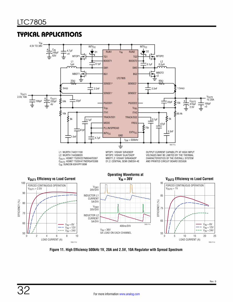
LTC7805
32Rev. 0
For more information www.analog.com
TYPICAL APPLICATIONS
Figure 11. High Efficiency 500kHz 1V, 20A and 2.5V, 10A Regulator with Spread Spectrum
0.1µF
D1 D2
L11µH
MTOP1 MTOP2
1.5mΩ
MBOT2×2
MBOT1
0.1µFL2
0.2µH
100µF
3mΩ
34k
16k
7805 F11a
LTC7805
RUN1 RUN2
SW1
BG1
TG1
BOOST1
SENSE1–
VIN
INTVCC
VIN4.5V TO 38V
VOUT12.5V, 10A VOUT2
1V, 20A
SENSE1+
SENSE2–
TRACK/SS2
ITH2
VFB2
PLLIN/SPREAD
MODE
SENSE2+
SW2
BG2
TG2
BOOST2
VFB1
PGOOD2PGOOD1
INTVCC
ITH1
TRACK/SS1
FREQ
EXTVCCGND
15k
60.4k
0.1µF
3.3nF
5k
47pF
1.5nF
8k 0.1µF
75k
4.7µFfSW = 500kHz
CIN100µF63V
4.7µF×4
+INTVCC
COUT1220µF4V
+
47pF
100µF×3
COUT2470µF2.5V
+
L1: WURTH 744311100L2: WURTH 744308020COUT1: KEMET T520V227M004ATE007COUT2: KEMET T520V477M2R5ATE006CIN: SUNCON 63HVPF100M
MTOP1: VISHAY SIR426DPMTOP2: VISHAY SIJA72ADPMBOT1,2: VISHAY SIR640ADPD1,2: CENTRAL SEMI CMDSH-4E
OUTPUT CURRENT CAPABILITY AT HIGH INPUT VOLTAGES MAY BE LIMITED BY THE THERMALCHARACTERISTICS OF THE OVERALL SYSTEM AND PRINTED CIRCUIT BOARD DESIGN
2.2nF 2.2nF
33Ω 60Ω
22pF 22pF
VOUT1 Efficiency vs Load CurrentOperating Waveforms at
VIN = 36V VOUT2 Efficiency vs Load Current
VOUT1 = 2.5V
VIN = 6VVIN = 12VVIN = 24V
LOAD CURRENT (A)0 2 4 6 8 10
50
60
70
80
90
100
EFFI
CIEN
CY (%
)
7805 F11b
FORCED CONTINUOUS OPERATION
VIN = 36V5A LOAD ON EACH CHANNEL
400ns/DIV
INDUCTOR L2CURRENT
5A/DIV
INDUCTOR L1CURRENT
5A/DIV
VSW220V/DIV
VSW120V/DIV
7805 F11c
VOUT2 = 1V
VIN = 6VVIN = 12VVIN = 24V
LOAD CURRENT (A)0 5 10 15 20 25
55
65
75
85
95
EFFI
CIEN
CY (%
)
7805 F11d
FORCED CONTINUOUS OPERATION
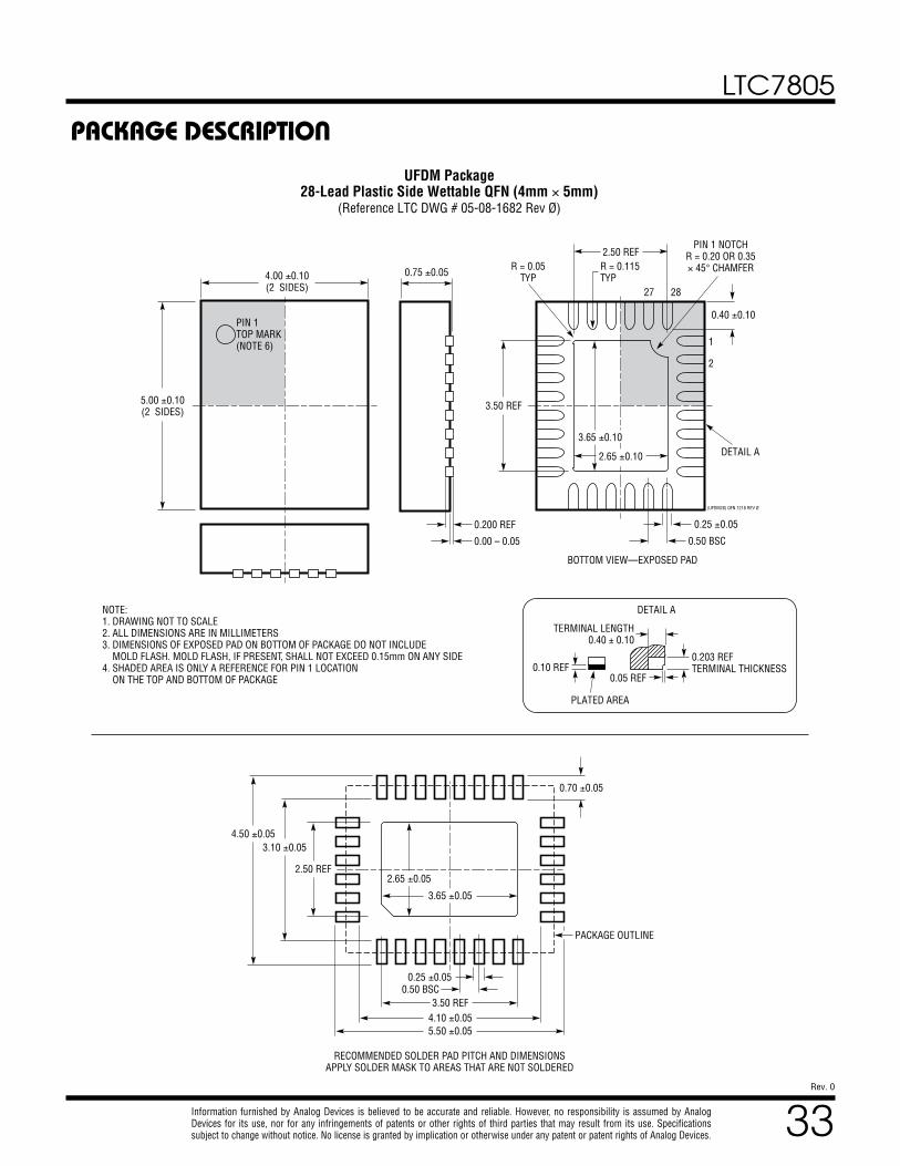
LTC7805
33Rev. 0
For more information www.analog.com
Information furnished by Analog Devices is believed to be accurate and reliable. However, no responsibility is assumed by Analog Devices for its use, nor for any infringements of patents or other rights of third parties that may result from its use. Specifications subject to change without notice. No license is granted by implication or otherwise under any patent or patent rights of Analog Devices.
PACKAGE DESCRIPTION
4.00 ±0.10(2 SIDES)
2.50 REF
5.00 ±0.10(2 SIDES)
NOTE:1. DRAWING NOT TO SCALE2. ALL DIMENSIONS ARE IN MILLIMETERS3. DIMENSIONS OF EXPOSED PAD ON BOTTOM OF PACKAGE DO NOT INCLUDE MOLD FLASH. MOLD FLASH, IF PRESENT, SHALL NOT EXCEED 0.15mm ON ANY SIDE4. SHADED AREA IS ONLY A REFERENCE FOR PIN 1 LOCATION ON THE TOP AND BOTTOM OF PACKAGE
PIN 1TOP MARK(NOTE 6)
0.40 ±0.10
27 28
1
2
BOTTOM VIEW—EXPOSED PAD
3.50 REF
0.75 ±0.05 R = 0.115TYP
R = 0.05TYP
PIN 1 NOTCHR = 0.20 OR 0.35× 45° CHAMFER
0.25 ±0.05
0.50 BSC
0.200 REF
0.00 – 0.05
(UFDM28) QFN 1218 REV Ø
RECOMMENDED SOLDER PAD PITCH AND DIMENSIONSAPPLY SOLDER MASK TO AREAS THAT ARE NOT SOLDERED
0.70 ±0.05
0.25 ±0.050.50 BSC
2.50 REF
3.50 REF4.10 ±0.055.50 ±0.05
2.65 ±0.05
3.10 ±0.054.50 ±0.05
PACKAGE OUTLINE
2.65 ±0.10
3.65 ±0.10
3.65 ±0.05
UFDM Package28-Lead Plastic Side Wettable QFN (4mm × 5mm)
(Reference LTC DWG # 05-08-1682 Rev Ø)
0.203 REFTERMINAL THICKNESS
TERMINAL LENGTH0.40 ± 0.10
0.05 REF
PLATED AREA
DETAIL A
0.10 REF
DETAIL A

LTC7805
34Rev. 0
For more information www.analog.com ANALOG DEVICES, INC. 2021
07/21www.analog.com
RELATED PARTS
TYPICAL APPLICATION
Figure 12. High Efficiency 360W 2-Phase Single Output 12V Step-Down Regulator
D1
MTOP1
2mΩ
MBOT1
0.1µF
1nF
1nF
L1, 4.7µH
7805 F12a
LTC7805
RUN1
RUN2
VFB2
MODE
INTVCC
INTVCC
VIN
VIN16V TO 38V
VOUT12V, 30A
SENSE1–
BOOST2
EXTVCC
VFB1
TG2
SW2
BG2
ITH1
TRACK/SS1
PGOOD1
PGOOD2
ITH2
TRACK/SS2
FREQ
PLLIN/SPREAD
SENSE1+
SW1
BG1
TG1BOOST1
GND
140k
10k
0.1µF
100pF
10nF
5.9k
185k
2mΩ
SENSE2+
SENSE2–
100µF 10µF+
INTVCC
VIN
D2
MTOP2
MBOT2
0.1µF L2, 4.7µH
INTVCC
VIN
COUT330µF16V
10µF×610pF
+
4.7µF
fSW = 200kHzMTOP1,2: VISHAY SIJA72ADPMBOT1,2: VISHAY SIR640ADPL1,2: COILCRAFT XAL1510-472MEBD1,2: CENTRAL SEMI CMDSH-4ECOUT: KEMET T521X337M016ATE025
PART NUMBER DESCRIPTION COMMENTS
LTC7802/LTC7802-3.3
40V Dual Low IQ, 2-Phase Synchronous Step-Down DC/DC Controller with Spread Spectrum, -3.3 Version has fixed 3.3VOUT1
4.5V ≤ VIN ≤ 40V, VOUT Up to 40V, IQ = 12µA, PLL Fixed Frequency 100kHz to 3MHz, Side Wettable 4mm × 5mm QFN-28
LTC7803/LTC7803-3.3
40V Low IQ, Synchronous Step-Down DC/DC Controller with Spread Spectrum and 100% Duty Cycle Capability, -3.3 Version Has Fixed 3.3VOUT
4.5V ≤ VIN ≤ 40V, VOUT Up to 40V, IQ = 12µA, PLL Fixed Frequency 100kHz to 3MHz, 3mm × 3mm QFN-16/MSOP-16
LTC7819 40V Low IQ, Triple Output, 3-Phase Synchronous Step-Down DC/DC Controller
4.5V ≤ VIN ≤ 40V, 0.8V ≤ VOUT ≤ 0.99VIN, IQ = 14µA, PLL Fixed Frequency 100kHz to 3MHz, 6mm × 6mm QFN-40
LTC7804 40V Low IQ, Synchronous Boost Controller with Spread Spectrum and 100% Duty Cycle Capability
4.5V ≤ VIN ≤ 40V, VOUT Up to 40V, 100kHZ to 3MHz Fixed Operating Frequency, 3mm × 3mm QFN-16/MSOP-16
LTC7806 40V, Low IQ, 2-Phase Synchronous Boost DC/DC Controller with Spread Spectrum and 100% Duty Cycle Capability
4.5V ≤ VIN ≤ 40V, VOUT Up to 40V, 100kHZ to 3MHz Fixed Operating Frequency, Side Wettable 4mm × 5mm QFN-28
LTC3890/LTC3890-1/LTC3890-2/LTC3890-3
60V, Low IQ, Dual 2-Phase Synchronous Step-Down DC/DC Controller
4V ≤ VIN ≤ 60V, 0.8V ≤ VOUT ≤ 24V, IQ = 50µA, PLL Fixed Frequency 50kHz to 900kHz, 5mm × 5mm QFN-32
LTC3892/LTC3892-1/LTC3892-2
60V Low IQ, Dual, 2-Phase Synchronous Step-Down DC/DC Controller with Adjustable 5V to 10V Gate Drive Voltage
4V ≤ VIN ≤ 60V, 0.8V ≤ VOUT ≤ 24V, IQ = 29µA, PLL Fixed Frequency 50kHz to 900kHz, 5mm × 5mm QFN-32/TSSOP-28
LTC3855 38V Dual, 2-Phase, Synchronous Step-Down DC/DC Controller with Remote Output Voltage Sense
4.5V≤ VIN ≤ 38V, 0.8V ≤ VOUT ≤ 12V, PLL Fixed Frequency 250kHz to 770kHz, 6mm × 6mm QFN-40/TSSOP-40


![Fonte estabilizada [0-40V x 5A].pdf](https://img.pdfslide.net/doc/110x75/577c77441a28abe0548b6581/fonte-estabilizada-0-40v-x-5apdf.jpg)