Embed Size (px)
Citation preview
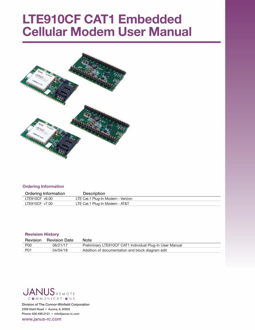
LTE910CF CAT1 Embedded Cellular Modem User Manual
Bulletin JA03-UM-LTE-Cat1Revision P02Date 19 Nov 2019
LTE910CF Plug-In Hardware User Manual JA03-UM-LTE-Cat1 Page 2 Rev: P02 Date: 11/19/19© Copyright 2019 Janus Remote Communications Specifications subject to change without notice
All Rights Reserved See website for latest revision. Not intended for life support applications.
TABLE OF CONTENTSTABLE OF CONTENTS and DISCLAIMER .............................................................................................................................. 21 APPLICABILITY TABLE ........................................................................................................................................................ 32 REFERENCES ...................................................................................................................................................................... 3 2.1 Janus Document List ............................................................................................................................................... 3 2.2 Telit Document List .................................................................................................................................................. 33 OVERVIEW ........................................................................................................................................................................4-6 3.1 Introduction ............................................................................................................................................................. 4 3.2 Preview .................................................................................................................................................................... 4 3.3 LTE Features ............................................................................................................................................................ 5 3.4 LTE Block Diagram .................................................................................................................................................. 5 3.5 FOTA Notice ............................................................................................................................................................ 64 INTERFACES ...................................................................................................................................................................6-15 4.1 Inerface Voltage Selection ....................................................................................................................................... 6 4.2 Serial Interface......................................................................................................................................................7-8 4.3 Power Supply .......................................................................................................................................................... 9 4.4 Audio Interface ........................................................................................................................................................ 9 4.5 Plug-In Pin-Out ...................................................................................................................................................... 10 4.6 VRTC Details ......................................................................................................................................................... 11 4.7 GPIO Details .......................................................................................................................................................... 12 4.8 Analog to Digital Converter ................................................................................................................................... 13 4.9 LED Status Indicators .......................................................................................................................................13-14 4.10 RF Interface ........................................................................................................................................................... 15 4.11 SIM Card Interface ................................................................................................................................................ 15 4.12 Header Interface Mounting Options ...................................................................................................................... 15 4.13 Screw Mounting .................................................................................................................................................... 155 LTE910CF TECHNICAL SPECIFICATIONS ...................................................................................................................16-23 5.1 Electrical Specifications ...................................................................................................................................16-19 5.2 Mechanical Specifications..................................................................................................................................... 206 OPERATIONS ................................................................................................................................................................21-24 6.1 Powering ON/OFF ................................................................................................................................................. 21 6.2 Communicating with the modem .......................................................................................................................... 21 6.3 Testing Communications ....................................................................................................................................... 21 6.4 Cellular Network Communications ........................................................................................................................ 22 6.5 Data Communications ........................................................................................................................................... 23 6.6 SMS ....................................................................................................................................................................... 247 DESIGN CONSIDERATIONS .............................................................................................................................................. 25 7.1 Minimum Required Module Pin Connects............................................................................................................. 25 7.2 Debug .................................................................................................................................................................... 25
APPENDICES ........................................................................................................................................................................ 25 Approvals .............................................................................................................................................................. 25 Safety .................................................................................................................................................................... 25 Antenna Care and Replacement ........................................................................................................................... 25 Abbreviations ......................................................................................................................................................... 25 Ordering Information ............................................................................................................................................. 26 Revision History..................................................................................................................................................... 26
DISCLAIMERThe information contained in this document is the proprietary information of Connor-Winfield Corporation and its affiliates (Janus Remote Communication). The contents are confidential and any disclosure to persons other than the officers, employees, agents or subcontractors of the owner or licensee of this document, without the prior written consent of Connor-Winfield, is strictly prohibited. Connor-Winfield makes every effort to ensure the quality of the information it makes available. Notwithstanding the foregoing, Connor-Winfield does not make any warranty as to the information contained herein, and does not accept any liability for any injury, loss or damage of any kind incurred by use of or reliance upon the information. Connor-Winfield disclaims any and all responsibility for the application of the devices characterized in this document, and notes that the application of the device must comply with the safety standards of the applicable country, and where applicable, with the relevant wiring rules. Connor-Winfield reserves the right to make modifications, additions and deletions to this document due to typographical errors, inaccurate information, or improvements to programs and/or equipment at any time and without notice. Such changes will, nevertheless be incorporated into new editions of this application note.
All rights reserved 2019 Connor-Winfield Corporation
LTE910CF Plug-In Hardware User Manual JA03-UM-LTE-Cat1 Page 3 Rev: P02 Date: 11/19/19© Copyright 2019 Janus Remote Communications Specifications subject to change without notice
All Rights Reserved See website for latest revision. Not intended for life support applications.
1 APPLICABILITY TABLEProduct Part NumberLTE910CF v6.00LTE910CF v7.00
2 REFERENCES
2.1 Janus Document List
Janus Application Note 117 - FOTA (Firmware Over The Air)
2.2 Telit Document List
Our modem uses Telit LE910-NA1 cellular module. Please refer to Telit’s website at www.telit.com for the latest information on the LE910 V2 module family.
Telit LE910 V2 AT Commands Reference GuideTelit LE910 V2 Hardware User GuideTelit IP Easy User GuideTelit 3G-4G Digital Voice Interface Application Note
LTE910CF Plug-In Hardware User Manual JA03-UM-LTE-Cat1 Page 4 Rev: P02 Date: 11/19/19© Copyright 2019 Janus Remote Communications Specifications subject to change without notice
All Rights Reserved See website for latest revision. Not intended for life support applications.
3 OVERVIEW3.1 Introduction
The User Manual for the Plug-In Modem devices is intended to illustrate how users can integrate and implement the features of each communication version of the device. The common factors are explained in detail, as well as special considerations and diagrams for each module. The module differences are highlighted in this manual for design considerations for future model placement.
3.2 Preview
The Plug-In Modems are self-contained, multi-band, globally capable, M2M communication devices designed to provide a comprehensive solution to application problems for our M2M customers. They utilize the proven technology of Telit’s certified modules for their core communications engines.
3.2.1 Functional Description
Cellular• LTE (V6.00)• LTE/HSPA/UMTS (V7.00)
UART• 115200 bps supporting all 7 standard RS232 signals
USB• HS/FS USB 2.0 Device (480Mb/s)
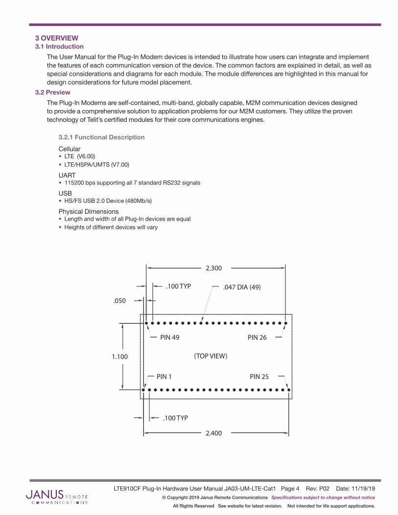
Physical Dimensions• Length and width of all Plug-In devices are equal• Heights of different devices will vary
(TOP VIEW)
.047 DIA (49)
.100 TYP
1.100
.100 TYP
.050
2.400
2.300
PIN 1 PIN 25
PIN 26PIN 49
LTE910CF Plug-In Hardware User Manual JA03-UM-LTE-Cat1 Page 5 Rev: P02 Date: 11/19/19© Copyright 2019 Janus Remote Communications Specifications subject to change without notice
All Rights Reserved See website for latest revision. Not intended for life support applications.
LTE910CF v7.00 (AT&T)• Multi-Band Support
LTE Band 1900 (B2), 1700 (B4), 850 (B5), 700 (B12/B13)UMTS/HSPA+ Band 850 (B5), 1900 (B2)
• Output PowerClass 3 (0.2W) @ LTEClass 3 (0.25W) @ WCDMA
• DataLTE: DL: Up to 10Mbps, UL: Up to 5MbpsHSPA: DL: Up to 42Mbps, UL: Up to 5.76 MbpsUMTS: DL: Up to 384Kbps, UL: Up to 384Kbps
LTE910CF v6.00 (Verizon)• Tri-Band Support
LTE Band 1900 (B2), 1700 (B4), 700 (B13)
• Output Power
Class 3 (0.2W, 23dBm) @ LTE
• Data
LTE: DL: Up to 10Mbps, UL: Up to 5Mbps
Features for Both v6.00 & v7.00• Control via standard and extended AT command set• SIM application Tool Kits 3GPP TS 51.014• SIM access profile• IP stack with TCP/UDP protocol support• SMS Support• Through hole for screw mount• Dimensions: 2.5” x 1.4” x 0.325”• Operational Temperature Range: -40°C to 85°C• Internal Switching Regulator:
Input Voltage Range: 4.75 to 5.25Vdc (5Vdc nominal)Supply disable via terminal input pin
• Variable logic level (UART/GPIO)Adjustable from 1.8 - 5.0VdcDefaults to 2.85v
• SIM CardStandard locking SIM card socket
• Cellular, Rx Diversity & MIMO DL 2x2 antenna connec-tions via Hirose U.FL miniature RF connectors
3.4 Block Diagram
3 OVERVIEW continued3.3 Features
Figure 1 LTE910CF CAT1 Block Diagram
TELITLE910
TELITLE910
SIM CARD SIM CARD
Switching RegulatorSwitching Regulator
LTE910CF
GPIO2 : USER LED
USB
VSel UART (AT)
VSel UART (TRACE)
VSel GPIO (3-7)
5 VDC
ENABLE
1.8v PWRMON
RESET
ON/OFF
1.8v VRTC
GPIO1 : Cellular LED
1.8v DVI
LDOLDO 2.85v
TranslatorTranslator1.8v UART (AT)
1.8v UART (TRACE)1.8v PWRMON
VSel PWRMON
1.8v UART (AT)
1.8v UART (TRACE)
1.8v PWRMONEnable
Enable
1.8v GPIO
1.8v GPIO
1.8v GPIO9 / I2C SDA
1.8v GPIO10 / I2C SCL
Reference
VL
2.85vVo
Select
Vo
SelectVSel VAUXVSel
LTE910CF Plug-In Hardware User Manual JA03-UM-LTE-Cat1 Page 6 Rev: P02 Date: 11/19/19© Copyright 2019 Janus Remote Communications Specifications subject to change without notice
All Rights Reserved See website for latest revision. Not intended for life support applications.
3 OVERVIEW continued3.5 FOTA Notice
The LTE910CF is equipped with a variable voltage interface solution. This allows the user to match the device to the system’s level without extra hardware. Once a voltage has been injected, the unit will swap to the chosen voltage immediately for the affected I/O.
The VL_IN signal can be applied or changed to a different level within the 1.5V to 5.5V operational range after the unit is powered, but once applied the VL_IN voltage should not be removed unless the unit is turned off.
If no external reverence is applied to the VL_IN pin, the I/O interface will default to a 2.85V level. In this case the VL_IN pin 30 should be pulled low.
Truth Table:VL_IN: Ground 1.5v - 5.5vI/O level: 2.85v 1.5v - 5.5v
Affected I/O:
1. UART (AT, TRACE)
2. GPIO (3-7)
3. VAUX
VAUX Adjustment allows feedback as well as legacy access if previously utilizing a plug in implementation with VAUX as the reference.
Note to pay attention of these changes so there are no adverse effects on a previous Plug in Modem implementation.
The certification of LTE devices for use on the Verizon Wireless network REQUIRES that the end user implement an automated FOTA procedure on their devices that would allow the cellular module firmware to be updated if required. Failure to implement an automated FOTA procedure violates the certification requirements of the cellular modem and may result in units becoming unusable on the cellular network in the future. Your end device must support the firmware over the air update for the cellular modem You may use your own FOTA system to update the cellular modem firmware over the air. You may also be able to use the Verizon Wireless FOTA system, and FOTA services may be available from other 3rd party vendors. To inquire about Verizon Wireless FOTA system information and technical specifications, contact [email protected]
4 INTERFACES4.1 Interface Voltage Selection
LTE910CF Plug-In Hardware User Manual JA03-UM-LTE-Cat1 Page 7 Rev: P02 Date: 11/19/19© Copyright 2019 Janus Remote Communications Specifications subject to change without notice
All Rights Reserved See website for latest revision. Not intended for life support applications.
4 INTERFACES4.2 Serial Interface
4.2.1 UART Serial Port
The serial interface is a CMOS level UART. Default Communications settings for this port are as follows:• Baud Rate: 115.2 kbps• Bits: 8• Stop Bits: 1• Parity: None• Hardware Handshaking: Yes
Baud rate can be controlled with the AT+IPR command. Default setting is 115200 baud. Note: If you are not using hardware handshaking, RTS must be connected to GROUND for proper communications when flow control is not used.
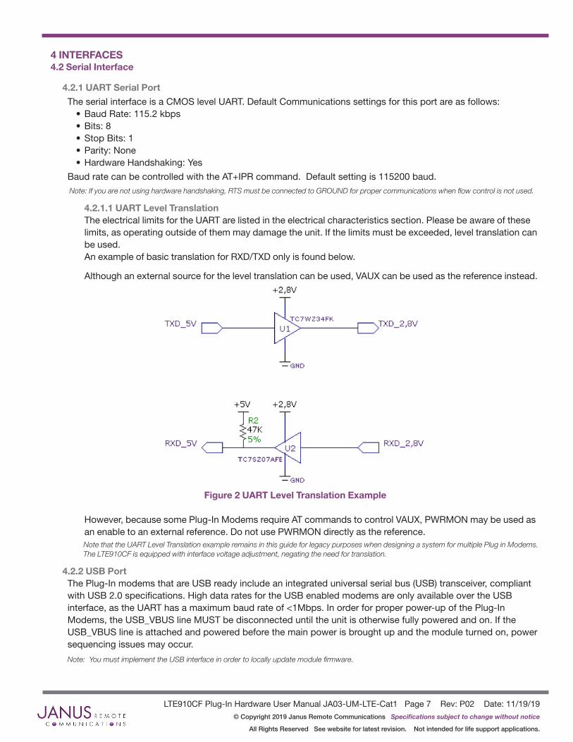
4.2.1.1 UART Level TranslationThe electrical limits for the UART are listed in the electrical characteristics section. Please be aware of these limits, as operating outside of them may damage the unit. If the limits must be exceeded, level translation can be used. An example of basic translation for RXD/TXD only is found below.
Although an external source for the level translation can be used, VAUX can be used as the reference instead.
However, because some Plug-In Modems require AT commands to control VAUX, PWRMON may be used as an enable to an external reference. Do not use PWRMON directly as the reference.Note that the UART Level Translation example remains in this guide for legacy purposes when designing a system for multiple Plug in Modems. The LTE910CF is equipped with interface voltage adjustment, negating the need for translation.
4.2.2 USB PortThe Plug-In modems that are USB ready include an integrated universal serial bus (USB) transceiver, compliant with USB 2.0 specifications. High data rates for the USB enabled modems are only available over the USB interface, as the UART has a maximum baud rate of <1Mbps. In order for proper power-up of the Plug-In Modems, the USB_VBUS line MUST be disconnected until the unit is otherwise fully powered and on. If the USB_VBUS line is attached and powered before the main power is brought up and the module turned on, power sequencing issues may occur.
Note: You must implement the USB interface in order to locally update module firmware.
Figure 2 UART Level Translation Example
LTE910CF Plug-In Hardware User Manual JA03-UM-LTE-Cat1 Page 8 Rev: P02 Date: 11/19/19© Copyright 2019 Janus Remote Communications Specifications subject to change without notice
All Rights Reserved See website for latest revision. Not intended for life support applications.
Figure 3 USB Connection Diagram
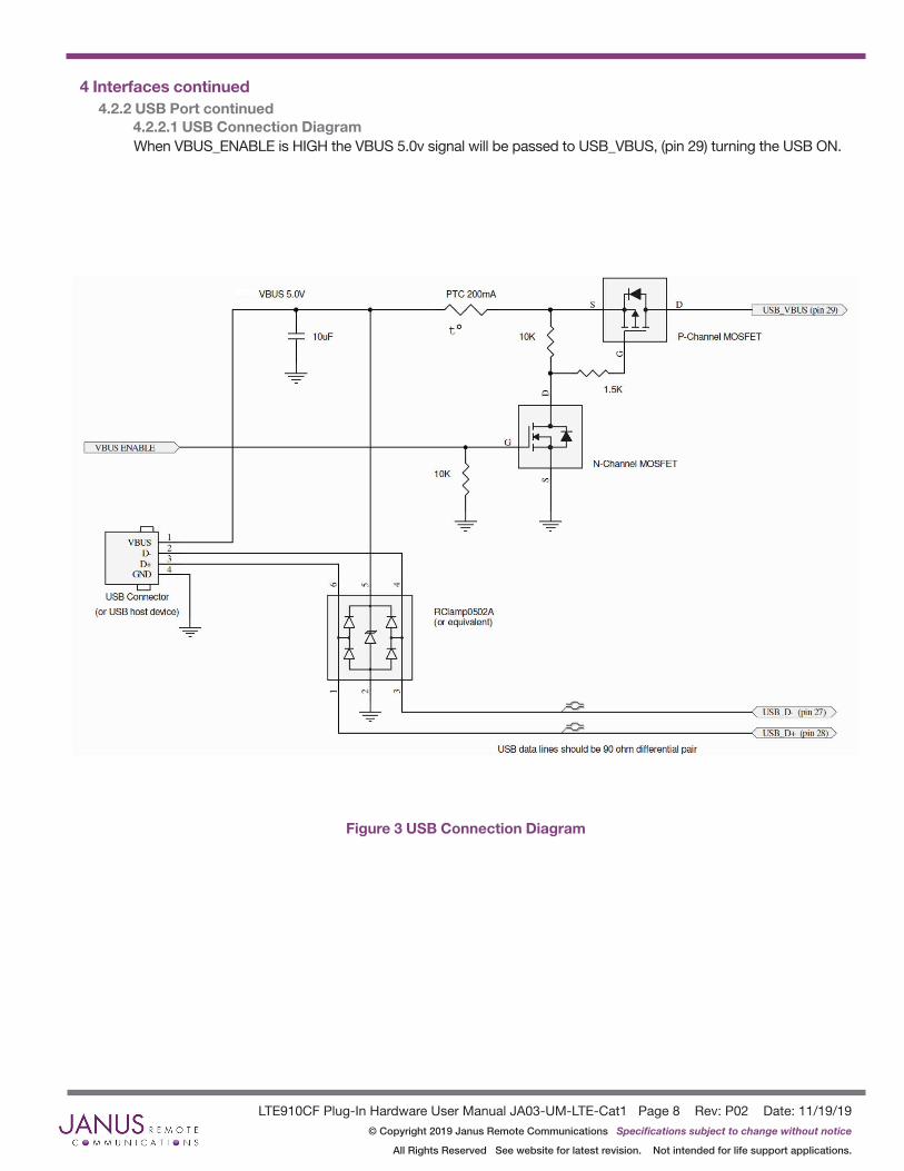
4 Interfaces continued4.2.2 USB Port continued 4.2.2.1 USB Connection Diagram
When VBUS_ENABLE is HIGH the VBUS 5.0v signal will be passed to USB_VBUS, (pin 29) turning the USB ON.
LTE910CF Plug-In Hardware User Manual JA03-UM-LTE-Cat1 Page 9 Rev: P02 Date: 11/19/19© Copyright 2019 Janus Remote Communications Specifications subject to change without notice
All Rights Reserved See website for latest revision. Not intended for life support applications.
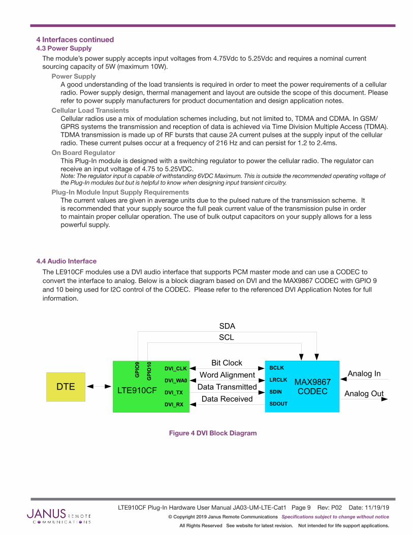
Figure 4 DVI Block Diagram
4.4 Audio Interface
The LE910CF modules use a DVI audio interface that supports PCM master mode and can use a CODEC to convert the interface to analog. Below is a block diagram based on DVI and the MAX9867 CODEC with GPIO 9 and 10 being used for I2C control of the CODEC. Please refer to the referenced DVI Application Notes for full information.
4 Interfaces continued4.3 Power Supply
The module’s power supply accepts input voltages from 4.75Vdc to 5.25Vdc and requires a nominal current sourcing capacity of 5W (maximum 10W).
Power SupplyA good understanding of the load transients is required in order to meet the power requirements of a cellular radio. Power supply design, thermal management and layout are outside the scope of this document. Please refer to power supply manufacturers for product documentation and design application notes.
Cellular Load TransientsCellular radios use a mix of modulation schemes including, but not limited to, TDMA and CDMA. In GSM/GPRS systems the transmission and reception of data is achieved via Time Division Multiple Access (TDMA). TDMA transmission is made up of RF bursts that cause 2A current pulses at the supply input of the cellular radio. These current pulses occur at a frequency of 216 Hz and can persist for 1.2 to 2.4ms.
On Board RegulatorThis Plug-In module is designed with a switching regulator to power the cellular radio. The regulator can receive an input voltage of 4.75 to 5.25VDC.Note: The regulator input is capable of withstanding 6VDC Maximum. This is outside the recommended operating voltage of the Plug-In modules but but is helpful to know when designing input transient circuitry.
Plug-In Module Input Supply Requirements The current values are given in average units due to the pulsed nature of the transmission scheme. It is recommended that your supply source the full peak current value of the transmission pulse in order to maintain proper cellular operation. The use of bulk output capacitors on your supply allows for a less powerful supply.
LTE910CF DTE MAX9867 CODEC
Bit Clock
Word Alignment
Data Transmitted
Data Received
SDA
SCL
G
PIO
9
GP
IO10
Analog Out
Analog InDVI_CLK
DVI_WA0
DVI_TX
DVI_RX
BCLK
LRCLK
SDIN
SDOUT
LTE910CF Plug-In Hardware User Manual JA03-UM-LTE-Cat1 Page 10 Rev: P02 Date: 11/19/19© Copyright 2019 Janus Remote Communications Specifications subject to change without notice
All Rights Reserved See website for latest revision. Not intended for life support applications.
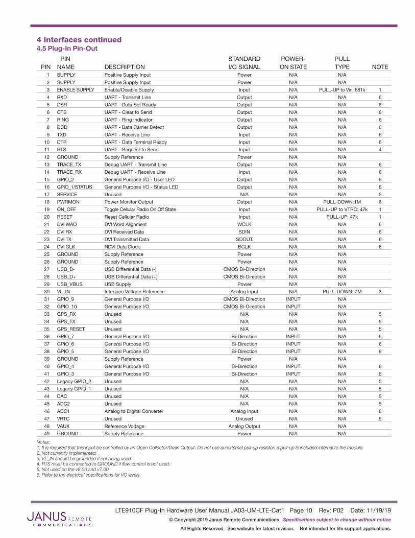
4 Interfaces continued4.5 Plug-In Pin-Out
PIN STANDARD POWER- PULL PIN NAME DESCRIPTION I/O SIGNAL ON STATE TYPE NOTE 1 SUPPLY Positive Supply Input Power N/A N/A
2 SUPPLY Positive Supply Input Power N/A N/A
3 ENABLE SUPPLY Enable/Disable Supply Input N/A PULL-UP to Vin: 681k 1
4 RXD UART - Transmit Line Output N/A N/A 6
5 DSR UART - Data Set Ready Output N/A N/A 6
6 CTS UART - Clear to Send Output N/A N/A 6
7 RING UART - Ring Indicator Output N/A N/A 6
8 DCD UART - Data Carrier Detect Output N/A N/A 6
9 TXD UART - Receive Line Input N/A N/A 6
10 DTR UART - Data Terminal Ready Input N/A N/A 6
11 RTS UART - Request to Send Input N/A N/A 4
12 GROUND Supply Reference Power N/A N/A
13 TRACE_TX Debug UART - Transmit Line Output N/A N/A 6
14 TRACE_RX Debug UART - Receive Line Input N/A N/A 6
15 GPIO_2 General Purpose I/O - User LED Output N/A N/A 6
16 GPIO_1/STATUS General Purpose I/O - Status LED Output N/A N/A 6
17 SERVICE Unused N/A N/A N/A 5
18 PWRMON Power Monitor Output Output N/A PULL-DOWN:1M 6
19 ON_OFF Toggle Cellular Radio On Off State Input N/A PULL-UP to VTRC: 47k 1
20 RESET Reset Cellular Radio Input N/A PULL-UP: 47k 1
21 DVI WAO DVI Word Alignment WCLK N/A N/A 6
22 DVI RX DVI Received Data SDIN N/A N/A 6
23 DVI TX DVI Transmitted Data SDOUT N/A N/A 6
24 DVI CLK NDVI Data Clock BCLK N/A N/A 6
25 GROUND Supply Reference Power N/A N/A
26 GROUND Supply Reference Power N/A N/A
27 USB_D- USB Differential Data (-) CMOS Bi-Direction N/A N/A
28 USB_D+ USB Differential Data (+) CMOS Bi-Direction N/A N/A
29 USB_VBUS USB Supply Power N/A N/A
30 VL_IN Interface Voltage Reference Analog Input N/A PULL-DOWN: 7M 3
31 GPIO_9 General Purpose I/O CMOS Bi-Direction INPUT N/A
32 GPIO_10 General Purpose I/O CMOS Bi-Direction INPUT N/A
33 GPS_RX Unused N/A N/A N/A 5
34 GPS_TX Unused N/A N/A N/A 5
35 GPS_RESET Unused N/A N/A N/A 5
36 GPIO_7 General Purpose I/O Bi-Direction INPUT N/A 6
37 GPIO_6 General Purpose I/O Bi-Direction INPUT N/A 6
38 GPIO_5 General Purpose I/O Bi-Direction INPUT N/A 6
39 GROUND Supply Reference Power N/A N/A
40 GPIO_4 General Purpose I/O Bi-Direction INPUT N/A 6
41 GPIO_3 General Purpose I/O Bi-Direction INPUT N/A 6
42 Legacy GPIO_2 Unused N/A N/A N/A 5
43 Legacy GPIO_1 Unused N/A N/A N/A 5
44 DAC Unused N/A N/A N/A 5
45 ADC2 Unused N/A N/A N/A 5
46 ADC1 Analog to Digital Converter Analog Input N/A N/A 6
47 VRTC Unused Unused N/A N/A 5
48 VAUX Reference Voltage Analog Output N/A N/A
49 GROUND Supply Reference Power N/A N/A
Notes: 1. It is required that this input be controlled by an Open Collector/Drain Output. Do not use an external pull-up resistor; a pull-up is included internal to the module. 2. Not currently implemented. 3. VL_IN should be grounded if not being used. 4. RTS must be connected to GROUND if flow control is not used. 5. Not used on the v6.00 and v7.00. 6. Refer to the electrical specifications for I/O levels.
LTE910CF Plug-In Hardware User Manual JA03-UM-LTE-Cat1 Page 11 Rev: P02 Date: 11/19/19© Copyright 2019 Janus Remote Communications Specifications subject to change without notice
All Rights Reserved See website for latest revision. Not intended for life support applications.
4 Interfaces continued4.6 VRTC Details
The VRTC pin brings out the real time clock supply, which is separate from the rest of the part. This allows only the RTC to be ON when all other parts of the device are OFF. A backup capacitor can be added to this pin to increase RTC autonomy while powering the device from a battery.
No devices should be powered from this pin.
Equations:C = 3600 * [(Btime * IRTC)/(VRTC - VRTCmin)]Btime = [C * (VRTC - VRTCmin)/(IRTC * 3600)]
Where:VRTC – The Starting voltage of the capacitor (Volt)VRTCmin – The minimum voltage acceptable for the RTC circuit. (Volt)IRTC – The current consumption of the RTC circuitry when VBATT = 0 (Ampere) Btime - Backup Time (Hours)C = Capacitor value (Farads)
Values for the LTE910CFVRTC = 1.8v NominalVRTC minimum input voltage to function = 1.1vIRTC = 2uA nominal
For Example,Btime = 96 hours (4 days)C = 1.0F
LTE910CF Plug-In Hardware User Manual JA03-UM-LTE-Cat1 Page 12 Rev: P02 Date: 11/19/19© Copyright 2019 Janus Remote Communications Specifications subject to change without notice
All Rights Reserved See website for latest revision. Not intended for life support applications.
4 Interfaces continued4.7 GPIO Details
GPIO are configurable as input, output, and alternate function. Configuration is controlled by AT commands. Alternate functions include cellular status, ALARM pin function, temperature monitor indication and DAC output.
4.7.1 Using a GPIO Pad as INPUTThe GPIO pads, when used as inputs, can be connected to a digital output of another device and report its status, provided this device has interface levels compatible with the Voltage levels of the GPIO of the module.
4.7.2 Using a GPIO Pad as OUTPUTThe GPIO pads, when used as outputs, can drive CMOS digital devices or compatible hardware. When set as outputs, the pads have a push-pull output.
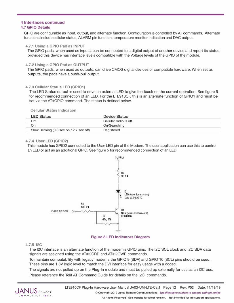
4.7.3 Cellular Status LED (GPIO1)The LED Status output is used to drive an external LED to give feedback on the current operation. See figure 5 for recommended connection of an LED. For the LTE910CF, this is an alternate function of GPIO1 and must be set via the AT#GPIO command. The status is defined below.
Cellular Status Indication
LED Status Device StatusOff Cellular radio is offOn On/SearchingSlow Blinking (0.3 sec on / 2.7 sec off) Registered
4.7.4 User LED (GPIO2)This module has GPIO2 connected to the User LED pin of the Modem. The user application can use this to control an LED or act as an additional GPIO. See figure 5 for recommended connection of an LED.
Figure 5 LED Indicators Diagram
4.7.5 I2CThe I2C interface is an alternate function of the modem’s GPIO pins. The I2C SCL clock and I2C SDA data signals are assigned using the AT#I2CRD and AT#I2CWR commands.To maintain compatability with legacy modems the GPIO 9 (SDA) and GPIO 10 (SCL) pins should be used. These pins are 1.8V logic level to match the DVI interface for easy usage with a codec. The signals are not pulled up on the Plug-In module and must be pulled up externally for use as an I2C bus.Please reference the Telit AT Command Guide for details on the I2C commands.
LTE910CF Plug-In Hardware User Manual JA03-UM-LTE-Cat1 Page 13 Rev: P02 Date: 11/19/19© Copyright 2019 Janus Remote Communications Specifications subject to change without notice
All Rights Reserved See website for latest revision. Not intended for life support applications.
4 Interfaces continued4.8 Analog to Digital Converter
Pin 46 is connected directly to the Telit module ADC pin. It has a 0 to 1.2V range with 10 bit resolution. Use the command AT#ADC=1.2<cr> to read the ADC. The returned value is expressed in millivolts.
ADC Description ADC1 Analog to digital converted input
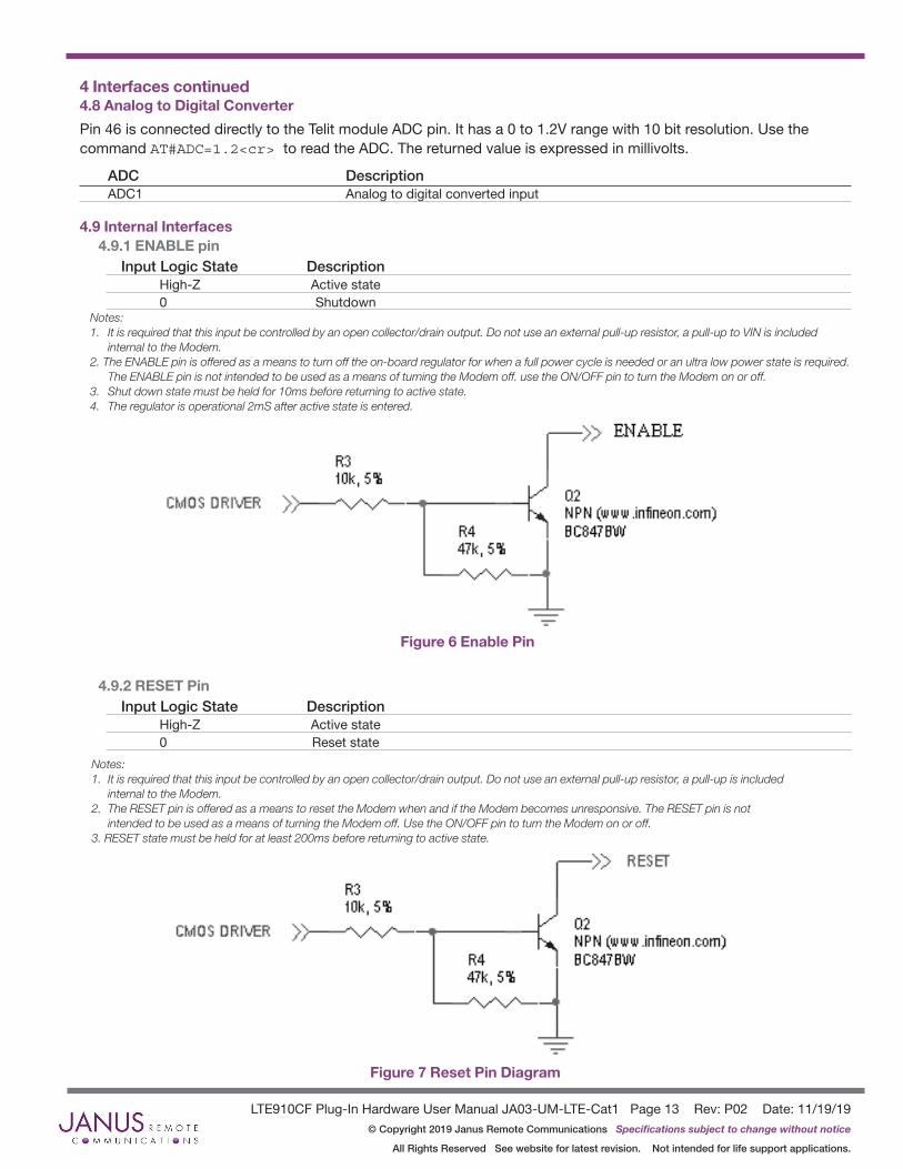
4.9 Internal Interfaces4.9.1 ENABLE pin
Input Logic State Description High-Z Active state 0 Shutdown Notes:1. It is required that this input be controlled by an open collector/drain output. Do not use an external pull-up resistor, a pull-up to VIN is included internal to the Modem.2. The ENABLE pin is offered as a means to turn off the on-board regulator for when a full power cycle is needed or an ultra low power state is required. The ENABLE pin is not intended to be used as a means of turning the Modem off. use the ON/OFF pin to turn the Modem on or off.3. Shut down state must be held for 10ms before returning to active state. 4. The regulator is operational 2mS after active state is entered.
4.9.2 RESET Pin Input Logic State Description High-Z Active state 0 Reset state
Notes: 1. It is required that this input be controlled by an open collector/drain output. Do not use an external pull-up resistor, a pull-up is included internal to the Modem. 2. The RESET pin is offered as a means to reset the Modem when and if the Modem becomes unresponsive. The RESET pin is not intended to be used as a means of turning the Modem off. Use the ON/OFF pin to turn the Modem on or off. 3. RESET state must be held for at least 200ms before returning to active state.
Figure 7 Reset Pin Diagram
Figure 6 Enable Pin
LTE910CF Plug-In Hardware User Manual JA03-UM-LTE-Cat1 Page 14 Rev: P02 Date: 11/19/19© Copyright 2019 Janus Remote Communications Specifications subject to change without notice
All Rights Reserved See website for latest revision. Not intended for life support applications.
4 Interfaces continued4.9 GPIO Details continued
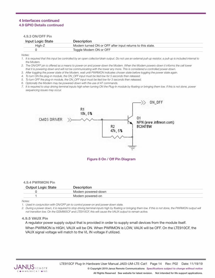
4.9.3 ON/OFF Pin Input Logic State Description High-Z Modem turned ON or OFF after input returns to this state. 0 Toggle Modem ON or OFF
Notes: 1. It is required that this input be controlled by an open collector/drain output. Do not use an external pull-up resistor, a pull-up is included internal to the Modem. 2. The ON/OFF pin is offered as a means to power-on and power-down the Modem. When the Modem powers-down it informs the cell tower that it is powering down and will not be communicating with the tower any more. This is considered a controlled power-down. 3. After toggling the power state of the Modem, wait until PWRMON indicates chosen state before toggling the power state again. 4. To turn ON the plug-in module, the ON_OFF input must be tied low for 5 seconds then released.5. To turn OFF the plug-in module, the ON_OFF input must be tied low for 3 seconds then released.6. Optionally the Modem may be powered-down with the use of AT commands. 7. It is required to stop driving terminal inputs high when turning ON the Plug-In module by floating or bringing them low. If this is not done, power sequencing issues may occur.
4.9.4 PWRMON Pin Output Logic State Description 0 Modem powered-down 1 Modem powered-on
Notes: 1. Used in conjunction with ON/OFF pin to control power-on and power-down state.2. During a power down, it is required to stop driving terminal inputs high by floating or bringing them low. If this is not done, the PWRMON output will not transition low. On the GSM865CF and LTE910CF, this will cause the VAUX output to remain active.
4.9.5 VAUX PinA regulator power supply output that is provided in order to supply small devices from the module itself.
When PWRMON is HIGH, VAUX will be ON. When PWRMON is LOW, VAUX will be OFF. On the LTE910CF, the VAUX signal voltage will match to the VL IN voltage if utilized.
Figure 8 On / Off Pin Diagram
LTE910CF Plug-In Hardware User Manual JA03-UM-LTE-Cat1 Page 15 Rev: P02 Date: 11/19/19© Copyright 2019 Janus Remote Communications Specifications subject to change without notice
All Rights Reserved See website for latest revision. Not intended for life support applications.
4 Interfaces continued
4.10 RF Interface
There are two RF interfaces on the LTE910CF. A cellular and MIMO/RX diversity connector. The specifications and requirements for these are as follows:4.10.1 LTE910CF Antenna Interface
Type: Hirose U.FL - MALE (Part Number: U.FL-R-SMT(10)
Pin Description Center Pin RF signal Outer Conductor Signal ground
4.11 SIM Card Interface
The SIM Card Interface allows the Modem to accept the subscriber card provided by the cellular telephone provider. It can accommodate a 1.8v or 3.0v SIM card.
4.12 Header Interface Mounting Options
The Plug-In Modules’ header pin length has been chosen to allow for direct solder mount to a PCB of standard thickness. If the user wishes to socket the Plug-In Module, they may do so as well by using the below part numbers for reference:
Samtec 25 pin header: TSM-125-04-L-SV-A
Samtec 24 pin header: TSM-124-04-L-SV-A
Mating Samtec 25 pin connector: SLW-125-01-G-S
Mating Samtec 24 pin connector: SLW-124-01-G-S
Please note there are no Samtec SMT single row mating connectors. The only mating connector available is the above listed THT version.
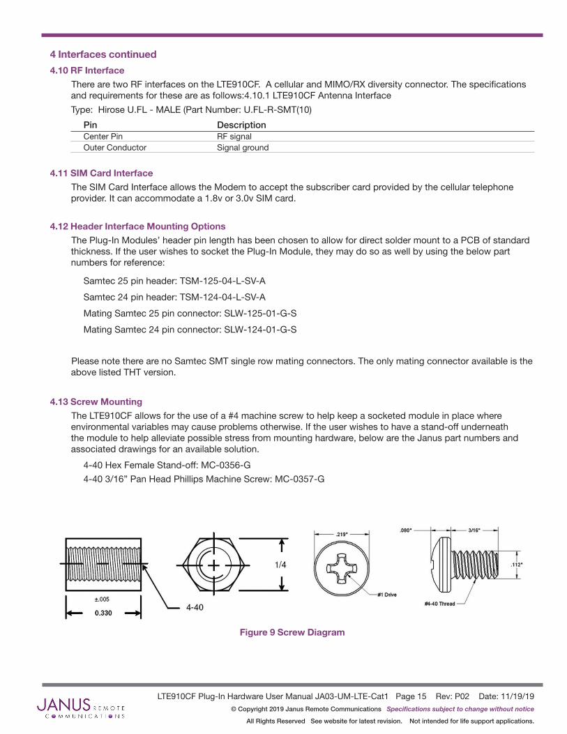
4.13 Screw Mounting
The LTE910CF allows for the use of a #4 machine screw to help keep a socketed module in place where environmental variables may cause problems otherwise. If the user wishes to have a stand-off underneath the module to help alleviate possible stress from mounting hardware, below are the Janus part numbers and associated drawings for an available solution.
4-40 Hex Female Stand-off: MC-0356-G
4-40 3/16” Pan Head Phillips Machine Screw: MC-0357-G
Figure 9 Screw Diagram
LTE910CF Plug-In Hardware User Manual JA03-UM-LTE-Cat1 Page 16 Rev: P02 Date: 11/19/19© Copyright 2019 Janus Remote Communications Specifications subject to change without notice
All Rights Reserved See website for latest revision. Not intended for life support applications.
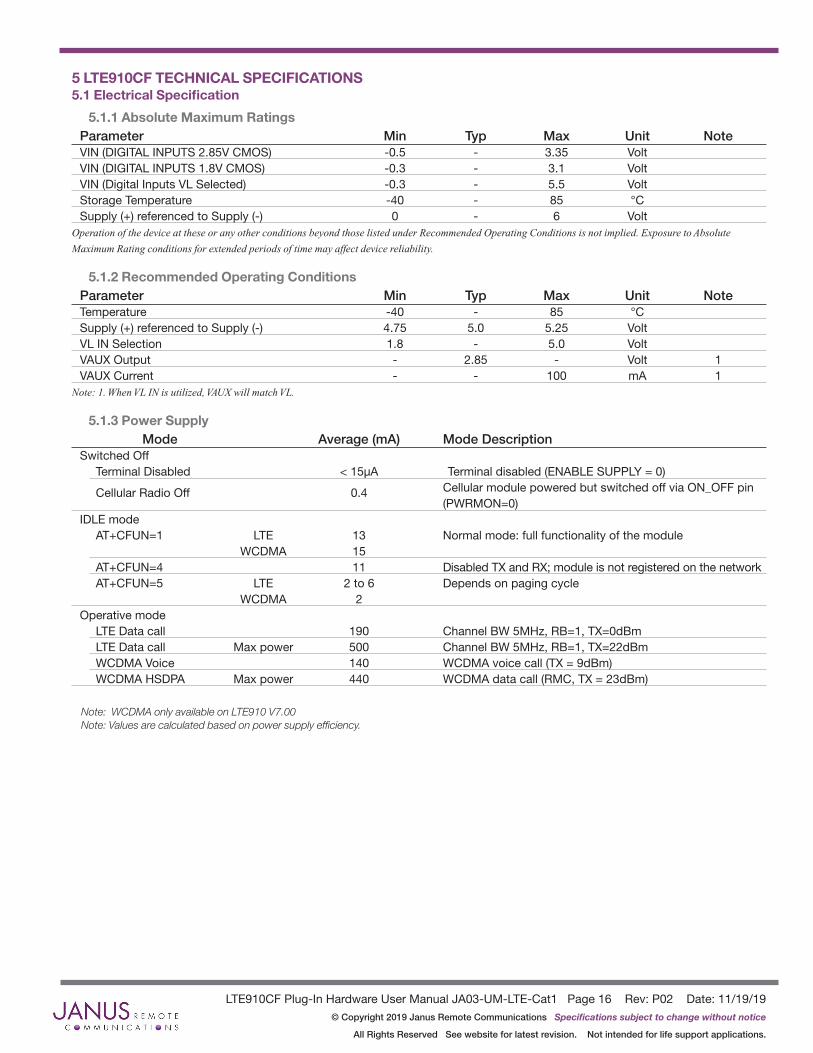
5 LTE910CF TECHNICAL SPECIFICATIONS5.1 Electrical Specification
5.1.1 Absolute Maximum Ratings Parameter Min Typ Max Unit Note VIN (DIGITAL INPUTS 2.85V CMOS) -0.5 - 3.35 Volt VIN (DIGITAL INPUTS 1.8V CMOS) -0.3 - 3.1 VoltVIN (Digital Inputs VL Selected) -0.3 - 5.5 VoltStorage Temperature -40 - 85 °C Supply (+) referenced to Supply (-) 0 - 6 Volt
Operation of the device at these or any other conditions beyond those listed under Recommended Operating Conditions is not implied. Exposure to Absolute
Maximum Rating conditions for extended periods of time may affect device reliability.
5.1.2 Recommended Operating Conditions Parameter Min Typ Max Unit Note Temperature -40 - 85 °C Supply (+) referenced to Supply (-) 4.75 5.0 5.25 Volt VL IN Selection 1.8 - 5.0 VoltVAUX Output - 2.85 - Volt 1 VAUX Current - - 100 mA 1
Note: 1. When VL IN is utilized, VAUX will match VL.
5.1.3 Power Supply Mode Average (mA) Mode DescriptionSwitched Off Terminal Disabled < 15µA Terminal disabled (ENABLE SUPPLY = 0) Cellular Radio Off 0.4 Cellular module powered but switched off via ON_OFF pin (PWRMON=0)IDLE mode AT+CFUN=1 LTE 13 Normal mode: full functionality of the module WCDMA 15 AT+CFUN=4 11 Disabled TX and RX; module is not registered on the network AT+CFUN=5 LTE 2 to 6 Depends on paging cycle WCDMA 2 Operative mode LTE Data call 190 Channel BW 5MHz, RB=1, TX=0dBm LTE Data call Max power 500 Channel BW 5MHz, RB=1, TX=22dBm WCDMA Voice 140 WCDMA voice call (TX = 9dBm) WCDMA HSDPA Max power 440 WCDMA data call (RMC, TX = 23dBm)
Note: WCDMA only available on LTE910 V7.00Note: Values are calculated based on power supply efficiency.
LTE910CF Plug-In Hardware User Manual JA03-UM-LTE-Cat1 Page 17 Rev: P02 Date: 11/19/19© Copyright 2019 Janus Remote Communications Specifications subject to change without notice
All Rights Reserved See website for latest revision. Not intended for life support applications.
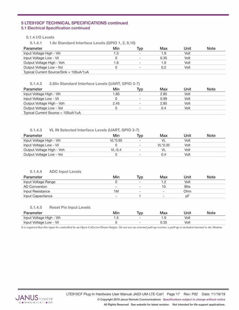
5 LTE910CF TECHNICAL SPECIFICATIONS continued5.1 Electrical Specification continued
5.1.4 I/O Levels 5.1.4.1 1.8v Standard Interface Levels (GPIO 1, 2, 9,10)
Parameter Min Typ Max Unit NoteInput Voltage High - Vih 1.5 - 1.9 Volt Input Voltage Low - Vil 0 - 0.35 Volt Output Voltage High - Voh 1.6 - 1.9 Volt Output Voltage Low - Vol 0 - 0.2 Volt Typical Current Source/Sink = 100uA/1uA
5.1.4.2 2.85v Standard Interface Levels (UART, GPIO 3-7)Parameter Min Typ Max Unit NoteInput Voltage High - Vih 1.85 - 2.85 Volt Input Voltage Low - Vil 0 - 0.99 Volt Output Voltage High - Voh 2.45 - 2.85 Volt Output Voltage Low - Vol 0 - 0.4 Volt Typical Current Source = 100uA/1uA
5.1.4.3 VL IN Selected Interface Levels (UART, GPIO 3-7)Parameter Min Typ Max Unit NoteInput Voltage High - Vih VL*0.65 - VL VoltInput Voltage Low - Vil 0 - VL*0.35 VoltOutput Voltage High - Voh VL-0.4 - VL VoltOutput Voltage Low - Vol 0 - 0.4 Volt
5.1.4.4 ADC Input LevelsParameter Min Typ Max Unit NoteInput Voltage Range 0 - 1.2 VoltAD Conversion - - 10 BitsInput Resistance 1M - - OhmInput Capacitance - 1 - pF
5.1.4.5 Reset Pin Input Levels Parameter Min Typ Max Unit NoteInput Voltage High - Vih 1.5 - 1.9 Volt Input Voltage Low - Vil 0 - 0.35 Volt
It is required that this input be controlled by an Open Collector/Drain Output. Do not use an external pull-up resistor, a pull-up is included internal to the Modem.
LTE910CF Plug-In Hardware User Manual JA03-UM-LTE-Cat1 Page 18 Rev: P02 Date: 11/19/19© Copyright 2019 Janus Remote Communications Specifications subject to change without notice
All Rights Reserved See website for latest revision. Not intended for life support applications.
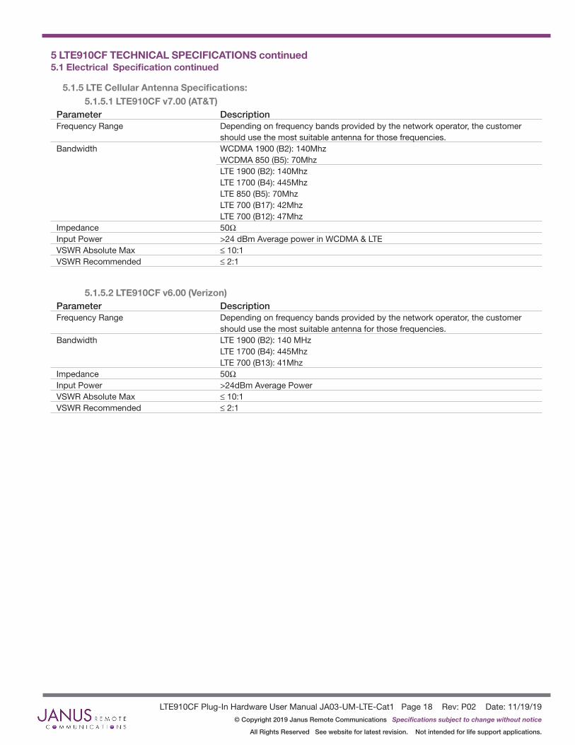
5.1.5 LTE Cellular Antenna Specifications: 5.1.5.1 LTE910CF v7.00 (AT&T)
Parameter DescriptionFrequency Range Depending on frequency bands provided by the network operator, the customer should use the most suitable antenna for those frequencies.Bandwidth WCDMA 1900 (B2): 140Mhz WCDMA 850 (B5): 70Mhz LTE 1900 (B2): 140Mhz LTE 1700 (B4): 445Mhz LTE 850 (B5): 70Mhz LTE 700 (B17): 42Mhz LTE 700 (B12): 47MhzImpedance 50ΩInput Power >24 dBm Average power in WCDMA & LTEVSWR Absolute Max ≤ 10:1VSWR Recommended ≤ 2:1
5.1.5.2 LTE910CF v6.00 (Verizon) Parameter DescriptionFrequency Range Depending on frequency bands provided by the network operator, the customer should use the most suitable antenna for those frequencies.Bandwidth LTE 1900 (B2): 140 MHz LTE 1700 (B4): 445Mhz LTE 700 (B13): 41MhzImpedance 50ΩInput Power >24dBm Average PowerVSWR Absolute Max ≤ 10:1VSWR Recommended ≤ 2:1
5 LTE910CF TECHNICAL SPECIFICATIONS continued5.1 Electrical Specification continued
LTE910CF Plug-In Hardware User Manual JA03-UM-LTE-Cat1 Page 19 Rev: P02 Date: 11/19/19© Copyright 2019 Janus Remote Communications Specifications subject to change without notice
All Rights Reserved See website for latest revision. Not intended for life support applications.
5 LTE910CF TECHNICAL SPECIFICATIONS continued5.1 Electrical Specification continued
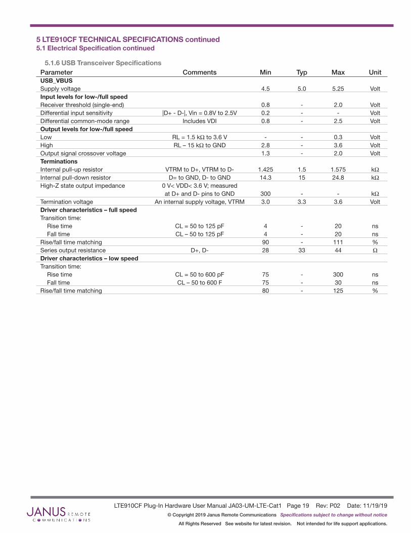
5.1.6 USB Transceiver SpecificationsParameter Comments Min Typ Max UnitUSB_VBUS Supply voltage 4.5 5.0 5.25 VoltInput levels for low-/full speed Receiver threshold (single-end) 0.8 - 2.0 VoltDifferential input sensitivity |D+ - D-|, Vin = 0.8V to 2.5V 0.2 - - VoltDifferential common-mode range Includes VDI 0.8 - 2.5 VoltOutput levels for low-/full speed Low RL = 1.5 kΩ to 3.6 V - - 0.3 VoltHigh RL – 15 kΩ to GND 2.8 - 3.6 VoltOutput signal crossover voltage 1.3 - 2.0 VoltTerminations Internal pull-up resistor VTRM to D+, VTRM to D- 1.425 1.5 1.575 kΩInternal pull-down resistor D= to GND, D- to GND 14.3 15 24.8 kΩHigh-Z state output impedance 0 V< VDD< 3.6 V; measured at D+ and D- pins to GND 300 - - kΩTermination voltage An internal supply voltage, VTRM 3.0 3.3 3.6 VoltDriver characteristics – full speed Transition time: Rise time CL = 50 to 125 pF 4 - 20 ns Fall time CL – 50 to 125 pF 4 - 20 nsRise/fall time matching 90 - 111 %Series output resistance D+, D- 28 33 44 ΩDriver characteristics – low speed Transition time: Rise time CL = 50 to 600 pF 75 - 300 ns Fall time CL – 50 to 600 F 75 - 30 nsRise/fall time matching 80 - 125 %
LTE910CF Plug-In Hardware User Manual JA03-UM-LTE-Cat1 Page 20 Rev: P02 Date: 11/19/19© Copyright 2019 Janus Remote Communications Specifications subject to change without notice
All Rights Reserved See website for latest revision. Not intended for life support applications.
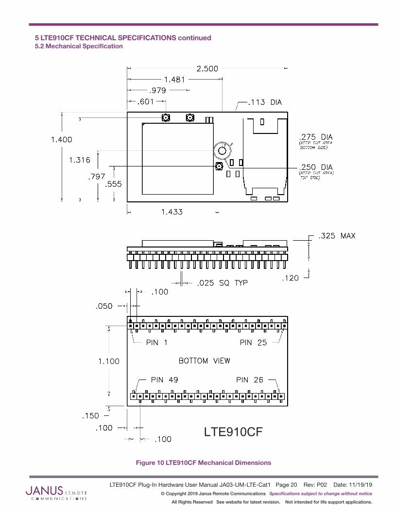
5 LTE910CF TECHNICAL SPECIFICATIONS continued5.2 Mechanical Specification
Figure 10 LTE910CF Mechanical Dimensions
LTE910CF
LTE910CF Plug-In Hardware User Manual JA03-UM-LTE-Cat1 Page 21 Rev: P02 Date: 11/19/19© Copyright 2019 Janus Remote Communications Specifications subject to change without notice
All Rights Reserved See website for latest revision. Not intended for life support applications.
6 Operation6.1 Powering ON/OFF
6.1.1 Powering ONPower the Modem ON by pulling the ON_OFF signal (Pin 19) to ground for at least five (5) seconds, then release.
6.1.2 Powering OFFThere are two methods to to turn OFF the Modem under normal circumstances:• Use the AT shutdown command (AT#SHDN)• Pull ON_OFF signal (Pin 19) to ground for at least three (3) seconds, then release.
In both instances, power can be removed from the modem once the PWRMON signal goes low.Under abnormal circumstances, the modem can be shut down using the RESET input (pin 20).
6.2. Communicating with the Modem
The default configuration of the modem has AT command ports available on the UART interface and the USBinterface.
6.2.1 UART InterfaceThe UART port operates at a the following default parameters:• Baud Rate: 115.2 kbps• Bits: 8• Stop Bits: 1• Parity: None• Hardware Handshaking
6.2.2 USB InterfaceThe USB port instantiates two serial modem connections as AT command ports by default. USB drivers areavailable from Telit or Janus.
6.3 Testing Communications• The cellular module should always respond to the attention command with ‘OK’. Send:
AT<cr>1
Note 1. “<cr>” designates a carriage return character.
The module will response with ‘OK’.
• Verify the module model. Send:
AT+CGMM<cr>
The response should be the Telit module model number.
• Verify the firmware version. Send:
AT+CGMR<cr>
The response will be the Telit module’s current firmware.
LTE910CF Plug-In Hardware User Manual JA03-UM-LTE-Cat1 Page 22 Rev: P02 Date: 11/19/19© Copyright 2019 Janus Remote Communications Specifications subject to change without notice
All Rights Reserved See website for latest revision. Not intended for life support applications.
6 Operation Continued
6.4 Cellular Network Communications
6.4.1 SIM CardAll LTE modems require a SIM card. The LTE910CF v6.00 and v7.00 use a 2FF ‘micro’ size SIM card.
6.4.2 Data Contexts - setting the APN6.4.2.1 Checking the Data Contexts
Data connections require that the carrier’s Access Point Name (APN) be properly set in the data contexts using the AT+CGDCONT command. In LTE modules, some contexts may be assigned for the carrier’s use.
The data contexts can be checked by entering the following command:
AT+CGDCONT?<cr>
The module will respond with the current data contex settings.NOTE: A SIM card must be present to read the data contexts.The default settings for the LTE Cat.M1 modems are as follows:
LTE910CF v7.00:
+CGDCONT: 1,”IPV4V6”,””,””,0,0
Context ID 1 is for the user’s data connection. It must be set to an appropriate APN.
LTE910CF v6.00:
+CGDCONT: 1,”IPV4V6”,”vzwims”,””,0,0
+CGDCONT: 2,”IPV4V6”,”vzwadmin”,””,0,0
+CGDCONT: 3,”IPV4V6”,”vzwinternet”,””,0,0
+CGDCONT: 4,”IPV4V6”,”vzwapp”,””,0,0
+CGDCONT: 5,”IPV4V6”,”vzw800”,””,0,0
+CGDCONT: 6,”IPV4V6”,”vzwclass6”,””,0,0
Context ID 3 is for the user’s data connection; it is set to the default APN for Verizon.
6.4.2.2 Setting the Data ContextsMake sure you are using an acceptable APN or the device will not register on the network. For example, a general APN for AT&T is “nxtgenphone”.
To set a data context with this APN, enter the following:
AT+CGDCONT=1,”IPV4V6”,”nxtgenphone”<cr>
and wait for the “OK” response.NOTE: Carrier services such as a staic IP address or VPN may require a specialized APN.
LTE910CF Plug-In Hardware User Manual JA03-UM-LTE-Cat1 Page 23 Rev: P02 Date: 11/19/19© Copyright 2019 Janus Remote Communications Specifications subject to change without notice
All Rights Reserved See website for latest revision. Not intended for life support applications.
6 Operation Continued
6.4 Cellular Network Communications continued
6.4.3 Signal StrengthSignal strength can be checked as follows. Enter:
AT+CSQ<cr>
The default response format will contain two numbers:
+CSQ: 17,0
The first number is the rssi (received signal strength indication) and the second is ber (bit error rate).
The rssi can be interpreted as follows:
10-14 Okay
15-20 Good
20+ Excellent.
Anyting below 10 would be considered marginal.
A response of 99 indicates no signal.
6.4.4 RegistrationNetwork registration can be checked as follows. Enter:
AT+CEREG?<cr>
A response of +CEREG:0,1 or +CEREG: 0,5 indicates the device is registered to the home network or roaming, respectively.
If response is different than this, please refer to the Telit AT command reference document for more information
6.5 Data Communications
The modem incorporates a TCP/IP stack that can be used to directly send data using AT commands. Alternativly, an external host can be used to make a PPP connection.
6.5.1 Data Communications - Using the Internal StackTo send data using the internal stack, a data context must be activated.
Activate the context as follows:
LTE910CF v7.00:
Enter:
AT#SGACT=1,1<cr>
LTE910CF v6.00:
Enter:
AT#SGACT=3,1<cr>
If successful, the modem will respond with an IP address assigned by the carrier. Data can be sent to a host with a socket dial command. Enter:
AT#SD=<connid>,0,80,<IPaddr>
where <connid> is the user data context (1 for LTE910 v7.00, 3 for LTE910 v6.00) and <IPaddr> is a text string (in quotes) containing a dotted IP address or a DNS resovable host name.
The modem will respond with CONNECT and any data entererd thereafter will be sent to the connected host. Enter the escape sequence:
+++
to suspend the connection.
See the Telit IP Easy User Guide and the Telit AT Commands Guide for more information.
LTE910CF Plug-In Hardware User Manual JA03-UM-LTE-Cat1 Page 24 Rev: P02 Date: 11/19/19© Copyright 2019 Janus Remote Communications Specifications subject to change without notice
All Rights Reserved See website for latest revision. Not intended for life support applications.
6 Operation continued6.5 Data Communications cintinued
6.5.2 PPP DialingIn a hosted system (e.g. Linux) the host TCP/IP stack can be used. A PPP connection is initiated using the ATD dialing command. Depending on the script or application performing the PPP connection, you may have to change the numeric digit in the PPP AT dialing command that designates the context to use.
The dialing string for the LTE910CF v7.00 would be:
ATD*99***1#<cr>
Where the ‘1’ digit selects the #1 data context set with the +CDGCONT command.
Simillarly the dialing string for the LTE910CF v6.00 would be:
ATD*99***3#<cr>
Where the ‘3’ digit selects the #3 data context set with the +CDGCONT command.
6.6 SMS
SMS allows you to send a text message (max 160 characters) to a SMS capable unit. • Set the SMS mode to text. This setting is not persistant; it must be entered every power cycle.
AT+CMGF=1<cr>
• To enter the receiving subscriber unit phone number and message enter:
AT+CMGS=”8885551234”<cr>
Wait for response ”>” then enter message text .
Enter
<ctrl-z>
to end the message text and send it.
LTE910CF Plug-In Hardware User Manual JA03-UM-LTE-Cat1 Page 25 Rev: P02 Date: 11/19/19© Copyright 2019 Janus Remote Communications Specifications subject to change without notice
All Rights Reserved See website for latest revision. Not intended for life support applications.
7 Design Considerations7.1 Minimum Required Module Pin Connects
Pin Signal Function Note 1 VBATT Main power supply 2 VBATT Main power supply 12 GND Ground 25 GND Ground 26 GND Ground 39 GND Ground 49 GND Ground 9 TXD Serial data input (TXD) from DTE 4 RXD Serial data output to DTE 11 RTS Input for request to send signal (RTS) from DTE 2 19 ON/OFF Input command for switching power ON or OFF(toggle command) 20 RESET Reset input
Note: 1. If the application uses USB as the main interface to the Modem, this is sufficient to capture any debug or trace data, provided the application can export the diagnostic port externally. 2. RTS must be connected to ground if flow control is not used.
7.2 Debug:
Debug of the Modems in production
To test and debug the mounting of the Modem, we strongly recommend test pads on the host PCB. This will allow verification of the connection between the module itself and the application and to test the performance of the module connecting it with an external computer.
Depending on the customer application, these pads include, but are not limited to the following signals:
• TXD
• RXD
• ON/OFF
• RESET
• GND
• VBATT
• TX_TRACE
• RX_TRACE
• PWRMON
• USB D+
• USB D-
• USB V_BUS
LTE910CF Plug-In Hardware User Manual JA03-UM-LTE-Cat1 Page 26 Rev: P02 Date: 11/19/19© Copyright 2019 Janus Remote Communications Specifications subject to change without notice
All Rights Reserved See website for latest revision. Not intended for life support applications.
APPENDICESApprovals
LTE910CF v7.00 FCC: RI7LE910NAV2
IC: 5131A-LE910NAV2
PTCRB, AT&T, Rogers (Canada)
LTE910CF v6.00 FCC: RI7LE910SVV2
Verizon
Antenna Care and Replacement
Do not use the Modem with a damaged antenna.
Buy the antenna from an approved suppliers list. Using unauthorized antennas, modifications, or attachments could damage the Modem and may violate local RF emission regulations or invalidate type approval.
Abbreviations3GPP 3rd Generation Partnership ProjectAC Alternating CurrentADC Analog To Digital Converter
APN Access Point NameBER Bit Error RateCD Carrier DetectCDMA Code Division Multiple AccessCTS Clear To SendDB DecibelDC Direct CurrentDCE Data Communications EquipmentDSR Data Set ReadyDTMF Dual-tone multi-frequencyDTR DTE Ready
GNSS Global Navigation Satellite SystemGPIO General Purpose Input Output
HSPA High Speed Packet AccessGPRS General Packet Radio Service
GSM Global System Mobile
IoT Internet of ThingsLED Light Emitting Diode
LTE Long Term EvolutionM2M Machine To MachineRF Radio FrequencyRI Ring IndicatorRSSI Received Signal Strength IndicationRTS Request To SendRxD Received DataSMS Short Message ServiceTTFF Time To First FixTxD Transmitted DataUICC Universal Integrated Circuit CardUMTS Universal Mobile Telecommunications SystemUSIM Universal Subscriber Identity ModuleVSWR Voltage Standing Wave Ratio
WCDMA Wideband Code Division Multiplexing Access
LTE910CF CAT1 Embedded Cellular Modem User Manual
Revision History Revision Revision Date NoteP00 06/21/17 Preliminary LTE910CF CAT1 Individual Plug-In User ManualP01 04/04/18 Addition of documentation and block diagram edit
Ordering Information
Ordering Information DescriptionLTE910CF v6.00 LTE Cat.1 Plug-In Modem - VerizonLTE910CF v7.00 LTE Cat.1 Plug-In Modem - AT&T
Division of The Connor-Winfield Corporation2359 Diehl Road • Aurora, IL 60502
Phone: 630.499.2121 • [email protected]
www.janus-rc.com