Embed Size (px)
Citation preview

LTM8042/LTM8042-1
180421fb
For more information www.linear.com/LTM8042
TYPICAL APPLICATION
FEATURES DESCRIPTION
µModule Boost LED Driver and Current Source
The LTM®8042 is a complete µModule® Boost LED Driver specifically designed to drive LEDs up to 1A, while the LTM8042-1 drives up to 350mA. It combines a boost power topology with a unique current loop to operate as a constant-current source. The PWM input provides as much as 3000:1 LED dimming, while 10:1 analog dimming can be accomplished by a single resistor or analog voltage applied to the CTL pin. As with any boost topology, the LTM8042/LTM8042-1 has an uninterrupted current path between its input and output and is thus intolerant to a short-circuit or overload from the output to ground.
# WHITE LEDS LED CURRENT 12VIN 24VIN
6 1A LTM8042
7 350mA LTM8042-1
8 1A LTM8042
9 350mA LTM8042-1
The LTM8042/LTM8042-1 is packaged in a thermally enhanced, compact overmolded land grid array (LGA) package. The LTM8042/LTM8042-1 is Pb-free and a RoHS compliant.
µModule Boost LED Driver, Driving 8 White LEDs at 1A
APPLICATIONS
n True Color PWM™ with 3000:1 Dimming Ration Operates in Boost, Buck Mode or Buck-Boost Moden Wide Input Voltage Range: Operation from 3V to 30V Transient Protection to 40Vn Gate Driver for Optional PWM Dimming with
P-channel MOSFETn Adjustable Frequency: 250kHz to 2MHzn Constant-Current and Constant-Voltage Regulationn Low Shutdown Current: <1μA n RoHS Compliant Package with Gold Pad Finishn Tiny, Low Profile (9mm × 15mm × 2.82mm)
Surface Mount LGA Package
n Display Backlightingn Automotive and Avionic Lightingn Illuminationn Scanners
Efficiency vs VIN
L, LT, LTC, LTM, Linear Technology, the Linear logo and µModule are registered trademarks and True Color PWM is a trademark of Linear Technology Corporation. All other trademarks are the property of their respective owners.
VIN (V)16
87
EFFI
CIEN
CY (%
)
1918
97
80421 TA01b
17 20 232221 2524 26
91
90
93
89
88
95
92
94
96
80421 TA01a
LTM8042
RT GND CTL
VCC
RUN
BSTIN/BKLED–
PWM
SYNC
TGEN
SS
VIN16V TO 26V
LED+
TG
BSTOUT/BKIN
4.7µF
33.2kfSW = 550kHz
4.7µF
1A
UP TO 26.8V
LTM8042/LTM8042-1
280421fb
For more information www.linear.com/LTM8042
PART NUMBER PAD OR BALL FINISH
PART MARKING*
PACKAGE TYPE MSL RATINGTEMPERATURE RANGE (Note 4)DEVICE FINISH CODE
LTM8042EV#PBF Au (RoHS) LTM8042V e4 LGA 3 –40°C to 125°C
LTM8042IV#PBF Au (RoHS) LTM8042V e4 LGA 3 –40°C to 125°C
LTM8042EV-1#PBF Au (RoHS) LTM8042V-1 e4 LGA 3 –40°C to 125°C
LTM8042IV-1#PBF Au (RoHS) LTM8042V-1 e4 LGA 3 –40°C to 125°C
Consult Marketing for parts specified with wider operating temperature ranges. *Device temperature grade is indicated by a label on the shipping container. Pad or ball finish code is per IPC/JEDEC J-STD-609.• Terminal Finish Part Marking:
www.linear.com/leadfree
• Recommended LGA and BGA PCB Assembly and Manufacturing Procedures: www.linear.com/umodule/pcbassembly
• LGA and BGA Package and Tray Drawings: www.linear.com/packaging
PIN CONFIGURATIONABSOLUTE MAXIMUM RATINGS
VCC, RUN, PWM, TGEN, BSTIN/BKLED– ...................40VBSTOUT/BKIN, LED+ ................................................43VCTL, SYNC ..................................................................6VInternal Operating Temperature(Notes 3, 4) ........................................... –40°C to 125°CMaximum Reflow Body Temperature .................. 245°CStorage Temperature ............................. –55°C to 125°C
(Note 1)
A B C D E F
BANK 1
BANK 3 BANK 4
TG
BANK 5
BSTOUT/BKIN LED+
BANK 2
GND
G
RUN SYNC RT SS PWM
H J K L
7
6
5
4
3
2
1
TGEN
CTL
VCC
LGA PACKAGE77-LEAD (15mm × 9mm × 2.82mm)
BSTIN/BKLED–
TJMAX = 125°C, θJA = 15.7°C/W, θJCtop = 13.6°C/W,
θJCbottom = 4.5°C/W, θJB = 9.4°C/W θ VALUES DETERMINED PER JESD 51-12
WEIGHT = 1.1g
ORDER INFORMATION

LTM8042/LTM8042-1
380421fb
For more information www.linear.com/LTM8042
ELECTRICAL CHARACTERISTICS
Note 1: Stresses beyond those listed under Absolute Maximum Ratings may cause permanent damage to the device. Exposure to any Absolute Maximum Rating condition for extended periods may affect device reliability and lifetime.Note 2: Absolute maximum voltage at VCC, RUN, PWM, TGEN, BSTIN/BKLED– pins is 40V for non-repetitive one second transients and 30V for continuous operation.Note 3: The LTM8042E/LTM8042E-1 are guaranteed to meet performance specifications from 0°C to 125°C ambient. Specifications over the full –40°C to 125°C internal operating temperature range are assured by design, characterization and correlation with statistical process controls.
The l denotes the specifications which apply over the full internal operating temperature range, otherwise specifications are at TA = 25°C. VCC = 5V, buck mode with 4Ω load.
SYMBOL PARAMETER CONDITIONS MIN TYP MAX UNITS
VCC(MIN) Minimum Input DC Voltage l 3 V
ILED LTM8042 LED Current LTM8042-1 LED Current
CTL Open RCTL = 6.81k CTL Open RCTL = 6.81k
0.9 0.45 0.34 0.17
0.5
1.05 0.55 0.39 0.20
A A A A
VCLAMP Open LED Clamp Voltage Boost Mode, LED+ Open 36 V
∆IOUT/IOUT Output Current Line Regulation LTM8042, 6V < BSTOUT/BKIN < 30V LTM8042-1, 6V < BSTOUT/BKIN < 30V
0.5 0.5
% %
IQVCC VCC Supply Current PWM = 0V RUN = 0V
4.2 0.1
1
mA µA
fSW Switching Frequency RT = 90.9k RT = 22.1k RT = 6.04k
0.22 0.68 1.7
0.25 0.8 2
0.27 0.92 2.3
MHz MHz MHz
ISS Soft-Start Pin Current SS = 0.5V, Out of Pin 6 9 12 µA
fSYNC Synchronization Frequency Range 0.3 2.5 MHz
ISYNC SYNC Pull-Down Current (Into the Pin) VSYNC = 2V 60 µA
VSYNC(IL) SYNC Input Low 0.4 V
VSYNC(IH) SYNC Input High 1.5 V
ICTL CTL Input Bias Current CTL = 0V, Flows Out of Pin 100 µA
VRUN(IH) RUN Input Voltage High 1.5 V
VRUN(IL) RUN Input Voltage Low 0.4 V
IRUN RUN Pin Bias Current 60 100 µA
VPWM(IH) PWM Input Voltage High 1.5 V
VPWM(IL) PWM Input Voltage Low 0.4 V
IPWM PWM Pin Bias Current 60 120 µA
VTG(OH) TG Output High Voltage Relative to LED+, 100k from LED+ to TG 0 V
VTG(OL) TG Output Low Voltage Relative to LED+, 100k from LED+ to TG –7 V
VTGEN(IH) TGEN Input Voltage High PWM = 0V 1.5 V
VTGEN(IL) TGEN Input Voltage Low 0.4 V
ITGEN TGEN Pin Bias Current 100 200 µA
The LTM8042I/LTM8042I-1 are guaranteed to meet specifications over the full –40°C to 125°C internal operating temperature range. Note that the maximum internal temperature is determined by specific operating conditions in conjunction with board layout, the rated package thermal resistance and other environmental factors.Note 4: This device includes overtemperature protection that is intended to protect the device during momentary overload conditions. Junction temperature will exceed the maximum internal operating temperature when overtemperature protection is active. Continuous operation above the specified maximum operating junction temperature may impair device reliability.
LTM8042/LTM8042-1
480421fb
For more information www.linear.com/LTM8042
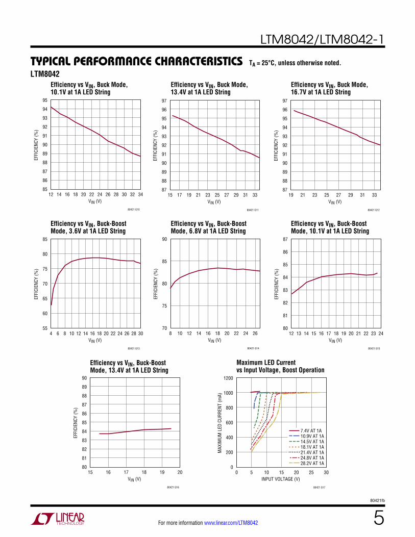
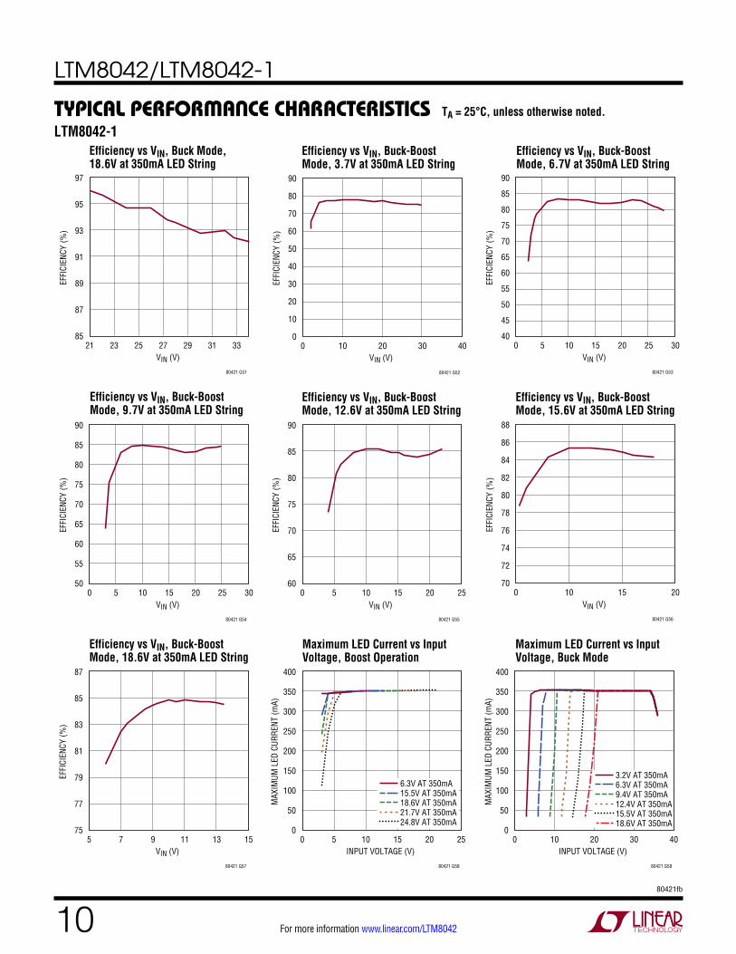
TYPICAL PERFORMANCE CHARACTERISTICS
Efficiency vs VIN, Boost Operation, 16.7V at 1A LED String
Efficiency vs VIN, Boost Operation, 20.1V at 1A LED String
Efficiency vs VIN, Boost Operation, 23.4V at 1A LED String
Efficiency vs VIN, Boost Operation, 26.8V at 1A LED String
Efficiency vs VIN, Buck Mode, 3.5V at 1A LED String
Efficiency vs VIN, Buck Mode, 6.8V at 1A LED String
Efficiency vs VIN, Boost Operation, 6.8V at 1A LED String
Efficiency vs VIN, Boost Operation, 10.1V at 1A LED String
Efficiency vs VIN, Boost Operation, 13.4V at 1A LED String
TA = 25°C, unless otherwise noted.
LTM8042
VIN (V)4
80
EFFI
CIEN
CY (%
)
81
82
83
84
85
86
5
90
80421 G01
6
87
88
89
VIN (V)5
80
EFFI
CIEN
CY (%
)
82
84
87
94
80421 G02
6 9 10
86
88
90
92
VIN (V)7
85
EFFI
CIEN
CY (%
)
87
86
88
109
95
80421 G03
8 1211 13
89
90
92
91
93
94
VIN (V)8
80
EFFI
CIEN
CY (%
)
1413
94
90
92
80421 G04
1211109 15 16
84
82
86
88
VIN (V)11
83
EFFI
CIEN
CY (%
)
85
1713
97
80421 G05
12 14 1615 18 19
87
91
89
93
95
VIN (V)12
83
EFFI
CIEN
CY (%
)
1514
97
80421 G06
13 16 191817 2120 22
91
89
93
87
85
95
VIN (V)16
87
EFFI
CIEN
CY (%
)
1918
97
80421 G07
17 20 232221 2524 26
91
90
93
89
88
95
92
94
96
VIN (V)4
75
EFFI
CIEN
CY (%
)
1816
89
80421 G08
14 201086 12 262422 30 3228 34
77
81
85
79
83
87
VIN (V)8
80
EFFI
CIEN
CY (%
)
1816
94
80421 G09
14 2010 12 262422 30 3228 34
82
86
90
84
88
92
LTM8042/LTM8042-1
580421fb
For more information www.linear.com/LTM8042
TYPICAL PERFORMANCE CHARACTERISTICS
Efficiency vs VIN, Buck-Boost Mode, 3.6V at 1A LED String
Efficiency vs VIN, Buck-Boost Mode, 6.8V at 1A LED String
Efficiency vs VIN, Buck-Boost Mode, 10.1V at 1A LED String
Efficiency vs VIN, Buck Mode, 10.1V at 1A LED String
Efficiency vs VIN, Buck Mode, 13.4V at 1A LED String
Efficiency vs VIN, Buck Mode, 16.7V at 1A LED String
TA = 25°C, unless otherwise noted.
Maximum LED Current vs Input Voltage, Boost Operation
LTM8042
Efficiency vs VIN, Buck-Boost Mode, 13.4V at 1A LED String
VIN (V)12
85
EFFI
CIEN
CY (%
)
1816
93
95
94
80421 G10
14 20 262422 30 3228 34
86
88
90
87
89
92
91
VIN (V)15
87
EFFI
CIEN
CY (%
)
19
95
97
96
80421 G11
17 21 272523 3129 33
88
90
92
89
91
94
93
VIN (V)19
87
EFFI
CIEN
CY (%
)
95
97
96
80421 G12
21 272523 3129 33
88
90
92
89
91
94
93
VIN (V)4
55
EFFI
CIEN
CY (%
)
2624
85
80421 G13
20 22 28 301086 12 14 16 18
75
70
80
60
65
VIN (V)8
70
EFFI
CIEN
CY (%
)
262422
90
80421 G14
2010 12 14 16 18
85
75
80
VIN (V)12
80
EFFI
CIEN
CY (%
)
242322
87
80421 G15
2013 14 15 16 17 18 2119
85
86
81
82
83
84
VIN (V)15
80
EFFI
CIEN
CY (%
)
20
90
80421 G16
16 17 18 19
85
86
81
82
83
84
88
89
87
INPUT VOLTAGE (V)0
0
MAX
IMUM
LED
CUR
RENT
(mA)
2015
1200
80421 G17
105 25 30
1000
200
800
400
600
7.4V AT 1A10.9V AT 1A14.5V AT 1A18.1V AT 1A21.4V AT 1A24.8V AT 1A28.2V AT 1A
LTM8042/LTM8042-1
680421fb
For more information www.linear.com/LTM8042
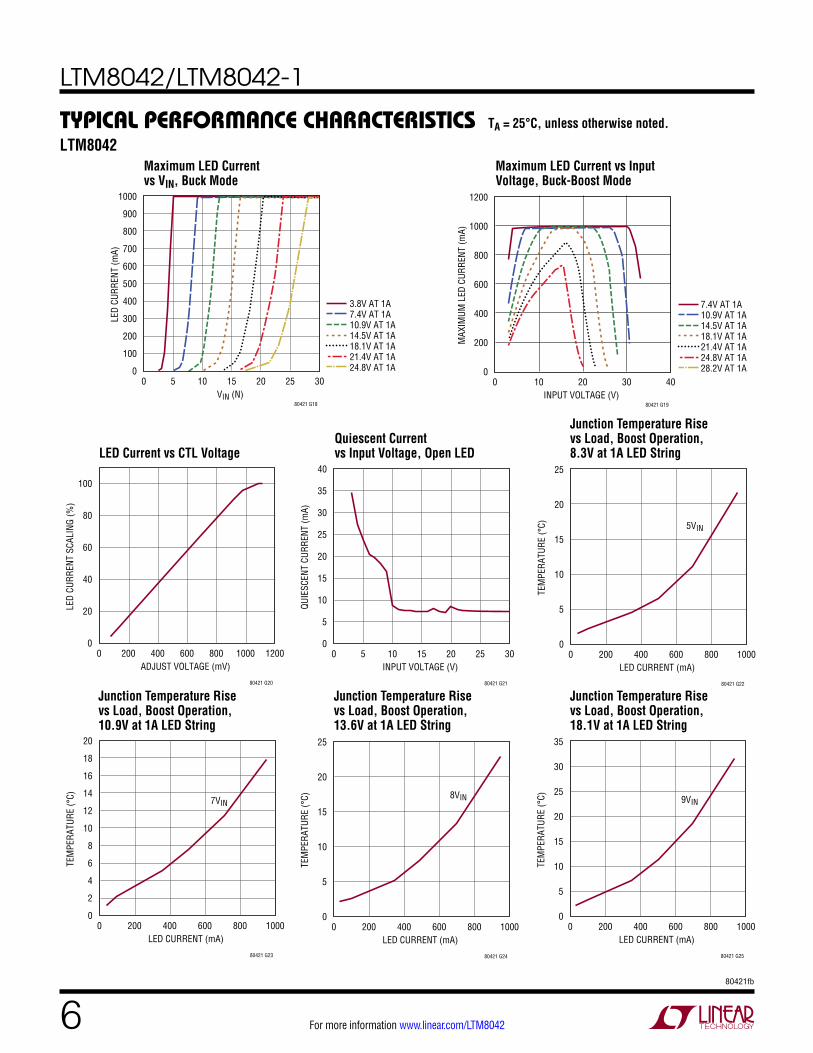
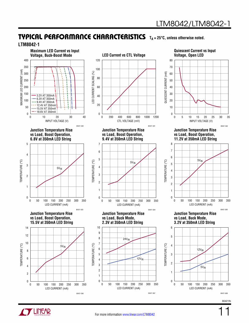
TYPICAL PERFORMANCE CHARACTERISTICS
LED Current vs CTL VoltageQuiescent Current vs Input Voltage, Open LED
Junction Temperature Rise vs Load, Boost Operation, 8.3V at 1A LED String
Maximum LED Current vs VIN, Buck Mode
Maximum LED Current vs Input Voltage, Buck-Boost Mode
Junction Temperature Rise vs Load, Boost Operation, 18.1V at 1A LED String
Junction Temperature Rise vs Load, Boost Operation, 13.6V at 1A LED String
Junction Temperature Rise vs Load, Boost Operation, 10.9V at 1A LED String
VIN (N)0
0
LED
CURR
ENT
(mA)
2015
1000
80421 G18
105 25 30
900
200
100
800
400
600
300
500
700
3.8V AT 1A7.4V AT 1A10.9V AT 1A14.5V AT 1A18.1V AT 1A21.4V AT 1A24.8V AT 1A
INPUT VOLTAGE (V)0
0
MAX
IMUM
LED
CUR
RENT
(mA)
20
1200
80421 G19
10 30 40
1000
200
800
400
600
7.4V AT 1A10.9V AT 1A14.5V AT 1A18.1V AT 1A21.4V AT 1A24.8V AT 1A28.2V AT 1A
ADJUST VOLTAGE (mV)0
0
LED
CURR
ENT
SCAL
ING
(%)
800600
100
80421 G20
400200 1000 1200
20
80
40
60
INPUT VOLTAGE (V)0
0
QUIE
SCEN
T CU
RREN
T (m
A)
2015
40
80421 G21
105 25 30
5
30
10
20
35
15
25
LED CURRENT (mA)0
0
TEM
PERA
TURE
(°C)
600400
25
80421 G22
200 800 1000
20
15
5
10
5VIN
LED CURRENT (mA)0
0
TEM
PERA
TURE
(°C)
600400
20
80421 G23
200 800 1000
14
12
18
16
8
6
4
2
10
7VIN
LED CURRENT (mA)0
0
TEM
PERA
TURE
(°C)
600400
25
80421 G24
200 800 1000
20
15
5
10
8VIN
LED CURRENT (mA)0
0
TEM
PERA
TURE
(°C)
600400
35
80421 G25
200 800 1000
20
15
30
25
5
10
9VIN
TA = 25°C, unless otherwise noted.
LTM8042
LTM8042/LTM8042-1
780421fb
For more information www.linear.com/LTM8042
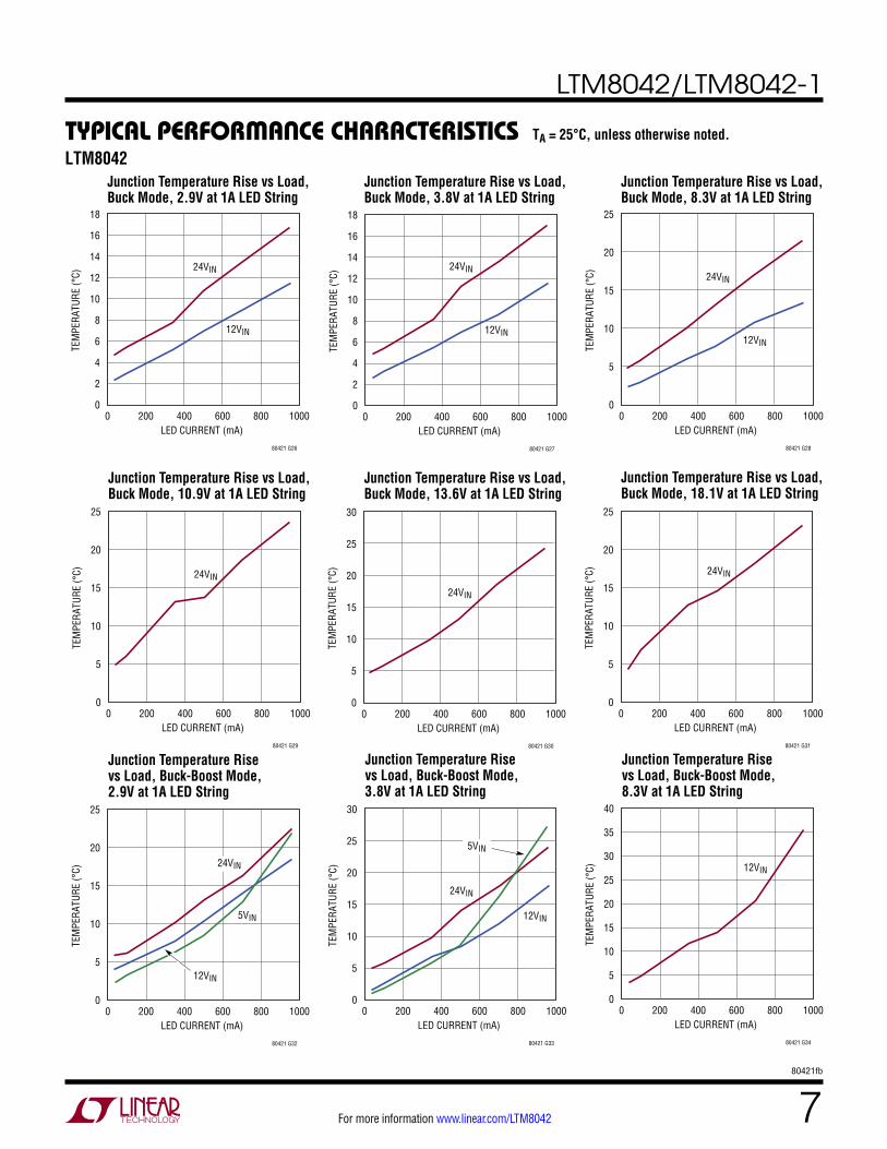
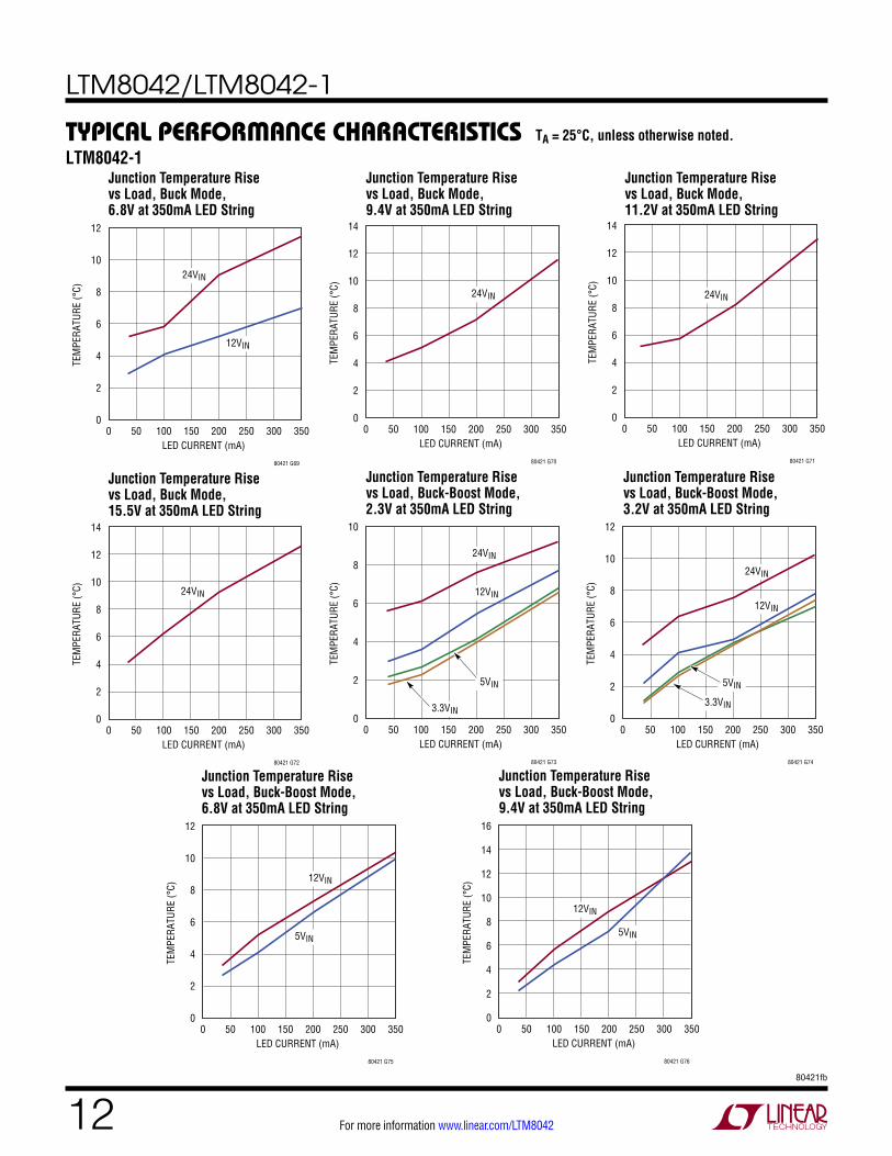
TYPICAL PERFORMANCE CHARACTERISTICS
Junction Temperature Rise vs Load, Buck Mode, 10.9V at 1A LED String
Junction Temperature Rise vs Load, Buck-Boost Mode, 3.8V at 1A LED String
Junction Temperature Rise vs Load, Buck-Boost Mode, 8.3V at 1A LED String
Junction Temperature Rise vs Load, Buck-Boost Mode, 2.9V at 1A LED String
Junction Temperature Rise vs Load, Buck Mode, 2.9V at 1A LED String
Junction Temperature Rise vs Load, Buck Mode, 3.8V at 1A LED String
Junction Temperature Rise vs Load, Buck Mode, 8.3V at 1A LED String
Junction Temperature Rise vs Load, Buck Mode, 13.6V at 1A LED String
Junction Temperature Rise vs Load, Buck Mode, 18.1V at 1A LED String
LED CURRENT (mA)0
0
TEM
PERA
TURE
(°C)
600400
18
80421 G26
200 800 1000
10
12
6
8
16
14
2
4
12VIN
24VIN
LED CURRENT (mA)0
0
TEM
PERA
TURE
(°C)
600400
18
80421 G27
200 800 1000
10
12
6
8
16
14
2
4
12VIN
24VIN
LED CURRENT (mA)0
0
TEM
PERA
TURE
(°C)
600400
25
80421 G28
200 800 1000
10
5
20
15
12VIN
24VIN
LED CURRENT (mA)0
0
TEM
PERA
TURE
(°C)
600400
25
80421 G29
200 800 1000
10
5
20
1524VIN
LED CURRENT (mA)0
0
TEM
PERA
TURE
(°C)
600400
30
25
80421 G30
200 800 1000
10
5
20
1524VIN
LED CURRENT (mA)0
0
TEM
PERA
TURE
(°C)
600400
25
80421 G31
200 800 1000
10
5
20
15
24VIN
LED CURRENT (mA)0
0
TEM
PERA
TURE
(°C)
600400
25
80421 G32
200 800 1000
10
5
20
15
12VIN
5VIN
24VIN
LED CURRENT (mA)0
0
TEM
PERA
TURE
(°C)
600400
30
25
80421 G33
200 800 1000
10
5
20
1512VIN
24VIN
5VIN
LED CURRENT (mA)0
0
TEM
PERA
TURE
(°C)
600400
40
25
80421 G34
200 800 1000
10
5
20
35
30
15
12VIN
TA = 25°C, unless otherwise noted.
LTM8042

LTM8042/LTM8042-1
880421fb
For more information www.linear.com/LTM8042
TYPICAL PERFORMANCE CHARACTERISTICS
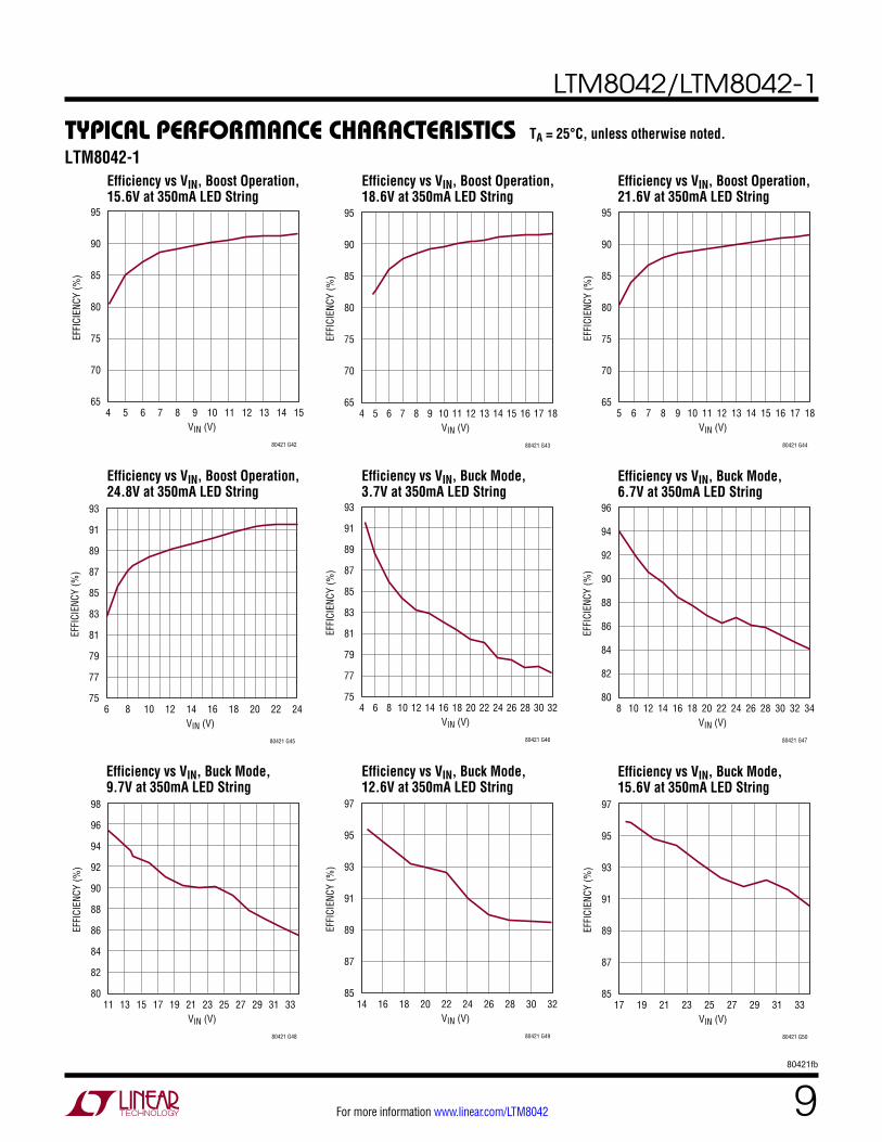
RUN Pin Current vs Voltage
Efficiency vs VIN, Boost Operation, 6.7V at 350mA LED String
Junction Temperature Rise vs Load, Buck-Boost Mode, 10.9V at 1A LED String
Junction Temperature Rise vs Load, Buck-Boost Mode, 13.6V at 1A LED String
Junction Temperature Rise vs Load, Buck-Boost Mode, 15.5V at 350mA LED String
LTM8042-1
LED CURRENT (mA)0
0
TEM
PERA
TURE
(°C)
600400
50
25
80421 G35
200 800 1000
10
5
20
35
30
45
40
15
12VIN
LED CURRENT (mA)0
0
TEM
PERA
TURE
(°C)
600400
60
80421 G36
200 800 1000
10
20
30
50
4016VIN12VIN
LED CURRENT (mA)0
0
TEM
PERA
TURE
(°C)
200100 250150
25
80421 G37
50 300 350
5
10
20
15
12VIN
RUN VOLTAGE (V)0
0
RUN
CURR
ENT
(µA)
2010
160
80421 G38
30 40
20
60
40
80
140
120
100
LTM8042/LTM8042-1
TA = 25°C, unless otherwise noted.
LTM8042
Efficiency vs VIN, Boost Operation, 9.7V at 350mA LED String
Efficiency vs VIN, Boost Operation, 12.6V at 350mA LED String
VIN (V)2
65
EFFI
CIEN
CY (%
)
3 4
95
80421 G39
5 6
70
80
75
85
90
VIN (V)2.5
65
EFFI
CIEN
CY (%
)
4.5
95
80421 G40
6.5 8.5
70
80
75
85
90
VIN (V)3
65
EFFI
CIEN
CY (%
)
5 7
95
80421 G41
9 11
70
80
75
85
90
LTM8042/LTM8042-1
980421fb
For more information www.linear.com/LTM8042
TYPICAL PERFORMANCE CHARACTERISTICS
Efficiency vs VIN, Buck Mode, 6.7V at 350mA LED String
Efficiency vs VIN, Buck Mode, 9.7V at 350mA LED String
Efficiency vs VIN, Buck Mode, 12.6V at 350mA LED String
Efficiency vs VIN, Buck Mode, 3.7V at 350mA LED String
Efficiency vs VIN, Buck Mode, 15.6V at 350mA LED String
TA = 25°C, unless otherwise noted.
LTM8042-1Efficiency vs VIN, Boost Operation, 15.6V at 350mA LED String
Efficiency vs VIN, Boost Operation, 18.6V at 350mA LED String
Efficiency vs VIN, Boost Operation, 21.6V at 350mA LED String
Efficiency vs VIN, Boost Operation, 24.8V at 350mA LED String
VIN (V)4
65
EFFI
CIEN
CY (%
)
1265 137 8 109 11
95
80421 G42
14 15
70
80
90
75
85
VIN (V)4
65
EFFI
CIEN
CY (%
)
1265 137 8 109 11
95
80421 G43
14 15 16 17 18
70
80
90
75
85
VIN (V)5
65
EFFI
CIEN
CY (%
)
126 137 8 109 11
95
80421 G44
14 15 16 17 18
70
80
90
75
85
VIN (V)6
75
EFFI
CIEN
CY (%
)
128 10
93
91
80421 G45
14 16 18 20 22 24
77
81
89
79
85
83
87
VIN (V)4
75
EFFI
CIEN
CY (%
)
128
93
91
80421 G46
16 20 24 286 1410 18 22 26 30 32
77
81
89
79
85
83
87
VIN (V)8
80
EFFI
CIEN
CY (%
)
12
96
94
80421 G47
16 20 24 281410 18 22 26 30 32 34
84
92
82
88
86
90
VIN (V)11
80
EFFI
CIEN
CY (%
)
15
98
96
94
80421 G48
19 21 25 291713 23 27 31 33
84
92
82
88
86
90
VIN (V)14
85
EFFI
CIEN
CY (%
)
97
80421 G49
18 20 24 2816 22 26 30 32
89
87
93
91
95
VIN (V)17
85
EFFI
CIEN
CY (%
)
97
80421 G50
21 23 2719 25 29 31 33
89
87
93
91
95
LTM8042/LTM8042-1
1080421fb
For more information www.linear.com/LTM8042
TYPICAL PERFORMANCE CHARACTERISTICS
Maximum LED Current vs Input Voltage, Boost Operation
Maximum LED Current vs Input Voltage, Buck Mode
Efficiency vs VIN, Buck-Boost Mode, 6.7V at 350mA LED String
Efficiency vs VIN, Buck-Boost Mode, 9.7V at 350mA LED String
Efficiency vs VIN, Buck-Boost Mode, 12.6V at 350mA LED String
INPUT VOLTAGE (V)0
0
MAX
IMUM
LED
CUR
RENT
(mA)
2015
400
80421 G58
105 25
300
350
200
50
250
100
1506.3V AT 350mA15.5V AT 350mA18.6V AT 350mA21.7V AT 350mA24.8V AT 350mA
INPUT VOLTAGE (V)0
0
MAX
IMUM
LED
CUR
RENT
(mA)
20
400
80421 G59
10 30 40
350
50
300
100
200
150
250
3.2V AT 350mA6.3V AT 350mA9.4V AT 350mA12.4V AT 350mA15.5V AT 350mA18.6V AT 350mA
Efficiency vs VIN, Buck-Boost Mode, 3.7V at 350mA LED String
TA = 25°C, unless otherwise noted.
LTM8042-1Efficiency vs VIN, Buck Mode, 18.6V at 350mA LED String
Efficiency vs VIN, Buck-Boost Mode, 15.6V at 350mA LED String
Efficiency vs VIN, Buck-Boost Mode, 18.6V at 350mA LED String
VIN (V)21
85
EFFI
CIEN
CY (%
)
97
80421 G51
23 2725 29 31 33
89
87
93
91
95
VIN (V)0
0
EFFI
CIEN
CY (%
)
90
80421 G52
10 20 30 40
40
20
70
60
30
10
50
80
VIN (V)0
40
EFFI
CIEN
CY (%
)
90
80421 G53
10 205 15 25 30
60
50
75
85
70
55
45
65
80
VIN (V)0
50
EFFI
CIEN
CY (%
)
90
80421 G54
10 205 15 25 30
60
75
85
70
55
65
80
VIN (V)0
60
EFFI
CIEN
CY (%
)
90
80421 G55
10 205 15 25
75
85
70
65
80
VIN (V)0
70
EFFI
CIEN
CY (%
)
88
80421 G56
10 15 20
76
86
74
72
82
80
78
84
VIN (V)5
75
EFFI
CIEN
CY (%
)
87
80421 G57
11 137 9 15
77
85
81
79
83
LTM8042/LTM8042-1
1180421fb
For more information www.linear.com/LTM8042
Maximum LED Current vs Input Voltage, Buck-Boost Mode LED Current vs CTL Voltage
Quiescent Current vs Input Voltage, Open LED
INPUT VOLTAGE (V)0
0
MAX
IMUM
LED
CUR
RENT
(mA)
20
400
80421 G60
10 30 40
350
50
300
100
200
150
250
3.2V AT 350mA6.3V AT 350mA9.4V AT 350mA12.4V AT 350mA15.5V AT 350mA18.6V AT 350mA
CTL VOLTAGE (mV)0
0
LED
CURR
ENT
SCAL
ING
(%)
400
120
100
80421 G61
800600200 1000 1200
40
20
60
80
INPUT VOLTAGE (V)0
0
QUIE
SCEN
T CU
RREN
T (m
A)
20105
80
70
80421 G62
302515 35
40
10
50
20
30
60
TYPICAL PERFORMANCE CHARACTERISTICS
Junction Temperature Rise vs Load, Boost Operation, 6.8V at 350mA LED String
Junction Temperature Rise vs Load, Boost Operation, 9.4V at 350mA LED String
LED CURRENT (mA)0
0
TEM
PERA
TURE
(°C)
20010050
5
80421 G63
300250150 350
4
1
2
35VIN
Junction Temperature Rise vs Load, Boost Operation, 11.2V at 350mA LED String
LED CURRENT (mA)0
0
TEM
PERA
TURE
(°C)
20010050
7
6
5
80421 G64
300250150 350
4
1
2
3
5VIN
LED CURRENT (mA)0
0
TEM
PERA
TURE
(°C)
20010050
8
7
6
5
80421 G65
300250150 350
4
1
2
3
5VIN
Junction Temperature Rise vs Load, Boost Operation, 15.5V at 350mA LED String
LED CURRENT (mA)0
0
TEM
PERA
TURE
(°C)
20010050
14
12
10
80421 G66
300250150 350
8
2
4
6
5VIN
TA = 25°C, unless otherwise noted.
LTM8042-1
Junction Temperature Rise vs Load, Buck Mode, 2.3V at 350mA LED String
Junction Temperature Rise vs Load, Buck Mode, 3.2V at 350mA LED String
LED CURRENT (mA)0
0
TEM
PERA
TURE
(°C)
20010050
10
9
5
6
80421 G67
300250150 350
4
8
7
1
2
3
12VIN
24VIN
LED CURRENT (mA)0
0
TEM
PERA
TURE
(°C)
20010050
6
5
80421 G68
300250150 350
4
1
2
3
12VIN
5VIN
LTM8042/LTM8042-1
1280421fb
For more information www.linear.com/LTM8042
TYPICAL PERFORMANCE CHARACTERISTICS
Junction Temperature Rise vs Load, Buck-Boost Mode, 2.3V at 350mA LED String
Junction Temperature Rise vs Load, Buck-Boost Mode, 3.2V at 350mA LED String
Junction Temperature Rise vs Load, Buck Mode, 15.5V at 350mA LED String
Junction Temperature Rise vs Load, Buck-Boost Mode, 6.8V at 350mA LED String
Junction Temperature Rise vs Load, Buck-Boost Mode, 9.4V at 350mA LED String
Junction Temperature Rise vs Load, Buck Mode, 9.4V at 350mA LED String
Junction Temperature Rise vs Load, Buck Mode, 11.2V at 350mA LED String
LED CURRENT (mA)0
0
TEM
PERA
TURE
(°C)
20010050
14
12
10
80421 G70
300250150 350
8
2
4
6
24VIN
LED CURRENT (mA)0
0
TEM
PERA
TURE
(°C)
20010050
14
12
10
80421 G72
300250150 350
8
2
4
6
24VIN
LED CURRENT (mA)0
0
TEM
PERA
TURE
(°C)
20010050
10
80421 G73
300250150 350
8
2
4
6
5VIN
24VIN
3.3VIN
12VIN
LED CURRENT (mA)0
0
TEM
PERA
TURE
(°C)
20010050
12
10
80421 G74
300250150 350
8
2
4
6
12VIN
5VIN
3.3VIN
24VIN
LED CURRENT (mA)0
0
TEM
PERA
TURE
(°C)
20010050
12
10
80421 G75
300250150 350
8
2
4
65VIN
12VIN
LED CURRENT (mA)0
0
TEM
PERA
TURE
(°C)
20010050
16
10
12
14
80421 G76
300250150 350
8
2
4
65VIN
12VIN
TA = 25°C, unless otherwise noted.
LTM8042-1
LED CURRENT (mA)0
0
TEM
PERA
TURE
(°C)
20010050
14
12
10
80421 G71
300250150 350
8
2
4
6
24VIN
Junction Temperature Rise vs Load, Buck Mode, 6.8V at 350mA LED String
LED CURRENT (mA)0
0
TEM
PERA
TURE
(°C)
20010050
12
10
80421 G69
300250150 350
8
2
4
6
24VIN
12VIN
LTM8042/LTM8042-1
1380421fb
For more information www.linear.com/LTM8042
Junction Temperature Rise vs Load, Buck-Boost Mode, 11.2V at 350mA LED String
Junction Temperature Rise vs Load, Buck-Boost Mode, 15.5V at 350mA LED String
PIN FUNCTIONSGND (Bank 1): Signal and Power Return. Tie these pads to a local ground plane below the LTM8042/LTM8042-1 and the circuit components. In most applications, the bulk of the heat flow out of the LTM8042/LTM8042-1 is through these pads, so the printed circuit design has a large impact on the thermal performance of the part. See the PCB Layout and Thermal Considerations sections for more details.
VCC (Bank 2): Internal Housekeeping Power for the LTM8042/LTM8042-1. Connect to an external power source between 3V and 30V. The LTM8042/LTM8042-1 can withstand transients of 40V.
BSTIN/BKLED– (Bank 3): Power Input for Boost Operation, as Well as the Cathode Connection for the LED String in Buck Mode. If the LTM8042/LTM8042-1 is used in boost mode, these pins must be locally decoupled.
BSTOUT/BKIN (Bank 4): Output of the Boost Converter, as Well as the Input for Buck Mode. If the LTM8042/LTM8042-1 is used in buck mode, these pins must be locally decoupled.
LED+ (Bank 5): Connect this to the anode of the LED string. This can also be connected to the PWM dimming MOSFET if used.
RUN (Pin F1): Module Enable. Tie to 1.5V or higher to enable the LTM8042/LTM8042-1 or 0.4V or less to dis-able device.
SYNC (Pin G1): Frequency Synchronization Pin. Tie an external clock signal here. The RT resistor should be chosen to program a switching frequency that is 20% slower than SYNC pulse frequency. Tie the SYNC pin to GND if this feature is not used.
RT (Pin H1): Timing Resistor Pin. Used to program the switching frequency of the LTM8042/LTM8042-1 by con-necting a resistor from this pin to GND. The Applications Information section of the data sheet includes a table to determine the resistance value based on the desired switching frequency. Minimize capacitance at this pin.
SS (Pin J1): Soft-Start Pin. Place a soft-start capacitor here. Leave the pin open if not used.
LED CURRENT (mA)0
0
TEM
PERA
TURE
(°C)
20010050
18
16
10
12
14
80421 G77
300250150 350
8
2
4
65VIN
12VIN
LED CURRENT (mA)0
0
TEM
PERA
TURE
(°C)
20010050
30
25
80421 G78
300250150 350
20
5
10
15
5VIN
12VIN
TYPICAL PERFORMANCE CHARACTERISTICS TA = 25°C, unless otherwise noted.
LTM8042-1
LTM8042/LTM8042-1
1480421fb
For more information www.linear.com/LTM8042
BLOCK DIAGRAM
80421 BD
CURRENTMODE LED
CONTROLLER
0.1µF
4.7µH
0.1µF
BSTIN/BKLED–
RUN
SS
PWM
SYNC
VCC
1M 0.1µF
28.0k
20.0k1%
RSNS0.10Ω (LTM8042)
0.27Ω (LTM8042-1)
2V
GND RT TGEN CTL
TG
LED+
BSTOUT/BKIN
CURRENT SENSE+
CURRENT SENSE–
OPEN LED PROTECTION(1V THRESHOLD)
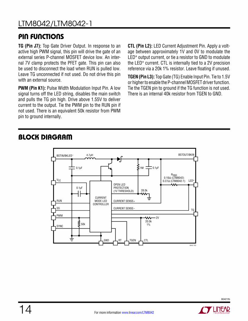
50k
PIN FUNCTIONSTG (Pin J7): Top Gate Driver Output. In response to an active high PWM signal, this pin will drive the gate of an external series P-channel MOSFET device low. An inter-nal 7V clamp protects the PFET gate. This pin can also be used to disconnect the load when RUN is pulled low. Leave TG unconnected if not used. Do not drive this pin with an external source.
PWM (Pin K1): Pulse Width Modulation Input Pin. A low signal turns off the LED string, disables the main switch and pulls the TG pin high. Drive above 1.55V to deliver current to the output. Tie the PWM pin to the RUN pin if not used. There is an equivalent 50k resistor from PWM pin to ground internally.
CTL (Pin L2): LED Current Adjustment Pin. Apply a volt-age between approximately 1V and 0V to modulate the LED+ output current, or tie a resistor to GND to modulate the LED+ current. CTL is internally tied to a 2V precision reference via a 20k 1% resistor. Leave floating if unused.
TGEN (Pin L3): Top Gate (TG) Enable Input Pin. Tie to 1.5V or higher to enable the P-channel MOSFET driver function. Tie the TGEN pin to ground if the TG function is not used. There is an internal 40k resistor from TGEN to GND.

LTM8042/LTM8042-1
1580421fb
For more information www.linear.com/LTM8042
OPERATIONThe LTM8042/LTM8042-1 is a complete, full featured, current mode regulator specifically designed to drive light emitting diodes (LEDs) or other loads where a constant current up to 1A (350mA for the LTM8042-1) is required.
The LTM8042/LTM8042-1 can operate in any of three LED drive topologies: boost, buck mode and buck-boost mode. The device features both analog and PWM dimming, a PWM P-channel MOSFET driver, and a suite of control functions: RUN control, soft-start, user programmable switching frequency, and external frequency synchronization.
Operation can be best understood by referring to the Block Diagram. The power stage is a boost converter that regulates the output current by reading the voltage across a power sense resistor that is in series with the output.
As with any boost topology, there is an uninterrupted cur-rent path between the input and output terminals. Current between these two terminals is not limited, so the device is intolerant to a short-circuit or overload from any of the output terminals (LED+, BSTOUT/BKIN) to GND.
There are two ways to dim a LED with the LTM8042/LTM8042-1. One way is to adjust the current on the LED array by setting the analog voltage on the CTL pin. The CTL pin is internally pulled up to a precision 2V reference through a 1% 20k resistor. Leaving the CTL pin floating sets the LED pin current to 1A. Reducing the voltage below 1.1V on the CTL pin proportionally reduces the current flowing out of LED+. This can be accomplished by con-necting a resistor from the CTL pin to GND, forming a divider network with the internal 20k resistor, or by driving the CTL pin directly to a voltage source, such as a DAC.
The other way the LTM8042/LTM8042-1 can dim a LED array is by pulse width modulation using the PWM pin and an optional external P-channel MOSFET. The external P-channel MOSFET can be conveniently operated by the integrated gate driver at pin TG. The gate drive function can be enabled or disabled by the TGEN pin.
If the PWM pin is pulled high, the part operates normally. If the PWM pin is unconnected or pulled low, the LTM8042/LTM8042-1 stops switching and the internal control cir-cuitry is held in its present state. This way, the LTM8042/LTM8042-1 “remembers” the current sourced from the LED+ output until PWM is pulled high again. This leads to a highly linear relationship between pulse width and output light, allowing for a large and accurate dimming range.
The RUN pin is used to deactivate the LTM8042/LTM8042-1. When the RUN pin is pulled to a logic low state, the device is shut down and draws typically less than 1µA of current.
The SS pin is used to limit inrush current during start-up. The LTM8042/LTM8042-1 integrates a current source with this function, so only a capacitor is necessary to establish the soft-start characteristics of the output current.
The switching frequency is set by applying a single resistor from the RT pin to GND, allowing operation anywhere from 250kHz to 2MHz, and the SYNC pin allows synchroniza-tion to an external source between 300kHz and 2.5MHz.
LTM8042/LTM8042-1
1680421fb
For more information www.linear.com/LTM8042
APPLICATIONS INFORMATIONFor most applications, the design process is straight forward, summarized as follows:
1. Decide whether the LTM8042/LTM8042-1 should oper-ate in boost, buck, or buck-boost mode.
2. Look at Tables 1 through 6 and find the line that best matches the input and output conditions of the system under consideration.
3. Connect CIN, COUT, CVCC and RT as indicated in the appropriate table.
4. Connect the remaining pins as needed by the system requirements.
While these component combinations have been tested for proper operation, it is incumbent upon the user to verify proper operation over the intended system’s line, load and environmental conditions.
If the desired LED current is not listed in Tables 1 through 6, set it by applying the proper voltage the CTL pin. Graphs of the LTM8042/LTM8042-1 LED current scaling vs CTL voltage are given in the Typical Performance Character-istics section. If a voltage source is not available to drive the CTL pin, a resistor may be applied from the CTL pin to GND. The CTL pin is internally pulled up to a 2V refer-ence voltage through a 20k resistor (please see the Block Diagram for details).
Open LED Protection
The LTM8042/LTM8042-1 has internal open LED circuit protection. If the LED is absent or fails open, the LTM8042/LTM8042-1 clamps the voltage on the LED+ and BSTOUT/BKIN pin to protect the output against overvoltage. The internal boost switching converter then regulates its output to 36V. In buck mode, the full open LED voltage is stood off by the internal power Schottky diode. At high operating temperatures, the power Schottky reverse leak-age current will rise. This increases the power dissipation within the diode, which raises the junction temperature. This temperature rise can be large, so care needs to be taken at high operating temperatures.
Setting the Switching Frequency
The LTM8042/LTM8042-1 uses a constant frequency architecture that can be programmed over a 250kHz to 2MHz range with a single external timing resistor from the RT pin to ground. Table 7 shows suggested RT selections for a variety of switching frequencies.
Table 7. Switching Frequency vs RT
SWITCHING FREQUENCY (kHz) RT (kΩ)
250 86.6
500 37.4
800 21.0
1000 15.8
1500 9.09
2000 6.04
The other way to set the operating frequency of the LTM8042/LTM8042-1 is to drive the SYNC pin with an external signal. For proper operation, a resistor should be connected at the RT pin and be able to generate a switch-ing frequency 20% lower than the external clock when the external clock is absent.
In general, a lower switching frequency should be used where either very high or very low switching duty cycle operation is required, or high efficiency is desired. Selection of a higher switching frequency will allow use of smaller value external components and yield a smaller solution size and profile.
Operating Modes
The LTM8042/LTM8042-1 employs a ground referred power switch to implement a boost power switching circuit. As such, it can be used to implement the three most popular LED driving topologies: boost, buck mode, and buck-boost mode. Example layouts of each operating mode are given in Figures 2 through 4 and schematics are shown in the Typical Applications section.
LTM8042/LTM8042-1
1780421fb
For more information www.linear.com/LTM8042
APPLICATIONS INFORMATIONWhich mode to use depends upon the operating condi-tions. Boost is generally selected when the voltage across the LED string is always higher than the input voltage. Buck mode is the dual of boost, used when the voltage across the LED string is always lower than VIN. Finally, buck-boost mode is used when the VIN can vary both above and below the voltage across the LED string.
The land grid array of the LTM8042/LTM8042-1 is designed to conveniently accommodate all three operating modes. Please refer to the PCB Layout section for suggested examples of how to lay out each operating mode.
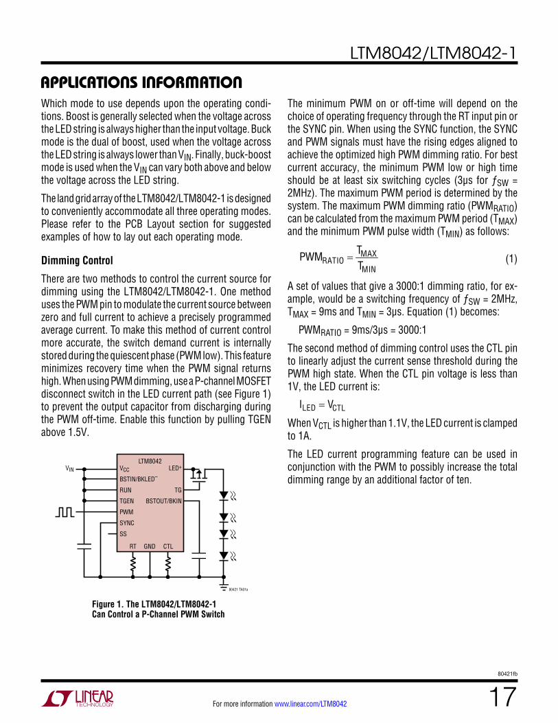
Dimming Control
There are two methods to control the current source for dimming using the LTM8042/LTM8042-1. One method uses the PWM pin to modulate the current source between zero and full current to achieve a precisely programmed average current. To make this method of current control more accurate, the switch demand current is internally stored during the quiescent phase (PWM low). This feature minimizes recovery time when the PWM signal returns high. When using PWM dimming, use a P-channel MOSFET disconnect switch in the LED current path (see Figure 1) to prevent the output capacitor from discharging during the PWM off-time. Enable this function by pulling TGEN above 1.5V.
Figure 1. The LTM8042/LTM8042-1 Can Control a P-Channel PWM Switch
The minimum PWM on or off-time will depend on the choice of operating frequency through the RT input pin or the SYNC pin. When using the SYNC function, the SYNC and PWM signals must have the rising edges aligned to achieve the optimized high PWM dimming ratio. For best current accuracy, the minimum PWM low or high time should be at least six switching cycles (3μs for ƒSW = 2MHz). The maximum PWM period is determined by the system. The maximum PWM dimming ratio (PWMRATIO) can be calculated from the maximum PWM period (TMAX) and the minimum PWM pulse width (TMIN) as follows:
PWMRATIO =
TMAX
TMIN (1)
A set of values that give a 3000:1 dimming ratio, for ex-ample, would be a switching frequency of ƒSW = 2MHz, TMAX = 9ms and TMIN = 3μs. Equation (1) becomes:
PWMRATIO = 9ms/3μs = 3000:1
The second method of dimming control uses the CTL pin to linearly adjust the current sense threshold during the PWM high state. When the CTL pin voltage is less than 1V, the LED current is:
ILED = VCTL
When VCTL is higher than 1.1V, the LED current is clamped to 1A.
The LED current programming feature can be used in conjunction with the PWM to possibly increase the total dimming range by an additional factor of ten.
80421 TA01a
LTM8042
RT GND CTL
VCC
BSTIN/BKLED–
RUN
TGEN
PWM
SYNC
SS
VIN LED+
TG
BSTOUT/BKIN
LTM8042/LTM8042-1
1880421fb
For more information www.linear.com/LTM8042
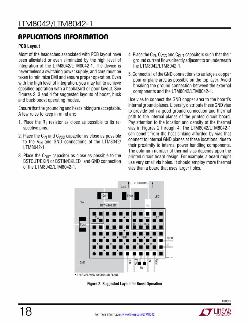
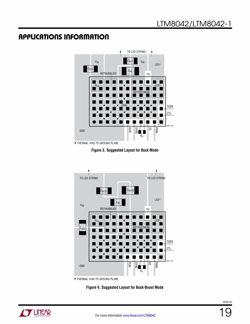
APPLICATIONS INFORMATIONPCB Layout
Most of the headaches associated with PCB layout have been alleviated or even eliminated by the high level of integration of the LTM8042/LTM8042-1. The device is nevertheless a switching power supply, and care must be taken to minimize EMI and ensure proper operation. Even with the high level of integration, you may fail to achieve specified operation with a haphazard or poor layout. See Figures 2, 3 and 4 for suggested layouts of boost, buck and buck-boost operating modes.
Ensure that the grounding and heat sinking are acceptable. A few rules to keep in mind are:
1. Place the RT resistor as close as possible to its re-spective pins.
2. Place the CIN and CVCC capacitor as close as possible to the VIN and GND connections of the LTM8042/LTM8042-1.
3. Place the COUT capacitor as close as possible to the BSTOUT/BKIN or BSTIN/BKLED– and GND connection of the LTM8042/LTM8042-1.
BSTOUT/BKIN
BSTIN/BKLED–
LED+
LED+
GND
VIN
RUN
SYNC
RT
SS PWM
TGEN
80421 F02
TG
TO LED STRING
CTL
VCC
CVCC
CIN COUT
THERMAL VIAS TO GROUND PLANE
GND
GND
Figure 2. Suggested Layout for Boost Operation
4. Place the CIN, CVCC and COUT capacitors such that their ground current flows directly adjacent to or underneath the LTM8042/LTM8042-1.
5. Connect all of the GND connections to as large a copper pour or plane area as possible on the top layer. Avoid breaking the ground connection between the external components and the LTM8042/LTM8042-1.
Use vias to connect the GND copper area to the board’s internal ground planes. Liberally distribute these GND vias to provide both a good ground connection and thermal path to the internal planes of the printed circuit board. Pay attention to the location and density of the thermal vias in Figures 2 through 4. The LTM8042/LTM8042-1 can benefit from the heat sinking afforded by vias that connect to internal GND planes at these locations, due to their proximity to internal power handling components. The optimum number of thermal vias depends upon the printed circuit board design. For example, a board might use very small via holes. It should employ more thermal vias than a board that uses larger holes.
LTM8042/LTM8042-1
1980421fb
For more information www.linear.com/LTM8042
APPLICATIONS INFORMATION
Figure 3. Suggested Layout for Buck Mode
Figure 4. Suggested Layout for Buck-Boost Mode
BSTOUT/BKIN
LED+
LED+
GND
RUN
SYNC
RT
SS PWM
TGEN
80421 F03
TG
CTL
VCC
CVCC CIN
VINVINCOUT
THERMAL VIAS TO GROUND PLANE
BSTIN/BKLED–
GND
TO LED STRING
BSTOUT/BKIN
LED+
LED+
GND
VIN
RUN
SYNC
RT
SS PWM
TGEN
80421 F04
TG
CTL
VCC
CVCC
COUT1
CIN
COUT2
THERMAL VIAS TO GROUND PLANE
TO LED STRING TO LED STRING
BSTIN/BKLED–
LTM8042/LTM8042-1
2080421fb
For more information www.linear.com/LTM8042
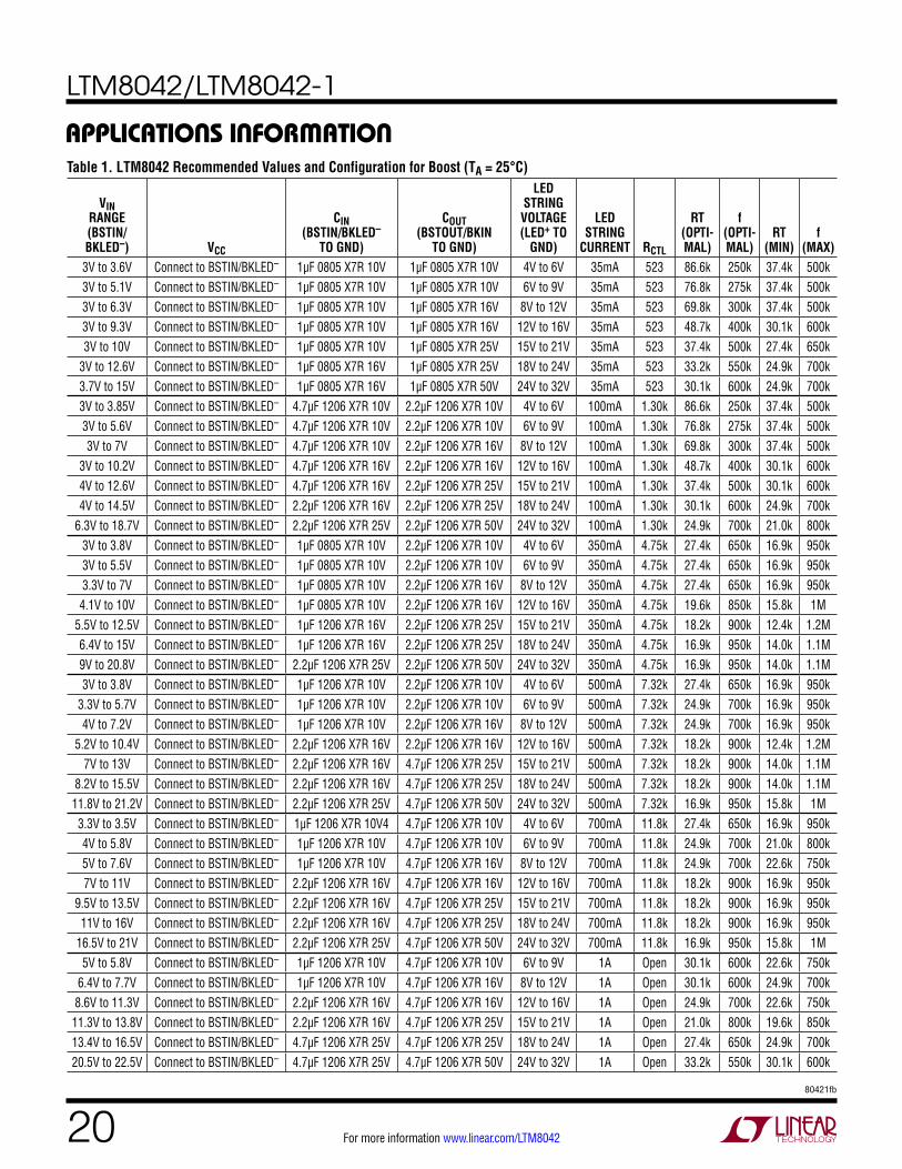
APPLICATIONS INFORMATIONTable 1. LTM8042 Recommended Values and Configuration for Boost (TA = 25°C)
VIN RANGE (BSTIN/BKLED–) VCC
CIN (BSTIN/BKLED–
TO GND)
COUT (BSTOUT/BKIN
TO GND)
LED STRING VOLTAGE (LED+ TO
GND)
LED STRING
CURRENT RCTL
RT (OPTI-MAL)
f (OPTI-MAL)
RT (MIN)
f (MAX)
3V to 3.6V Connect to BSTIN/BKLED– 1µF 0805 X7R 10V 1µF 0805 X7R 10V 4V to 6V 35mA 523 86.6k 250k 37.4k 500k3V to 5.1V Connect to BSTIN/BKLED– 1µF 0805 X7R 10V 1µF 0805 X7R 10V 6V to 9V 35mA 523 76.8k 275k 37.4k 500k3V to 6.3V Connect to BSTIN/BKLED– 1µF 0805 X7R 10V 1µF 0805 X7R 16V 8V to 12V 35mA 523 69.8k 300k 37.4k 500k3V to 9.3V Connect to BSTIN/BKLED– 1µF 0805 X7R 10V 1µF 0805 X7R 16V 12V to 16V 35mA 523 48.7k 400k 30.1k 600k3V to 10V Connect to BSTIN/BKLED– 1µF 0805 X7R 10V 1µF 0805 X7R 25V 15V to 21V 35mA 523 37.4k 500k 27.4k 650k
3V to 12.6V Connect to BSTIN/BKLED– 1µF 0805 X7R 16V 1µF 0805 X7R 25V 18V to 24V 35mA 523 33.2k 550k 24.9k 700k3.7V to 15V Connect to BSTIN/BKLED– 1µF 0805 X7R 16V 1µF 0805 X7R 50V 24V to 32V 35mA 523 30.1k 600k 24.9k 700k3V to 3.85V Connect to BSTIN/BKLED– 4.7µF 1206 X7R 10V 2.2µF 1206 X7R 10V 4V to 6V 100mA 1.30k 86.6k 250k 37.4k 500k3V to 5.6V Connect to BSTIN/BKLED– 4.7µF 1206 X7R 10V 2.2µF 1206 X7R 10V 6V to 9V 100mA 1.30k 76.8k 275k 37.4k 500k3V to 7V Connect to BSTIN/BKLED– 4.7µF 1206 X7R 10V 2.2µF 1206 X7R 16V 8V to 12V 100mA 1.30k 69.8k 300k 37.4k 500k
3V to 10.2V Connect to BSTIN/BKLED– 4.7µF 1206 X7R 16V 2.2µF 1206 X7R 16V 12V to 16V 100mA 1.30k 48.7k 400k 30.1k 600k4V to 12.6V Connect to BSTIN/BKLED– 4.7µF 1206 X7R 16V 2.2µF 1206 X7R 25V 15V to 21V 100mA 1.30k 37.4k 500k 30.1k 600k4V to 14.5V Connect to BSTIN/BKLED– 2.2µF 1206 X7R 16V 2.2µF 1206 X7R 25V 18V to 24V 100mA 1.30k 30.1k 600k 24.9k 700k
6.3V to 18.7V Connect to BSTIN/BKLED– 2.2µF 1206 X7R 25V 2.2µF 1206 X7R 50V 24V to 32V 100mA 1.30k 24.9k 700k 21.0k 800k3V to 3.8V Connect to BSTIN/BKLED– 1µF 0805 X7R 10V 2.2µF 1206 X7R 10V 4V to 6V 350mA 4.75k 27.4k 650k 16.9k 950k3V to 5.5V Connect to BSTIN/BKLED– 1µF 0805 X7R 10V 2.2µF 1206 X7R 10V 6V to 9V 350mA 4.75k 27.4k 650k 16.9k 950k3.3V to 7V Connect to BSTIN/BKLED– 1µF 0805 X7R 10V 2.2µF 1206 X7R 16V 8V to 12V 350mA 4.75k 27.4k 650k 16.9k 950k4.1V to 10V Connect to BSTIN/BKLED– 1µF 0805 X7R 10V 2.2µF 1206 X7R 16V 12V to 16V 350mA 4.75k 19.6k 850k 15.8k 1M
5.5V to 12.5V Connect to BSTIN/BKLED– 1µF 1206 X7R 16V 2.2µF 1206 X7R 25V 15V to 21V 350mA 4.75k 18.2k 900k 12.4k 1.2M6.4V to 15V Connect to BSTIN/BKLED– 1µF 1206 X7R 16V 2.2µF 1206 X7R 25V 18V to 24V 350mA 4.75k 16.9k 950k 14.0k 1.1M9V to 20.8V Connect to BSTIN/BKLED– 2.2µF 1206 X7R 25V 2.2µF 1206 X7R 50V 24V to 32V 350mA 4.75k 16.9k 950k 14.0k 1.1M3V to 3.8V Connect to BSTIN/BKLED– 1µF 1206 X7R 10V 2.2µF 1206 X7R 10V 4V to 6V 500mA 7.32k 27.4k 650k 16.9k 950k
3.3V to 5.7V Connect to BSTIN/BKLED– 1µF 1206 X7R 10V 2.2µF 1206 X7R 10V 6V to 9V 500mA 7.32k 24.9k 700k 16.9k 950k4V to 7.2V Connect to BSTIN/BKLED– 1µF 1206 X7R 10V 2.2µF 1206 X7R 16V 8V to 12V 500mA 7.32k 24.9k 700k 16.9k 950k
5.2V to 10.4V Connect to BSTIN/BKLED– 2.2µF 1206 X7R 16V 2.2µF 1206 X7R 16V 12V to 16V 500mA 7.32k 18.2k 900k 12.4k 1.2M7V to 13V Connect to BSTIN/BKLED– 2.2µF 1206 X7R 16V 4.7µF 1206 X7R 25V 15V to 21V 500mA 7.32k 18.2k 900k 14.0k 1.1M
8.2V to 15.5V Connect to BSTIN/BKLED– 2.2µF 1206 X7R 16V 4.7µF 1206 X7R 25V 18V to 24V 500mA 7.32k 18.2k 900k 14.0k 1.1M11.8V to 21.2V Connect to BSTIN/BKLED– 2.2µF 1206 X7R 25V 4.7µF 1206 X7R 50V 24V to 32V 500mA 7.32k 16.9k 950k 15.8k 1M3.3V to 3.5V Connect to BSTIN/BKLED– 1µF 1206 X7R 10V4 4.7µF 1206 X7R 10V 4V to 6V 700mA 11.8k 27.4k 650k 16.9k 950k4V to 5.8V Connect to BSTIN/BKLED– 1µF 1206 X7R 10V 4.7µF 1206 X7R 10V 6V to 9V 700mA 11.8k 24.9k 700k 21.0k 800k5V to 7.6V Connect to BSTIN/BKLED– 1µF 1206 X7R 10V 4.7µF 1206 X7R 16V 8V to 12V 700mA 11.8k 24.9k 700k 22.6k 750k7V to 11V Connect to BSTIN/BKLED– 2.2µF 1206 X7R 16V 4.7µF 1206 X7R 16V 12V to 16V 700mA 11.8k 18.2k 900k 16.9k 950k
9.5V to 13.5V Connect to BSTIN/BKLED– 2.2µF 1206 X7R 16V 4.7µF 1206 X7R 25V 15V to 21V 700mA 11.8k 18.2k 900k 16.9k 950k11V to 16V Connect to BSTIN/BKLED– 2.2µF 1206 X7R 16V 4.7µF 1206 X7R 25V 18V to 24V 700mA 11.8k 18.2k 900k 16.9k 950k
16.5V to 21V Connect to BSTIN/BKLED– 2.2µF 1206 X7R 25V 4.7µF 1206 X7R 50V 24V to 32V 700mA 11.8k 16.9k 950k 15.8k 1M5V to 5.8V Connect to BSTIN/BKLED– 1µF 1206 X7R 10V 4.7µF 1206 X7R 10V 6V to 9V 1A Open 30.1k 600k 22.6k 750k
6.4V to 7.7V Connect to BSTIN/BKLED– 1µF 1206 X7R 10V 4.7µF 1206 X7R 16V 8V to 12V 1A Open 30.1k 600k 24.9k 700k8.6V to 11.3V Connect to BSTIN/BKLED– 2.2µF 1206 X7R 16V 4.7µF 1206 X7R 16V 12V to 16V 1A Open 24.9k 700k 22.6k 750k
11.3V to 13.8V Connect to BSTIN/BKLED– 2.2µF 1206 X7R 16V 4.7µF 1206 X7R 25V 15V to 21V 1A Open 21.0k 800k 19.6k 850k13.4V to 16.5V Connect to BSTIN/BKLED– 4.7µF 1206 X7R 25V 4.7µF 1206 X7R 25V 18V to 24V 1A Open 27.4k 650k 24.9k 700k20.5V to 22.5V Connect to BSTIN/BKLED– 4.7µF 1206 X7R 25V 4.7µF 1206 X7R 50V 24V to 32V 1A Open 33.2k 550k 30.1k 600k

LTM8042/LTM8042-1
2180421fb
For more information www.linear.com/LTM8042
APPLICATIONS INFORMATIONTable 2. LTM8042 Recommended Values and Configuration for Buck Mode (TA = 25°C)
VIN RANGE (BSTOUT/BKIN) VCC CVCC
CIN (BSTOUT/BKIN
TO GND)
COUT (BSTOUT/BKIN TO
BSTIN/BKLED–)
LED STRING VOLTAGE (LED+ TO BSTIN/
BKLED–)
LED STRING
CURRENT RCTL
RT (OPTI-MAL)
f (OPTI-MAL)
RT (MIN)
f (MAX)
4.4V to 5.5V 3V to 30V 1µF 0805 X7R 50V 1µF 1206 X7R 50V 2.2µF 1206 X7R 10V 2V to 4V 35mA 523 86.6k 250k 86.6k 250k
6.8V to 14V 3V to 30V 1µF 0805 X7R 50V 1µF 1206 X7R 50V 2.2µF 1206 X7R 10V 4V to 6V 35mA 523 86.6k 250k 86.6k 250k
9.6V to 26V 3V to 30V 1µF 0805 X7R 50V 1µF 1206 X7R 50V 2.2µF 1206 X7R 16V 6V to 9V 35mA 523 86.6k 250k 86.6k 250k
12.5V to 33V 3V to 30V 1µF 0805 X7R 50V 1µF 1206 X7R 50V 2.2µF 1210 X7R 16V 8V to 12V 35mA 523 86.6k 250k 86.6k 250k
16.6V to 33V 3V to 30V 1µF 0805 X7R 50V 1µF 1206 X7R 50V 2.2µF 1210 X7R 25V 12V to 16V 35mA 523 86.6k 250k 46.4k 420k
21.8V to 33V 3V to 30V 1µF 0805 X7R 50V 1µF 1206 X7R 50V 2.2µF 1210 X7R 25V 15V to 21V 35mA 523 86.6k 250k 33.2k 550k
24.5V to 33V 3V to 30V 1µF 0805 X7R 50V 1µF 1206 X7R 50V 2.2µF 1210 X7R 25V 18V to 24V 35mA 523 86.6k 250k 26.1k 670k
4.5V to 21V 3V to 30V 1µF 0805 X7R 50V 1µF 1206 X7R 50V 4.7µF 1206 X7R 10V 2V to 4V 100mA 1.30k 86.6k 250k 86.6k 250k
6.8V to 33.8V 3V to 30V 1µF 0805 X7R 50V 1µF 1206 X7R 50V 4.7µF 1206 X7R 10V 4V to 6V 100mA 1.30k 86.6k 250k 86.6k 250k
9.9V to 33.5V 3V to 30V 1µF 0805 X7R 50V 1µF 1206 X7R 50V 4.7µF 1210 X7R 16V 6V to 9V 100mA 1.30k 76.8k 275k 69.8k 300k
13V to 33.4V 3V to 30V 1µF 0805 X7R 50V 1µF 1206 X7R 50V 4.7µF 1210 X7R 16V 8V to 12V 100mA 1.30k 69.8k 300k 48.7k 400k
17.2V to 33.1V 3V to 30V 1µF 0805 X7R 50V 1µF 1206 X7R 50V 4.7µF 1210 X7R 25V 12V to 16V 100mA 1.30k 37.4k 500k 31.6k 575k
23V to 33V 3V to 30V 1µF 0805 X7R 50V 1µF 1206 X7R 50V 4.7µF 1210 X7R 25V 15V to 21V 100mA 1.30k 24.9k 700k 19.1k 870k
26V to 33V 3V to 30V 1µF 0805 X7R 50V 1µF 1206 X7R 50V 4.7µF 1210 X7R 25V 18V to 24V 100mA 1.30k 21.0k 800k 12.4k 1.2M
5.2V to 33.6V 3V to 30V 1µF 0805 X7R 50V 1µF 1206 X7R 50V 4.7µF 1206 X7R 10V 2V to 4V 350mA 4.75k 61.9k 330k 54.9k 365k
7V to 33.4V 3V to 30V 1µF 0805 X7R 50V 1µF 1206 X7R 50V 4.7µF 1206 X7R 10V 4V to 6V 350mA 4.75k 30.1k 600k 24.9k 700k
10.5V to 33.3V 3V to 30V 1µF 0805 X7R 50V 1µF 1206 X7R 50V 4.7µF 1210 X7R 16V 6V to 9V 350mA 4.75k 21.0k 800k 15.8k 1M
14.5V to 33.2V 3V to 30V 1µF 0805 X7R 50V 1µF 1206 X7R 50V 4.7µF 1210 X7R 16V 8V to 12V 350mA 4.75k 12.4k 1.2M 8.25k 1.6M
19.2V to 33V 3V to 30V 1µF 0805 X7R 50V 1µF 1206 X7R 50V 4.7µF 1210 X7R 25V 12V to 16V 350mA 4.75k 11.0k 1.3M 3.74k 2.5M
25V to 33V 3V to 30V 1µF 0805 X7R 50V 1µF 1206 X7R 50V 4.7µF 1210 X7R 25V 15V to 21V 350mA 4.75k 11.0k 1.3M 3.74k 2.5M
4.9V to 33V 3V to 30V 1µF 0805 X7R 50V 1µF 1206 X7R 50V 4.7µF 1206 X7R 10V 2V to 4V 500mA 7.32k 37.4k 500k 33.2k 550k
7.3V to 33.2V 3V to 30V 1µF 0805 X7R 50V 1µF 1206 X7R 50V 4.7µF 1206 X7R 10V 4V to 6V 500mA 7.32k 21.0k 800k 18.2k 900k
10.7V to 33V 3V to 30V 1µF 0805 X7R 50V 1µF 1206 X7R 50V 4.7µF 1210 X7R 16V 6V to 9V 500mA 7.32k 15.8k 1M 11.0k 1.3M
14.1V to 32.8V 3V to 30V 1µF 0805 X7R 50V 1µF 1206 X7R 50V 4.7µF 1210 X7R 16V 8V to 12V 500mA 7.32k 15.8k 1M 7.50k 1.7M
18.5V to 32.5V 3V to 30V 1µF 0805 X7R 50V 1µF 1206 X7R 50V 4.7µF 1210 X7R 25V 12V to 16V 500mA 7.32k 15.8k 1M 3.74 2.5M
24.3V to 32.5V 3V to 30V 1µF 0805 X7R 50V 1µF 1206 X7R 50V 4.7µF 1210 X7R 25V 15V to 21V 500mA 7.32k 15.8k 1M 3.74k 2.5M
5V to 33.2V 3V to 30V 1µF 0805 X7R 50V 1µF 1206 X7R 50V 4.7µF 1206 X7R 10V 2V to 4V 700mA 11.8k 33.2k 550k 30.1k 600k
7.3V to 32.7V 3V to 30V 1µF 0805 X7R 50V 1µF 1206 X7R 50V 4.7µF 1206 X7R 10V 4V to 6V 700mA 11.8k 21.0k 800k 18.2k 900k
10.8V to 32.7V 3V to 30V 1µF 0805 X7R 50V 1µF 1206 X7R 50V 4.7µF 1210 X7R 16V 6V to 9V 700mA 11.8k 15.8k 1M 11.0k 1.3M
14.4V to 32.2V 3V to 30V 1µF 0805 X7R 50V 1µF 1206 X7R 50V 4.7µF 1210 X7R 16V 8V to 12V 700mA 11.8k 15.8k 1M 7.50k 1.7M
18.8V to 31.7V 3V to 30V 1µF 0805 X7R 50V 1µF 1206 X7R 50V 4.7µF 1210 X7R 25V 12V to 16V 700mA 11.8k 15.8k 1M 3.74k 2.5M
24.3V to 31.8V 3V to 30V 1µF 0805 X7R 50V 1µF 1206 X7R 50V 4.7µF 1210 X7R 25V 15V to 21V 700mA 11.8k 15.8k 1M 3.74k 2.5M
5V to 32V 3V to 30V 1µF 0805 X7R 50V 2.2µF 1206 X7R 50V 4.7µF 1206 X7R 10V 2V to 4V 1A Open 33.2k 550k 30.1k 600k
7.2V to 32V 3V to 30V 1µF 0805 X7R 50V 2.2µF 1206 X7R 50V 4.7µF 1206 X7R 10V 4V to 6V 1A Open 21.0k 800k 16.9k 950k
10.8V to 31V 3V to 30V 1µF 0805 X7R 50V 2.2µF 1206 X7R 50V 4.7µF 1210 X7R 16V 6V to 9V 1A Open 15.8k 1M 11.0k 1.3M
14.3V to 30.5V 3V to 30V 1µF 0805 X7R 50V 2.2µF 1206 X7R 50V 4.7µF 1210 X7R 16V 8V to 12V 1A Open 15.8k 1M 7.50k 1.7M
18.9V to 30.5V 3V to 30V 1µF 0805 X7R 50V 2.2µF 1206 X7R 50V 4.7µF 1210 X7R 25V 12V to 16V 1A Open 15.8k 1M 3.74k 2.5M
24.6V to 30.5V 3V to 30V 1µF 0805 X7R 50V 2.2µF 1206 X7R 50V 4.7µF 1210 X7R 25V 15V to 21V 1A Open 15.8k 1M 3.74k 2.5M

LTM8042/LTM8042-1
2280421fb
For more information www.linear.com/LTM8042
APPLICATIONS INFORMATIONTable 3. LTM8042 Recommended Values and Configuration for Buck-Boost Mode (TA = 25°C)
VIN RANGE (BSTIN/BKLED–) VCC
CVCC (VCC to GND)
CIN (BSTIN/BKLED–
TO GND)
COUT1 (BSTOUT/BKIN
TO BSTIN/BKLED–)
COUT2 (BSTOUT/BKIN
TO GND)
LED STRING VOLTAGE (LED+ to BSTIN/
BKLED–)
LED STRING CURR-
ENT RCTL
RT (OPTI-MAL)
f (OPTI-MAL)
RT (MIN)
f (MAX)
3V to 6V 3V to 30V 1µF 0805 X7R 50V 1µF 0805 X7R 10V 1µF 0805 X7R 10V 1µF 0805 X7R 10V 2V to 4V 35mA 523 86.6k 250k 86.6k 250k
3V to 14V 3V to 30V 1µF 0805 X7R 50V 1µF 0805 X7R 16V 1µF 0805 X7R 10V 1µF 0805 X7R 10V 4V to 6V 35mA 523 86.6k 250k 86.6k 250k
3V to 20V 3V to 30V 1µF 0805 X7R 50V 1µF 1206 X7R 25V 1µF 0805 X7R 10V 1µF 0805 X7R 10V 6V to 9V 35mA 523 86.6k 250k 86.6k 250k
3V to 21V 3V to 30V 1µF 0805 X7R 50V 1µF 1206 X7R 25V 1µF 0805 X7R 16V 1µF 0805 X7R 16V 8V to 12V 35mA 523 86.6k 250k 57.6k 350k
3V to 17.8V 3V to 30V 1µF 0805 X7R 50V 1µF 1206 X7R 25V 1µF 0805 X7R 16V 1µF 1206 X7R 25V 12V to 16V 35mA 523 48.7k 400k 27.4k 650k
3V to 13V 3V to 30V 1µF 0805 X7R 50V 1µF 0805 X7R 16V 1µF 1206 X7R 25V 1µF 1206 X7R 25V 15V to 21V 35mA 523 37.4k 500k 10.0k 1.4M
3.5V to 10.1V 3V to 30V 1µF 0805 X7R 50V 1µF 0805 X7R 16V 1µF 1206 X7R 25V 1µF 1206 X7R 25V 18V to 24V 35mA 523 22.6k 750k 3.74k 2.5M
3V to 21V 3V to 30V 1µF 0805 X7R 50V 1µF 1206 X7R 25V 2.2µF 1206 X7R 10V 1µF 0805 X7R 10V 2V to 4V 100mA 1.30k 86.6k 250k 69.8k 300k
3V to 22.8V 3V to 30V 1µF 0805 X7R 50V 1µF 1206 X7R 25V 1µF 0805 X7R 10V 1µF 0805 X7R 10V 4V to 6V 100mA 1.30k 48.7k 400k 43.2k 450k
3V to 23.4V 3V to 30V 1µF 0805 X7R 50V 1µF 1206 X7R 25V 1µF 0805 X7R 10V 1µF 0805 X7R 10V 6V to 9V 100mA 1.30k 37.4k 500k 30.1k 600k
3V to 21.8V 3V to 30V 1µF 0805 X7R 50V 1µF 1206 X7R 25V 1µF 0805 X7R 16V 1µF 1206 X7R 25V 8V to 12V 100mA 1.30k 21.0k 800k 16.9k 950k
3V to 17.9V 3V to 30V 1µF 0805 X7R 50V 1µF 1206 X7R 25V 1µF 0805 X7R 16V 1µF 1206 X7R 25V 12V to 16V 100mA 1.30k 19.6k 850k 11.0k 1.3M
3V to 12.6V 3V to 30V 1µF 0805 X7R 50V 1µF 0805 X7R 16V 1µF 1206 X7R 25V 1µF 1206 X7R 25V 15V to 21V 100mA 1.30k 19.6k 850k 4.02k 2.4M
3.7V to 9.7V 3V to 30V 1µF 0805 X7R 50V 1µF 0805 X7R 10V 1µF 1206 X7R 25V 1µF 1206 X7R 25V 18V to 24V 100mA 1.30k 19.6k 850k 3.74k 2.5M
3V to 28V 3V to 30V 1µF 0805 X7R 50V 1µF 1206 X7R 50V 2.2µF 1206 X7R 10V 1µF 0805 X7R 10V 2V to 4V 350mA 4.75k 43.2k 450k 37.4k 500k
3V to 27.5V 3V to 30V 1µF 0805 X7R 50V 1µF 1206 X7R 50V 2.2µF 1206 X7R 10V 1µF 0805 X7R 10V 4V to 6V 350mA 4.75k 33.2k 550k 24.9k 700k
4.5V to 24.5V 3V to 30V 1µF 0805 X7R 50V 1µF 1206 X7R 25V 2.2µF 1206 X7R 10V 1µF 0805 X7R 10V 6V to 9V 350mA 4.75k 24.9k 700k 10.7k 1.35M
5.5V to 20.7V 3V to 30V 1µF 0805 X7R 50V 1µF 1206 X7R 25V 2.2µF 1206 X7R 16V 1µF 1206 X7R 25V 8V to 12V 350mA 4.75k 15.8k 1M 6.19k 1.9M
7V to 17.1V 3V to 30V 1µF 0805 X7R 50V 1µF 1206 X7R 25V 2.2µF 1206 X7R 16V 1µF 1206 X7R 25V 12V to 16V 350mA 4.75k 15.8k 1M 3.74k 2.5M
8.2V to 11.4V 3V to 30V 1µF 0805 X7R 50V 1µF 0805 X7R 16V 4.7µF 1210 X7R 25V 1µF 1206 X7R 25V 15V to 21V 350mA 4.75k 18.2k 900k 3.74k 2.5M
3V to 23V 3V to 30V 1µF 0805 X7R 50V 1µF 1206 X7R 25V 2.2µF 1206 X7R 10V 1µF 0805 X7R 10V 2V to 4V 500mA 7.32k 27.4k 650k 24.9k 700k
4.5V to 27V 3V to 30V 1µF 0805 X7R 50V 1µF 1206 X7R 50V 2.2µF 1206 X7R 10V 1µF 0805 X7R 10V 4V to 6V 500mA 7.32k 21.0k 800k 19.6k 850k
6V to 24V 3V to 30V 1µF 0805 X7R 50V 1µF 1206 X7R 25V 2.2µF 1206 X7R 10V 1µF 0805 X7R 10V 6V to 9V 500mA 7.32k 15.8k 1M 10.0k 1.4M
7.3V to 20.3V 3V to 30V 1µF 0805 X7R 50V 1µF 1206 X7R 25V 2.2µF 1206 X7R 16V 1µF 1206 X7R 25V 8V to 12V 500mA 7.32k 15.8k 1M 6.34k 1.85M
9.4V to 15V 3V to 30V 1µF 0805 X7R 50V 1µF 0805 X7R 16V 2.2µF 1206 X7R 16V 1µF 1206 X7R 25V 12V to 16V 500mA 7.32k 15.8k 1M 3.74k 2.5M
4.2V to 23.8V 3V to 30V 1µF 0805 X7R 50V 2.2µF 1206 X7R 25V 2.2µF 1206 X7R 10V 1µF 0805 X7R 10V 2V to 4V 700mA 11.8k 24.9k 700k 22.6k 750k
4.7V to 27V 3V to 30V 1µF 0805 X7R 50V 2.2µF 1206 X7R 50V 2.2µF 1206 X7R 10V 1µF 0805 X7R 10V 4V to 6V 700mA 11.8k 16.9k 950k 15.8k 1M
6.1V to 23V 3V to 30V 1µF 0805 X7R 50V 2.2µF 1206 X7R 25V 2.2µF 1206 X7R 10V 1µF 0805 X7R 10V 6V to 9V 700mA 11.8k 16.9k 950k 9.09k 1.5M
7.3V to 20V 3V to 30V 1µF 0805 X7R 50V 2.2µF 1206 X7R 25V 2.2µF 1206 X7R 16V 1µF 1206 X7R 25V 8V to 12V 700mA 11.8k 16.9k 950k 6.19k 1.9M
10.5V to 16.5V 3V to 30V 1µF 0805 X7R 50V 2.2µF 1206 X7R 25V 4.7µF 1210 X7R 16V 1µF 1206 X7R 25V 12V to 16V 700mA 11.8k 15.8k 1M 3.74k 2.5M
4.7V to 28.5V 3V to 30V 1µF 0805 X7R 50V 2.2µF 1206 X7R 50V 4.7µF 1206 X7R 10V 1µF 0805 X7R 10V 2V to 4V 1A Open 24.9k 700k 22.6k 750k
6.7V to 26.8V 3V to 30V 1µF 0805 X7R 50V 2.2µF 1206 X7R 50V 4.7µF 1206 X7R 10V 1µF 0805 X7R 10V 4V to 6V 1A Open 22.6k 750k 16.9k 950k
9V to 23.5V 3V to 30V 1µF 0805 X7R 50V 4.7µF 1210 X7R 25V 4.7µF 1206 X7R 10V 1µF 0805 X7R 10V 6V to 9V 1A Open 22.6k 750k 10.0k 1.4M
13.5V to 20V 3V to 30V 1µF 0805 X7R 50V 4.7µF 1210 X7R 25V 4.7µF 1210 X7R 16V 1µF 1206 X7R 25V 8V to 12V 1A Open 22.6k 750k 5.76k 2M
LTM8042/LTM8042-1
2380421fb
For more information www.linear.com/LTM8042
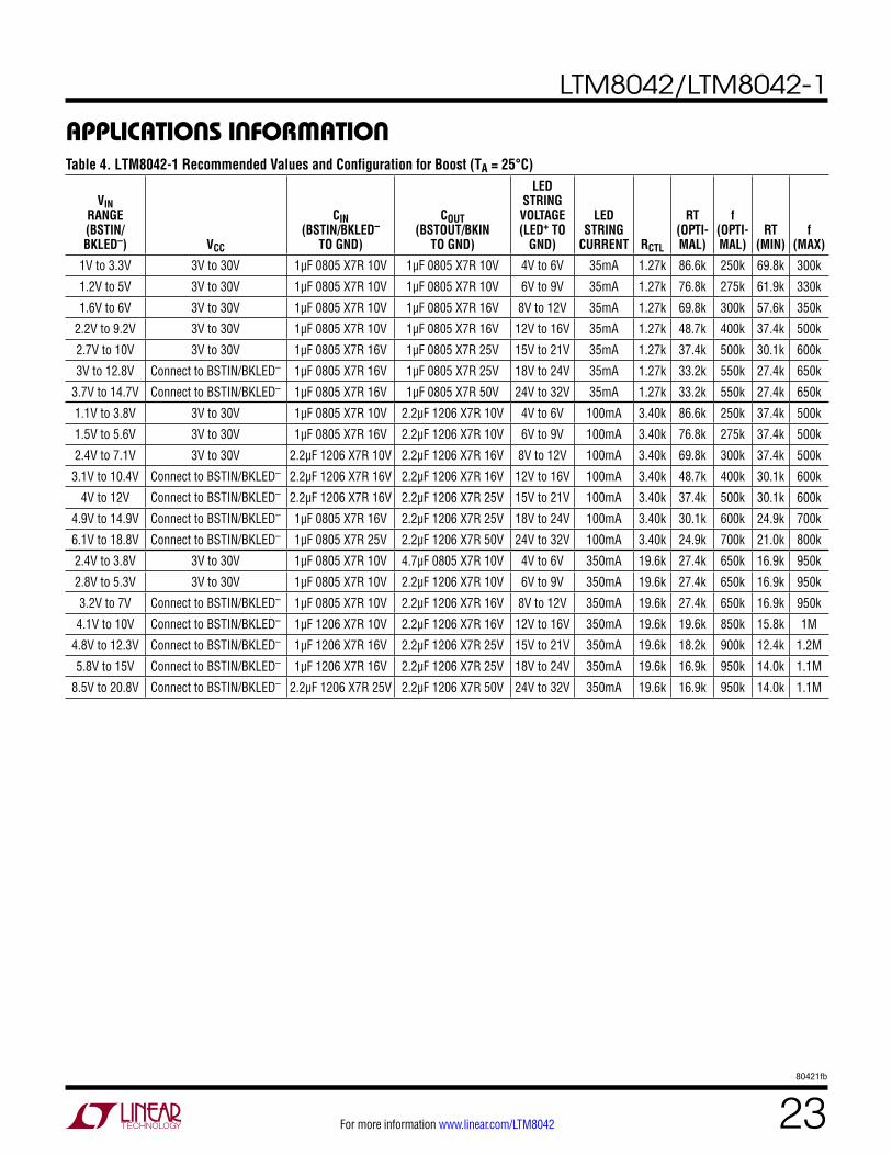
APPLICATIONS INFORMATIONTable 4. LTM8042-1 Recommended Values and Configuration for Boost (TA = 25°C)
VIN RANGE (BSTIN/BKLED–) VCC
CIN (BSTIN/BKLED–
TO GND)
COUT (BSTOUT/BKIN
TO GND)
LED STRING VOLTAGE (LED+ TO
GND)
LED STRING
CURRENT RCTL
RT (OPTI-MAL)
f (OPTI-MAL)
RT (MIN)
f (MAX)
1V to 3.3V 3V to 30V 1µF 0805 X7R 10V 1µF 0805 X7R 10V 4V to 6V 35mA 1.27k 86.6k 250k 69.8k 300k
1.2V to 5V 3V to 30V 1µF 0805 X7R 10V 1µF 0805 X7R 10V 6V to 9V 35mA 1.27k 76.8k 275k 61.9k 330k
1.6V to 6V 3V to 30V 1µF 0805 X7R 10V 1µF 0805 X7R 16V 8V to 12V 35mA 1.27k 69.8k 300k 57.6k 350k
2.2V to 9.2V 3V to 30V 1µF 0805 X7R 10V 1µF 0805 X7R 16V 12V to 16V 35mA 1.27k 48.7k 400k 37.4k 500k
2.7V to 10V 3V to 30V 1µF 0805 X7R 16V 1µF 0805 X7R 25V 15V to 21V 35mA 1.27k 37.4k 500k 30.1k 600k
3V to 12.8V Connect to BSTIN/BKLED– 1µF 0805 X7R 16V 1µF 0805 X7R 25V 18V to 24V 35mA 1.27k 33.2k 550k 27.4k 650k
3.7V to 14.7V Connect to BSTIN/BKLED– 1µF 0805 X7R 16V 1µF 0805 X7R 50V 24V to 32V 35mA 1.27k 33.2k 550k 27.4k 650k
1.1V to 3.8V 3V to 30V 1µF 0805 X7R 10V 2.2µF 1206 X7R 10V 4V to 6V 100mA 3.40k 86.6k 250k 37.4k 500k
1.5V to 5.6V 3V to 30V 1µF 0805 X7R 16V 2.2µF 1206 X7R 10V 6V to 9V 100mA 3.40k 76.8k 275k 37.4k 500k
2.4V to 7.1V 3V to 30V 2.2µF 1206 X7R 10V 2.2µF 1206 X7R 16V 8V to 12V 100mA 3.40k 69.8k 300k 37.4k 500k
3.1V to 10.4V Connect to BSTIN/BKLED– 2.2µF 1206 X7R 16V 2.2µF 1206 X7R 16V 12V to 16V 100mA 3.40k 48.7k 400k 30.1k 600k
4V to 12V Connect to BSTIN/BKLED– 2.2µF 1206 X7R 16V 2.2µF 1206 X7R 25V 15V to 21V 100mA 3.40k 37.4k 500k 30.1k 600k
4.9V to 14.9V Connect to BSTIN/BKLED– 1µF 0805 X7R 16V 2.2µF 1206 X7R 25V 18V to 24V 100mA 3.40k 30.1k 600k 24.9k 700k
6.1V to 18.8V Connect to BSTIN/BKLED– 1µF 0805 X7R 25V 2.2µF 1206 X7R 50V 24V to 32V 100mA 3.40k 24.9k 700k 21.0k 800k
2.4V to 3.8V 3V to 30V 1µF 0805 X7R 10V 4.7µF 0805 X7R 10V 4V to 6V 350mA 19.6k 27.4k 650k 16.9k 950k
2.8V to 5.3V 3V to 30V 1µF 0805 X7R 10V 2.2µF 1206 X7R 10V 6V to 9V 350mA 19.6k 27.4k 650k 16.9k 950k
3.2V to 7V Connect to BSTIN/BKLED– 1µF 0805 X7R 10V 2.2µF 1206 X7R 16V 8V to 12V 350mA 19.6k 27.4k 650k 16.9k 950k
4.1V to 10V Connect to BSTIN/BKLED– 1µF 1206 X7R 10V 2.2µF 1206 X7R 16V 12V to 16V 350mA 19.6k 19.6k 850k 15.8k 1M
4.8V to 12.3V Connect to BSTIN/BKLED– 1µF 1206 X7R 16V 2.2µF 1206 X7R 25V 15V to 21V 350mA 19.6k 18.2k 900k 12.4k 1.2M
5.8V to 15V Connect to BSTIN/BKLED– 1µF 1206 X7R 16V 2.2µF 1206 X7R 25V 18V to 24V 350mA 19.6k 16.9k 950k 14.0k 1.1M
8.5V to 20.8V Connect to BSTIN/BKLED– 2.2µF 1206 X7R 25V 2.2µF 1206 X7R 50V 24V to 32V 350mA 19.6k 16.9k 950k 14.0k 1.1M

LTM8042/LTM8042-1
2480421fb
For more information www.linear.com/LTM8042
APPLICATIONS INFORMATIONTable 5. LTM8042-1 Recommended Values and Configuration for Buck Mode (TA = 25°C)
VIN RANGE (BSTOUT/
BKIN) VCC CVCC
CIN (BSTOUT/BKIN
TO GND)
COUT (BSTOUT/BKIN TO
BSTIN/BKLED–)
LED STRING VOLTAGE (LED+ TO BSTIN/
BKLED–)
LED STRING
CURRENT RCTL
R (OPTI-MAL)
f (OPTI-MAL)
RT (MIN)
f (MAX)
4.3V to 8.3V 3V to 30V 1µF 0805 X7R 50V 1µF 1206 X7R 50V 2.2µF 1206 X7R 10V 2V to 4V 35mA 1.27k 86.6k 250k 86.6k 250k
6.6V to 20V 3V to 30V 1µF 0805 X7R 50V 1µF 1206 X7R 50V 2.2µF 1206 X7R 10V 4V to 6V 35mA 1.27k 86.6k 250k 86.6k 250k
9.5V to 31.5V 3V to 30V 1µF 0805 X7R 50V 1µF 1206 X7R 50V 2.2µF 1206 X7R 16V 6V to 9V 35mA 1.27k 86.6k 250k 86.6k 250k
12.5V to 33V 3V to 30V 1µF 0805 X7R 50V 1µF 1206 X7R 50V 2.2µF 1210 X7R 16V 8V to 12V 35mA 1.27k 86.6k 250k 86.6k 250k
16.6V to 33.2V 3V to 30V 1µF 0805 X7R 50V 1µF 1206 X7R 50V 2.2µF 1210 X7R 25V 12V to 16V 35mA 1.27k 86.6k 250k 46.4k 420k
21.8V to 33.6V 3V to 30V 1µF 0805 X7R 50V 1µF 1206 X7R 50V 2.2µF 1210 X7R 25V 15V to 21V 35mA 1.27k 86.6k 250k 33.2k 550k
24.4V to 33.1V 3V to 30V 1µF 0805 X7R 50V 1µF 1206 X7R 50V 2.2µF 1210 X7R 25V 18V to 24V 35mA 1.27k 86.6k 250k 26.1k 670k
4.3V to 19.5V 3V to 30V 1µF 0805 X7R 50V 1µF 1206 X7R 50V 4.7µF 1206 X7R 10V 2V to 4V 100mA 3.40k 86.6k 250k 86.6k 250k
6.5V to 33.8V 3V to 30V 1µF 0805 X7R 50V 1µF 1206 X7R 50V 4.7µF 1206 X7R 10V 4V to 6V 100mA 3.40k 86.6k 250k 86.6k 250k
9.6V to 34.5V 3V to 30V 1µF 0805 X7R 50V 1µF 1206 X7R 50V 4.7µF 1210 X7R 16V 6V to 9V 100mA 3.40k 76.8k 275k 57.6k 350k
12.6V to 34.4V 3V to 30V 1µF 0805 X7R 50V 1µF 1206 X7R 50V 4.7µF 1210 X7R 16V 8V to 12V 100mA 3.40k 69.8k 300k 48.7k 400k
17V to 34.5V 3V to 30V 1µF 0805 X7R 50V 1µF 1206 X7R 50V 4.7µF 1210 X7R 25V 12V to 16V 100mA 3.40k 37.4k 500k 31.6k 575k
22.8V to 34.5V 3V to 30V 1µF 0805 X7R 50V 1µF 1206 X7R 50V 4.7µF 1210 X7R 25V 15V to 21V 100mA 3.40k 24.9k 700k 19.1k 870k
26.2V to 34.4V 3V to 30V 1µF 0805 X7R 50V 1µF 1206 X7R 50V 4.7µF 1210 X7R 25V 18V to 24V 100mA 3.40k 21.0k 800k 12.4k 1.2M
4.6V to 34.3V 3V to 30V 1µF 0805 X7R 50V 1µF 1206 X7R 50V 4.7µF 1206 X7R 10V 2V to 4V 350mA 19.6k 61.9k 330k 54.9k 365k
6.7V to 34.3V 3V to 30V 1µF 0805 X7R 50V 1µF 1206 X7R 50V 4.7µF 1206 X7R 10V 4V to 6V 350mA 19.6k 30.1k 600k 24.9k 700k
10.3V to 34.3V 3V to 30V 1µF 0805 X7R 50V 1µF 1206 X7R 50V 4.7µF 1210 X7R 16V 6V to 9V 350mA 19.6k 21.0k 800k 15.8k 1M
13.7V to 34.5V 3V to 30V 1µF 0805 X7R 50V 1µF 1206 X7R 50V 4.7µF 1210 X7R 16V 8V to 12V 350mA 19.6k 19.6k 850k 8.25k 1.6M
18.6V to 34.6V 3V to 30V 1µF 0805 X7R 50V 1µF 1206 X7R 50V 4.7µF 1210 X7R 25V 12V to 16V 350mA 19.6k 14.0k 1.1M 3.74k 2.5M
24.1V to 34.3V 3V to 30V 1µF 0805 X7R 50V 1µF 1206 X7R 50V 4.7µF 1210 X7R 25V 15V to 21V 350mA 19.6k 15.8k 1M 3.74k 2.5M
27.3V to 32.8V 3V to 30V 1µF 0805 X7R 50V 1µF 1206 X7R 50V 4.7µF 1210 X7R 25V 18V to 24V 350mA 19.6k 15.8k 1M 3.74k 2.5M
LTM8042/LTM8042-1
2580421fb
For more information www.linear.com/LTM8042
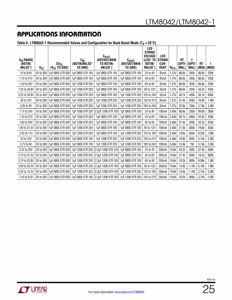
APPLICATIONS INFORMATIONTable 6. LTM8042-1 Recommended Values and Configuration for Buck-Boost Mode (TA = 25°C)
VIN RANGE (BSTIN/BKLED–) VCC
CVCC (VCC TO GND)
CIN (BSTIN/BKLED–
TO GND)
COUT1 (BSTOUT/BKIN
TO BSTIN/BKLED–)
COUT2 (BSTOUT/BKIN
TO GND)
LED STRING VOLTAGE (LED+ TO BSTIN/
BKLED–)
LED STRING
CUR-RENT RCTL
RT (OPTI-MAL)
f (OPTI-MAL)
RT (MIN)
f (MAX)
1V to 9.5V 3V to 30V 1µF 0805 X7R 50V 1µF 0805 X7R 10V 1µF 0805 X7R 10V 1µF 0805 X7R 10V 2V to 4V 35mA 1.27k 86.6k 250k 86.6k 250k
1.1V to 21V 3V to 30V 1µF 0805 X7R 50V 1µF 0805 X7R 16V 1µF 0805 X7R 10V 1µF 0805 X7R 10V 4V to 6V 35mA 1.27k 86.6k 250k 86.6k 250k
1.3V to 24V 3V to 30V 1µF 0805 X7R 50V 1µF 1206 X7R 25V 1µF 0805 X7R 10V 1µF 0805 X7R 10V 6V to 9V 35mA 1.27k 86.6k 250k 86.6k 250k
1.5V to 20.8V 3V to 30V 1µF 0805 X7R 50V 1µF 1206 X7R 25V 1µF 0805 X7R 16V 1µF 0805 X7R 16V 8V to 12V 35mA 1.27k 86.6k 250k 43.2k 450k
2.2V to 16.9V 3V to 30V 1µF 0805 X7R 50V 1µF 1206 X7R 25V 1µF 0805 X7R 16V 1µF 1206 X7R 25V 12V to 16V 35mA 1.27k 48.7k 400k 30.1k 600k
3V to 12V 3V to 30V 1µF 0805 X7R 50V 1µF 1206 X7R 25V 1µF 1206 X7R 25V 1µF 1206 X7R 25V 15V to 21V 35mA 1.27k 37.4k 500k 10.0k 1.4M
3.8V to 9V 3V to 30V 1µF 0805 X7R 50V 1µF 1206 X7R 25V 1µF 1206 X7R 25V 1µF 1206 X7R 25V 18V to 24V 35mA 1.27k 22.6k 750k 3.74k 2.5M
1.1V to 24V 3V to 30V 1µF 0805 X7R 50V 1µF 1206 X7R 25V 2.2µF 1206 X7R 10V 1µF 0805 X7R 10V 2V to 4V 100mA 3.40k 86.6k 250k 69.8k 300k
1.3V to 27V 3V to 30V 1µF 0805 X7R 50V 1µF 1206 X7R 25V 1µF 0805 X7R 10V 1µF 0805 X7R 10V 4V to 6V 100mA 3.40k 48.7k 400k 43.2k 450k
1.6V to 24V 3V to 30V 1µF 0805 X7R 50V 1µF 1206 X7R 25V 1µF 0805 X7R 10V 1µF 0805 X7R 10V 6V to 9V 100mA 3.40k 37.4k 500k 33.2k 550k
1.9V to 21.5V 3V to 30V 1µF 0805 X7R 50V 1µF 1206 X7R 25V 1µF 0805 X7R 16V 1µF 0805 X7R 16V 8V to 12V 100mA 3.40k 21.0k 800k 19.6k 850k
2.5V to 17V 3V to 30V 1µF 0805 X7R 50V 1µF 1206 X7R 25V 1µF 0805 X7R 16V 1µF 1206 X7R 25V 12V to 16V 100mA 3.40k 19.6k 850k 8.25k 1.6M
3V to 12V 3V to 30V 1µF 0805 X7R 50V 1µF 0805 X7R 16V 1µF 1206 X7R 25V 1µF 1206 X7R 25V 15V to 21V 100mA 3.40k 19.6k 850k 3.74k 2.5M
3.7V to 9V 3V to 30V 1µF 0805 X7R 50V 1µF 0805 X7R 10V 1µF 1206 X7R 25V 1µF 1206 X7R 25V 18V to 24V 100mA 3.40k 15.8k 1M 3.74k 2.5M
2.2V to 29V 3V to 30V 1µF 0805 X7R 50V 1µF 1206 X7R 50V 2.2µF 1206 X7R 10V 1µF 0805 X7R 10V 2V to 4V 350mA 19.6k 43.2k 450k 37.4k 500k
2.7V to 27.5V 3V to 30V 1µF 0805 X7R 50V 1µF 1206 X7R 50V 2.2µF 1206 X7R 10V 1µF 0805 X7R 10V 4V to 6V 350mA 19.6k 27.4k 650k 18.2k 900k
3.7V to 23.8V 3V to 30V 1µF 0805 X7R 50V 1µF 1206 X7R 25V 2.2µF 1206 X7R 10V 1µF 0805 X7R 10V 6V to 9V 350mA 19.6k 18.2k 900k 9.09k 1.5M
3.8V to 20.2V 3V to 30V 1µF 0805 X7R 50V 1µF 1206 X7R 25V 2.2µF 1206 X7R 16V 1µF 0805 X7R 16V 8V to 12V 350mA 19.6k 14.0k 1.1M 6.19k 1.9M
5.3V to 15.2V 3V to 30V 1µF 0805 X7R 50V 1µF 1206 X7R 25V 2.2µF 1206 X7R 16V 1µF 1206 X7R 25V 12V to 16V 350mA 19.6k 14.0k 1.1M 3.74k 2.5M
7.4V to 9.3V 3V to 30V 1µF 0805 X7R 50V 1µF 0805 X7R 16V 2.2µF 1206 X7R 16V 1µF 1206 X7R 25V 15V to 21V 350mA 19.6k 18.2k 900k 3.74k 2.5M
LTM8042/LTM8042-1
2680421fb
For more information www.linear.com/LTM8042
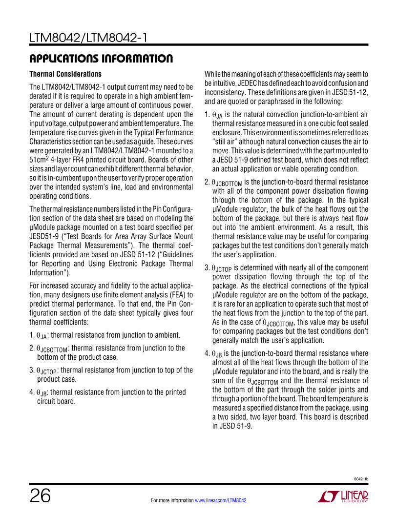
APPLICATIONS INFORMATIONThermal Considerations
The LTM8042/LTM8042-1 output current may need to be derated if it is required to operate in a high ambient tem-perature or deliver a large amount of continuous power. The amount of current derating is dependent upon the input voltage, output power and ambient temperature. The temperature rise curves given in the Typical Performance Characteristics section can be used as a guide. These curves were generated by an LTM8042/LTM8042-1 mounted to a 51cm2 4-layer FR4 printed circuit board. Boards of other sizes and layer count can exhibit different thermal behavior, so it is in-cumbent upon the user to verify proper operation over the intended system’s line, load and environmental operating conditions.
The thermal resistance numbers listed in the Pin Configura-tion section of the data sheet are based on modeling the µModule package mounted on a test board specified per JESD51-9 (“Test Boards for Area Array Surface Mount Package Thermal Measurements”). The thermal coef-ficients provided are based on JESD 51-12 (“Guidelines for Reporting and Using Electronic Package Thermal Information”).
For increased accuracy and fidelity to the actual applica-tion, many designers use finite element analysis (FEA) to predict thermal performance. To that end, the Pin Con-figuration section of the data sheet typically gives four thermal coefficients:
1. θJA: thermal resistance from junction to ambient.
2. θJCBOTTOM: thermal resistance from junction to the bottom of the product case.
3. θJCTOP: thermal resistance from junction to top of the product case.
4. θJB: thermal resistance from junction to the printed circuit board.
While the meaning of each of these coefficients may seem to be intuitive, JEDEC has defined each to avoid confusion and inconsistency. These definitions are given in JESD 51-12, and are quoted or paraphrased in the following:
1. θJA is the natural convection junction-to-ambient air thermal resistance measured in a one cubic foot sealed enclosure. This environment is sometimes referred to as “still air” although natural convection causes the air to move. This value is determined with the part mounted to a JESD 51-9 defined test board, which does not reflect an actual application or viable operating condition.
2. θJCBOTTOM is the junction-to-board thermal resistance with all of the component power dissipation flowing through the bottom of the package. In the typical µModule regulator, the bulk of the heat flows out the bottom of the package, but there is always heat flow out into the ambient environment. As a result, this thermal resistance value may be useful for comparing packages but the test conditions don’t generally match the user’s application.
3. θJCTOP is determined with nearly all of the component power dissipation flowing through the top of the package. As the electrical connections of the typical µModule regulator are on the bottom of the package, it is rare for an application to operate such that most of the heat flows from the junction to the top of the part. As in the case of θJCBOTTOM, this value may be useful for comparing packages but the test conditions don’t generally match the user’s application.
4. θJB is the junction-to-board thermal resistance where almost all of the heat flows through the bottom of the µModule regulator and into the board, and is really the sum of the θJCBOTTOM and the thermal resistance of the bottom of the part through the solder joints and through a portion of the board. The board temperature is measured a specified distance from the package, using a two sided, two layer board. This board is described in JESD 51-9.
LTM8042/LTM8042-1
2780421fb
For more information www.linear.com/LTM8042
APPLICATIONS INFORMATIONThe most appropriate way to use the coefficients is when running a detailed thermal analysis, such as FEA, which considers all of the thermal resistances simultaneously. None of them can be individually used to accurately pre-dict the thermal performance of the product, so it would be inappropriate to attempt to use any one coefficient to correlate to the junction temperature versus load graphs given in the LTM8042/LTM8042-1 data sheet.
A graphical representation of these thermal resistances is given in Figure 5.
The blue resistances are contained within the µModule regulator, and the green are outside.
80421 F05
µMODULE DEVICE
JUNCTION-TO-CASE (TOP)RESISTANCE
JUNCTION-TO-BOARD RESISTANCE
JUNCTION-TO-AMBIENT RESISTANCE (JESD 51-9 DEFINED BOARD)
CASE (TOP)-TO-AMBIENTRESISTANCE
BOARD-TO-AMBIENTRESISTANCE
JUNCTION-TO-CASE(BOTTOM) RESISTANCE
JUNCTION At
CASE (BOTTOM)-TO-BOARDRESISTANCE
The die temperature of the LTM8042/LTM8042-1 must be lower than the maximum rating of 125°C, so care should be taken in the layout of the circuit to ensure good heat sinking of the LTM8042/LTM8042-1. The bulk of the heat flow out of the LTM8042/LTM8042-1 is through the bottom of the module and the LGA pads into the printed circuit board. Consequently, a poor printed circuit board design can cause excessive heating, resulting in impaired performance or reliability. Please refer to the PCB Layout section for printed circuit board design suggestions.
Figure 5
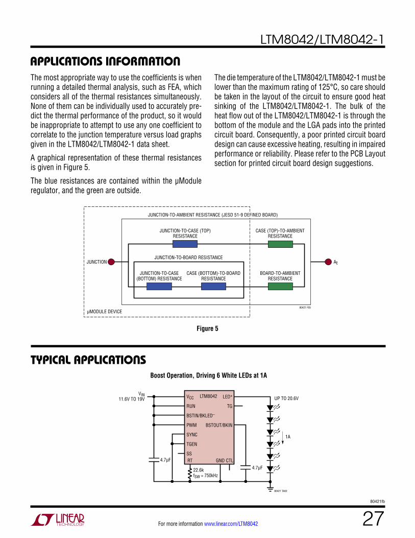
TYPICAL APPLICATIONSBoost Operation, Driving 6 White LEDs at 1A
80421 TA02
LTM8042
RT GND CTL
VCC
RUN
BSTIN/BKLED–
PWM
SYNC
TGEN
SS
VIN11.6V TO 19V LED+
TG
BSTOUT/BKIN
4.7µF
22.6kfSW = 750kHz
4.7µF
UP TO 20.6V
1A

LTM8042/LTM8042-1
2880421fb
For more information www.linear.com/LTM8042
Buck-Boost Mode, Driving 5 White LEDs at 500mA with PWM Dimming
Buck Mode, Driving 4 White LEDs at 1A
Boost Operation, Driving 9 White LEDs at 100mA
TYPICAL APPLICATIONS
80421 TA03
LTM8042 Si2319DS
UP TO 16.3V
RT GND CTL 2.2µF
7.32k19.6kfSW = 850kHz
1µF
VCC
RUN
PWM
TGEN
SYNC
SS
VIN7V TO 17.5V LED+
TG
BSTOUT/BKIN
BSTIN/BKLED–
1µF
500mA
80421 TA04
LTM8042
RT GND CTL4.7µF
15.8kfSW = 1MHz
2.2µF
UP TO 13.9VVCC
RUN
PWM
SYNC
TGEN
SS
VIN19V TO 30V LED+
TG
BSTOUT/BKIN
BSTIN/BKLED–
1µF
1A
80421 TA05
LTM8042-1
RT GND
Si2319DS
CTL
VCC
RUN
BSTIN/BKLED–
PWM
TGEN
SYNC
SS
VIN6V TO 22V LED+
TG
BSTOUT/BKIN
3.4k
2.2µF
2.2µF24.9kfSW = 700kHz
100mA
UP TO 29V
LTM8042/LTM8042-1
2980421fb
For more information www.linear.com/LTM8042
PACKAGE DESCRIPTION
PIN NAME PIN NAME PIN NAME PIN NAME PIN NAME PIN NAME
A1 GND B1 GND C1 GND D1 GND E1 GND F1 RUN
A2 GND B2 GND C2 GND D2 GND E2 GND F2 GND
A3 GND B3 GND C3 GND D3 GND E3 GND F3 GND
A4 GND B4 GND C4 GND D4 GND E4 GND F4 GND
A5 GND B5 GND C5 BSTIN/BKLED– D5 BSTIN/BKLED– E5 GND F5 GND
A6 VCC B6 VCC C6 BSTIN/BKLED– D6 BSTIN/BKLED– E6 GND F6 GND
A7 VCC B7 VCC C7 BSTIN/BKLED– D7 BSTIN/BKLED– E7 GND F7 GND
PIN NAME PIN NAME PIN NAME PIN NAME PIN NAME
G1 SYNC H1 RT J1 SS K1 PWM L1 GND
G2 GND H2 GND J2 GND K2 GND L2 CTL
G3 GND H3 GND J3 GND K3 GND L3 TGEN
G4 GND H4 GND J4 GND K4 GND L4 GND
G5 BSTOUT/BKIN H5 BSTOUT/BKIN J5 BSTOUT/BKIN K5 LED+ L5 LED+
G6 BSTOUT/BKIN H6 BSTOUT/BKIN J6 BSTOUT/BKIN K6 LED+ L6 LED+
G7 BSTOUT/BKIN H7 BSTOUT/BKIN J7 TG K7 LED+ L7 LED+
Pin Assignment Table (Arranged by Pin Number)
PACKAGE PHOTOGRAPH
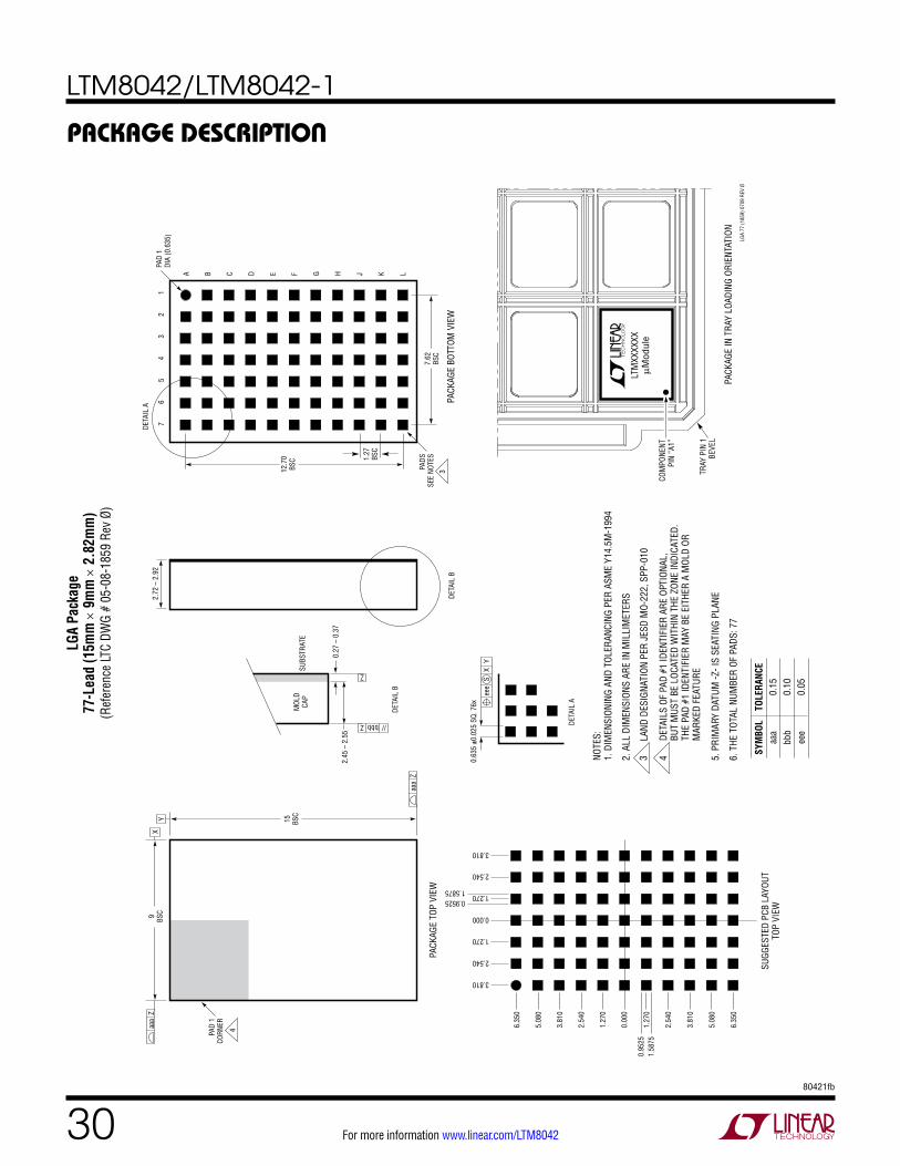
LTM8042/LTM8042-1
3080421fb
For more information www.linear.com/LTM8042
PACKAGE DESCRIPTION
LGA
Pack
age
77-L
ead
(15m
m ×
9m
m ×
2.8
2mm
)(R
efer
ence
LTC
DWG
# 05
-08-
1859
Rev
Ø)
NOTE
S:1.
DIM
ENSI
ONIN
G AN
D TO
LERA
NCIN
G PE
R AS
ME
Y14.
5M-1
994
2. A
LL D
IMEN
SION
S AR
E IN
MIL
LIM
ETER
S
LAN
D DE
SIGN
ATIO
N PE
R JE
SD M
O-22
2, S
PP-0
10
5. P
RIM
ARY
DATU
M -Z
- IS
SEAT
ING
PLAN
E
6. T
HE T
OTAL
NUM
BER
OF P
ADS:
77
43
DETA
ILS
OF P
AD #
1 ID
ENTI
FIER
ARE
OPT
IONA
L,BU
T M
UST
BE L
OCAT
ED W
ITHI
N TH
E ZO
NE IN
DICA
TED.
THE
PAD
#1 ID
ENTI
FIER
MAY
BE
EITH
ER A
MOL
D OR
M
ARKE
D FE
ATUR
E
SYM
BOL
aaa
bbb
eee
TOLE
RANC
E0.
150.
100.
05
2.72
– 2
.92
DETA
IL B
DETA
IL B
SUBS
TRAT
EM
OLD
CAP
0.27
– 0
.37
2.45
– 2
.55
// bbb Z
Z
15 BSC
PACK
AGE
TOP
VIEW
9 BSC
4PAD
1CO
RNER
XY
aaa
Z
aaa
Z
DETA
IL A
12.7
0BS
C 1.27
BSC
7.62
BSC
LKJHGFEDCB
PACK
AGE
BOTT
OM V
IEW
3PADS
SEE
NOTE
S
A
12
34
56
7
DETA
IL A
0.63
5 ±0
.025
SQ.
76x
SY
Xee
e
SUGG
ESTE
D PC
B LA
YOUT
TOP
VIEW
0.00
0
1.27
0
1.27
0
2.54
0
2.54
0
3.81
0
3.81
0
5.08
0
5.08
0
6.35
0
6.35
0
3.810
1.270
2.540
0.000
1.270
3.810
2.540
LGA
77 (1
859)
070
9 RE
V Ø
PAD
1DI
A (0
.635
)
0.95
251.
5875
0.95251.5875
PACK
AGE
IN T
RAY
LOAD
ING
ORIE
NTAT
ION
LTM
XXXX
XXµ
Mod
ule
TRAY
PIN
1BE
VEL
COM
PONE
NTPI
N “A
1”
LGA
Pack
age
77-L
ead
(15m
m ×
9m
m ×
2.8
2mm
)(R
efer
ence
LTC
DW
G #
05-0
8-18
59 R
ev Ø
)
LTM8042/LTM8042-1
3180421fb
For more information www.linear.com/LTM8042
Information furnished by Linear Technology Corporation is believed to be accurate and reliable. However, no responsibility is assumed for its use. Linear Technology Corporation makes no representa-tion that the interconnection of its circuits as described herein will not infringe on existing patent rights.
REVISION HISTORYREV DATE DESCRIPTION PAGE NUMBER
A 01/11 Updated features.Updated ILED conditions in the Electrical Characteristics section.Updated text in the Operation section.Updated text in the Setting the Switching Frequency section.
13
1516
B 11/14 Corrected Top Mark for LTM8042-1 2
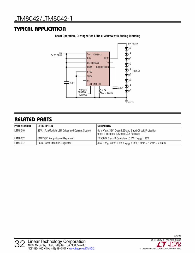
LTM8042/LTM8042-1
3280421fb
For more information www.linear.com/LTM8042 LINEAR TECHNOLOGY CORPORATION 2010
LT 1114 REV B • PRINTED IN USALinear Technology Corporation1630 McCarthy Blvd., Milpitas, CA 95035-7417(408) 432-1900 FAX: (408) 434-0507 www.linear.com/LTM8042
RELATED PARTS
TYPICAL APPLICATION
PART NUMBER DESCRIPTION COMMENTS
LTM8040 36V, 1A, µModule LED Driver and Current Source 4V ≤ VIN ≤ 36V; Open LED and Short-Circuit Protection, 9mm × 15mm × 4.32mm LGA Package
LTM8032 EMC 36V, 2A, µModule Regulator EN55022 Class B Compliant; 0.8V ≤ VOUT ≤ 10V
LTM4607 Buck-Boost µModule Regulator 4.5V ≤ VIN ≤ 36V; 0.8V ≤ VOUT ≤ 25V, 15mm × 15mm × 2.8mm
Boost Operation, Driving 9 Red LEDs at 350mA with Analog Dimming
80421 TA06
LTM8042
RTGNDCTL
VCC
RUN
BSTIN/BKLED–
PWM
SYNC
TGEN
SS
VIN7V TO 24.8V
LED+
TG
BSTOUT/BKIN
2.2µF
ANALOGCONTROLVOLTAGE
19.6kfSW = 850kHz
2.2µF
350mA
UP TO 28V


![INDEX []cranes over 100 tons index lg-1550 liebherr ltm 1500 liebherr ltm-1400 liebherr ltm-1225 liebherr ltm-1220 liebherr ltm-1130 liebherr ltr-1100 liebherr](https://img.pdfslide.net/doc/110x75/5e6bde846cd1285bdf61f15a/index-cranes-over-100-tons-index-lg-1550-liebherr-ltm-1500-liebherr-ltm-1400.jpg)


![INDEX [] LG-1550 LIEBHERR LTM 1500 LIEBHERR LTM-1400 LIEBHERR LTM-1225 LIEBHERR LTM-1220 LIEBHERR ... Cranes_over100tons.pdf](https://img.pdfslide.net/doc/110x75/5b07232e7f8b9ae9628e08fa/index-lg-1550-liebherr-ltm-1500-liebherr-ltm-1400-liebherr-ltm-1225-liebherr.jpg)