Embed Size (px)
Citation preview
LITE-ON DCC
RELEASE
LITE-ON Technology Corp. / OptoelectronicsNo.90,Chien 1 Road, Chung Ho, New Taipei City 23585, Taiwan, R.O.C.
Tel: 886-2-2222-6181 Fax: 886-2-2221-1948 / 886-2-2221-0660http://www.liteon.com/opto
SMD LEDProduct Data SheetLTSA-G6SPVSKT Spec No.: DS35-2016-0078Effective Date: 10/01/2016
Revision: -
BNS-OD-FC001/A4
BNS-OD-FC001/A4
BNS-OD-FC001/A4
BNS-OD-FC001/A4

1/12 Part No. : LTSA-G6SPVSKT BNS-OD-FC002/A4
SMD LED LTSA-G6SPVSKT
t
1. Description
SMD LEDs from Lite-On are available in miniature sizes and special configurations for automated PC board assembly and
space-sensitive applications. These SMD LEDs are suitable for use in a wide variety of Automotive.
1.1 Features
Meet ROHS
Package in 8mm tape on 7" diameter reels
Preconditioning: accelerate to JEDEC level 3
EIA STD package
I.C. compatible
Compatible with automatic placement equipment
Compatible with infrared reflow solder process
1.2 Applications
Aftermarket: accessory applications,
2. Package Dimensions
Part No. Lens Color Source Color
LTSA-G6SPVSKT Water clear AlInGaP Yellow
Notes:
1. All dimensions are in millimeters.
2. Tolerance is ±0.2 mm (.008") unless otherwise noted.
3. ANODE lead frame is heat sink of LED.

2/12 Part No. : LTSA-G6SPVSKT BNS-OD-FC002/A4
SMD LED LTSA-G6SPVSKT
t
3.2 Thermal Characteristics
Parameter Symbol TYP. MAX. Unit
Thermal Resistance (Junction – Ambient)Note Rth JA 50 - °C /W
Thermal Resistance (Junction – Solder Point)Note
Rth JS 30 - °C /W
Junction Temperature TJ - 115 °C
Note: Rth JA Measurement Condition
Substrate: FR4 (t=1.6mm) / Pattern Size: 16mm2
3. Rating and Characteristics
3.1 Absolute Maximum Ratings at Ta=25°C
Parameter LTSA-G6SPVSKT Unit
Power Dissipation 530 mW
Peak Forward Current
(1/10 Duty Cycle, 0.1ms Pulse Width)
1000 mA
DC Forward Current 200 mA
Operating Temperature Range -40°C to +110°C
Storage Temperature Range -40°C to + 110°C
Infrared Soldering Condition 260 °C For 10 Seconds

3/12 Part No. : LTSA-G6SPVSKT BNS-OD-FC002/A4
SMD LED LTSA-G6SPVSKT
t 3.3 Suggest IR Reflow Condition for Pb Free Process:
IR-Reflow Soldering Profile for lead free soldering (Acc. to J-STD-020)

4/12 Part No. : LTSA-G6SPVSKT BNS-OD-FC002/A4
SMD LED LTSA-G6SPVSKT
t
Notes:
1. Luminous intensity is measured with a light sensor and filter combination that approximates the CIE
eye-response curve
2. 1/2 is the off-axis angle at which the luminous intensity is half the axial luminous intensity.
3. The dominant wavelength, λd is derived from the CIE chromaticity diagram and represents the single
wavelength which defines the color of the device. Dominate Wavelength Tolerance is +/- 1nm.
4. Forward Voltage Tolerance is +/- 0.1 volt.
5. Reverse voltage (VR) condition is applied to IR test only. The device is not designed for reverse operation.
3.4 Electrical / Optical Characteristics at Ta=25°C
Parameter Symbol Part No.
LTSA- Min. Typ. Max. Unit
Test
Condition
Luminous Intensity IV G6SPVSKT 3.55 - 9.0 cd IF = 140mA
Note 1
Viewing Angle 21/2 G6SPVSKT - 120 - deg Note 2 (Fig.5)
Peak Emission Wavelength P G6SPVSKT - 592 - nm Measurement
@Peak (Fig.1)
Dominant Wavelength d G6SPVSKT 583 - 595 nm IF = 140mA
Note 3
Spectral Line Half-Width G6SPVSKT - 18 - nm
Forward Voltage VF G6SPVSKT 1.9 - 2.65 V IF = 140mA
Note 4
Reverse Current IR G6SPVSKT - 10 μA VR =5V
Note 5
5/12 Part No. : LTSA-G6SPVSKT BNS-OD-FC002/A4
SMD LED LTSA-G6SPVSKT
t
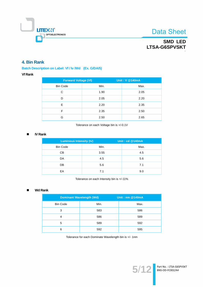
4. Bin Rank
Batch Description on Label: Vf / Iv /Wd (Ex. G/DA/5)
Vf Rank
Forward Voltage (Vf) Unit : V @140mA
Bin Code Min. Max.
C 1.90 2.05
D 2.05 2.20
E 2.20 2.35
F 2.35 2.50
G 2.50 2.65
Tolerance on each Voltage bin is +/-0.1V
IV Rank
Luminous Intensity (Iv) Unit : cd @140mA
Bin Code Min. Max.
CB 3.55 4.5
DA 4.5 5.6
DB 5.6 7.1
EA 7.1 9.0
Tolerance on each Intensity bin is +/-11%
Wd Rank
Dominant Wavelength (Wd) Unit : nm @140mA
Bin Code Min. Max.
3 583 586
4 586 589
5 589 592
6 592 595
Tolerance for each Dominate Wavelength bin is +/- 1nm

6/12 Part No. : LTSA-G6SPVSKT BNS-OD-FC002/A4
SMD LED LTSA-G6SPVSKT
t
5. Typical Electrical / Optical Characteristics Curves.
25°C Ambient Temperature Unless Special Noted)
Fig. 2 SPATIAL DISTRIBUTION

7/12 Part No. : LTSA-G6SPVSKT BNS-OD-FC002/A4
SMD LED LTSA-G6SPVSKT
t 6. User Guide
6.1 Cleaning
Do not use unspecified chemical liquid to clean LED they could harm the package. If cleaning is necessary, immerse the
LED in ethyl alcohol or isopropyl alcohol at normal temperature for less than one minute.
6.2 Recommend Printed Circuit Board Attachment Pad
Infrared
Reflow Soldering
6.3 Package Dimensions of Tape And Reel
Note:
1. All dimensions are in millimeters.

8/12 Part No. : LTSA-G6SPVSKT BNS-OD-FC002/A4
SMD LED LTSA-G6SPVSKT
t 6.4 Package Dimensions of Reel
Notes:
1. Empty component pockets sealed with top cover tape.
2. 7 inch reel 1000 pieces per reel.
3. The maximum number of consecutive missing lamps is two.
4. In accordance with ANSI/EIA 481 specifications.

9/12 Part No. : LTSA-G6SPVSKT BNS-OD-FC002/A4
SMD LED LTSA-G6SPVSKT
t 7. Cautions
7.1 Application
The LEDs described here are intended to be used for ordinary electronic equipment (such as office equipment,
communication equipment and household applications).Consult Liteon’s Sales in advance for information on applications
in which exceptional reliability is required, particularly when the failure or malfunction of the LEDs may directly jeopardize
life or health (such as in aviation, transportation, traffic control equipment, medical and life support systems and safety
devices).
7.2 Storage
The package is sealed:
The LEDs should be stored at 30°C or less and 70%RH or less. And the LEDs are limited to use within one year, while
the LEDs is packed in moisture-proof package with the desiccants inside.
The package is opened:
The storage ambient for the LEDs should not exceed 30°C temperature and 60% relative humidity.
It is recommended that LEDs out of their original packaging are IR-reflowed within 168hrs.
For extended storage out of their original packaging, it is recommended that the LEDs be stored in a sealed container
with appropriate desiccant, or in a desiccators with nitrogen ambient.
LEDs stored out of their original packaging for more than 168hrs should be baked at about 60 °C for at least 48 hours
before solder assembly.
7.3 Cleaning
Use alcohol-based cleaning solvents such as isopropyl alcohol to clean the LED if necessary.
7.4 Soldering
Recommended soldering conditions:
Reflow soldering Soldering iron
Pre-heat
Pre-heat time
Peak temperature
Soldering time
150~200°C
120 sec. Max.
260°C Max.
10 sec. Max.(Max. two times)
Temperature
Soldering time
300°C Max.
3 sec. Max.
(one time only)
Notes:
Because different board designs use different number and types of devices, solder pastes, reflow ovens, and circuit
boards, no single temperature profile works for all possible combinations.
However, you can successfully mount your packages to the PCB by following the proper guidelines and PCB-specific
characterization.
LITE-ON Runs both component-level verification using in-house KYRAMX98 reflow chambers and board-level assembly.
The results of this testing are verified through post-reflow reliability testing.Profiles used at LITE-ON are based on
JEDEC standards to ensure that all packages can be successfully and reliably surface mounted.
Figure on page3 shows a sample temperature profile compliant to JEDEC standards. You can use this example as a
generic target to set up your reflow process. You should adhere to the JEDEC profile limits as well as specifications and
recommendations from the solder paste manufacturer to avoid damaging the device and create a reliable solder joint.

10/12 Part No. : LTSA-G6SPVSKT BNS-OD-FC002/A4
SMD LED LTSA-G6SPVSKT
t 7.5 Drive Method
A LED is a current-operated device. In order to ensure intensity uniformity on multiple LEDs connected in parallel in an
application, it is recommended that a current limiting resistor be incorporated in the drive circuit, in series with each LED
as shown in Circuit A below.
Circuit model A Circuit model B
(A) Recommended circuit.
(B) The brightness of each LED might appear different due to the differences in the I-V characteristics
of those LEDs.
7.6 ESD (Electrostatic Discharge)
Static Electricity or power surge will damage the LED.
Suggestions to prevent ESD damage:
Use of a conductive wrist band or anti-electrostatic glove when handling these LEDs.
All devices, equipment, and machinery must be properly grounded.
Work tables, storage racks, etc. should be properly grounded.
Use ion blower to neutralize the static charge which might have built up on surface of the LED’s plastic lens as a
result of friction between LEDs during storage and handling.
ESD-damaged LEDs will exhibit abnormal characteristics such as high reverse leakage current, low forward voltage, or
“ no lightup ” at low currents.
To verify for ESD damage, check for “ lightup ” and Vf of the suspect LEDs at low currents.
The Vf of “ good ” LEDs should be >[email protected] for InGaN product and >[email protected] for AlInGaP product.
LED LED

11/12 Part No. : LTSA-G6SPVSKT BNS-OD-FC002/A4
SMD LED LTSA-G6SPVSKT
t 8. Reliability Test
8.1 Test Item/Condition:
No. Test item Test condition Reference standard
1 Pre-conditioning
MSL 3
125℃, 24 hrs baking
Moisture Soak 60℃/60% 52 hrs
Interval: 15mins ~ 4 hours to do IR-Reflow
JESD22 A-113
2 High Temperature Forward Bias (HTFB)
Ta=70 ± 2°C IF: 200 mA 1000 hrs
EIAJ ED-4701/100 (101)
3 High Temperature Forward Bias (HTFB)
Ta=110 ± 2°C IF: 50mA 1000 hrs
EIAJ ED-4701/100 (101)
4 Low Temperature Operating Life
Ta=-40 ± 2°C IF=200mA 1000 hrs
EIAJ ED-4701/100 (101)
5 High Temperature
Storage Ta=110 ± 2°C 1000 hrs
EIAJ ED-4701/100 (201)
6 Low Temperature Storage
Ta=-40 ± 2°C 1000 hrs
EIAJ ED-4701/100 (202)
7 High Temperature High Humidity Bias (HTHHB)
Ta=60℃, Rh=90%
IF=200mA
1000 hrs
EIAJ ED-4701/100 (102)
8 Thermal Shock (air to air)
-40℃ ± 5℃ ~ 100 ± 5℃
30min 30min
300cycles
EIAJ ED-4701/300 (307)
9 Temperature Cycle (TC)
-40°C~ 25°C ~100°C~ 25°C 30 min 5 min 30 min 5 min
300 cycles
EIAJ ED-4701/100 (105)
10 Resistance to Solder
Heat Tsld=260°C, 10sec. 3times JESD22A-111
11 Solderability Tsld = 245± 5°C, 5sec,
Leas-free Solder
J-STD-002
JESD22B102

12/12 Part No. : LTSA-G6SPVSKT BNS-OD-FC002/A4
SMD LED LTSA-G6SPVSKT
t
9. Others
The appearance and specifications of the product may be modified for improvement without prior notice.
10. Suggested Checking List
Training and Certification
1. Everyone working in a static-safe area is ESD-certified?
2. Training records kept and re-certification dates monitored?
Static-Safe Workstation & Work Areas
1. Static-safe workstation or work-areas have ESD signs?
2. All surfaces and objects at all static-safe workstation and within 1 ft measure less than 100V?
3. All ionizer activated, positioned towards the units?
4. Each work surface mats grounding is good?
Personnel Grounding
1. Every person (including visitors) handling ESD sensitive (ESDS) items wears wrist strap, heel strap or conductive shoes with
conductive flooring?
2. If conductive footwear used, conductive flooring also present where operator stand or walk?
3. Garments, hairs or anything closer than 1 ft to ESD items measure less than 100V*?
4. Every wrist strap or heel strap/conductive shoes checked daily and result recorded for all DLs?
5. All wrist strap or heel strap checkers calibration up to date?
Note: *50V for InGaN LED.
Device Handling
1. Every ESDS items identified by EIA-471 labels on item or packaging?
2. All ESDS items completely inside properly closed static-shielding containers when not at static-safe workstation?
3. No static charge generators (e.g. plastics) inside shielding containers with ESDS items?
4. All flexible conductive and dissipative package materials inspected before reuse or recycles?
Others
1. Audit result reported to entity ESD control coordinator?
2. Corrective action from previous audits completed?
3. Are audit records complete and on file?