Embed Size (px)
Citation preview

Application ReportSLLA054A - February 2002
1
LVDS Multidrop ConnectionsElliott Cole, P.E. Mixed Signal Products
ABSTRACT
This application report describes design considerations for low-voltage differential swing (LVDS)multidrop connections. The report describes the maximum number of receivers possible versussignaling rate, signal quality, line length, output jitter, and common-mode voltage range when multidroptesting on a single LVDS line driver transmitting to numerous daisy-chained LVDS receivers.
The LVDS receivers are wired to simulate a wire-wrapped or printed circuit backplane environment.The receivers are tested to monitor system response for different signaling rates and a varied numberof receivers.
Contents
1 Introduction 3. . . . . . . . . . . . . . . . . . . . . . . . . . . . . . . . . . . . . . . . . . . . . . . . . . . . . . . . . . . . . . . . . . . . . . . . .
2 Maximum Number of Receivers 3. . . . . . . . . . . . . . . . . . . . . . . . . . . . . . . . . . . . . . . . . . . . . . . . . . . . . . . 2.1 Best C ase Analysis 3. . . . . . . . . . . . . . . . . . . . . . . . . . . . . . . . . . . . . . . . . . . . . . . . . . . . . . . . . . . . . . .
2.1.1 DC Electrical Models 3. . . . . . . . . . . . . . . . . . . . . . . . . . . . . . . . . . . . . . . . . . . . . . . . . . . . . . . 2.1.2 Driver Analysis 4. . . . . . . . . . . . . . . . . . . . . . . . . . . . . . . . . . . . . . . . . . . . . . . . . . . . . . . . . . . . 2.1.3 Common-Mode Load 5. . . . . . . . . . . . . . . . . . . . . . . . . . . . . . . . . . . . . . . . . . . . . . . . . . . . . . . 2.1.4 Differential Load 5. . . . . . . . . . . . . . . . . . . . . . . . . . . . . . . . . . . . . . . . . . . . . . . . . . . . . . . . . . . 2.1.5 Receiver Input Leakage 5. . . . . . . . . . . . . . . . . . . . . . . . . . . . . . . . . . . . . . . . . . . . . . . . . . . . .
2.2 Worst Case Analysis 6. . . . . . . . . . . . . . . . . . . . . . . . . . . . . . . . . . . . . . . . . . . . . . . . . . . . . . . . . . . . . . 2.2.1 TIA/EIA-644 Requirements 6. . . . . . . . . . . . . . . . . . . . . . . . . . . . . . . . . . . . . . . . . . . . . . . . . . 2.2.2 TI LVDS Characteristics 7. . . . . . . . . . . . . . . . . . . . . . . . . . . . . . . . . . . . . . . . . . . . . . . . . . . . .
3 Maximum Signaling Rate Obstacles 7. . . . . . . . . . . . . . . . . . . . . . . . . . . . . . . . . . . . . . . . . . . . . . . . . . . 3.1 Driver Output Loading 8. . . . . . . . . . . . . . . . . . . . . . . . . . . . . . . . . . . . . . . . . . . . . . . . . . . . . . . . . . . . . 3.2 Intersymbol Interference 8. . . . . . . . . . . . . . . . . . . . . . . . . . . . . . . . . . . . . . . . . . . . . . . . . . . . . . . . . . . 3.3 Skew in Parallel Buses 9. . . . . . . . . . . . . . . . . . . . . . . . . . . . . . . . . . . . . . . . . . . . . . . . . . . . . . . . . . . . 3.4 Termination 9. . . . . . . . . . . . . . . . . . . . . . . . . . . . . . . . . . . . . . . . . . . . . . . . . . . . . . . . . . . . . . . . . . . . . . 3.5 Allowable Jitter 10. . . . . . . . . . . . . . . . . . . . . . . . . . . . . . . . . . . . . . . . . . . . . . . . . . . . . . . . . . . . . . . . . . 3.6 External Noise Coupling 11. . . . . . . . . . . . . . . . . . . . . . . . . . . . . . . . . . . . . . . . . . . . . . . . . . . . . . . . . . 3.7 Common-Mode Voltage Range 11. . . . . . . . . . . . . . . . . . . . . . . . . . . . . . . . . . . . . . . . . . . . . . . . . . . .
4 Bench Verification 11. . . . . . . . . . . . . . . . . . . . . . . . . . . . . . . . . . . . . . . . . . . . . . . . . . . . . . . . . . . . . . . . . . 4.1 The Multidrop Setup 11. . . . . . . . . . . . . . . . . . . . . . . . . . . . . . . . . . . . . . . . . . . . . . . . . . . . . . . . . . . . . 4.2 Equipment Setup 14. . . . . . . . . . . . . . . . . . . . . . . . . . . . . . . . . . . . . . . . . . . . . . . . . . . . . . . . . . . . . . . .
5 Measurement Results 16. . . . . . . . . . . . . . . . . . . . . . . . . . . . . . . . . . . . . . . . . . . . . . . . . . . . . . . . . . . . . . . 5.1 Output Jitter From Receiver 36 With Different Cable Lengths 16. . . . . . . . . . . . . . . . . . . . . . . . . . 5.2 Output Jitter From a Single Point-to-Point Receiver 17. . . . . . . . . . . . . . . . . . . . . . . . . . . . . . . . . . 5.3 Output Jitter of Varied Load Conditions 18. . . . . . . . . . . . . . . . . . . . . . . . . . . . . . . . . . . . . . . . . . . . . 5.4 Percent Output Jitter From Every Fourth Load 22. . . . . . . . . . . . . . . . . . . . . . . . . . . . . . . . . . . . . . .
6 Conclusion 23. . . . . . . . . . . . . . . . . . . . . . . . . . . . . . . . . . . . . . . . . . . . . . . . . . . . . . . . . . . . . . . . . . . . . . . . .

SLLA054A
2 LVDS Multidrop Connections
6.1 Receiver Number vs Cable Length 23. . . . . . . . . . . . . . . . . . . . . . . . . . . . . . . . . . . . . . . . . . . . . . . . . 6.2 Receiver Number vs Signaling Rate 26. . . . . . . . . . . . . . . . . . . . . . . . . . . . . . . . . . . . . . . . . . . . . . . . 6.3 Receiver Number vs Common-Mode Voltage Range 29. . . . . . . . . . . . . . . . . . . . . . . . . . . . . . . . .
7 References 30. . . . . . . . . . . . . . . . . . . . . . . . . . . . . . . . . . . . . . . . . . . . . . . . . . . . . . . . . . . . . . . . . . . . . . . . .
List of Figures
1 Common Mode and Differential LVDS Bus Model 3. . . . . . . . . . . . . . . . . . . . . . . . . . . . . . . . . . . . . . . . . . . 2 Differential Line Driver Model 4. . . . . . . . . . . . . . . . . . . . . . . . . . . . . . . . . . . . . . . . . . . . . . . . . . . . . . . . . . . . . 3 Simplified LVDS Driver Model 4. . . . . . . . . . . . . . . . . . . . . . . . . . . . . . . . . . . . . . . . . . . . . . . . . . . . . . . . . . . . . 4 Common Mode and Differential Driver Models 4. . . . . . . . . . . . . . . . . . . . . . . . . . . . . . . . . . . . . . . . . . . . . . 5 SN65LVDS31 Simplified Driver Model 5. . . . . . . . . . . . . . . . . . . . . . . . . . . . . . . . . . . . . . . . . . . . . . . . . . . . . 6 SN65LVDS31 Common Mode and Differential Driver Models 5. . . . . . . . . . . . . . . . . . . . . . . . . . . . . . . . . 7 Simplified SN65LVDS32 Receiver Model 6. . . . . . . . . . . . . . . . . . . . . . . . . . . . . . . . . . . . . . . . . . . . . . . . . . . 8 SN65LVDS32 Common Mode and Differential Driver Models 6. . . . . . . . . . . . . . . . . . . . . . . . . . . . . . . . . 9 Spec-Compliant 20 Receiver Model 7. . . . . . . . . . . . . . . . . . . . . . . . . . . . . . . . . . . . . . . . . . . . . . . . . . . . . . . 10 Loading Effects at a Receiver Input 8. . . . . . . . . . . . . . . . . . . . . . . . . . . . . . . . . . . . . . . . . . . . . . . . . . . . . . . 11 Data Error Pattern 9. . . . . . . . . . . . . . . . . . . . . . . . . . . . . . . . . . . . . . . . . . . . . . . . . . . . . . . . . . . . . . . . . . . . . . 12 Typical Eye Pattern 10. . . . . . . . . . . . . . . . . . . . . . . . . . . . . . . . . . . . . . . . . . . . . . . . . . . . . . . . . . . . . . . . . . . 13 Multidrop System With TI LVDS Evaluation Modules 12. . . . . . . . . . . . . . . . . . . . . . . . . . . . . . . . . . . . . . . 14 Berg Sticks Connected to One Receiver Channel on the EVM 13. . . . . . . . . . . . . . . . . . . . . . . . . . . . . . 15 Multidrop Bank of 36 Receivers 14. . . . . . . . . . . . . . . . . . . . . . . . . . . . . . . . . . . . . . . . . . . . . . . . . . . . . . . . . 16 Test Setup With Instrumentation 15. . . . . . . . . . . . . . . . . . . . . . . . . . . . . . . . . . . . . . . . . . . . . . . . . . . . . . . . 17 Output Jitter From Receiver 36 With Different Cable Lengths 16. . . . . . . . . . . . . . . . . . . . . . . . . . . . . . . 18 Output Jitter vs Signaling Rate at Different Cable Lengths 17. . . . . . . . . . . . . . . . . . . . . . . . . . . . . . . . . . 19 Output Jitter From a Single Point-to-Point Receiver 18. . . . . . . . . . . . . . . . . . . . . . . . . . . . . . . . . . . . . . . . 20 Output Jitter of a Nine Receiver Load Bank 19. . . . . . . . . . . . . . . . . . . . . . . . . . . . . . . . . . . . . . . . . . . . . . . 21 Output Jitter of an Eighteen Receiver Load Bank 19. . . . . . . . . . . . . . . . . . . . . . . . . . . . . . . . . . . . . . . . . . 22 Output Jitter of a Twenty-Seven Receiver Load Bank 20. . . . . . . . . . . . . . . . . . . . . . . . . . . . . . . . . . . . . . 23 Output Jitter With a 1 m Cable and a Varied Number of Receivers 20. . . . . . . . . . . . . . . . . . . . . . . . . . . 24 Output Jitter With a 3 m Cable and a Varied Number of Receivers 21. . . . . . . . . . . . . . . . . . . . . . . . . . . 25 Output Jitter With a 10 m Cable and a Varied Number of Receivers 21. . . . . . . . . . . . . . . . . . . . . . . . . . 26 Output Jitter With a 30 m Cable and a Varied Number of Receivers 22. . . . . . . . . . . . . . . . . . . . . . . . . . 27 Percent Output Jitter From Every Fourth Load 23. . . . . . . . . . . . . . . . . . . . . . . . . . . . . . . . . . . . . . . . . . . . 28 Percent Output Jitter From Each Multidrop Load 24. . . . . . . . . . . . . . . . . . . . . . . . . . . . . . . . . . . . . . . . . . 29 Percent Output Jitter From a 35 Drop 21 ns Load 25. . . . . . . . . . . . . . . . . . . . . . . . . . . . . . . . . . . . . . . . . 30 Output Jitter From an 18-Receiver 17.1 ns Load 25. . . . . . . . . . . . . . . . . . . . . . . . . . . . . . . . . . . . . . . . . . 31 Output Jitter From a 13-Receiver 12.3 ns Load 27. . . . . . . . . . . . . . . . . . . . . . . . . . . . . . . . . . . . . . . . . . . 32 Output Jitter From a 15-Receiver 14.3 ns Load 27. . . . . . . . . . . . . . . . . . . . . . . . . . . . . . . . . . . . . . . . . . . 33 Output Jitter From an 11-Receiver 10.4 ns Load 28. . . . . . . . . . . . . . . . . . . . . . . . . . . . . . . . . . . . . . . . . . 34 Load Propagation Delay vs Signaling Rate 29. . . . . . . . . . . . . . . . . . . . . . . . . . . . . . . . . . . . . . . . . . . . . . . 35 Receiver Number vs Common-Mode Voltage Range 30. . . . . . . . . . . . . . . . . . . . . . . . . . . . . . . . . . . . . .

SLLA054A
3 LVDS Multidrop Connections
1 Introduction
The most commonly used data transmission system, or topology, is known as the point-to-pointapplication. The term point-to-point is used to describe a unidirectional system that consists of asingle line driver connected to a single line receiver, that transmits data from point A to point Busing one speaker and one listener. The term multidrop, defines a topology where one drivertransmits data to more than one receiver. The multidrop application is the equivalent of sendingdata from point A to point B1, point B2, point B3, etc., since with this application, one speakermay have a whole room full of listeners.
In data transmission circuits, the output voltage transition time of a line driver is often the limitingfactor in determining a maximum signal rate. This is usually due to an output stage not beingfast enough to provide a decent pulse, however data rate limitations are also related to noisemargin, crosstalk, and radiated and conducted emissions. Many conventional line drivers have asingle-ended output with a long, slow voltage swing of several volts. A signaling rate may befurther constrained by the increase in power dissipation as the signaling rate increases.
2 Maximum Number of Receivers
Connecting multiple LVDS receivers to a single LVDS driver works well, but at some point,increasing the number of receivers overloads a single driver, and the system fails. The maximumnumber of receivers possible is examined in the following discussion with best case and worstcase modeling.
2.1 Best Case Analysis
2.1.1 DC Electrical Models
The effect that multiple receivers have on a driver is calculated by examining the output model ofan LVDS driver and the input model of an LVDS receiver. The common mode and differentialmodels shown in Figure 1 represent an LVDS bus consisting of an LVDS driver, theinterconnection, and the LVDS receiver.
Common Mode
ID RD
Differential
+IOCD(RP1D–RP2D)
ID RD
n(IL)
+ –
VGND
RL/nIT
RT
Terminationn loadsDriver
n(IL)
RL/n ITRT
+IOCT(RP1T–RP2T)
IOCD IOCT
VOCDVOCT
VODD
IODD
VODT
IODT
+IOCL(RP1L–RP2L)
IOCL
Figure 1. Common Mode and Differential LVDS Bus Model

SLLA054A
4 LVDS Multidrop Connections
2.1.2 Driver Analysis
Figure 2 displays an LVDS driver model from Annex C of the TIA/EIA-644 standard. The modelis complex, but useful in developing a simplified differential line driver model for the examinationof driver response to output load increases. For this purpose, the simple model of anSN65LVDS31 line driver is developed in Figure 3.
+V (3.0 V – 3.6 V)
CRA
+12 V A+
VOA
VOB
A+A–
CRC
VRB
+12 V A+
+V (3.0 V – 3.6 V)
RA
A– A–
RC
RC
A+A–
RB
VOA
VOB
RT 100
Figure 2. Differential Line Driver Model
I01 Z01
I02 Z02ZCMICM
Figure 3. Simplified LVDS Driver Model
Output differential drive and common-mode offset models are derived from the simplified modelof Figure 3 and modeled individually in Figure 4.
Z01 + Z02
ZCM + Z01 // Z02
1OC
Common Mode
+ –
IOC × (Z01 – Z02)
I02 + I02
Differential
ICM IO1 IO2 ZCM
ZCM ZO1 ZO2
Figure 4. Common Mode and Differential Driver Models

SLLA054A
5 LVDS Multidrop Connections
Values are assigned to each source and impedance by using data sheet specifications and IBISmodels for the SN65LVDS31. These values are obtained from a straight line approximation ofthe actual IBIS model and are shown in Figure 5.
4 mA550 Ω
980 µA550 Ω
4 mA
1225 Ω
Figure 5. SN65LVDS31 Simplified Driver Model
Using the derived values in this model, individual common mode and differentialmodels are developed in Figure 6.
1100 Ω
1OC
Common Mode
+ –
<25 mV
± 4 mA
Differential
1500 Ω800 µA
Figure 6. SN65LVDS31 Common Mode and Differential Driver Models
2.1.3 Common-Mode Load
The model for the common-mode output of the SN65LVDS31 shows the driver consists of asmall current source and a 1500-Ω load develops a 1.2-Vdc common-mode voltage. The currentsource is capable of maintaining the 1.2 Vdc within the limits of the 800-µA source, but loadsbeyond this limit causes the common-mode output to shift.
2.1.4 Differential Load
The nominal driver output is modeled differentially as a 4-mA source with an output impedanceof 1100-Ω load; the resulting (nominal) current is 3.66 mA at the termination resistor, producing adifferential voltage (Vod) of 366 mV across the inputs of the receiver. The LVDS standardspecifies a minimum differential voltage of 250 mV, which occurs if the termination resistancedecreases to 67 Ω. The differential model also contains an offset voltage modeled as a 25-mVvoltage source resulting from a mismatch of the individual outputs. This mismatch can cause theoutput voltage levels to change differentially by 50 mV as the current source varies. The opencircuit differential-output voltage of the driver without the 100-Ω termination resistor does notremain at 4.4 Vdc, but ramps up to Vcc.
2.1.5 Receiver Input Leakage
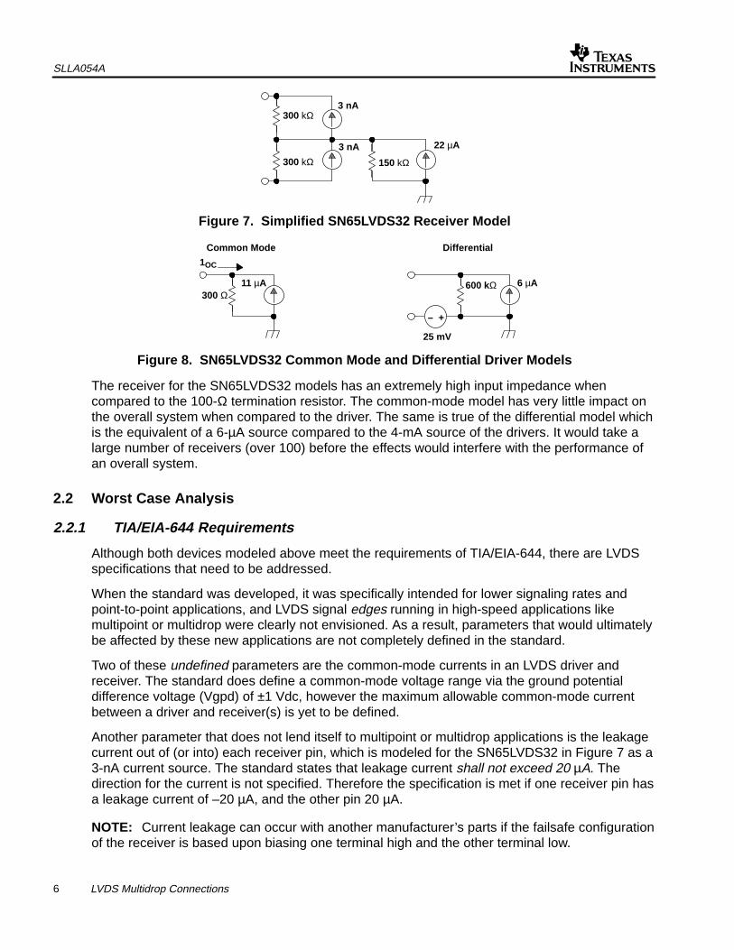
The SN65LVDS32 simplified receiver model in Figure 7 and the common-mode and differentialmodels of the receiver in Figure 8 are developed with the same derivation technique as theSN65LVDS31 driver.
SLLA054A
6 LVDS Multidrop Connections
3 nA300 kΩ
22 µA3 nA
150 kΩ300 kΩ
Figure 7. Simplified SN65LVDS32 Receiver Model
600 kΩ
1OC
Common Mode
+–
25 mV
Differential
300 Ω11 µA 6 µA
Figure 8. SN65LVDS32 Common Mode and Differential Driver Models
The receiver for the SN65LVDS32 models has an extremely high input impedance whencompared to the 100-Ω termination resistor. The common-mode model has very little impact onthe overall system when compared to the driver. The same is true of the differential model whichis the equivalent of a 6-µA source compared to the 4-mA source of the drivers. It would take alarge number of receivers (over 100) before the effects would interfere with the performance ofan overall system.
2.2 Worst Case Analysis
2.2.1 TIA/EIA-644 Requirements
Although both devices modeled above meet the requirements of TIA/EIA-644, there are LVDSspecifications that need to be addressed.
When the standard was developed, it was specifically intended for lower signaling rates andpoint-to-point applications, and LVDS signal edges running in high-speed applications likemultipoint or multidrop were clearly not envisioned. As a result, parameters that would ultimatelybe affected by these new applications are not completely defined in the standard.
Two of these undefined parameters are the common-mode currents in an LVDS driver andreceiver. The standard does define a common-mode voltage range via the ground potentialdifference voltage (Vgpd) of ±1 Vdc, however the maximum allowable common-mode currentbetween a driver and receiver(s) is yet to be defined.
Another parameter that does not lend itself to multipoint or multidrop applications is the leakagecurrent out of (or into) each receiver pin, which is modeled for the SN65LVDS32 in Figure 7 as a3-nA current source. The standard states that leakage current shall not exceed 20 µA. Thedirection for the current is not specified. Therefore the specification is met if one receiver pin hasa leakage current of –20 µA, and the other pin 20 µA.
NOTE: Current leakage can occur with another manufacturer’s parts if the failsafe configurationof the receiver is based upon biasing one terminal high and the other terminal low.

SLLA054A
7 LVDS Multidrop Connections
Theoretically then, a resulting 40-µA loop current is now working against the differential outputvoltage (Vod) of the driver. The nominal output of the driver model is 366 mV (4 mA across anequivalent resistance of 91.5 Ω) and the minimum allowable Vod for a driver is 247 mV,therefore a 40-µA loop current leaves an operating margin of approximately 116 mV.
Utilizing this margin, 31 receivers (116 mV/3.66 mV per receiver) can be connected to the driverbefore dropping below the minimum Vod; however, any desired margin lowers this numberaccordingly. For example, if a 50-mV noise margin and 50-mV ground potential differencemargin are desired, the maximum number of receivers drops to 5. This condition, modeled with20 theoretical LVDS receivers, is illustrated in Figure 9.
30 kΩ0.8 mA
Differential
1100 Ω 100 Ω4 mA
Figure 9. Spec-Compliant 20 Receiver Model
The 20 receivers establish a 0.8-mA current working against the differential voltage generatedby the driver. The 20 resistors in parallel develop an equivalent system impedance ofapproximately 90 Ω, which results in a 288-mV difference voltage across the 100-Ω terminationresistor, leaving little room for a system performance margin.
NOTE: The LVDS receiver is theoretical, and the values are used to demonstrate what couldhappen based upon the present LVDS standard. The LVDS committee reviewing the standardshould address these issues.
2.2.2 TI LVDS Characteristics
Most LVDS receivers, including the SN65LVDS32, have both inputs pulled up through 300 kΩresistors. Since both inputs are pulled up internally, the resulting loop current is the differencebetween the input leakage currents of each pin, and not the sum of the two currents asdemonstrated in the example above, where nonTI parts are modeled.
Other manufacturers employ a configuration that results in a differential loop current very nearthe 40-µA allowable limit. Although the devices meet the LVDS specification and work inpoint-to-point applications, they would not perform well in the multidrop application with a largenumber of drops.
3 Maximum Signaling Rate Obstacles
Many factors come into play when sending digital signals over copper wire at megabits-per-second rates. Signaling rates and bandwidth have increased dramatically in the last few years,and cable and connector manufacturers are struggling to keep pace with newer and fastersilicon. While many of the factors affecting maximum signaling rate are nothing new, theproblems they pose are a concern whether the signaling rate is kilobits-per-second ormegabytes-per-second.

SLLA054A
8 LVDS Multidrop Connections
3.1 Driver Output Loading
The LVDS line driver converts a single-ended logic signal (LVTTL) to the differential output levelsand common-mode voltage specified in the LVDS standard. The voltage levels are required todrive the transmission line and termination resistor at the receiver input, but as transmission linelength increases, so does its effect on the driver. The dc resistance of a CAT5 cable is specified(TIA/EIA-568-A) not to exceed 9.38 Ω/100 meters, which equates to a decrease of 35 mV in theVod of an LVDS driver with a 100-m cable. However, the standard recommends a maximumdistance for LVDS transmission of up to 30 m, which places the Vod loss in the range of 10 mV.
Cables also attenuate an ac signal (TIA/EIA-568A). The permissible attenuation allowed for aCAT5 cable may be derived with the following equation;
Attenuation (ƒ) 1.967 ƒ 0.023 ƒ 0.050ƒ
Where ƒ is the applied frequency
Another consideration is a cable’s characteristic impedance (Zo). The TIA/EIA-644 LVDSspecifies the use of 90-Ω to 132-Ω transmission lines (other values may be used in nonstandardapplications). Since the output impedance of an LVDS driver is significantly greater than Zo,reflections are created as signals propagate from the device, creating a trade-off between driverpower dissipation and output impedance matching the driver with the cable.
3.2 Intersymbol Interference
Maximum signaling rate is also affected by intersymbol interference (ISI). While this discussionis not restricted to the multidrop application, the effect may be more pronounced in a multidropsystem due to the increased capacitive loading of multiple receivers on a transmission line.Capacitive loading induced ISI causes errors that are pattern (or data) dependent. The influenceof ISI on a driver’s output signal is shown in Figures 10 and 11.
LineDriver
A
B
C
D
E
InformationSource
SourceEncoder
Transmission Line
LineDriver
SinkDecoder
InformationSinkA
B
A C D
B
Clock
E
Figure 10. Loading Effects at a Receiver Input
Capacitive loading may not be as apparent at lower signaling rates because a signal has time tomake the transition and settle to a steady-state level before the next transition occurs. At highersignaling rates, as shown in Figure 11, a signal may not have sufficient time to make a transitiondetectable by a receiver, resulting in data errors.

SLLA054A
9 LVDS Multidrop Connections
0 1 0 1 1 1 1 1 10 0
a) NRZ Data
b) Clock
c) WavefrontsDue to Each
Data Transition
d) ResultantLoad Signal
e) Line ReceiverData Output
tB
SamplingInstant
3750 ft,TP-PVC 24 AWG
Figure 11. Data Error Pattern
3.3 Skew in Parallel Buses
The output of a SN65LVDS31 driver changes state in about 500 ps. The interconnection to areceiver greater than a few centimeters can be closely modeled as a resistive load and a timedelay. Systems that use multiple LVDS drivers to form a parallel bus need the same time delayfor all channels, as differences will cause a timing skew and possible data errors betweenchannels. For example, consider a parallel bus system with a 400 Mbps signaling rate, a timingbudget of 650 ps for the rising edge, 650 ps for the falling edge, and 1200 ps for the steady statelevel. If the propagation delay of the cable is 5 ns/meter, a 20 cm difference in cable lengthbetween two channels will cause a skew of 1 ns, or 40% of the timing budget. This problembecomes more manageable as many cable manufacturers now specify multiple twisted paircables with a maximum skew between pairs, often listed as a difference in propagation delaybetween pairs of conductors per unit length of cable.
3.4 Termination
The transmission line between driver and receiver is terminated at the receiver input, with aresistance approximately equal to the line’s characteristic impedance, for two reasons. First, anLVDS driver is a current mode device and the differential voltage is generated at the receiverinputs across this termination resistor. Secondly, almost all transmission systems require sometype of termination to minimize reflections back into the line. Higher frequency components(fundamental and harmonic) reflect back to the source if termination resistance does not closelymatch the characteristic impedance of a transmission line. While allowable reflection in a systemdepends upon its design and tolerable noise margin, matching the nominal characteristicimpedance of the cable to ±10% of the termination resistor value is generally sufficient. TheTIA/EIA-644 specifies termination within the range of 90 Ω to 132 Ω, or a nominal value of 100 Ωacross the inputs of an LVDS receiver.

SLLA054A
10 LVDS Multidrop Connections
A termination resistor is placed across the inputs of the last receiver in a multidrop application,which means that ideally, balanced driver current flows through the entire transmission line.Although other receivers connected to the line do not draw significant current, the connectorsand short lines to each of the additional receivers create stubs on the transmission line. Each ofthese stubs is modeled as a small lumped capacitance attached to the line, creating a mismatchat that point on a transmission line. It is difficult to maintain the characteristic impedance of a lineafter the first stub, and the small mismatch increases with each successive drop along the line.The overall effect results in a degraded signal quality, slower signal transitions, and an increasein intermodulation products. It is therefore evident that a maximum possible signaling ratedecreases as system noise and signal jitter increases with each additional drop.
3.5 Allowable Jitter
The required quality of a signal leaving a receiver is ultimately dictated by the quality of thedownstream equipment in a system. Signal quality is not a major concern if the downstreamequipment is high-end decoding equipment with error correction and calibration capabilities.However, if downstream equipment is low end, then the quality of the receiver output may needto be extremely clean.
The most common method of quantifying signal quality is by measuring jitter in the eye-patternof a receiver’s output. An eye-pattern includes all the effects of systemic and random distortionand reveals the time during which a signal may be considered valid. A typical eye-pattern isshown in Figure 12.
Figure 12. Typical Eye Pattern
The jitter values obtained from eye-pattern measurements are often reported as percent jitter,the percentage of time that jitter takes out of each bit.
Percent Jitter Absolute JitterTime Unit Interval
100
The time unit interval (UI) is the reciprocal of the signaling rate, therefore percent jitterrepresents the portion of UI during which a logic state should be considered indeterminate.

SLLA054A
11 LVDS Multidrop Connections
3.6 External Noise Coupling
One of the benefits of LVDS is the superior noise immunity of the balanced differential interfacebetween driver and receivers. This benefit outweighs the fact that two wires and connector pinsare required for data transmission. The effects of noisy environments and interference fromother equipment are minimized because transient noise and spikes are coupled onto bothconductors at the receiver input. The receiver responds to the difference in signal levels acrossthe input and this transience is present on both input conductors, it is essentially ignored andhas minimal impact on system performance. While differential signaling has this advantage oversingle-ended signaling, both techniques are still susceptible to the other external noise sources.
3.7 Common-Mode Voltage Range
Another obstacle of concern is ground potential differential voltage (Vgpd), which occasionallyoccurs when the driver and receiver are in different locations with separate power supplies.When the ground reference of the driver’s and receiver’s power supplies is not common, a dcoffset between the driver and receiver may develop. The LVDS standard addresses this problemby requiring that any dc offset stay within a ±1-Vdc range, a 3.3-V LVDS system may requirethat a dedicated ground line or water-pipe ground be used between the driver’s and receiver’spower supplies.
4 Bench Verification
Now that the major obstacles limiting signaling rate have been addressed, the LVDS multidropsystem is examined on the bench.
4.1 The Multidrop Setup
A basic multidrop system consists of one LVDS driver connected to multiple l VDS receivers. TI’sLVDS evaluation module (EVM) is shown in Figure 13.

SLLA054A
12 LVDS Multidrop Connections
Tran
smitt
erR
ecei
ver
Tran
smitt
erR
ecei
ver
Jumpers
Cable
LVDS EVM
LVDS EVMs
LVDSReceiver# 1
Output
LVDSReceiver# N-1
Output
Output
LVDSReceiver# N
LVDSReceiver
# 2
OutputLVDSTransmitter
Input
Termination ResistorInstalled on Last EVMOnly
Multidrop Load (Bank) of LVDS EVM Receivers
Figure 13. Multidrop System With TI LVDS Evaluation Modules
The EVM is constructed with SMA connectors on one receiver channel. The remaining channelconnections lead to empty solder pads on the edge of the board. Two-wire terminal posts (BergSticks ) are soldered to two of the receiver’s edge pads. These posts facilitate the two-wireconnection to an adjacent EVM receiver channel, providing for a daisy-chain of 36-receiverchannels. Figure 14 is a closeup of the Berg Sticks installed on one EVM.
Berg Sticks is a trademark of Berg Electronics.

SLLA054A
13 LVDS Multidrop Connections
Figure 14. Berg Sticks Connected to One Receiver Channel on the EVM
The 36 EVMs are bolted together with threaded rod, slid through the banana jack connectors ofeach EVM, then fitted with flat washers and nuts on both sides of each EVM. This creates theequally spaced multidrop bank of 36 receivers shown in Figure 15. Power (VCC and ground) isthen applied to the bank by connecting a dedicated supply to the metal rods. Thirty-five 7,62 cm(3′′ ) length twisted pair wires are used as jumpers from one receiver connection to the next. A100-W termination resistor is installed between the inputs of the last (farthest) EVM. AnotherEVM is set up as the driver, mounted and powered separately from the load bank of receivers.

SLLA054A
14 LVDS Multidrop Connections
Figure 15. Multidrop Bank of 36 Receivers
4.2 Equipment Setup
The Tektronix HFS-9003 signal generator in Figure 16 (top shelf on the left), employed as thesignal source for the multidrop system is adjusted as follows:
• Pattern: NRZ, pseudo-random binary sequence (PRBS)
• Input high level: 2.7 Vdc
• Input low level: 0.0 Vdc
• Slew rate: 800 ps

SLLA054A
15 LVDS Multidrop Connections
The Tektronix HFS-9003 signal generator is capable of generating a pseudo-random binarysequence (PRBS) data pattern at signaling rates up to 630 Mbps, with data patterns notrepeated in the same sequence for 216–1 (64K) bits. The setup is monitored with the Tektronix784D oscilloscope on the right side of the photo, and powered with the two small HewlettPackard power supplies on the bench behind the load bank. One of these supplies the driver,while the other supplies the load bank, with both set to 3.3 Vdc.
Figure 16. Test Setup With Instrumentation
At high data rates, the influence of equipment used to measure a signal of concern should beminimized, therefore probe heads should behave like a low-capacitance, high-impedance loadwith high bandwidth. For this test, the Tektronix 784D oscilloscope and Tektronix P6247differential probes are used, since both scope and probe have a bandwidth of 1 GHz and acapacitive load of less than 1 pF. For signals in the range of 400 Mbps and above, an evenhigher bandwidth is recommended (as a rule of thumb, the fifth harmonic, i.e. 2 GHz, should beable to be detected), but at this time, no faster differential probe head is available.
The problems associated with the triggering jitter are eliminated by using a separate outputchannel from the HFS-9003, as the trigger source for the TDS784D oscilloscope.
SLLA054A
16 LVDS Multidrop Connections
The transmission cable is a Belden MediaTwist (CAT5) cable containing four unshieldedtwisted pair (UTP) conductors. The jumpers used to connect each receiver together areconstructed by cutting nine 7,62 cm (3′′ ) pieces of MediaTwist, removing the four pieces oftwisted pair from each piece, then stripping about a half inch of insulation from both ends ofeach twisted pair.
5 Measurement ResultsFour series of tests are completed in order to determine the receiver number vs cable lengthand the receiver number vs signaling rate:
• Output Jitter vs Signaling at Different Cable Lengths
• Output Jitter From a Single Point-to-Point Receiver
• Output Jitter of Varied Load Conditions
• Output Jitter Percent From Every Fourth Load
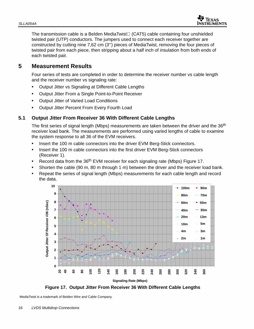
5.1 Output Jitter From Receiver 36 With Different Cable Lengths
The first series of signal length (Mbps) measurements are taken between the driver and the 36th
receiver load bank. The measurements are performed using varied lengths of cable to examinethe system response to all 36 of the EVM receivers.
• Insert the 100 m cable connectors into the driver EVM Berg-Stick connectors.• Insert the 100 m cable connectors into the first driver EVM Berg-Stick connectors
(Receiver 1).• Record data from the 36th EVM receiver for each signaling rate (Mbps) Figure 17.• Shorten the cable (90 m, 80 m through 1 m) between the driver and the receiver load bank.• Repeat the series of signal length (Mbps) measurements for each cable length and record
the data.
80m 70m
60m 50m
40m 30m
20m 13m
10m 5m
4m 3m
2m 1m
0
1
2
3
4
5
6
7
8
9
10
100
120
140
160
180
200
220
240
260
280
300
320
340
360
Signaling Rate (Mbps)
Out
put J
itter
Of R
ecei
ver
#36
(nS
ec)
100m 90m
80604020
Figure 17. Output Jitter From Receiver 36 With Different Cable Lengths
MediaTwist is a trademark of Belden Wire and Cable Company.

SLLA054A
17 LVDS Multidrop Connections
The results of the tests are presented in Figure 17 and clearly show that output jitter isproportional to cable length, but the data format is not in the conventional format for percentjitter. In Figure 18 the same data is replotted as percent jitter.
0
10
20
30
40
50
60
70
80
90
100
20 50 80 110 140 170 200 230 260 290 320 350
Signaling Rate (Mbps)
Out
put J
itter
(%
) O
f Rec
eive
r #3
6100m
90m
80m
70m
60m
50m
40m
30m
20m
13m
10m
5m
4m
3m
2m
1m
Figure 18. Output Jitter vs Signaling Rate at Different Cable Lengths
5.2 Output Jitter From a Single Point-to-Point Receiver
The second series of signal length (Mbps) measurements are taken between the driver and the36th EVM receiver only. The measurements are performed using varied lengths of cable toexamine the system response to the 36th EVM receiver only.
• Remove the jumper wires between the 35th and 36th EVM receivers.
• Insert the 30 m cable connectors into the driver EVM Berg-Stick connectors.
• Insert the 30 m cable connectors into the 36th EVM receiver Berg-Stick connectors.
• Record data from the 36th EVM receiver for each signaling rate (Mbps) Figure 19.
• Shorten the cable (10 m, 3 m, and 1 m) between the driver and the 36th EVM receiver.
• Repeat the series of signal length (Mbps) measurements for each cable length and recordthe data.
The results of the tests are presented in Figure 18.

SLLA054A
18 LVDS Multidrop Connections
0
10
20
30
40
50
60
70
100
115
130
145
160
175
190
205
220
235
250
265
280
295
310
325
Signaling Rate (Mbps)
Out
put J
itter
(%
)30m and 1 Drop10m and 1 Drop3m and 1 Drop1m and 1 Drop
Figure 19. Output Jitter From a Single Point-to-Point Receiver
5.3 Output Jitter of Varied Load Conditions
The third series of signal length (Mbps) measurements are taken between the driver and variedEVM receiver load drops. The measurements are performed using varied lengths of cable toexamine the system response to the varied EVM receiver load drops.
• Remove the jumper wire between the ninth and tenth EVM receivers.
• Insert the 30 m cable connectors into the driver EVM Berg-Stick connectors.
• Insert the 30 m cable connectors into the ninth EVM receiver Berg-Stick connectors.
• Record data from the ninth EVM receiver for each signaling rate (Mbps) Figure 20.
• Shorten the cable (10 m, 3 m, and 1 m) between the driver and the ninth EVM receiver.
• Repeat the series of signal length (Mbps) measurements for each cable length and recordthe data.
• Remove the jumper wire between the 18th and 19th EVM receivers.
• Insert the 30 m cable connectors into the driver EVM Berg-Stick connectors.
• Insert the 30 m cable connectors into the 18th EVM receiver Berg-Stick connectors.
• Record data from the 18th EVM receiver for each signaling rate (Mbps) Figure 21.
• Shorten the cable (10 m, 3 m, and 1 m) between the driver and the 18th EVM receiver.
• Repeat the series of signal length (Mbps) measurements for each cable length and recordthe data.
• Remove the jumper wire between the 27th and 28th EVM receivers.
• Insert the 30 m cable connectors into the driver EVM Berg-Stick connectors.

SLLA054A
19 LVDS Multidrop Connections
• Insert the 30 m cable connectors into the 27th EVM receiver Berg-Stick connectors.
• Record data from the 27th EVM receiver for each signaling rate (Mbps) Figure 22.
• Shorten the cable (10 m, 3 m, and 1 m) between the driver and the 27th EVM receiver.
• Repeat the series of signal length (Mbps) measurements for each cable length and recordthe data.
The results of the tests are presented in Figures 20, 21, and 22.
0
10
20
30
40
50
60
70
Out
put J
itter
(%
)
30m and 9 Drops
10m and 9 Drops
3m and 9 Drops
1m and 9 Drops
Signaling Rate (Mbps)
100
110
120
130
140
150
160
180
190
200
210
170
220
230
240
250
260
270
280
290
300
310
320
330
Figure 20. Output Jitter of a Nine Receiver Load Bank
0
10
20
30
40
50
60
70
Signaling Rate (Mbps)
Out
put J
itter
(%
)
30m and 18 Drops
10m and 18 Drops
3m and 18 Drops
1m and 18 Drops
100
110
120
130
140
150
160
180
190
200
210
170
220
230
240
250
260
270
280
290
300
310
320
330
Figure 21. Output Jitter of an Eighteen Receiver Load Bank
SLLA054A
20 LVDS Multidrop Connections
0
10
20
30
40
50
60
70
Signaling Rate (Mbps)
Out
put J
itter
(%
)30m and 27 Drops10m and 27 Drops3m and 27 Drops1m and 27 Drops
100
110
120
130
140
150
160
180
190
200
210
170
220
230
240
250
260
270
280
290
300
310
320
330
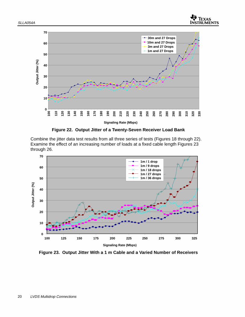
Figure 22. Output Jitter of a Twenty-Seven Receiver Load Bank
Combine the jitter data test results from all three series of tests (Figures 18 through 22).Examine the effect of an increasing number of loads at a fixed cable length Figures 23 through 26.
0
10
20
30
40
50
60
70
100 125 150 175 200 225 250 275 300 325
Signaling Rate (Mbps)
Out
put J
itter
(%
)
1m / 1 drop1m / 9 drops1m / 18 drops1m / 27 drops1m / 36 drops
Figure 23. Output Jitter With a 1 m Cable and a Varied Number of Receivers

SLLA054A
21 LVDS Multidrop Connections
0
10
20
30
40
50
60
70
100 125 150 175 200 225 250 275 300 325
Signaling Rate (Mbps)
Out
put J
itter
(%
)3m / 1 drop3m / 9 drops3m / 18 drops3m / 27 drops3m / 36 drops
Figure 24. Output Jitter With a 3 m Cable and a Varied Number of Receivers
0
10
20
30
40
50
60
70
100 125 150 175 200 225 250 275 300 325
Signaling Rate (Mbps)
Out
put J
itter
(%
)
10m / 1 drop10m / 9 drops10m / 18 drops10m / 27 drops10m / 36 drops
Figure 25. Output Jitter With a 10 m Cable and a Varied Number of Receivers

SLLA054A
22 LVDS Multidrop Connections
0
10
20
30
40
50
60
70
100 125 150 175 200 225 250 275 300 325
Signaling Rate (Mbps)
Out
put J
itter
(%
)
30m / 1 drop30m / 9 drops30m / 18 drops30m / 27 drops30m / 36 drops
Figure 26. Output Jitter With a 30 m Cable and a Varied Number of Receivers
5.4 Percent Output Jitter From Every Fourth Load
The fourth series of signal length (Mbps) measurements are taken first between the driver andthe first EVM receiver only, then from every fourth EVM receiver in the 36 EVM receiver loadbank. The measurements are performed using a 15,24 cm (6′′ ) cable. The HFS-9003 is adjustedfor a signaling rate of 50 Mps, then incremented in 50 Mps steps to 300 Mps, measuring theoutput jitter at each increment.
• Remove the jumper wires between the first and second EVM receivers.
• Insert the six-inch cable connectors into the driver EVM Berg-Stick connectors.
• Insert the six-inch cable connectors into the first EVM receiver Berg-Stick connectors.
• Adjust the HFS-9003 signaling rate to 50 Mps
• Record data from the first EVM receiver for each signaling rate (Mbps) Figure 27.
• Adjust the HFS-9003 signaling rate in increments of 50 Mps, up to 300 Mps, and measurethe output jitter at each increment.
• Connect the jumper wires between the first and second EVM receivers.
• Continue testing every fourth EVM receiver load in the 36 EVM receiver load bank.
The results of the tests are presented in Figure 27.

SLLA054A
23 LVDS Multidrop Connections
0
10
20
30
40
50
60
70
80
90
100
1 4 8 12 16 20 24 28 32 36
Receivers
Out
put J
itter
(%
)50Mbps
100Mbps
150Mbps200Mbps
250Mbps
300Mbps
Figure 27. Percent Output Jitter From Every Fourth Load
6 ConclusionThis report provides basic design guidelines and recommendations for determining operatingmargins, distance between the transmitter and the receivers, and the optimal signaling rates tothe number of LVDS receivers.
6.1 Receiver Number vs Cable Length
While the effect of increased cable length is apparent in Figure 18, performance of the shorterlength cables (30 m) indicates that load number impacts a system as much as cable length. Thisis obvious when the multidrop system plots in Figure 18 are compared with the single pointsystem plots in Figure 19. The point at which each plot crosses the 20% jitter line in Figure 20through Figure 22 clearly demonstrates this increased loading effect.
Not as obvious in Figure 20 through Figure 22 is that the longer cables in these plots appear toboth delay and attenuate reflected signals more than the shorter cables. It appears that althoughcable length increases jitter, length seems to reduce the high and low peaks of the output jittercaused by jumpers and stubs in the load bank. Figure 23 through Figure 26 display thisunexpected characteristic with a decrease in the dramatic fluctuations of the 1 m and 3 m plots,on the 10 m and 30 m plots. The longer cables effectively smooth out the minimum andmaximum peaking evident in the shorter lengths, however overall performance of the system stilldegrades rapidly with increased cable length.
Figure 27 illustrates the fact that data taken at the last receiver (EVM #36), does not representthe worst case jitter in the load bank. It appears that the stub lengths and connectors along theload contribute noise and jitter to the system, but the fact that the slope is negative betweenloads 32 and 36 implies that the termination at the last load attenuates jitter. The positive slopeof the first four loads (except at 200 Mbps) indicates that the cable and driver also attenuatesystem jitter generated along the load bank. These effects are amplified in the higher signalingrates.

SLLA054A
24 LVDS Multidrop Connections
0
10
20
30
40
50
60
70
80
1 3 5 7 9 11 13 15 17 19 21 23 25 27 29 31 33 35
Load
Out
put J
itter
(%
)300
250
200
150
100
50
Poly. (50)
Figure 28. Percent Output Jitter From Each Multidrop Load
An examination of possible attenuation by the transmission cable and driver with a 1 m cable isrecorded in Figure 28 as the output jitter from each load. These results again present a positiveslope at the beginning of the load bank and a negative slope at the end. While a gradual noiseincrease is expected with an increase in cable length, clearly this extra noise is being generatedby the stub and connectors along the load bank.
It is also apparent that jitter levels shift along the load bank as the signaling rate is changed,establishing a characteristic wave of the load bank. The number of loads and the propagationdelays introduced by the cables between receivers directly influence this wave, which in the testsetup are the 7,62 cm (3′′ ) jumpers between EVMs. Based on these results, measurements ofthe propagation delay are made across the entire load bank. The fundamental and harmonicsignaling rates related to this delay are examined.
A delay of 20.9 ns is measured from the output of the first receiver (#1) to the output of the lastreceiver (now #35 since the receiver output pins on one of the loads was damaged during theprevious test). This 20.9 ns delay equates to a characteristic signaling rate of 47 Mbps (1/21 ns),and a third harmonic of 141 Mbps. If a standing wave is being generated along the load bank,then this wave should shift along the load bank as the signaling rate is changed.
Increasing the signaling rate in quarter-wave increments of 12 Mbps, the next series of tests areperformed with an initial signaling rate of the third harmonic. The second test is performed withthe signaling rate increased to 155 Mbps, then increased again to 167 Mbps, and finally 179Mbps. The results are plotted with third order poly nominal trend lines in Figure 29, employed toexamine the wave more clearly.
Next, the load bank is reconfigured to approximate the same characteristic wave using half thenumber of receivers (#19 – #36) and doubling the line length between EVMs from 7,62 cm (3′′ )to 15,24 cm (6′′ ), using a 1 m cable from the driver to EVM #19. This should create a load bankof 18 receivers with a propagation delay somewhere near the original.

SLLA054A
25 LVDS Multidrop Connections
The delay between the output of the first load (#19) and the last load (#36) is 17.2 ns,corresponding to a characteristic rate of 58 Mbps. As done previously, the third harmonic withquarter wavelength increases in the signaling rate are now applied to the driver, with resultsplotted in Figure 30.
0
500
1000
1500
2000
2500
1 4 7 10 13 16 19 22 25 28 31 34
Out
put J
itter
(pS
ec)
143Mbps
155 Mbps
167Mbps
179Mbps
Load
Figure 29. Percent Output Jitter From a 35 Drop 21 ns Load
0
500
1000
1500
2000
2500
3000
19 21 23 25 27 29 31 33 35
Load
Out
put J
itter
(pS
ec)
159.0Mbps 173.5Mbps
188.0Mbps 202.5Mbps
159.0Mbps 3rd Order Trend 173.5Mbps 3rd Order Trend
188.0Mbps 3rd Order Trend 202.5Mbps 3rd Order Trend
Figure 30. Output Jitter From an 18-Receiver 17.1 ns Load
The wave, generated by reflections from connectors and stubs present on each EVM, shiftsalong the load bank as a function of the signaling rate. The output jitter of the first load is not theworst case, and the output jitter from the last load may not be the worst case in a system.

SLLA054A
26 LVDS Multidrop Connections
A closer examination of another source of jitter is made at the termination resistor, across theinputs of the last receiver in the load. As expected, the rise and fall times of the signal are muchfaster with this 18-receiver load bank than with the 36-receiver load bank. To analyze thisapparent signal decay more closely, the short 7,62 cm (3′′ ) jumpers are reinstalled across the35-receiver loads and a 500-Ω series resistor is added in series with the bank on a short cablefrom the driver. The 100-Ω termination resistor is removed to effectively measure the timeconstant of the signal decay.
The HFS-9003 is adjusted for a 1 Vp-p 1-kHz pulse and applied to the driver input. The decaytime of the signal is measured across the receiver inputs of the last load; this decay time dividedby the 500-Ω resistance results in a total value of 640 pF for the entire bank. This breaks downto just over 18 pF (640/35) for each EVM and jumper, and it increases to 20 pF with the long15,24 cm (6′′ ) jumpers installed.
Increased capacitance causes slower rise and fall times, therefore the time that edges are withina receiver threshold window increases. With this effect, jitter at the input of a receiver ispresented for a longer period of time, then the receiver itself increases this jitter again as anear-linear function of signaling rate (approximately 1 ps of jitter per Mbps).
6.2 Receiver Number vs Signaling Rate
Guidelines for determining the maximum allowable signaling rate that can be used with aparticular number of receivers can now be established. It has already been determined that oneload (EVM and jumper) adds approximately 1 ns of propagation delay and 20 pF of capacitance.Therefore, a plot of propagation delay (# of loads) versus the signaling rate that results in anoutput jitter of 15% becomes a practical design tool. More propagation delay measurements areneeded to complete this graph.
The next series of measurements made on a 13-receiver load (#24 through #36) with 15,24 cm(6′′ ) jumpers, yields a propagation delay of 12.3 ns. Based on the previous results, signalingrates approximately twice the fundamental period, result in jitter levels near 15%, signaling ratesof 162 Mbps (2 × 1/12.3 ns) and 142.5 Mbps (1.75 × 1/21.3 ns) for the quarter wavelength shiftare used with results plotted in Figure 31.

SLLA054A
27 LVDS Multidrop Connections
0
2
4
6
8
10
12
14
16
18
20
24 25 26 27 28 29 30 31 32 33 34 35 36
Load
Out
put J
ittte
r (%
)
162.866
142.56162Mbps 3rd Order Trend142Mbps 3rd Order Trend
Figure 31. Output Jitter From a 13-Receiver 12.3 ns Load
The 2x signaling rate yields a peak jitter of 16%. The load bank is increased to 15 receivers anda 14.3 ns load delay is measured. Signaling rates of 140 Mbps (2 × 1/14.3 ns), 157 Mbps (2.24 × 1/14.3 ns), and 175 Mbps (2.5 × 1/14.3 ns) are used for this test. The resulting 2.25xquarter-wave shifted rate of 157 Mbps nearly reaching the 15% jitter mark is shown in Figure 32.
0
5
10
15
20
25
22 23 24 25 26 27 28 29 30 31 32 33 34 35 36
Load
Out
put J
itter
(%
)
175
157.51402.5x 3rd Order Trend2.25x 3rd Order Trend2x 3rd Order Trend
Figure 32. Output Jitter From a 15-Receiver 14.3 ns Load
Remove four jumpers from the load bank to create an 11-drop, 10.4 ns load. When the value ofthe 2x (2 × 1/10.4 ns = 192 Mbps) was recorded, the results were already above 15% jitter.Tests were then made with 1.75x (168 Mbps) and 1.5x (149Mbps) signaling rates. The resultsare shown in Figure 33.

SLLA054A
28 LVDS Multidrop Connections
0
5
10
15
20
25
26 27 28 29 30 31 32 33 34 35 36
Load
Out
put J
itter
(%
)192.308149.233
168.2462x 3rd Order Trend1.5x 3rd Order Trend1.75x 3rd Order Trend
Figure 33. Output Jitter From an 11-Receiver 10.4 ns Load
Tests are repeated with loads of 30, 11, 6, and 3 receivers, and the measurements arecombined with earlier results for the plot in Figure 32. The graph confirms expectations of alinear relationship between propagation delay and a 15% jitter signaling rate. (This graph couldbe titled Load Capacitance vs Signaling Rate.)
The data in Figure 34 may be useful in multidrop system development, if the same constraintsutilized in the test setup are maintained. Stub lengths are 4 cm or less and the single dropcapacitance is approximately 20 pF if the 15,24 cm (6′′ ) cable length between loads is used.The transmission cable from the driver to the receiver bank is 1 m, however, this can be relaxedup to 10 m since there is very little performance difference in cables from 1 m to 10 m length(Figures 18 through 22).

SLLA054A
29 LVDS Multidrop Connections
0
5
10
15
20
25
30
35
100 105 110 115 120 125 130 135 140 145 150 155 160 165 170 175 180 185 190 195 200
Signaling Rate (MB/sec)
Tpd
_Loa
d (n
Sec
)15% Jitter
15% Output Jitter (3rd Order Trend)
Figure 34. Load Propagation Delay vs Signaling Rate
6.3 Receiver Number vs Common-Mode Voltage Range
Earlier this report mentions that the common-mode output current (loc) of an LVDS receiver isnot specified in the LVDS standard, and that as a result the ground potential difference voltage,(Vgpd) may be affected as receivers are added to the output of a single driver. Testing for thiscondition, a third power supply (Tekronix Model PS280) is added to the test setup for monitoringany change in Vgpd. The positive lead of the power supply is connected to the ground of theLVDS31 line driver’s VCC supply, and the negative lead is connected to the ground of the loadbank’s VCC supply. With all jumpers removed from the load bank, the cable from the driver isthen attached to load #36, a single receiver. The signaling rate on the HFS-9003 is set to 100Mbps, and the output of the receiver is monitored while this common-mode voltage is graduallyincreased.
The test is repeated with the addition of each load until all 36 receivers are connected to thesingle driver, then the polarity connections on the PS280 power supply are reversed and thetests repeated.

SLLA054A
30 LVDS Multidrop Connections
–2
–1.5
–1
–0.5
0
0.5
1
1.5
2
1 2 3 4 5 6 7 8 9 10 11 12 13 14 15 16 17 1819 20 21 22 23 24 25 26 2728 29 30 31 32 33 34 35 36
Number of LVDS Loads
100Mbps
200Mbps
Com
mon
Mod
e Vo
ltage
Ran
ge (
Vdo
)
Figure 35. Receiver Number vs Common-Mode Voltage Range
The results presented in Figure 35 confirm that common-mode voltage is impacted by signalingrate. This is due to the gain rolloff of the receiver, and is documented and reported in severalpoint-to-point applications. Also evident in Figure 35 is the increased common-mode loading ofthe receivers linearly loading the 1.2-V common-mode voltage source of the driver, as predictedearlier in the common-mode model discussion.
Clearly the common-mode voltage range decreases as additional receivers are added to theoutput of a single LVDS driver, and as the signaling rate increases.
7 References1. Data sheet, SN65LVDS31 (Literature Number SLLS261)
2. Data sheet, SN65LVDS32 (Literature Number SLLS262)
3. Design note, Low Voltage Differential Signaling (LVDS) Design Notes (Literature NumberSLLA014)
4. Application report, Printed Circuit Board Layout for Improved ElectromagneticCompatibility (Literature Number SDZAE06)
5. Application report, What a Designer Should Know (Literature Number SDZAE03)
6. Seminar manual, Data Transmission Design Seminar (Literature Number SLLDE01)
7. Seminar manual, Digital Design Seminar (Literature Number SDYDE01)
8. Seminar manual, Linear Design Seminar (Literature Number SLYDE05)
9. Paper, Communicate, Issue June 1998
10. LVDS Standard (TIA/EIA – 644)
11. Commercial Building Telecommunications Cabling Standard (ANSI/TIA/EIA–568–A)
12. IEEE 1596.3–1995, Draft Standard for Low-Voltage Differential Signals (LVDS) forScalable Coherent Interfaces (SCI) Draft 1.3

SLLA054A
31 LVDS Multidrop Connections
Appendix A GlossarySignaling Rate: 1/T, where T is the time allocated for one data bit. Therefore, in atransmission system with a 400 Mbps signaling rate, the width of one data bit is 2.5 ns. LVDS,as standardized in TIA/EIA-644, specifies a maximum signaling rate of 655 Mbps, where one bithas a duration of 1.5267 ns. In practice, a maximum signaling rate is determined by the qualityof interconnection between line drivers and receivers, since transmission line length and linecharacteristics ultimately determine the maximum unusable signaling rate. However, theTIA/EIA-644 standard deals with the electrical characteristics of data interchange only, thereforemechanical specifications, bus structure, protocol, and timing are left to the referencingstandard.
Data Rate: The number of data bits per second transmitted from driver to receiver. There arenondata bits, such as start bits, stop bits, parity bits, etc., used by many systems, but they arenot, strictly speaking, actual data bits. If a transmission system is unformatted, and only data bitsare transmitted, then the data rate is equal to the signaling rate.
Jitter: The time frame during which the logic state transition of a signal occurs. The jitter maybe given either as an absolute number or as a percentage with reference to the time unit interval(UI). This UI or bit length equals the reciprocal value of the signaling rate, and the time duringwhich a logic state is valid is just the UI minus the jitter. Percent jitter (the jitter time divided bythe UI times 100) is more commonly used and represents the portion of UI during which a logicstate should be considered indeterminate.
Eye-Pattern: A useful tool for measuring overall signal quality at the end of a transmissionline. It includes all of the effects of systemic and random distortion, and displays the time duringwhich the signal may be considered valid. A typical eye-pattern is illustrated in Figure 12 with itssignificant attributes identified.
Several characteristics of an eye-pattern indicate the signal quality of a transmission circuit. Theheight or opening of the eye above or below the receiver threshold level at the sampling instantis the noise margin of the system. The spread of the transitions across the receiver thresholdsmeasures the peak-to-peak jitter of the data signal. The signal rise and fall times can bemeasured relative to the 0% and 100% levels provided by the series of low and high levels.

IMPORTANT NOTICE
Texas Instruments Incorporated and its subsidiaries (TI) reserve the right to make corrections, modifications,enhancements, improvements, and other changes to its products and services at any time and to discontinueany product or service without notice. Customers should obtain the latest relevant information before placingorders and should verify that such information is current and complete. All products are sold subject to TI’s termsand conditions of sale supplied at the time of order acknowledgment.
TI warrants performance of its hardware products to the specifications applicable at the time of sale inaccordance with TI’s standard warranty. Testing and other quality control techniques are used to the extent TIdeems necessary to support this warranty. Except where mandated by government requirements, testing of allparameters of each product is not necessarily performed.
TI assumes no liability for applications assistance or customer product design. Customers are responsible fortheir products and applications using TI components. To minimize the risks associated with customer productsand applications, customers should provide adequate design and operating safeguards.
TI does not warrant or represent that any license, either express or implied, is granted under any TI patent right,copyright, mask work right, or other TI intellectual property right relating to any combination, machine, or processin which TI products or services are used. Information published by TI regarding third–party products or servicesdoes not constitute a license from TI to use such products or services or a warranty or endorsement thereof.Use of such information may require a license from a third party under the patents or other intellectual propertyof the third party, or a license from TI under the patents or other intellectual property of TI.
Reproduction of information in TI data books or data sheets is permissible only if reproduction is withoutalteration and is accompanied by all associated warranties, conditions, limitations, and notices. Reproductionof this information with alteration is an unfair and deceptive business practice. TI is not responsible or liable forsuch altered documentation.
Resale of TI products or services with statements different from or beyond the parameters stated by TI for thatproduct or service voids all express and any implied warranties for the associated TI product or service andis an unfair and deceptive business practice. TI is not responsible or liable for any such statements.
Mailing Address:
Texas InstrumentsPost Office Box 655303Dallas, Texas 75265
Copyright 2002, Texas Instruments Incorporated