Embed Size (px)
Citation preview

This is an electronic reprint of the original article.This reprint may differ from the original in pagination and typographic detail.
Powered by TCPDF (www.tcpdf.org)
This material is protected by copyright and other intellectual property rights, and duplication or sale of all or part of any of the repository collections is not permitted, except that material may be duplicated by you for your research use or educational purposes in electronic or print form. You must obtain permission for any other use. Electronic or print copies may not be offered, whether for sale or otherwise to anyone who is not an authorised user.
Lyytinen, Jussi; Berdova, Maria; Franssila, Sami; Koskinen, JariAdhesion Testing of Atomic Layer Deposited TiO2 on Glass Substrate by the Use ofEmbedded SiO2 Microspheres
Published in:JOURNAL OF VACUUM SCIENCE AND TECHNOLOGY A
DOI:10.1116/1.4827197
Published: 01/01/2014
Document VersionPublisher's PDF, also known as Version of record
Please cite the original version:Lyytinen, J., Berdova, M., Franssila, S., & Koskinen, J. (2014). Adhesion Testing of Atomic Layer DepositedTiO2 on Glass Substrate by the Use of Embedded SiO2 Microspheres. JOURNAL OF VACUUM SCIENCE ANDTECHNOLOGY A, 32(1), 1-5. [01A102]. https://doi.org/10.1116/1.4827197

Adhesion testing of atomic layer deposited TiO2 on glass substrate by the use ofembedded SiO2 microspheresJussi Lyytinen, Maria Berdova, Sami Franssila, and Jari Koskinen Citation: Journal of Vacuum Science & Technology A 32, 01A102 (2014); doi: 10.1116/1.4827197 View online: http://dx.doi.org/10.1116/1.4827197 View Table of Contents: http://scitation.aip.org/content/avs/journal/jvsta/32/1?ver=pdfcov Published by the AVS: Science & Technology of Materials, Interfaces, and Processing Articles you may be interested in Fabrication of high aspect ratio TiO2 and Al2O3 nanogratings by atomic layer deposition J. Vac. Sci. Technol. A 34, 031605 (2016); 10.1116/1.4947586 Microscratch testing method for systematic evaluation of the adhesion of atomic layer deposited thin films onsilicon J. Vac. Sci. Technol. A 34, 01A124 (2016); 10.1116/1.4935959 Structural properties of as deposited and annealed ZrO2 influenced by atomic layer deposition, substrate, anddoping J. Vac. Sci. Technol. A 31, 01A119 (2013); 10.1116/1.4765047 Nanoscratch testing of atomic layer deposition and magnetron sputtered TiO2 and Al2O3 coatings on polymericsubstrates J. Vac. Sci. Technol. A 30, 01A132 (2012); 10.1116/1.3665418 Improved nucleation of TiN atomic layer deposition films on SiLK low-k polymer dielectric using an Al 2 O 3atomic layer deposition adhesion layer J. Vac. Sci. Technol. B 21, 1099 (2003); 10.1116/1.1577568
Redistribution subject to AVS license or copyright; see http://scitation.aip.org/termsconditions. IP: 130.233.138.192 On: Fri, 08 Jul 2016 10:28:21

Adhesion testing of atomic layer deposited TiO2 on glass substrateby the use of embedded SiO2 microspheres
Jussi Lyytinena)
Department of Materials Science and Engineering, Aalto University, P.O. Box 16200, Aalto 00076, Finland
Maria Berdova and Sami FranssilaDepartment of Materials Science and Engineering and Micronova Nanofabrication Center, Aalto University,P.O. Box 13500, Aalto 00076, Finland
Jari KoskinenDepartment of Materials Science and Engineering, Aalto University, P.O. Box 16200, Aalto 00076, Finland
(Received 9 August 2013; accepted 15 October 2013; published 29 October 2013)
In this paper, the authors present a new adhesion test method, which is under development, to study
the interfacial mechanical parameters of atomic layer deposited (ALD) thin films. A highly sensitive
lateral force adhesion testing tool was used to measure the lateral detaching force of 8 lm diameter
SiO2 microspheres embedded in 100 nm ALD TiO2 thin film grown in 200 �C. The resulting holes in
the coating were characterized with scanning electron microscope plus energy dispersive x-ray
spectroscopy and the delaminated areas were measured with image analysis software. The
corresponding detaching force (F) was compared to the delaminated area (A) to calculate the critical
stress value (r), which relates to the mechanical adhesion of the coating and also includes the effect
of other influencing factors such as the film cohesion. The measured critical stress (r) of the ALD
TiO2 coating on a glass substrate was 36 6 12 MPa based on the measurement of 43 microspheres.VC 2014 American Vacuum Society. [http://dx.doi.org/10.1116/1.4827197]
I. INTRODUCTION
Ultrathin films down to one atomic layer thickness can be
produced by atomic layer deposition (ALD) with high con-
formality and excellent thickness control.1 ALD thin films
are typically used in silicon-based electronics and microelec-
tromechanical systems industry.1–3 Thin film functional
characteristics and performance are highly dependent on suf-
ficient adhesion between the film and the substrate.4
Conventional adhesion testing methods for thin films include
scotch tape testing, scratch-testing, pull-off testing, peel-
testing, bend-testing, to name a few.4–6 There is no universal
technique for determining interfacial toughness. Test-
specific factors and residual stress affect the measured adhe-
sion,4 and the results of all the different adhesion testing
methods are not easily comparable and give qualitative
results at best.7 Conventional adhesion testing of very thin
films in the nanometer range can be problematic; for exam-
ple, during scratch testing, the substrate can break before the
film is delaminated,8 and thus new measurement methods
are needed to test thinner films. New approaches to study the
adhesion behavior of atomic layer deposited thin films
include shaft-loading blister testing9 and scanning nano-
wear.8 Matoy et al. studied interface fracture properties of
silicon oxide and metallic thin films by deflecting microcan-
tilevers fabricated by focused ion beam machining10 that has
similar test geometry as our embedded microsphere test
structure.
In this paper, we present a new adhesion test method which
is under development, where microspheres embedded into an
ALD coating are detached and the resulting delaminated area
is compared to the detaching load to define critical stress
value related to mechanical adhesion. More specifically, the
adhesion of 100 nm ALD TiO2 thin film to glass substrate is
measured by detaching embedded 8 lm SiO2 microspheres
with NanoGalax11 CellAdhesion lateral force testing equip-
ment and defining the delaminated area with scanning elec-
tron microscope (SEM) and digital image analysis.
II. EXPERIMENT
SiO2 microspheres in an ethanol dispersion were depos-
ited and embedded in ALD titania (TiO2) thin film on a glass
substrate. The spheres were detached with NanoGalax
CellAdhesion testing equipment [Fig. 1(a)] with a custom
micromachined tip having a tungsten wire glued to it [sche-
matic presentation in Fig. 1(b)] to accurately target individ-
ual microspheres. The resulting holes in the coating were
characterized with SEM, and the delaminated areas were
measured with ImageJ digital image analysis software.12
A. Sample fabrication
SiO2 microspheres with the vendor specified average diam-
eter of 8 lm (with a coefficient of variation <10%) purchased
from Cospheric LLC were dispersed and ultrasonicated in
ethanol to create a 0.005% w/v solution with a good disper-
sion. A droplet of the dispersion was deposited and dried on a
glass substrate (Menzel-Gl€aser microscope slides with 72.2%
SiO2, 14.3% Na2O, 6.4% CaO, 4.3% MgO, 1.2% K2O, 1.2%
Al2O3, 0.3% SO3, and 0.03% of Fe2O3).
The microspheres were embedded in 100 nm ALD TiO2
deposited at 200 6 5 �C from TiCl4 and H2O precursors
using Beneq-TFS500 reactor at Micronova Nanofabrication
Center of Aalto University. The following deposition cyclesa)Electronic mail: [email protected]
01A102-1 J. Vac. Sci. Technol. A 32(1), Jan/Feb 2014 0734-2101/2014/32(1)/01A102/5/$30.00 VC 2014 American Vacuum Society 01A102-1
Redistribution subject to AVS license or copyright; see http://scitation.aip.org/termsconditions. IP: 130.233.138.192 On: Fri, 08 Jul 2016 10:28:21

were used: TiCl4 pulse and purge (waiting time 200 ms,
pulse 300 ms, waiting time 500 ms, and purge 1.5 s), H2O
pulse and purge (waiting time 200 ms, pulse 240 ms, waiting
time 700 ms, and purge 1.5 s) with a deposition rate of
0.425 A/cycle. The final structure of the embedded spheres
in the coating can be seen in Figs. 2 and 3(a).
B. Measurement with lateral force adhesion tester
Adhesion measurement was carried out by detaching the
embedded microspheres using NanoGalax CellAdhesion
lateral force adhesion tester [Fig. 1(a)] with a custom micro-
machined tip having a 15 lm tungsten wire glued to the end
of the tip. The tip module was calibrated before the measure-
ment with proprietary NanoGalax methods. In Fig. 2 is a
view of the optical microscope measurement including the
tungsten wire attached to the tip on the lower left corner.
The critical stress r (MPa) was defined as the detachment
force F (lN) divided by the delaminated area A (lm2).
C. Characterization with SEM 1 EDS and digital imageanalysis
The sample was characterized with Hitachi 4700 FE-
SEM before [Fig. 3(a)] and after [Fig. 3(b)] the lateral force
measurement. Forty-three microspheres were identified and
their coordinates were recorded to find each individual
sphere before and after the measurement. Energy dispersive
x-ray spectroscopy (EDS) was used to confirm delamination
of the coating by comparing the elements found in the hole
and in the coating. The delaminated area of the resulting
hole was masked with Adobe Photoshop, and the area was
measured with ImageJ digital image analysis software.
III. RESULTS AND DISCUSSION
A. EDS analysis
Besides visual observation in SEM, EDS analysis was used
to confirm coating delamination (Fig. 4), and the results can be
found in Table I. EDS analysis from the film area (spectrum 1
FIG. 1. (Color online) (a) Lateral force adhesion testing tool. (b) Schematic
presentation of the measurement tip. The micromachined tip has a 15lm
tungsten wire attached at the end of the tip that is used to accurately detach
individual spheres while measuring the lateral force required for detachment.
FIG. 2. Optical microscope view of the measurement. The tungsten wire
attached to the tip can be seen in the lower left corner.
FIG. 3. (a) Microsphere before measurement. (b) The resulting hole after
measurement. SEM image is tilted 45�.
01A102-2 Lyytinen et al.: Adhesion testing of ALD TiO2 on glass substrate 01A102-2
J. Vac. Sci. Technol. A, Vol. 32, No. 1, Jan/Feb 2014
Redistribution subject to AVS license or copyright; see http://scitation.aip.org/termsconditions. IP: 130.233.138.192 On: Fri, 08 Jul 2016 10:28:21

in Fig. 4 and Table I) resulted in a Titanium signal of 13 wt.
%, whereas EDS analysis from the hole area (spectrums 2 and
3 in Fig. 4 and Table I) resulted in no titanium signal at all,
confirming that the film had been delaminated.
B. SEM characterization for area calculation anddigital image analysis
After the SEM characterization three main mechanisms
were observed that consume energy during the detaching of
the spheres: film–substrate interfacial failure [Fig. 5(a)],
film-sphere interfacial failure [Fig. 5(b)], and cohesive fail-
ure (breakage of the film that can be seen as the edges of the
hole in the coating in Fig. 5).
For each microsphere, the area of each specific mechanism
was calculated by masking the specific areas with Adobe
Photoshop and calculating the masked areas by ImageJ digital
image analysis software. One of the masking results is shown
in Figs. 6(a)–6(d), where Fig. 6(a) shows the original SEM
image, Fig. 6(b) shows the area of film–substrate interfacial
failure, Fig. 6(c) shows the area of film-sphere interfacial fail-
ure, and Fig. 6(d) shows the area of cohesive failure (breakage
of the film).
C. Critical stress measurement results
The samples were divided into three groups according to
the major failure mechanism: In group 1, the delamination
occurred mostly from the film–substrate interface seen in
Fig. 5(a), in group 2 delamination occurred mostly from the
film–sphere interface seen in Fig. 5(b), and in group 3,
the delamination occurred from both interfaces (having
mixed modes of interfacial failure with no clear dominating
failure mechanism). The critical stress measurement results
from detaching the spheres for each group can be found in
Table II. The critical stress values (r) are plotted for all
TABLE I. EDS analysis results (in wt. %) from the film area (spectrum 1) and
from the hole area (spectrums 2 and 3). Comparison of Ti signal between
the film area (13 wt. %) and the hole area (no signal) confirmed that the film
had been delaminated.
Spectrum O Na Mg Al Si K Ca Ti Total
Spectrum 1 44.32 5.3 1.89 0.43 31.18 3.51 13.37 100
Spectrum 2 44.56 7.25 2.16 0.52 40 0.51 5.01 100
Spectrum 3 45.82 5.83 2.23 0.57 40.69 4.86 100
FIG. 5. (a) Film–substrate interfacial failure (delamination). (b) Film–sphere
interfacial failure. Cohesive failure (breakage of the film) can be observed at
the edge of the hole in the coating.
FIG. 4. (Color online) EDS analysis was done to confirm delamination of the
ALD titania coating. Spectrum 1 is from the film area. Spectrums 2 and 3
are from the delaminated area.
FIG. 6. Definition of different areas for each failure mechanism with digital
image analysis. (a) Original SEM image. (b) Masked area for film–substrate
delamination area calculation. (c) Masked area for film–sphere delamination
area calculation. (d) Masked area for cohesive failure area calculation. The
total area of delamination is the combined area of (b)–(d).
01A102-3 Lyytinen et al.: Adhesion testing of ALD TiO2 on glass substrate 01A102-3
JVST A - Vacuum, Surfaces, and Films
Redistribution subject to AVS license or copyright; see http://scitation.aip.org/termsconditions. IP: 130.233.138.192 On: Fri, 08 Jul 2016 10:28:21
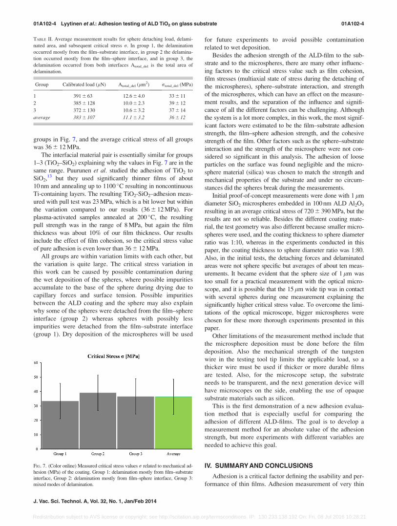
groups in Fig. 7, and the average critical stress of all groups
was 36 6 12 MPa.
The interfacial material pair is essentially similar for groups
1–3 (TiO2–SiO2) explaining why the values in Fig. 7 are in the
same range. Puurunen et al. studied the adhesion of TiO2 to
SiO2,13 but they used significantly thinner films of about
10 nm and annealing up to 1100 �C resulting in noncontinuous
Ti-containing layers. The resulting TiO2-SiO2–adhesion meas-
ured with pull test was 23 MPa, which is a bit lower but within
the variation compared to our results (36 6 12 MPa). For
plasma-activated samples annealed at 200 �C, the resulting
pull strength was in the range of 8 MPa, but again the film
thickness was about 10% of our film thickness. Our results
include the effect of film cohesion, so the critical stress value
of pure adhesion is even lower than 36 6 12 MPa.
All groups are within variation limits with each other, but
the variation is quite large. The critical stress variation in
this work can be caused by possible contamination during
the wet deposition of the spheres, where possible impurities
accumulate to the base of the sphere during drying due to
capillary forces and surface tension. Possible impurities
between the ALD coating and the sphere may also explain
why some of the spheres were detached from the film–sphere
interface (group 2) whereas spheres with possibly less
impurities were detached from the film–substrate interface
(group 1). Dry deposition of the microspheres will be used
for future experiments to avoid possible contamination
related to wet deposition.
Besides the adhesion strength of the ALD-film to the sub-
strate and to the microspheres, there are many other influenc-
ing factors to the critical stress value such as film cohesion,
film stresses (multiaxial state of stress during the detaching of
the microspheres), sphere–substrate interaction, and strength
of the microspheres, which can have an effect on the measure-
ment results, and the separation of the influence and signifi-
cance of all the different factors can be challenging. Although
the system is a lot more complex, in this work, the most signif-
icant factors were estimated to be the film–substrate adhesion
strength, the film–sphere adhesion strength, and the cohesive
strength of the film. Other factors such as the sphere–substrate
interaction and the strength of the microsphere were not con-
sidered so significant in this analysis. The adhesion of loose
particles on the surface was found negligible and the micro-
sphere material (silica) was chosen to match the strength and
mechanical properties of the substrate and under no circum-
stances did the spheres break during the measurements.
Initial proof-of-concept measurements were done with 1 lm
diameter SiO2 microspheres embedded in 100 nm ALD Al2O3
resulting in an average critical stress of 720 6 390 MPa, but the
results are not so reliable. Besides the different coating mate-
rial, the test geometry was also different because smaller micro-
spheres were used, and the coating thickness to sphere diameter
ratio was 1:10, whereas in the experiments conducted in this
paper, the coating thickness to sphere diameter ratio was 1:80.
Also, in the initial tests, the detaching forces and delaminated
areas were not sphere specific but averages of about ten meas-
urements. It became evident that the sphere size of 1lm was
too small for a practical measurement with the optical micro-
scope, and it is possible that the 15 lm wide tip was in contact
with several spheres during one measurement explaining the
significantly higher critical stress value. To overcome the limi-
tations of the optical microscope, bigger microspheres were
chosen for these more thorough experiments presented in this
paper.
Other limitations of the measurement method include that
the microsphere deposition must be done before the film
deposition. Also the mechanical strength of the tungsten
wire in the testing tool tip limits the applicable load, so a
thicker wire must be used if thicker or more durable films
are tested. Also, for the microscope setup, the substrate
needs to be transparent, and the next generation device will
have microscopes on the side, enabling the use of opaque
substrate materials such as silicon.
This is the first demonstration of a new adhesion evalua-
tion method that is especially useful for comparing the
adhesion of different ALD-films. The goal is to develop a
measurement method for an absolute value of the adhesion
strength, but more experiments with different variables are
needed to achieve this goal.
IV. SUMMARY AND CONCLUSIONS
Adhesion is a critical factor defining the usability and per-
formance of thin films. Adhesion measurement of very thin
FIG. 7. (Color online) Measured critical stress values r related to mechanical ad-
hesion (MPa) of the coating. Group 1: delamination mostly from film–substrate
interface, Group 2: delamination mostly from film–sphere interface, Group 3:
mixed modes of delamination.
TABLE II. Average measurement results for sphere detaching load, delami-
nated area, and subsequent critical stress r. In group 1, the delamination
occurred mostly from the film–substrate interface, in group 2 the delamina-
tion occurred mostly from the film–sphere interface, and in group 3, the
delamination occurred from both interfaces Atotal_del is the total area of
delamination.
Group Calibrated load (lN) Atotal_del (lm2) rtotal_del (MPa)
1 391 6 63 12.6 6 4.0 33 6 11
2 385 6 128 10.0 6 2.3 39 6 12
3 372 6 130 10.6 6 3.2 37 6 14
average 383 6 107 11.1 6 3.2 36 6 12
01A102-4 Lyytinen et al.: Adhesion testing of ALD TiO2 on glass substrate 01A102-4
J. Vac. Sci. Technol. A, Vol. 32, No. 1, Jan/Feb 2014
Redistribution subject to AVS license or copyright; see http://scitation.aip.org/termsconditions. IP: 130.233.138.192 On: Fri, 08 Jul 2016 10:28:21

films can be challenging, and thus, there is a need for devel-
oping new measurement methods. Often thin film adhesion
is said to be good or bad based on the Scotch tape test, but
no measurable numbers are given. In this paper, we demon-
strate a new adhesion test method especially for ALD thin
films measuring the critical stress to delaminate the film
including the effect of film cohesion. Three main failure
mechanisms were observed, and analysis was made based on
the major failure mechanism. Group 1 events represent
closely the adhesion behavior of the film and the substrate,
and the average critical stress value of TiO2 on a glass sub-
strate was 33 6 11 MPa, which was in the same region and
within the variation limits of all the groups (36 6 12 MPa).
To further develop the new method and get more compara-
tive results, the next steps include the testing of different
film materials, different film thicknesses, depositions done at
different temperatures, and the use of different substrates.
ACKNOWLEDGMENTS
This work has been conducted within the MECHALD
project funded by TEKES (the Finnish Funding Agency for
Technology and Innovation). ALD deposition was done at
the Micronova Nanofabrication Center of Aalto University
by MB. Thanks to Riikka Puurunen and M. Sc. (Tech.) Oili
Ylivaara at VTT Technical Research Center of Finland for
their comments and especially their input in choosing the
coating material and parameters. Thanks to Marko Pudas
and Kristian Jansson at NanoGalax Oy in setting up and
helping with the initial proof-of-concept measurements.
Thanks to M. Sc. (Tech.) Juha Larismaa at Aalto University
for nanoparticle synthesis and Xuwen Liu at Aalto
University for nanomechanical characterization help in prior
research and method development that has led to this paper.
Thanks to M. Sc. (Tech.) Ajai Iyer at Aalto University for
checking the language and for reviewing the contents of the
manuscript.
1S. M. George, Chem. Rev. 110, 111 (2010).2R. L. Puurunen, J. Appl. Phys. 97, 121301 (2005).3R. L. Puurunen, H. Kattelus, T. Suntola, V. Lindroos, M. Tilli, and A.
Lehto, in Handbook of Silicon Based MEMS Materials and Technologies,1st ed., edited by T. Motooka (William Andrew Publishing, Boston,
2010), pp. 433–446.4K. L. Mittal, Electrocomponent Sci. Technol. 3, 21 (1976).5A. A. Volinsky, N. R. Moody, and W. W. Gerberich, Acta Mater. 50, 441
(2002).6R. Lacombe, Adhesion Measurement Methods, Theory and Practice, 1st
ed. (CRC, New York, 2006).7J. Chen and S. J. Bull, J. Phys. D: Appl. Phys. 44, 034001 (2011).8O. M. E. Ylivaara et al., “Aluminum oxide from trimethylaluminum and
water by atomic layer deposition: Residual stress, elastic modulus, hard-
ness and adhesion,” Thin Solid Films (submitted).9M. Berdova, J. Lyytinen, K. Grigoras, A. Baby, L. Kilpi, H.
Ronkainen, S. Franssila, and J. Koskinen, J. Vac. Sci. Technol. A 31,
031102 (2013)10K. Matoy, T. Detzel, M. M€uller, C. Motz, and G. Dehm, Surf. Coat. Tech.
204, 878 (2009)11Nanogalax Oy, Piispanristi, Finland, see: http://www.nanogalax.com/, last
accessed July 20, 2013.12C. A. Schneider, W. S. Rasband, and K. W. Eliceiri, Nat. Methods 9, 671
(2012).13R. L. Puurunen, et al., Sens. Actuators A 188, 268 (2012).
01A102-5 Lyytinen et al.: Adhesion testing of ALD TiO2 on glass substrate 01A102-5
JVST A - Vacuum, Surfaces, and Films
Redistribution subject to AVS license or copyright; see http://scitation.aip.org/termsconditions. IP: 130.233.138.192 On: Fri, 08 Jul 2016 10:28:21


![L. Jetsu, S. Porceddu, J. Lyytinen,P. Kajatkari, J. Lehtinen ...arXiv:1204.6206v2 [astro-ph.SR] 24 May 2013 Draftversion May27,2013 Preprint typeset using LATEX style emulateapj v](https://img.pdfslide.net/doc/110x75/604dd9398de2302d3c59535f/l-jetsu-s-porceddu-j-lyytinenp-kajatkari-j-lehtinen-arxiv12046206v2.jpg)