Embed Size (px)
Citation preview

Progress of 2- m Detectors for
Application to Lidar Remote Sensing
LaRC
M. Nurul AbedinRemote Sensing Flight Systems Branch NASA Langley Research Center MS 468, 5 N. Dryden Street Hampton, VA 23681
Tamer Refaat Old Dominion University
Syed Ismail Science Directorate
Grady KochLaser Remote Sensing Branch/SED
Upendra Singh Systems Engineering Directorate

OutlineLaRC
Progress of 2- m Detectors for ………
• Overview• Objective• Applications• Detector Characterization at Langley• Custom-Designed Detector Validation• Summary

Overview
• Detector with high gain and low noise is a detector of choice for laser remote sensing applications and no commercial detector was available at 2-μm wavelength range.
• NASA Langley Research Center’s detector group worked in collaboration with Astro-Power, Inc./University of Delaware to develop custom-designed 2-micron phototransistors using Liquid Phase Epitaxy (LPE) technique.
• These phototransistors have very high gain, but also have longer recovery time, which may cause problem for CO2 DIAL applications.
• Raytheon achieved high gain, high speed, and ultra low excess noise factor around 1 from the Avalanche Photodiode.
• Therefore, NASA Langley acquired HgCdTe avalanche photodiodes (APD) from Raytheon, characterized and applied in atmospheric testing at 2-μm.
LaRC
Progress of 2- m Detectors for ………

Develop, test, and implement new technology 2 μm detectorsfor application to laser remote sensing from ground, aircraft,and space.
ObjectiveLaRC
Progress of 2- m Detectors for ………

2-μm Detector Applications
• Detectors with responsivity at broad wavelengths areneeded to span a wide wavelength range for the followingapplications
CO2, O3, H2O, and CH4
aerosols and clouds detection of a large number of species in the
visible-near infrared using active and passive remote sensing techniques, and
enable new science and lower-cost missions through compact instruments
LaRC
Progress of 2- m Detectors for ………
2-μm Detectors Development and Characterization
Single element custom-designed phototransistors and avalanchephotodiodes have been developed at Astropower/University ofDelaware and Raytheon Vision Systems; and characterized themat NASA Langley Research Center
Measured the phototransistor’s responsivity and noiseDetermined device performances, such as detectivity and noise
equivalent powerDemonstrated high responsivity 2650 A/W corresponding to an
internal gain of 2737High detectivity (D*) 3.9x1011 cm.Hz /W that is equivalent to
a noise equivalent power of 4.6x10⁻¹⁴ W/Hz .
Evaluated the APD’s spectral response Determined high quantum efficiency and high gain
LaRC
Progress of 2- m Detectors for ………

LaRC
Progress of 2- m Detectors for ………
Detector Calibration

Custom-Designed Detector Calibration
2 μm InGaAsSb Phototransistor Characteristics
Custom-designed 2 m Detector Technology
T.F. Refaat, M.N. Abedin, O.V. Sulima, S. Ismail, and U.N. Singh, “AlGaAsSb/InGaAsSb Phototransistors for 2- m Remote Sensing Applications”, Optical Engineering, Vol. 43(7), 1647-1650, 2004.
• PbS Reference Detector• 20 nm Spectral Resolution• -20 to 20 oC Temperature• Different Bias Voltages• Calculated Quantum Efficiency
for 0 V at 20 oC
0
10
20
30
40
50
60
0
10
20
30
40
50
60
1000 1200 1400 1600 1800 2000 220010
-2
10-1
100
101
102
103
104
Wavelength [nm]
Res
po
nsi
vity
[A
/W]
Qu
an
tum
Eff
icie
ncy
[%
]
0.0 V, 20 oC
1.0 V, 20 oC
2.0 V, 20 oC
3.0 V, 20 oC
3.5 V, -20 oC
4.0 V, -20 oC4.4 V, -20 oC
0
10
20
30
40
50
60
0
10
20
30
40
50
60
1000 1200 1400 1600 1800 2000 220010
-210
-2
10-1
10-1
100
100
101
101
102
102
103
103
104
104
Wavelength [nm]
Res
po
nsi
vity
[A
/W]
Qu
an
tum
Eff
icie
ncy
[%
]
0.0 V, 20 oC
1.0 V, 20 oC
2.0 V, 20 oC
3.0 V, 20 oC
3.5 V, -20 oC
4.0 V, -20 oC4.4 V, -20 oC
LaRC
Progress of 2- m Detectors for ………

LaRC
Progress of 2- m Detectors for ………
InGaAsSb detector peak positions shifted due to temperature variation
• PbS Reference Detector• 20 nm Spectral Resolution• -193 to 70 oC Temperature• Different Bias Voltages (0 V to 5 V)
Custom-designed 2 m Detector Technology
M.N. Abedin, T.F. Refaat, O.V. Sulima, and U.N. Singh, “Recent development of Sb-based phototransistors in the 0.9- to 2.2- m wavelength range for applications to laser remote sensing”, International Journal of High Speed Electronics and Systems, v.15, No.2, pp. 567-582, (2006).
600 1000 1400 1800 220010-2
100
102
104
Wavelength [nm]
Res
po
nsi
vit
y [
A/W
]
20oC & 0V
20oC & 4V 70oC & 2V
-193oC & 0V
-193oC & 5V
600 1000 1400 1800 220010-2
100
102
104
Wavelength [nm]
Res
po
nsi
vit
y [
A/W
]
20oC & 0V
20oC & 4V 70oC & 2V
-193oC & 0V
-193oC & 5V
Custom-Designed Detector Calibration
2 μm InGaAsSb Phototransistor Characteristics

Detector Performance Comparison
Existing and Custom-Designed Phototransistor Characteristics
• With suitable bias voltage and 2-micron radiation, InGaAsSbPhototransistor has the bestdetectivity, compared toInGaAs (I & II) and HgCdTe(III) technologies.
Detectivity (D*)
0 0.5 1 1.5 2 2.5 3 3.5 4
Bias Voltage [V]
1010
1011
1012
D* [
cmH
z1/2
/W]
p-i-n detector I at -20 oC
p-i-n detector II at -20 oC
p-n detector III at -20 oC
Phototransistor at -20 oC
Phototransistor at +20 oC
0 0.5 1 1.5 2 2.5 3 3.5 4
Bias Voltage [V]
1010
1011
1012
D* [
cmH
z1/2
/W]
p-i-n detector I at -20 oC
p-i-n detector II at -20 oC
p-n detector III at -20 oC
Phototransistor at -20 oC
Phototransistor at +20 oC
p-i-n detector I at -20 oC
p-i-n detector II at -20 oC
p-n detector III at -20 oC
Phototransistor at -20 oC
Phototransistor at +20 oC
O.V. Sulima, T.F. Refaat, M.G. Mauk, J.A. Cox, J. Li, S.K. Lohokare, M.N. Abedin, U.N. Singh, and J.A. Rand, “AlGaAsSb/InGaAsSb phototransistors for spectral range around 2- m”, Electronics Letters, Vol 40, 766-767, 2004.
LaRC
Progress of 2- m Detectors for ………

10-12
10-11
10-10
μ
μ
μ
μ
μ
G5853
EP
(W
/Hz1
/2)
10-12
10-11
10-10
μ
μ
μ
μ
μ
μ
μ
μ
μ
μ
G5853
EP
(W
/Hz1
/2)
LaRC
Progress of 2- m Detectors for ………
Noise-Equivalent-Power (NEP)
• With suitable bias voltage,InGaAsSb Phototransistor hasthe lowest NEP, compared toInGaAs (G5852: 2.3-cutoff) andInGaAs (G5853: 2.6-cutoff)technologies.
Detector Performance Comparison
Existing and Custom-Designed Phototransistor Characteristics
M.N. Abedin, T.F. Refaat, O.V. Sulima, and U.N. Singh, “AlGaAsSb/InGaAsSb heterojunction phototransistor with high optical gain and wide dynamic range”, IEEE Trans. Electron Devices, Vol. 51(12), pp 2013 - 2018 (2004).

0 1 2 3 4 5 6
100
102
104
106
Bias Voltage [V]
Gain
80.1K
-30oC
+20oC
+70oC
0 1 2 3 4 5 6
100
102
104
106
Bias Voltage [V]
Gain
80.1K
-30oC
+20oC
+70oC
80.1K
-30oC
+20oC
+70oC
LaRC
Progress of 2- m Detectors for ………
Gain
InGaAsSb phototransistor gain variation at different bias voltagefor fixed incident radiation @2.0 m
• Different Temperature.• Bias Voltages (0.0- to5.8-volts).
Determination of Custom-designed 2 m Phototransistor’s Gain
Detector Performance Comparison

LaRC
Quantum Efficiency
2 m Avalanche Photodiode Performance
• Gain at Room and Cryogenic Temperatures with different Bias Voltages
1000 1200 1400 1600 1800 2000 2200 2400 2600 28000
10
20
30
40
50
60
70
80
Wavelength [nm]
QE
[%]
Raytheon 2um APD (B23) Quantum Efficiency
Room Temperature
Cryogenic
0 5 10 150
5
10
15
20
25
Bias Voltage [V]
Gai
n
Raytheon 2um APD (B23) Gain
Room Temperature
Cryogenic
Progress of 2- m Detectors for ………
Gain
• QE at Room and Cryogenic Temperatures with O V Bias Voltage
Note: APD was not AR coated, QE will exceed >80% with AR coating

LaRC
2 m Avalanche Photodiode Performance
Progress of 2- m Detectors for ………
Summary Table of the 2 μm APD
Note: APD was not AR coated, QE will exceed >80% with AR coating; NEP, excess noise factor, and bandwidth are not evaluated

LaRC
Custom-Designed Detector Validation
Validated phototransistors at National Center for AtmosphericResearch (NCAR), Boulder, Colorado, by integrating them intoLidar System operating at 1.543-μm and also at NASA LangleyResearch Center operating at 2.0-μm
Results:• Phototransistor was optimized for 2-μm detection, but its performance is nearly similar to the InGaAs APD at 1.5-μm.
• Lidar tests were performed at 2.0-μm wavelength and results are promising
Progress of 2- m Detectors for ………

• NCAR Lidar operates at 1.5 μm wavelength.• LaRC Lidar operates at 2.0 m wavelength• Lidar serves as a useful test-bed for comparing the phototransistor profile with that of the InGaAs APD• This comparison validates the application of the phototransistor for lidar instruments
Spectral Response & Quantum Efficiency ofPhototransistor
LaRC
Progress of 2- m Detectors for ………

• Obtained lidar backscatter signals through the phototransistor and the InGaAs APD simultaneously• Splitted backscatter signal into two equivalently energetic beams and focused them onto two independent detectors
Courtesy: Schematic of the Lidardetection system at NCAR, Boulder,Colorado, with the phototransistorinstalled into the receiver’s perpendicular
polarization channel.
Transmitter: 170mJ/pulse 4 ns pulse width
Receiver: 40 cm Newtonian Telescope
Phototransistor Validation Setup at NCAR
LaRC
Progress of 2- m Detectors for ………

16:00-16:25; The HPToperating at 20oC with 155mJ/pulse laser energy.
16:30-16:45; Temperature=10oC.
16:50-17:00; Temperature =30oC.
17:10-17:19; Laser energyreduced to 50% applying aneutral density filter to thetransmitted beam (20oC).
Atmospheric Return at 1.5- m
• Color image of the far-field temporal variation of the return signals• Monitoring an optically thin cloud between 4.6 and 5.8 km altitude
LaRC
Progress of 2- m Detectors for ………
LaRC
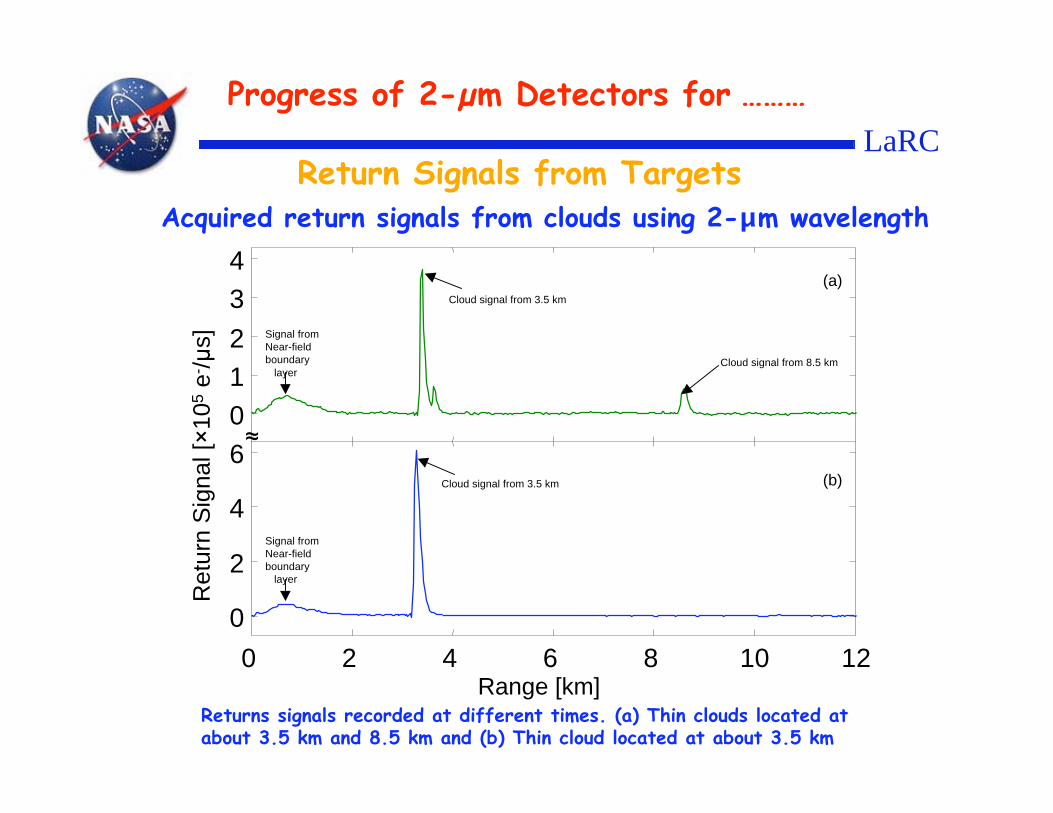
Returns signals recorded at different times. (a) Thin clouds located atabout 3.5 km and 8.5 km and (b) Thin cloud located at about 3.5 km
Return Signals from TargetsAcquired return signals from clouds using 2- m wavelength
Range [km]
0
1
2
3
4
0 2 4 6 8 10 12
0
2
4
6
Retu
rn S
ignal [
10
5 e
- /s]
Signal from
Near-field
boundary
layer
Cloud signal from 3.5 km
Cloud signal from 8.5 km
(a)
(b)Cloud signal from 3.5 km
Signal from
Near-field
boundary
layer
Progress of 2- m Detectors for ………

LaRC
Atmospheric Return at 2-m
• Atmospheric images were obtained using phototransistor at 2-micron• The system was pointed at thin discrete clouds at about 3.5-8.5 km altitudes
The color image from two layers of clouds and boundary-layer The time scale spans between
0 to 550 sec, which corresponds to the phototransistor operating time at a temperature of 20 oC.
Time (s)
Altitude (
m)
3.5 km cloud layer
Near-field
boundary-layer
8.5 km cloud layer100
200
300
400
3.5 km cloud layer
Near-field
boundary-layer
8.5 km cloud layer
100
200
300
400
100
200
300
400
3.5 km cloud layer
Near-field
boundary-layer
8.5 km cloud layer
Progress of 2- m Detectors for ………

LaRCComparison of Atmospheric Returns using 2 m APD from Raytheon and HPT from Astropower
Atmospheric return signals using 2-μm HPT (Top trace) and HgCdTe APD (Bottom trace)
Progress of 2- m Detectors for ………
0 500 1000 1500 2000 2500 3000 3500 4000
0
2
4
6x 10
4
HPT
Range [m]
Sign
al [
V.m
2]
0 500 1000 1500 2000 2500 3000 3500 4000-5
0
5
10
Range [m]
Sign
al [
V.m
2] APD
x 103
0 500 1000 1500 2000 2500 3000 3500 4000
0
2
4
6x 10
4
HPT
Range [m]
Sign
al [
V.m
2]
0 500 1000 1500 2000 2500 3000 3500 4000
0
2
4
6x 10
4
HPT
Range [m]
Sign
al [
V.m
2]
0 500 1000 1500 2000 2500 3000 3500 4000-5
0
5
10
Range [m]
Sign
al [
V.m
2] APD
x 103
0 500 1000 1500 2000 2500 3000 3500 4000-5
0
5
10
Range [m]
Sign
al [
V.m
2] APD
x 103
Range Corrected
Near field
boundary layer
Near field
boundary layer
Note: APD was not optimized for acquiring maximum signal, preliminary results show that APD has good sensitivity without optimization

• Custom-designed phototransistors have been developed at Astropower/UD and characterized at NASA Langley Research Center under LRRP.
• Phototransistor shows comparable performance with respect to InGaAs APD operating at 1.5 m wavelength under lidar testing Results indicated an acceptable performance of the phototransistor
device, in terms of detecting 5 km range atmospheric structures.
• Evaluated the phototransistor’s performances at 2.0- m wavelength Measurements included detecting atmospheric structure consisting
of thin clouds in the mid-altitude and near-field boundary layer.
• Preliminary results indicate that HgCdTe APD has some sensitivity with respect to phototransistor operating at 2.0- m wavelength.
SummaryLaRC
Progress of 2- m Detectors for ………

Acknowledgment
This work is supported by Laser Risk Reduction Program and2- m CO2 DIAL IIP Project under NASA’s Earth ScienceTechnology Office and NASA’s Enabling Concepts &Technologies Program. The authors would like to thanksOleg Sulima from University of Delaware for fabricating thephototransistors and Terry Mack for phototransistorelectronics; Jinxue Wang and Michael Jack from RaytheonVision Systems for APD development; Scott Spuler and ShaneMayor from NCAR to provide lab and also assist to operatethe Lidar System. The authors also acknowledge GeorgeKomar, William Stabnow, and Micheal Kavaya for theirconstant support.
LaRC
Progress of 2- m Detectors for ………