Embed Size (px)
Citation preview
1
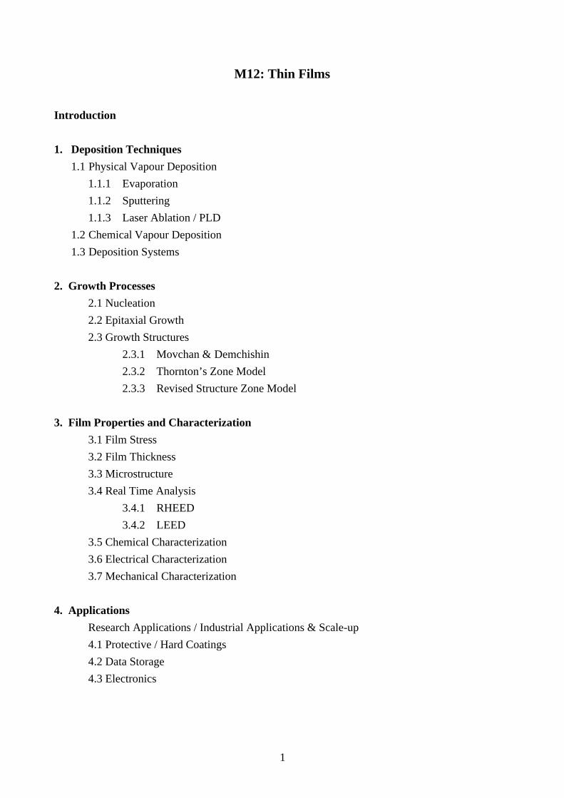
M12: Thin Films
Introduction
1. Deposition Techniques
1.1 Physical Vapour Deposition
1.1.1 Evaporation
1.1.2 Sputtering
1.1.3 Laser Ablation / PLD
1.2 Chemical Vapour Deposition
1.3 Deposition Systems
2. Growth Processes
2.1 Nucleation
2.2 Epitaxial Growth
2.3 Growth Structures
2.3.1 Movchan & Demchishin
2.3.2 Thornton’s Zone Model
2.3.3 Revised Structure Zone Model
3. Film Properties and Characterization
3.1 Film Stress
3.2 Film Thickness
3.3 Microstructure
3.4 Real Time Analysis
3.4.1 RHEED
3.4.2 LEED
3.5 Chemical Characterization
3.6 Electrical Characterization
3.7 Mechanical Characterization
4. Applications
Research Applications / Industrial Applications & Scale-up
4.1 Protective / Hard Coatings
4.2 Data Storage
4.3 Electronics

2
M12 Thin Films
Milton Ohring, The Materials Science of Thin Films (Academic Press,1992, and 2nd edition, 2002)
Nq56
D.L.Smith, Thin Film Deposition, Principles and Practice (McGraw-Hill, 1995) Nq61
Ron Powell and Stephen M. Rossnagel, PVD for Microelectronics (Academic Press,1998) Nq64
Jeffrey A. Hopwood (Ed.), Ionized Physical Vapor Deposition (Academic Press,1999) Nq65
Donald M. Mattox, Handbook of Physical Vapor Deposition (PVD) Processing (Noyes, 1998)
K.-N. Tu, J.W. Mayer and L.C. Feldman, Electronic Thin Film Science for Electrical
Engineers and Materials Scientists (MacMillan, 1992) Nq58
K.K. Schuegraf, Handbook of Thin-Film Deposition Processes and Techniques (Noyes,
1988) Nq54
R.F. Bunshah et al, Deposition Technologies for Films and Coatings (Noyes, 1982; and 2nd edition,
1994) Nq35
J. Sanchez, D.A. Smith and N. Delanerolle, Microstructural Science for Thin Film
Metallizations in Electronic Applications (TMS, 1988) Nq57
E.S. Machlin, Materials Science in Microelectronics (Giro Press, US, 1995) Nq60a
K.L.Chopra and I. Kaur, Thin Film Device Applications (Plenum Press, 1983) Nq37
J. Vossen and W. Kern (eds.), Thin Film Processes (Academic Press, 1978) Nq30
K.J. Klabunde (ed.), Thin Films from Free Atoms and Particles (Academic Press, 1985) Nq41
M. Kunoma, Film Deposition by Plasma Techniques (Springer - Verlag) LcG19
Also:
Vacuum – Ov
Coatings – Qo
Plasmas - LcG
3
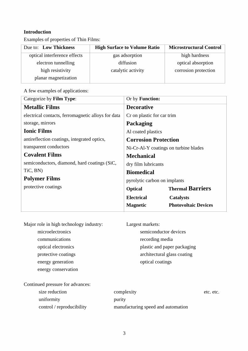
Introduction
Examples of properties of Thin Films:
Due to: Low Thickness High Surface to Volume Ratio Microstructural Control
optical interference effects
electron tunnelling
high resistivity
planar magnetization
gas adsorption
diffusion
catalytic activity
high hardness
optical absorption
corrosion protection
A few examples of applications:
Categorize by Film Type: Or by Function:
Metallic Filmselectrical contacts, ferromagnetic alloys for data
storage, mirrors
Ionic Filmsantireflection coatings, integrated optics,
transparent conductors
Covalent Filmssemiconductors, diamond, hard coatings (SiC,
TiC, BN)
Polymer Filmsprotective coatings
DecorativeCr on plastic for car trim
PackagingAl coated plastics
Corrosion ProtectionNi-Cr-Al-Y coatings on turbine blades
Mechanicaldry film lubricants
Biomedicalpyrolytic carbon on implants
Optical Thermal BarriersElectrical Catalysts
Magnetic Photovoltaic Devices
Major role in high technology industry: Largest markets:
microelectronics
communications
optical electronics
protective coatings
energy generation
energy conservation
semiconductor devices
recording media
plastic and paper packaging
architectural glass coating
optical coatings
Continued pressure for advances:
size reduction complexity etc. etc.
uniformity purity
control / reproducibility manufacturing speed and automation

4
1. Deposition Techniques
1.1 Physical Vapour Deposition
Generation of vapour source Æ transport to substrates Æ nucleation and growth
1.1.1 Evaporation
Supply heat for solid – vapour transition Pv µ exp - D H RT
Need: continuous monitoring, or Energy of evaporated atoms typically ~ 0.1 - 0.3 eV
very accurate temperature control
Resistance Evaporation

5
Electron–beam Evaporation
heat charge directly in hearth Þ high purity, and forreactive materials
Web Coating
Continuous coating, e.g.
videotape
metal on Mylar for capacitors
Al or SiO2 moisture barriers on plastic
multilayer coatings for windows
Alloys
∑ co-evaporation from 2, or more sources
∑ flash evaporation
∑ “special alloys,” compensated for low Pv
component
Heterostructures
Compounds
∑ evaporate directly
(depends on whether they dissociate)
∑ reactive evaporation (e.g. add N2 or O2 for
compound formation)
∑ multiple sources
Uniformity
Assume flux from a point source, or cosine emitter:

6
Activated Reactive Evaporation (ARE): reactive evaporation + source of ionization
Ion Assisted Deposition, Ion Plating: plasma + electrical bias at substrates, or separate ion gun
Molecular Beam Epitaxy (MBE)
Neutral thermal energy beams (molecular or atomic) impinge on a substrate in ultra-high vacuum
∑ molecular beam: m.f.p. > chamber dimension
∑ epitaxy: film derives its crystalline orientation from the substrate
Mean Free Path:
(a) electron in gas, with n molecules per m3
consider molecule as stationary
cross section
=
Þ =
p
lp
d
d ne
2
2
44
(c) another molecule
consider both particles as moving; Þ 2c
lp
= 12 2d n
at 2.5 Pa """" m.f.p. ~ 2.5 mm
(b) ioncross section
=
Þ =
p
lp
d
d ni
2
2
1
e.g. air at room temp.:
Ideal Gas Law P NA = n R T# n ª 3.1025 m-3
d ~ 0.5 nm
# l ~ 50 nm
10-4
10-2
1
100
104
106
108
10-6
mea
n f
ree
pat
h (
m)
Pressure (Pa)
104 100 1 0.01 10-4 10-6 10-8 10-10 10-12
1 mm
1 mm
1 m
1 km
1000 km

7
Knudsen Cell, or Effusion Cell:
Cracker cell - 2 zones; low T (sublimation) + high T (e.g. 800 - 1000°C) (cracking)
$ Deposition onto single crystal substrates at raised temperature (e.g. 0.6 m.pt.)
Þ surface diffusion
$ Ultra-high vacuum
Þ very high purity Þ in situ analysis and real time growth monitoring
∑ Low growth rates; e.g. 1 monolayer s-1
∑ Use substrate rotation for producing uniform films
∑ Use shutters to interrupt deposition instantaneously (e.g. for heterostructures)
- complex
- slow
- expensive Þ limited production applications
- not continuous
- long down times

8
1.1.2. Sputtering
$ sputtered flux mainly atoms with energies of a few eV – a few 10s eV (random direction)
Þ etching Þ deposition (from any target material)
Elastic Binary Collisions
M1 moving, M2 stationary: angle between initial trajectory andline joining centres at contact
E
E
M M
M M2
1
1 2
12
24
2
=+( )
cos q
energy transfer coefficient
#### similar masses """" efficient energy transfer
∑ Sputter Yield, S (number of ejected particles per incident particle)
For incident energy, Ei < 1 keV:
SkE E
Ut iµ
Typically, use Ar at 100 – 500 eV:
∑ S ª 1 for most metals ∑ SM
Tt
m pt
µ. .
.
Element Sputtering Yield (atoms/ion)(for Ar at 500 eV)
Ar Threshold Energy (eV)
Al 1.05 13
Au 2.40 20
C 0.12 -
Ni 1.45 21
Si 0.50 -
Ta 0.57 26
energetic particle
sputtered atoms
reflected neutrals
secondaryelectrons
collision cascade

9
Element He
(500 eV)
Ne
(500 eV)
Ar
(500 eV)
Ar
(1 keV)
Kr
(500 eV)
Xe
(500 eV)
Al 0.16 0.73 1.05 1.0 0.96 0.82
Au 0.07 1.08 2.40 3.6 3.06 3.01
- levels off at high Ei due to implantation
Cathode / Crookes Dark Space:
$ most voltage drop
$ secondary electrons accelerated
away from cathode
$ positive gas ions accelerated to
cathode
Negative Glow:
$ accelerated electrons have
enough energy to impact-ionize
neutral gas atoms
secondary electron
reflected neutral
High negative voltage
Vacuum Chamber
Substrates
+ve Ar ion
sputteredtarget atoms
Target
DC Glow Discharge Sputter Deposition

10
DC Sputtering
∑ Need relatively high pressure Þ sputtered flux has to pass through gas Þ low efficiency
$ Need a conducting target
RF Sputtering
$ Develop negative potential on target since electrons are more mobile than ions
$ Electron oscillations Þ ionization Þ maintain discharge at lower pressures
$ Rf voltage couples through any impedance Þ insulating targets possible
Magnetron Sputtering electric + magnetic field Æ cycloidal motion
Trap electrons near target surface
Þ increase path length,
prolong residence time
∑ enhance collision probability
∑ increase pressure range
∑ increase deposition rate
(more sputtering, less
scattering)
2 track erosion Þ poor material
utilisation
Planar Magnetron
Cylindrical Post-Cathode Hollow Cylindrical Cathode
Æ coating inside hollow shapes Æ coat all faces of complex objects

11
Alloys
∑ 2, or more targets
∑ composite target
∑ alloy target
Compounds
∑ compound target
∑ reactive sputtering
Examples of Reactive Sputter Deposition:
Film type Target, e.g. Reactive gas Product
oxides Al, In, Sn, Si, Ta O2 Al2O3, In2O3, SnO2, SiO2, Ta2O5
nitrides Ta, Ti, Al, Si N2, NH3 TaN, TiN, AlN, Si3N4
carbides Ti, W, Si CH4, C2H2 TiC, WC, SiC
sulphides Cd, Cu, Zn H2S CdS, CuS, ZnS
!metal targets
!higher rates
!control of stoichiometry
"several gases / gas flow control
Heterostructures
∑ multiple targets
Uniformity
∑ dependent upon geometry
∑ presence of sputtering gas Þ scattering Þ throwing power if feature size > m.f.p.
Sputtered atoms and reflected neutrals:
relatively high K.E. Þ energetic bombardment of growing film
∑ resputtering
∑ forward sputtering
∑ compaction
∑ energy input to surface species ® enhanced mobility
∑ incorporation / implantation
∑ formation of defects / nucleation sites
Thermal activation of condensation, increase in mobility of condensing particles
Desorption of impurity atoms
Creation of activated centres (charge defects, structural defects, material defects)
Sputtering ofimpurity atoms, resputtering Implantation
0.01 100.1 1 100 1000 104 105
Ion energy (eV)

12
Bias Sputtering: electrical bias at substrates Þ bombardment by plasma ions + any ioniseddepositing species
Ion Sputtering: sputter from target using an independent ion gun Þ independent control offlux, angle of incidence and pressure
Sputter Deposition - Summary
! Range of materials
! Rate control
Energy input
Flux scattering
! Range of geometry
! Easily automated / scaled up
1.1.3 Laser Ablation / Pulsed Laser Deposition (PLD) intense energy pulse in shallow depth:
pulsed laser, e.g. l = 200 - 300 nm; 6 - 12 ns “explosive evaporation”
small clusters of atoms ejected; some droplets
energy ~ 10s eV

13
Alloys / Compounds
∑ alloy / compound target ® stoichiometric films e.g. complex compounds
∑ composite target
∑ several targets
Heterostructures
# several targets
Uniformity
# can be line of sight … or not!
PLD – Summary
! no contamination sources
! high rate
! range of materials
! complex compounds
! any environment
! active laser plume
" expensive
" safety issues
" difficult to scale up
1.2 Chemical Vapour Deposition
Deposition of solid films from chemical precursors in the vapour phase
e.g. Decomposition, or Pyrolysis
SiH4 (g) $ Si (s) + 2H2 (g) (650°C)
e.g. Reduction
(a) SiCl4 (g) + 2 H2 (g) $ Si (s) + 4HCl (g) (1200°C) ® epitaxial Si on Si wafers
reversible reaction Þsubstrate vapour cleaningfollowed by deposition

14
(b) WF6 (g) + 3H2 $ W (s) + 6HF (g) (300°C) ® metallization
or WF6 reacts directly with exposed Si $ W (+ SiF4 (g)) % selective deposition (SiO2 surfaces uncoated)
e.g. Oxidatione.g. SiH4 + 2O2 $ SiO2 + 2H2O
dependent upon T and PSiH4 + O2 $ SiO2 + 2H2
other oxidants; CO2, N2O, NO, NO2, O3
homogeneous reactions and transfer of reactants to the substrates(gas phase phenomena)
&adsorption of reactants; heterogeneous chemical reactions; surface migration; lattice
incorporation(surface phenomena)
&desorption of reaction by-products and transport away from substrates
(gas phase)
Some more examples:
Reaction Sources Td (°C) Deposit
Pyrolysis SiH4 + GeH4 800 - 850 Si1-xGex
Reduction GeCl4, H2 600 - 900 Ge (epi.)
MoCl5, H2 900 - 1300 Mo
Oxidation Zn(C2H5)2, O2 250 - 500 ZnO
Al(CH3)3, O2 275 - 475 Al2O3
Hydrolysis AlCl3, CO2, H2 850 - 1100 Al2O3
SnCl4, H2O 450 SnO2
PbCl2, TiCl4, H2O, O2 500 PbTiO3

15
Reaction Sources Td (°C) Deposit
Nitridation SiCl2H2, NH3 750 - 900 Si3N4
TiCl4, N2, H2 1100 TiN
Disproportionation GaCl Ga
SiCl4, CH4 1400 SiCCompound formation
/ Synthesis Zn, H2S, H2 825 ZnS
Chemical Transport
relatively non-volatile solid
source + transport agent ®volatile species
Ga, Al, AsH3, HCl, H2
In, PH3, HCl, H2
670 – 770
700 / 630
AlxGa1-xAs
InP
Also: combined reactions, e.g. pyrolysis + reduction

16
∑ Don’t have independent control of Td
∑ Reaction rate given by slowest step
Limiting Step
‘high’ T ' mass transport ' controlled by supply of reactants
“Reactant Supply Control” not sensitive to Td
need uniform gas supply
‘low’ T ' surface processes ' kinetic limited regime
“Reaction Rate Control” not sensitive to gas supply
need uniform Td
Þ high uniformity
Þ good step coverage conformal coating

17
∑ Photo-CVD / Laser Assisted CVD
Radiation (e.g. laser spot) locally induces a photochemical reactionÞ "write" selected area deposition
e.g. Cd(CH3)3, Te(CH3)3 $ CdTe
∑ Plasma Enhanced CVD (PECVD)Gases dissociated / ionized by discharge (e.g. rf; µ-wave) Þ enhance growth rate, allow lower Td
e.g.
low T (< 350°C) deposition
of Si3N4 passivation layers
3SiH4 + 4NH3 $ Si3N4 + 12H2
a-Si (~280°C):
SiH4 $ Si + 2H2
∑ Metalorganic CVD (MOCVD)
e.g. III - V semiconductors:
R3M (g) + EH3 (g) $ ME (s) + 3RH (g)
metalorganic precursors, e.g. trimethyl gallium (TMG): (CH3)3Ga
MOCVD in UHV: Metalorganic MBE (MOMBE), or Chemical Beam Epitaxy (CBE), or
Organometallic Vapour Phase Epitaxy (OMVPE)
Alloys / Compounds
∑ several reactions

18
Heterostructures
∑ change reactant supply
Uniformity
∑ conformal coating by reaction rate control
CVD - Summary
! wide variety of materials
! can be high purity
! in situ substrate cleaning /etching
! relatively cheap
! selective area deposition
! high uniformity over complex shapes and large areas
(conformal)
! good control of stoichiometry: reproducible, easy to add
doping
! batch, or semi-continuous coating and scale up
" complex
" Td cannot be independently controlled
" pumping and safety issues
" don’t know the relation between processing conditions &
structure as well as for PVD
" difficult to predict growth mechanism & optimum
deposition parameters

19
1.3 Deposition SystemsFilms grown from vapour fluxes Þ dependent upon environment
Kinetic Theory
Maxwell-Boltzmann distribution:
cRT
M
cRT
M
=
=
8
32
p
Ideal Gas Law: PN nRTA =
Molecular arrival rate: nc PN
MRTm sA
4 22 1= - -
p
1 monolayer ~1019 atoms m-2
1 atmosphere = 760 mmHg = 760 torr = 101.325 kPa; 1 Pa = 7.5 mtorr; 1 bar = 105 Pa
Vacuum Systems
Need to pump:
∑ process load (e.g. evolved vapour, trapped volume)
∑ outgassing (desorption of adsorbed and absorbed
gases)
∑ leakage
∑ backstreaming
∑ residual gas
Also: vapourisation, diffusion, permeation
Outgassing: High adsorption energy Þ very slow desorption
Intermediate
Low adsorption energy Þ very rapid desorption