Embed Size (px)
Citation preview

ESMT M14D5121632A (2A) Automotive Grade
Elite Semiconductor Memory Technology Inc. Publication Date : Oct. 2016 Revision : 1.0 1/61
DDR II SDRAM 8M x 16 Bit x 4 Banks
DDR II SDRAM Features
JEDEC Standard
VDD = 1.8V ± 0.1V, VDDQ = 1.8V ± 0.1V
Internal pipelined double-data-rate architecture; two data access per clock cycle
Bi-directional differential data strobe (DQS, DQS ); DQS can be disabled for single-ended data strobe operation.
On-chip DLL
Differential clock inputs (CLK and CLK )
DLL aligns DQ and DQS transition with CLK transition
Quad bank operation
CAS Latency : 3, 4, 5, 6, 7
Additive Latency: 0, 1, 2, 3, 4, 5, 6, 7
Burst Type : Sequential and Interleave
Burst Length : 4, 8
All inputs except data & DM are sampled at the rising edge of the system clock(CLK)
Data I/O transitions on both edges of data strobe (DQS)
DQS is edge-aligned with data for READ; center-aligned with data for WRITE
Data mask (DM) for write masking only
Off-Chip-Driver (OCD) impedance adjustment
On-Die-Termination for better signal quality
Special function support
- 50/ 75/ 150 ohm ODT
- High Temperature Self refresh rate enable
- Duty Cycle Corrector
- Partial Array Self Refresh (PASR)
Auto & Self refresh (If TC > +95 , the device can’t support Self refresh function.)
Refresh cycle :
- 8192 cycles/64ms (7.8μ s refresh interval) at -40 ≦ TC ≦ +85
- 8192 cycles/32ms (3.9μ s refresh interval) at +85 < TC ≦ +95
- 8192 cycles/16ms (1.95μ s refresh interval) at +95 < TC ≦ +105
SSTL_18 interface
If tCK < 1.875ns, the device can not support Write with Auto Precharge function.

ESMT M14D5121632A (2A) Automotive Grade
Elite Semiconductor Memory Technology Inc. Publication Date : Oct. 2016 Revision : 1.0 2/61
Con
trol L
ogic
DM
DQ
Mode Register & Extended Mode Register
ColumnAddressBuffer & RefreshCounter
Row AddressBuffer & RefreshCounter R
ow D
ecod
er
Sense Amplifier
Column Decoder
Data Control Circuit
Inpu
t & O
utpu
t B
uffe
r
Address
Clock Generator
CLK CLK CKE
CS
RAS
CAS
WE
DLL CLK, CLKODT
DQS, DQS
Ordering Information:
Product ID Max Freq. VDD Data Rate
(CL-tRCD-tRP) Package Comments
Automotive range (V): -40 C° to +95 C°
M14D5121632A -1.8BVG2A 533MHz 1.8V DDR2-1066 (7-7-7) 84 ball BGA
A(max) = 1.2mm Pb-free
M14D5121632A -2.5BVG2A 400MHz 1.8V DDR2-800 (5-5-5)
Automotive range (VA): -40 C° to +105 C°
M14D5121632A -1.8BVAG2A 533MHz 1.8V DDR2-1066 (7-7-7) 84 ball BGA
A(max) = 1.2mm Pb-free
M14D5121632A -2.5BVAG2A 400MHz 1.8V DDR2-800 (5-5-5)
Functional Block Diagram
Bank A
Com
man
d D
ecod
er
Bank D
Latc
h C
ircui
t
Bank B Bank C
ESMT M14D5121632A (2A) Automotive Grade
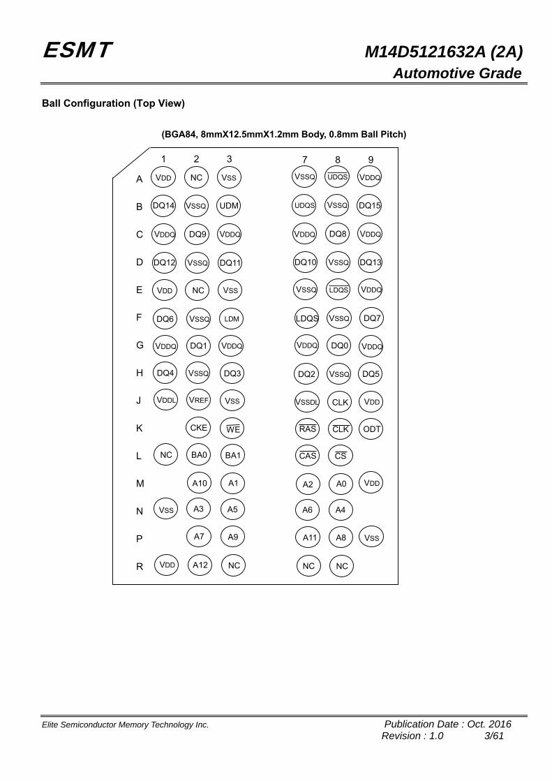
Elite Semiconductor Memory Technology Inc. Publication Date : Oct. 2016 Revision : 1.0 3/61
Ball Configuration (Top View)
(BGA84, 8mmX12.5mmX1.2mm Body, 0.8mm Ball Pitch)
VDD
DQ14
DQ12
DQ6
A
B
C
D
E
F
G
H
J
K
L
M
N
P
R
NC
VSSQ
VDDQ
VSSQ
VSSQ
DQ1
CKE
BA0
A10
VSS
UDM
DQ11
VDDQ
DQ15
DQ13
VSSQ
DQ10
LDQS
DQ2
UDQS
VSSQ
VDDQ
VSSQ
CLK
1 2 3 7 8 9
A3
A7
A12
DQ4
NC
DQ9
VDD
VDDQ
VDDL
VSS
VDD
NC
VSSQ
VREF
VDDQ
VSS
LDM
VDDQ
BA1
A1
A5
A9
NC
DQ3
VSS
WE
UDQS
DQ8 VDDQ
RAS
CAS
A2
A6
A11
NC
CS
A0
A4
A8
NC
CLK
VSSQ LDQS VDDQ
DQ7
DQ5
VDD
VDDQ
VDD
VSS
VDDQDQ0
VSSQ
VSSDL
ODT
VSSQ

ESMT M14D5121632A (2A) Automotive Grade
Elite Semiconductor Memory Technology Inc. Publication Date : Oct. 2016 Revision : 1.0 4/61
Pin Description
Pin Name Function Pin Name Function
A0~A12, BA0,BA1
Address inputs - Row address A0~A12 - Column address A0~A9 A10/AP : Auto Precharge BA0, BA1 : Bank selects (4 Banks)
DM (LDM, UDM)
DM is an input mask signal for write data. LDM is DM for DQ0~DQ7 and UDM is DM for DQ8~DQ15.
DQ0~DQ15 Data-in/Data-out CLK, CLK Differential clock input
RAS Command input CKE Clock enable
CAS Command input CS Chip select
WE Command input VDDQ Supply Voltage for DQ
VSS Ground VSSQ Ground for DQ
VDD Power VREF Reference Voltage
DQS, DQS
(LDQS, LDQS
UDQS, UDQS )
Bi-directional differential Data Strobe. LDQS and LDQS are DQS for DQ0~DQ7; UDQS and LDQS are DQS for DQ8~DQ15.
VDDL Supply Voltage for DLL
ODT On-Die-Termination. ODT is only applied to DQ0~DQ15, DM, DQS and DQS .
VSSDL Ground for DLL
NC No connection
Absolute Maximum Rating
Parameter Symbol Value Unit
Voltage on any pin relative to VSS VIN, VOUT -0.5 ~ 2.3 V
Voltage on VDD supply relative to VSS VDD -1.0 ~ 2.3 V
Voltage on VDDL supply relative to VSS VDDL -0.5 ~ 2.3 V
Voltage on VDDQ supply relative to VSS VDDQ -0.5 ~ 2.3 V
Storage temperature TSTG -55 ~ +100 C° ( Note *)
Stresses greater than those listed under “Absolute Maximum Ratings” may cause permanent damage to the device. This is a stress rating only and functional operation of the device at these or any other conditions above those indicated in the operational sections of this specification is not implied. Exposure to absolute maximum rating conditions for extended periods may affect reliability. Note *: Storage Temperature is the case surface temperature on the center/top side of the DRAM.

ESMT M14D5121632A (2A) Automotive Grade
Elite Semiconductor Memory Technology Inc. Publication Date : Oct. 2016 Revision : 1.0 5/61
Operation Temperature Condition Parameter Symbol Value Unit
Operation temperature TC (V grade) -40~+95 C°
TC (VA grade) -40~+105 C°
Note: 1. Operating temperature is the case surface temperature on the center/top side of the DRAM. 2. Supporting -40 to +85 with full AC and DC specifications. Supporting -40 to + 85 and being able to extend to + 95 for V grade with doubling auto-refresh commands in
frequency to a 32ms period ( tREFI = 3.9μs ) and higher temperature Self-Refresh entry via A7 “1” on EMRS(2); extend to +105 C° for VA grade with quadrupling auto-refresh commands in frequency to a 16ms period ( tREFI = 1.95μs ). If TC
> +95 C° , the device can’t support Self refresh function. 3. ODT resistance, the input/ output impedance, and IDD values must be derated when TC < 0 C° or > +85 C° .
DC Operation Condition & Specifications
DC Operation Condition (Recommended DC operating conditions)
Parameter Symbol Min. Typ. Max. Unit Note
Supply voltage VDD 1.7 1.8 1.9 V 4,9
Supply voltage for DLL VDDL 1.7 1.8 1.9 V 4,9
Supply voltage for output VDDQ 1.7 1.8 1.9 V 4,9
Input reference voltage VREF 0.49 x VDDQ 0.5 x VDDQ 0.51 x VDDQ V 1,2,9
Termination voltage (system) VTT VREF - 0.04 VREF VREF + 0.04 V 3,9
Input logic high voltage VIH (DC) VREF + 0.125 - VDDQ + 0.3 V
Input logic low voltage VIL (DC) -0.3 - VREF - 0.125 V
(All voltages referenced to VSS)
Parameter Symbol Value Unit Note
Minimum required output pull-up under AC test load VOH VTT + 0.603 V 8
Maximum required output pull-down under AC test load VOL VTT - 0.603 V 8
Input leakage current |I LI| 5 uA 5
Output leakage current |I LO| 5 uA 6
Output minimum source DC current ( VDDQ(min); VOUT =1.42V )
I OH -13.4 mA 7, 8
Output minimum sink DC current ( VDDQ(min); VOUT = 0.28V )
I OL +13.4 mA 7, 8
Note: 1. The value of VREF may be selected by the user to provide optimum noise margin in the system. Typically the value of VREF is expected to be about 0.5 x VDDQ of the transmitting device and VREF is expected to track variations in VDDQ. 2. Peak to peak AC noise on VREF may not exceed ±2% VREF(DC). 3. VTT of transmitting device must track VREF of receiving device. 4. VDDQ and VDDL track VDD. AC parameters are measured with VDD, VDDQ and VDDL tied together.
5. Any input 0V ≤ VIN ≤ VDD; all other balls not under test = 0V. 6. 0V ≤ VOUT ≤ VDDQ; DQ and ODT disabled. 7. The DC value of VREF applied to the receiving device is expected to be set to VTT. 8. After OCD calibration to 18Ω at TC = 25, VDD = VDDQ = 1.8V 9. There is no specific device VDD supply voltage requirement for SSTL_18 compliance. However, under all conditions VDDQ must be less than or equal to VDD.

ESMT M14D5121632A (2A) Automotive Grade
Elite Semiconductor Memory Technology Inc. Publication Date : Oct. 2016 Revision : 1.0 6/61
DC Specifications (IDD values are for the operation range of Voltage and Temperature)
Parameter Symbol Test Condition Version
Unit-1.8 -2.5
Operating Current (Active - Precharge) IDD0
One bank; tCK = tCK (IDD), tRC = tRC (IDD), tRAS = tRAS (IDD)min; CKE is High, CS is HIGH between valid commands; Address bus inputs are SWITCHING; Data bus inputs are SWITCHING
80 75 mA
Operating Current (Active - Read - Precharge)
IDD1
One bank; IOUT = 0mA; BL = 4, CL = CL(IDD), AL = 0; tCK = tCK (IDD), tRC = tRC (IDD), tRAS = tRAS (IDD)min, tRCD = tRCD (IDD); CKE is HIGH, CS is HIGH between valid commands; Address bus inputs are SWITCHING; Data pattern is same as IDD4W
100 95 mA
Precharge Power-Down Standby Current
IDD2P
All banks idle; tCK = tCK (IDD); CKE is LOW; Other control and address bus inputs are STABLE; Data bus inputs are FLOATING
12 12 mA
Precharge Quiet Standby Current IDD2Q
All banks idle; tCK = tCK (IDD); CKE is HIGH, CS is HIGH; Other control and address bus inputs are STABLE; Data bus inputs are FLOATING
40 40 mA
Idle Standby Current IDD2N
All banks idle; tCK = tCK (IDD); CKE is HIGH, CS is HIGH; Other control and address bus inputs are SWITCHING;Data bus inputs are SWITCHING
45 45 mA
Active Power-down Standby Current IDD3P
All banks open; tCK = tCK (IDD); CKE is LOW; Other control and address bus inputs are STABLE; Data bus input are FLOATING
Fast PDN Exit MRS(12) = 0
35 35
mA Slow PDN Exit MRS(12) = 1
20 20
Active Standby Current IDD3N
All banks open; tCK = tCK (IDD), tRAS = tRAS (IDD)max, tRP = tRP (IDD); CKE is HIGH, CS is HIGH between valid commands; Other control and address bus inputs are SWITCHING;Data bus inputs are SWITCHING
50 50 mA
Operation Current (Read) IDD4R
All banks open, continuous burst Reads, IOUT = 0mA; BL = 4, CL = CL (IDD), AL = 0; tCK = tCK (IDD), tRAS = tRAS (IDD)max, tRP = tRP (IDD); CKE is HIGH, CS is HIGH between valid commands; Address bus inputs are SWITCHING; Data pattern is the same as IDD4W;
160 140 mA
Operation Current (Write) IDD4W
All banks open, continuous burst Writes; BL = 4, CL = CL (IDD), AL = 0; tCK = tCK (IDD), tRAS = tRAS (IDD)max, tRP = tRP (IDD); CKE is HIGH, CS is HIGH between valid commands; Address bus inputs are SWITCHING; Data bus inputs are SWITCHING
150 130 mA

ESMT M14D5121632A (2A) Automotive Grade
Elite Semiconductor Memory Technology Inc. Publication Date : Oct. 2016 Revision : 1.0 7/61
Parameter Symbol Test Condition Version
Unit-1.8 -2.5
Auto Refresh Current IDD5
tCK = tCK (IDD); Refresh command every tRFC (IDD) interval; CKE is HIGH, CS is HIGH between valid commands;Other control and address bus inputs are SWITCHING;Data bus inputs are SWITCHING
100 100 mA
Self Refresh Current IDD6
Self Refresh Mode; CLK and CLK at 0V; CKE≤ 0.2V; Other control and address bus inputs are FLOATING;Data bus inputs are FLOATING
8 mA
Operating Current (Bank interleaving) IDD7
All bank interleaving Reads, IOUT = 0mA; BL = 4, CL= CL (IDD), AL = tRCD (IDD) – 1 × tCK (IDD);tCK = tCK (IDD), tRC = tRC (IDD), tRRD = tRRD (IDD), tRCD = 1 × tCK (IDD); CKE is HIGH, CS is HIGH between valid commands;Address bus inputs are STABLE during Deslects; Data pattern is the same as IDD4W;
210 200 mA
Note: 1. IDD specifications are tested after the device is properly initialized. 2. Input slew rate is specified by AC Input Test Condition. 3. IDD parameters are specified with ODT disabled. 4. Data bus consists of DQ, DM, DQS and DQS , IDD values must be met with all combinations of EMRS bits 10 and 11. 5. Definitions for IDD: LOW is defined as VIN ≤ VIL (AC) (max.).
HIGH is defined as VIN VIH (AC) (min.). STABLE is defined as inputs stable at a HIGH or LOW level.
FLOATING is defined as inputs at VREF = VDDQ/2 SWITCHING is defined as: Address and control signal Inputs are changed between HIGH and LOW every other clock cycle (once per two clocks), and DQ (not including mask or strobe) signal inputs are changed between HIGH and LOW every other data transfer (once per clock). 6. When TC ≧ +85 , IDD6 must be derated by 80%. IDD6 will increase by this amount if TC ≧ +85 and double refresh option is still enabled. 7. AC Timing for IDD test conditions For purposes of IDD testing, the following parameters are to be utilized.
Parameter -1.8 -2.5
Unit DDR2-1066 (7-7-7)
DDR2-800 (5-5-5)
CL (IDD) 7 5 tCK tRCD (IDD) 13.125 12.5 ns tRC (IDD) 58.125 57.5 ns tRRD (IDD) 10 10 ns tCK (IDD) 1.875 2.5 ns tRAS (IDD) min. 45 45 ns tRAS (IDD) max. 70000 ns tRP (IDD) 13.25 12.5 ns tRFC (IDD) 105 105 ns

ESMT M14D5121632A (2A) Automotive Grade
Elite Semiconductor Memory Technology Inc. Publication Date : Oct. 2016 Revision : 1.0 8/61
AC Operation Conditions & Timing Specification
AC Operation Conditions
Parameter Symbol 1.8 -2.5
Unit NoteMin. Max. Min. Max.
Input High (Logic 1) Voltage VIH(AC) VREF + 0.2 VREF + 0.2 V
Input Low (Logic 0) Voltage VIL(AC) VREF - 0.2 VREF - 0.2 V
Input Differential Voltage VID(AC) 0.5 VDDQ+0.6 0.5 VDDQ+0.6 V 1
Input Crossing Point Voltage VIX(AC) 0.5 x VDDQ - 0.175
0.5 x VDDQ + 0.175
0.5 x VDDQ - 0.175
0.5 x VDDQ + 0.175
V 2
Output Crossing Point Voltage VOX(AC) 0.5 x VDDQ - 0.125
0.5 x VDDQ + 0.125
0.5 x VDDQ - 0.125
0.5 x VDDQ + 0.125
V 2
Note: 1. VID(AC) specifies the input differential voltage |VTR – VCP| required for switching, where VTR is the true input signal (such as CLK,DQS) and VCP is the complementary input signal (such as CLK , DQS ). The minimum value is equal to VIH(AC) – VIL(AC). 2. The typical value of VIX / VOX(AC) is expected to be about 0.5 x VDDQ of the transmitting device and VIX / VOX(AC) is
expected to track variations in VDDQ. VIX / VOX(AC) indicates the voltage at which differential input / output signals must cross.
Input / Output Capacitance
Parameter Symbol Min. Max. Unit Note
Input capacitance (A0~A12, BA0~BA1, CKE, CS , RAS , CAS , WE , ODT)
CIN1 1 2 pF 1
Input capacitance (CLK, CLK ) CIN2 1 2 pF 1
DQS, DQS & Data input/output capacitance CI / O 2.5 4 pF 2
Input capacitance (DM) CIN3 2.5 4 pF 2
Note: 1. Capacitance delta is 0.25 pF. 2. Capacitance delta is 0.5 pF.

ESMT M14D5121632A (2A) Automotive Grade
Elite Semiconductor Memory Technology Inc. Publication Date : Oct. 2016 Revision : 1.0 9/61
AC Overshoot / Undershoot Specification
Parameter Pin Value
Unit1.8 -2.5
Maximum peak amplitude allowed for overshoot
Address, CKE, CS , RAS , CAS , WE ,
ODT, CLK, CLK , DQ, DQS, DQS , DM0.5 0.5 V
Maximum peak amplitude allowed for undershoot
Address, CKE, CS , RAS , CAS , WE ,
ODT, CLK, CLK , DQ, DQS, DQS , DM0.5 0.5 V
Maximum overshoot area above VDD Address, CKE, CS , RAS , CAS , WE ,
ODT, 0.5 0.66 V-ns
CLK, CLK , DQ, DQS, DQS , DM 0.19 0.23 V-ns
Maximum undershoot area below VSS Address, CKE, CS , RAS , CAS , WE ,
ODT, 0.5 0.66 V-ns
CLK, CLK , DQ, DQS, DQS , DM 0.19 0.23 V-ns

ESMT M14D5121632A (2A) Automotive Grade
Elite Semiconductor Memory Technology Inc. Publication Date : Oct. 2016 Revision : 1.0 10/61
AC Operating Test Conditions
Parameter Value Unit Note
Input reference voltage ( VREF ) 0.5 x VDDQ V 1
Input signal maximum peak swing ( VSWING(max.) ) 1.0 V 1
Input signal minimum slew rate 1.0 V/ns 2,3
Input level VIH / VIL V
Input timing measurement reference level VREF V
Output timing measurement reference level (VOTR) 0.5 x VDDQ V 4
Note: 1. Input waveform timing is referenced to the input signal crossing through the VIH / VIL (AC) level applied to the device under
test. 2. The input signal minimum slew rate is to be maintained over the range from VREF to VIH (AC) (min.) for rising edges and the
range from VREF to VIL (AC)(max.) for falling edges as shown in the below figure. 3. AC timings are referenced with input waveforms switching from VIL (AC) to VIH (AC) on the positive transitions and VIH (AC) to
VIL (AC) on the negative transitions. 4. The VDDQ of the device under test is reference.

ESMT M14D5121632A (2A) Automotive Grade
Elite Semiconductor Memory Technology Inc. Publication Date : Oct. 2016 Revision : 1.0 11/61
AC Timing Parameter & Specifications
Parameter Symbol -1.8 -2.5
Unit NoteMin. Max. Min. Max.
Clock period
CL=7
tCK (avg)
1875 7500 - -
ps 13
CL=6 X X 2500 8000
CL=5 X X 2500 8000
CL=4 X X 3750 8000
CL=3 X X 5000 8000
DQ output access time from CLK/ CLK
tAC -350 +350 -400 +400 ps 10
CLK high-level width tCH (avg) 0.48 0.52 0.48 0.52 tCK (avg) 13
CLK low-level width tCL (avg) 0.48 0.52 0.48 0.52 tCK (avg) 13
DQS output access time from CLK/ CLK
tDQSCK -300 +300 -350 +350 ps 10
Clock to first rising edge of DQS delay tDQSS -0.25 +0.25 -0.25 +0.25 tCK (avg)
Data-in and DM setup time (to DQS)
tDS (base) 0 50 ps 4
Data-in and DM hold time (to DQS)
tDH (base) 75 125 ps 5
DQ and DM input pulse width (for each input) tDIPW 0.35 0.35 tCK (avg)
Address and Control Input setup time tIS (base) 125 175 ps 4
Address and Control Input hold time tIH (base) 200 250 ps 5
Control and Address input pulse width tIPW 0.6 0.6 tCK (avg)
DQS input high pulse width tDQSH 0.35 0.35 tCK (avg)
DQS input low pulse width tDQSL 0.35 0.35 tCK (avg)
DQS falling edge to CLK rising setup time tDSS 0.2 0.2 tCK (avg)
DQS falling edge from CLK rising hold time tDSH 0.2 0.2 tCK (avg)
Data strobe edge to output data edge tDQSQ 175 200 ps
Data-out high-impedance window from CLK/ CLK
tHZ tAC(max.) tAC(max.) ps 10
Data-out low-impedance window from CLK/ CLK
tLZ
(DQS) tAC(min.) tAC(max.) tAC(min.) tAC(max.) ps 10
DQ low-impedance window from CLK/ CLK
tLZ
(DQ) 2 x tAC(min.) tAC(max.) 2 x tAC(min.) tAC(max.) ps 10
Half clock period tHP Min
(tCL(abs),tCH(abs))
Min
(tCL(abs),tCH(abs))
ps 6,13
ESMT M14D5121632A (2A) Automotive Grade
Elite Semiconductor Memory Technology Inc. Publication Date : Oct. 2016 Revision : 1.0 12/61
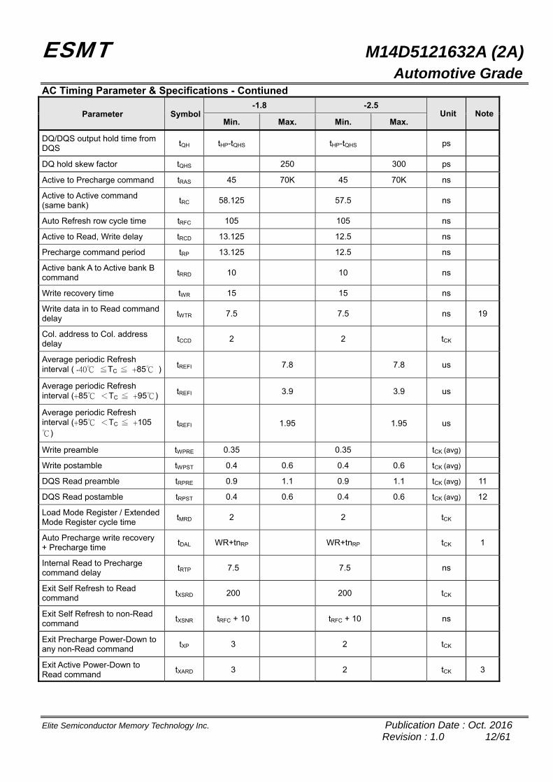
AC Timing Parameter & Specifications - Contiuned
Parameter Symbol -1.8 -2.5
Unit NoteMin. Max. Min. Max.
DQ/DQS output hold time from DQS tQH tHP-tQHS tHP-tQHS ps
DQ hold skew factor tQHS 250 300 ps
Active to Precharge command tRAS 45 70K 45 70K ns
Active to Active command (same bank) tRC 58.125 57.5 ns
Auto Refresh row cycle time tRFC 105 105 ns
Active to Read, Write delay tRCD 13.125 12.5 ns
Precharge command period tRP 13.125 12.5 ns
Active bank A to Active bank B command tRRD 10 10 ns
Write recovery time tWR 15 15 ns
Write data in to Read command delay tWTR 7.5 7.5 ns 19
Col. address to Col. address delay tCCD 2 2 tCK
Average periodic Refresh interval ( -40 ≦TC ≦ +85 ) tREFI 7.8 7.8 us
Average periodic Refresh interval (+85 <TC ≦ +95) tREFI 3.9 3.9 us
Average periodic Refresh interval (+95 <TC ≦ +105)
tREFI 1.95 1.95 us
Write preamble tWPRE 0.35 0.35 tCK (avg)
Write postamble tWPST 0.4 0.6 0.4 0.6 tCK (avg)
DQS Read preamble tRPRE 0.9 1.1 0.9 1.1 tCK (avg) 11
DQS Read postamble tRPST 0.4 0.6 0.4 0.6 tCK (avg) 12
Load Mode Register / Extended Mode Register cycle time tMRD 2 2 tCK
Auto Precharge write recovery + Precharge time tDAL WR+tnRP WR+tnRP tCK 1
Internal Read to Precharge command delay tRTP 7.5 7.5 ns
Exit Self Refresh to Read command tXSRD 200 200 tCK
Exit Self Refresh to non-Read command tXSNR tRFC + 10 tRFC + 10 ns
Exit Precharge Power-Down to any non-Read command tXP 3
2 tCK
Exit Active Power-Down to Read command tXARD 3
2 tCK 3

ESMT M14D5121632A (2A) Automotive Grade
Elite Semiconductor Memory Technology Inc. Publication Date : Oct. 2016 Revision : 1.0 13/61
AC Timing Parameter & Specifications - Contiuned
Parameter Symbol -1.8 -2.5
Unit NoteMin. Max. Min. Max.
Exit active power-down to Read command (slow exit / low power mode)
tXARDS 10 - AL
8 - AL tCK 2,3
CKE minimum pulse width (high and low pulse width) tCKE 3
3 tCK
Minimum time clocks remains ON after CKE asynchronously drops low
tDELAY tIS + tCK (avg)+tIH tIS + tCK
(avg)+tIH ns
Output impedance test driver delay tOIT 0 12 0 12 ns
MRS command to ODT update delay tMOD 0 12 0 12 ns
ODT turn-on delay tAOND 2 2 2 2 tCK
ODT turn-on tAON tAC(min.) tAC(max.) + 2575 tAC(min.) tAC(max.) +
700 ps 14,16
ODT turn-on (Power-Down mode) tAONPD tAC(min.) +
2000
3 x tCK +tAC(max.) +
1000
tAC(min.) + 2000
2 x tCK +tAC(max.) +
1000 ps
ODT turn-off delay tAOFD 2.5 2.5 2.5 2.5 tCK 15,17,18
ODT turn-off tAOF tAC(min.) tAC(max.) + 600 tAC(min.) tAC(max.) +
600 ps
ODT turn-off (Power-Down mode) tAOFPD tAC(min.) +
2000
2.5 x tCK +tAC(max.) +
1000
tAC(min.) + 2000
2.5 x tCK +tAC(max.) +
1000 ps
ODT to Power-Down entry latency tANPD 4 3 tCK
ODT Power-Down exit latency tAXPD 11 8 tCK Note: 1. tDAL[nCLK] = WR[nCLK] + tnRP [nCLK] =WR+RUtRP[ps]/tCK(avg)[ps], where WR is the value programmed in the mode
register set and RU status for round up. 2. AL: Additive Latency. 3. MRS A12 bit defines which Active Power-Down Exit timing to be applied. 4. The figures of Input Waveform Timing 1 and 2 are referenced from the input signal crossing at the VIH (AC) level for a rising
signal and VIL (AC) for a falling signal applied to the device under test. 5. The figures of Input Waveform Timing 1 and 2 are referenced from the input signal crossing at the VIL (DC) level for a rising
signal and VIH (DC) for a falling signal applied to the device under test.

ESMT M14D5121632A (2A) Automotive Grade
Elite Semiconductor Memory Technology Inc. Publication Date : Oct. 2016 Revision : 1.0 14/61
6. tHP is the minimum of the absolute half period of the actual input clock. tHP is an input parameter but not an input
specification parameter. It is used in conjunction with tQHS to derive the DRAM output timing tQH. The value to be used for tQH calculation is determined by the following equation;
tHP = Min ( tCH (abs), tCL (abs) ), where: tCH (abs) is the minimum of the actual instantaneous clock HIGH time; tCL (abs) is the minimum of the actual instantaneous clock LOW time; 7. tQHS accounts for:
a. The pulse duration distortion of on-chip clock circuits, which represents how well the actual tHP at the input is transferred to the output; and
b. The worst case push-out of DQS on one transition followed by the worst case pull-in of DQ on the next transition, both of which are independent of each other, due to data pin skew, output pattern effects, and p-channel to n-channel variation of the output drivers.
8. tQH = tHP - tQHS, where: tHP is the minimum of the absolute half period of the actual input clock; and tQHS is the specification value under the max column. The less half-pulse width distortion present, the larger the tQH value is; and the larger the valid data eye will be.
Examples: a. If the system provides tHP of 825 ps into a DDR2-1066 SDRAM, the DRAM provides tQH of 575 ps minimum. b. If the system provides tHP of 900 ps into a DDR2-1066 SDRAM, the DRAM provides tQH of 650 ps minimum.
9. RU stands for round up. WR refers to the tWR parameter stored in the MRS. 10. When the device is operated with input clock jitter, this parameter needs to be de-rated by the actual tERR (6-10per) of the
input clock. (output de-ratings are relative to the SDRAM input clock.) For example, if the measured jitter into a DDR2- 1066 SDRAM has tERR (6-10per)(min.) = - 202 ps and tERR (6-10per)(max.) = + 223 ps, then tDQSCK (min.)(derated) = tDQSCK (min.) - tERR (6-10per)(max.) = -300 ps – 223 ps = -523 ps and tDQSCK (max.) (derated) = tDQSCK (max.) - tERR (6-10per)(min.) = 300 ps + 202 ps = +502 ps. Similarly, tLZ (DQ) for DDR2-1066 de-rates to tLZ (DQ)(min.)(derated) = -700 ps - 223 ps = -923 ps and tLZ (DQ)(max.)(derated) = 350 ps + 202 ps = +552 ps.
11. When the device is operated with input clock jitter, this parameter needs to be de-rated by the actual tJIT (per) of the input clock. (output de-ratings are relative to the SDRAM input clock.) For example, if the measured jitter into a DDR2-1066 SDRAM has tJIT (per)(min.) = - 72 ps and tJIT (per)(max.) = + 63 ps, then tRPRE (min.)(derated) = tRPRE (min.) + tJIT (per)(min.) = 0.9 x tCK (avg) - 72 ps = + 1615.5 ps and tRPRE (max.)(derated) = tRPRE (max.) + tJIT (per)(max.) = 1.1 x tCK (avg) + 63 ps = + 2125.5 ps.
12. When the device is operated with input clock jitter, this parameter needs to be de-rated by the actual tJIT (duty) of the input clock. (output de-ratings are relative to the SDRAM input clock.) For example, if the measured jitter into a DDR2-1066 SDRAM has tJIT (duty)(min.) = - 72 ps and tJIT (duty)(max.) = + 63 ps, then tRPST (min.)(derated) = tRPST (min.) + tJIT (duty)(min.) = 0.4 x tCK (avg) - 72 ps = + 678 ps and tRPST (max.)(derated) = tRPST (max.) + tJIT (duty)(max.) = 0.6 x tCK (avg) + 63 ps = + 1188 ps.
13. Refer to the Clock Jitter table. 14. ODT turn on time min is when the device leaves high impedance and ODT resistance begins to turn on. ODT turn on time max is when the ODT resistance is fully on. Both are measured from tAOND. 15. ODT turn off time min is when the device starts to turn off ODT resistance. ODT turn off time max is when the bus is in high impedance. Both are measured from tAOFD. 16. When the device is operated with input clock jitter, this parameter needs to be de-rated by the actual tERR (6-10per) of the
input clock. (output de-ratings are relative to the SDRAM input clock.) 17. When the device is operated with input clock jitter, this parameter needs to be derated by - tJIT (duty)(max.) - tERR
(6-10per)(max.) and - tJIT (duty)(min.) - tERR (6-10per)(min.) of the actual input clock. (output deratings are relative to the SDRAM input clock.) For example, if the measured jitter into a DDR2- 1066 SDRAM has tERR (6-10per)(min.) = - 202 ps, tERR (6- 10per)(max.) = + 223 ps, tJIT (duty)(min.) = - 66 ps and tJIT (duty)(max.) = + 74 ps, then tAOF(min.)(derated) = tAOF(min.) + - tJIT (duty)(max.) -

ESMT M14D5121632A (2A) Automotive Grade
Elite Semiconductor Memory Technology Inc. Publication Date : Oct. 2016 Revision : 1.0 15/61
tERR (6-10per)(max.) = - 350 ps + - 74 ps - 223 ps = - 647 ps and tAOF(max.)(derated) = tAOF(max.) + - tJIT (duty)(min.) - tERR (6-10per)(min.) = 950 ps + 66 ps + 202 ps = + 1218 ps.
18. For tAOFD of DDR2-800/1066, the 1/2 clock of tCK in the 2.5 x tCK assumes a tCH (avg), average input clock HIGH pulse width of 0.5 relative to tCK (avg). tAOF (min.) and tAOF (max.) should each be derated by the same amount as the actual amount of tCH (avg) offset present at the DRAM input with respect to 0.5. For example, if an input clock has a worst case tCH (avg) of 0.48, the tAOF (min.) should be derated by subtracting 0.02 x tCK (avg) from it, whereas if an input clock has a worst case tCH (avg) of 0.52, the tAOF (max.) should be derated by adding 0.02 x tCK (avg) to it. Therefore, we have; tAOF (min.)(derated) = tAC (min.) - [0.5 - Min(0.5, tCH (avg)(min.))] x tCK (avg) tAOF (max.)(derated) = tAC (max.) + 0.6 + [Max(0.5, tCH (avg)(max.)) - 0.5] x tCK (avg) or tAOF (min.)(derated) = Min(tAC (min.), tAC (min.) - [0.5 - tCH (avg)(min.)] x tCK (avg)) tAOF (max.)(derated) = 0.6 + Max(tAC (max.), tAC (max.) + [tCH (avg)(max.) - 0.5] x tCK (avg)), where: tCH (avg)(min.) and tCH (avg)(max.) are the minimum and maximum of tCH (avg) actually measured at the DRAM input balls.
19. tWTR is at lease two clocks (2 x tCK or 2 x nCK) independent of operation frequency. 20. If tCK < 1.875ns, the device can not support Write with Auto Precharge function.

ESMT M14D5121632A (2A) Automotive Grade
Elite Semiconductor Memory Technology Inc. Publication Date : Oct. 2016 Revision : 1.0 16/61
ODT DC Electrical Characteristics
Parameter Symbol Min. Typ. Max. Unit
Rtt effective impedance value for 75Ω setting EMRS(1) [A6, A2] = 0, 1 Rtt1(eff) 60 75 90 Ω
Rtt effective impedance value for 150Ω setting EMRS(1) [A6, A2) = 1, 0 Rtt2(eff) 120 150 180 Ω
Rtt effective impedance value for 50Ω setting EMRS(1) [A6, A2] = 1, 1 Rtt3(eff) 40 50 60 Ω
Deviation of VM with respect to VDDQ /2 VM -6 - +6 %
Note: Measurement Definition for Rtt(eff) :
Rtt(eff) is determined by separately applying VIH(AC) and VIL(AC) to test pin, and then measuring current I(VIH(AC)) and I(VIL(AC)) respectively.
Measurement Definition for VM : Measure voltage (VM) at test pin with no load.
OCD Default Characteristics
Parameter Min. Typ. Max. Unit Note
Output impedance 12.6 18 23.4 Ω 1
Pull-up and pull-down mismatch 0 - 4 Ω 1,2,3
Output slew rate 1.5 - 5 V/ns 1,4,5
Note: 1. Absolute specifications: the operation range of Voltage and Temperature. 2. Impedance measurement condition for output source DC current: VDDQ = 1.7V; VOUT = 1,420mV; (VOUT - VDDQ)/IOH must be
less than 23.4Ω for values of VOUT between VDDQ and VDDQ - 280mV. Impedance measurement condition for output sink DC current: VDDQ = 1.7V; VOUT = 280mV; VOUT/IOL must be less than 23.4Ω for values of VOUT between 0V and 280mV.
3. Mismatch is absolute value between pull-up and pull-down; both are measured at same temperature and voltage. 4. Slew rate measured from VIL (AC) to VIH (AC). 5. The absolute value of the slew rate as measured from DC to DC is equal to or greater than the slew rate as measured from
AC to AC.

ESMT M14D5121632A (2A) Automotive Grade
Elite Semiconductor Memory Technology Inc. Publication Date : Oct. 2016 Revision : 1.0 17/61
Clock Jitter [ DDR2- 1066, 800 ]
Parameter Symbol -1.8 -2.5
Unit Note Min. Max. Min. Max.
Average clock period tCK (avg) 1875 7500 2500 8000 ps 1 Clock period jitter tJIT (per) -90 90 -100 100 ps 5 Clock period jitter during DLL locking period
tJIT (per,lck) -80 80 -80 80 ps 5
Cycle to cycle period jitter tJIT (cc) -180 180 -200 200 ps 6 Cycle to cycle clock period jitter During DLL locking period
tJIT (cc, lck) -160 160 -160 160 ps 6
Cumulative error across 2 cycles
tERR (2per) -132 132 -150 150 ps 7
Cumulative error across 3 cycles
tERR (3per) -157 157 -175 175 ps 7
Cumulative error across 4 cycles
tERR (4per) -175 175 -200 200 ps 7
Cumulative error across 5 cycles
tERR (5per) -188 188 -200 200 ps 7
Cumulative error across n=6,7,8,9,10 cycles
tERR (6-10per)
-250 250 -300 300 ps 7
Cumulative error across n=11,12,….49,50 cycles
tERR (11-50per)
-425 425 -450 450 ps 7
Average high pulse width tCH (avg) 0.48 0.52 0.48 0.52
tCK
(avg)2
Average low pulse width tCL (avg) 0.48 0.52 0.48 0.52
tCK
(avg)3
Duty cycle jitter tJIT (duty) -75 75 -100 100 ps 4 Note: 1. tCK (avg) is calculated as the average clock period across any consecutive 200 cycle window.
2. tCH (avg) is defined as the average HIGH pulse width, as calculated across any consecutive 200 HIGH pulses.
3. tCL (avg) is defined as the average LOW pulse width, as calculated across any consecutive 200 LOW pulses.
4. tJIT (duty) is defined as the cumulative set of tCH jitter and tCL jitter. tCH jitter is the largest deviation of any single tCH from tCH
(avg). tCL jitter is the largest deviation of any single tCL from tCL (avg). tJIT (duty) is not subject to production test. tJIT (duty) = Min./Max. of tJIT (CH), tJIT (CL), where: tJIT (CH) = tCH j - tCH (avg) where j =1 to 200 tJIT (CL) = tCL j - tCL (avg) where j =1 to 200
ESMT M14D5121632A (2A) Automotive Grade
Elite Semiconductor Memory Technology Inc. Publication Date : Oct. 2016 Revision : 1.0 18/61
5. tJIT (per) is defined as the largest deviation of any single tCK from tCK (avg).
tJIT (per) = Min./Max. of tCK j - tCK (avg) where j =1 to 200 tJIT (per) defines the single period jitter when the DLL is already locked. tJIT (per, lck) uses the same definition for single period jitter, during the DLL locking period only. tJIT (per) and tJIT (per, lck) are not subject to production testing.
6. tJIT (cc) is defined as the difference in clock period between two consecutive clock cycles : tJIT (cc) = Max. of | tCK i +1 - tCK i| tJIT (cc) defines the cycle to cycle jitter when the DLL is already locked. tJIT (cc, lck) uses the same definition for cycle to cycle jitter, during the DLL locking period only. tJIT (cc) and tJIT (cc, lck) are not subject to production testing.
7. tERR (nper) is defined as the cumulative error across multiple consecutive cycles from tCK (avg).
tERR (nper) is not subject to production testing.
8. These parameters are specified per their average values, however it is understood that the following relationship between
the average timing and the absolute instantaneous timing holds at all times. (Min. and max. of SPEC values are to be used for calculations in the table below.)
Parameter Symbol Min. Max. Unit
Absolute clock period tCK (abs) tCK (avg)(min.) + tJIT (per)(min.) tCK (avg)(max.) + tJIT (per)(max.) psAbsolute clock high pulse width
tCH (abs) tCH (avg)(min.) x tCK (avg)(min.) +
tJIT (duty)(min.) tCH (avg)(max.) x tCK (avg)(max.)
+ tJIT (duty)(max.) ps
Absolute clock low pulse width tCL (abs)
tCL (avg)(min.) x tCK (avg)(min.) + tJIT (duty)(min.)
tCL (avg)(max.) x tCK (avg)(max.) + tJIT (duty)(max.)
ps
Example: For DDR2-1066, tCH (abs)(min.) = (0.48 x 1875ps) - 75 ps = 825 ps
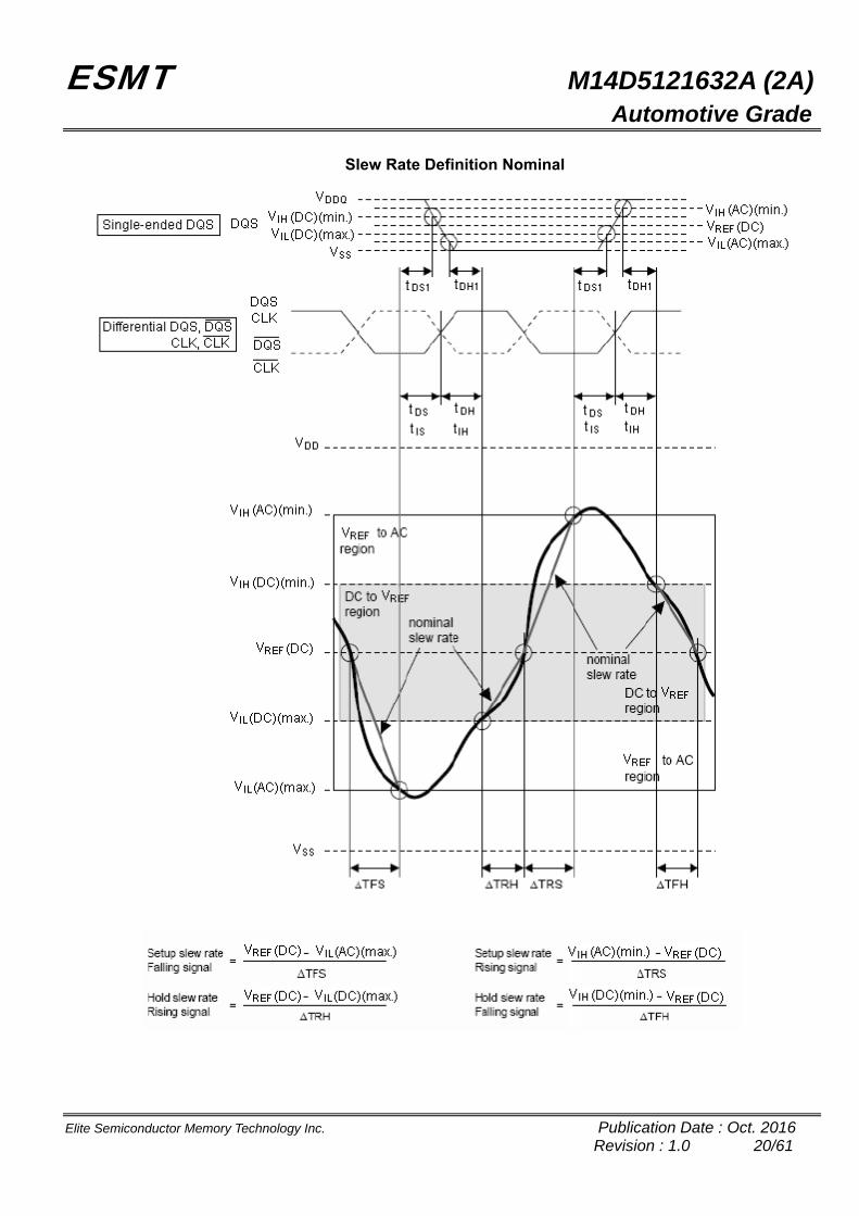
Input Slew Rate De-rating
For all input signals the total tIS, tDS (setup time) and tIH, tDH (hold time) required is calculated by adding the data sheet tIS (base), tDS (base) and tIH (base), tDH (base) value to the ΔtIS, ΔtDS and ΔtIH, ΔtDH de-rating value respectively. Example: tDS (total setup time) = tDS (base) + ΔtDS. Setup (tIS, tDS) nominal slew rate for a rising signal is defined as the slew rate between the last crossing of VREF (DC) and the first crossing of VIH (AC)(min.). Setup (tIS, tDS) nominal slew rate for a falling signal is defined as the slew rate between the last crossing of VREF (DC) and the first crossing of VIL (AC)(max.). If the actual signal is always earlier than the nominal slew rate line between shaded ‘VREF (DC) to AC region’, use nominal slew rate for de-rating value (See the figure of Slew Rate Definition Nominal). If the actual signal is later than the nominal slew rate line anywhere between shaded ‘VREF (DC) to AC region’, the slew rate of a tangent line to the actual signal from the AC level to DC level is used for de-rating value (see the figure of Slew Rate Definition Tangent). Hold (tIH, tDH) nominal slew rate for a rising signal is defined as the slew rate between the last crossing of VIL (DC)(max.) and the first crossing of VREF (DC). Hold (tIH, tDH) nominal slew rate for a falling signal is defined as the slew rate between the last crossing of VIH (DC)(min.) and the first crossing of VREF (DC). If the actual signal is always later than the nominal slew rate line between shaded ‘DC level to VREF (DC) region’, use nominal slew rate for de-rating value (See the figure of Slew Rate Definition Nominal). If the actual signal is earlier than the nominal slew rate line anywhere between shaded ‘DC to VREF (DC) region’, the slew rate of a tangent line to the actual signal from the DC level to VREF (DC) level is used for de-rating value (see the figure of Slew Rate Definition Tangent). Although for slow slew rates the total setup time might be negative (i.e. a valid input signal will not have reached VIH / VIL (AC) at the time of the rising clock transition) a valid input signal is still required to complete the transition and reach VIH / VIL (AC). For slew rates in between the values listed in the tables below, the de-rating values may be obtained by linear interpolation. These values are typically not subject to production test. They are verified by design and characterization.

ESMT M14D5121632A (2A) Automotive Grade
Elite Semiconductor Memory Technology Inc. Publication Date : Oct. 2016 Revision : 1.0 19/61
De-rating Value of tDS/tDH with Differential DQS(DDR2-800, 1066)
DQS, DQS differential slew rate
4.0 V/ns 3.0 V/ns 2.0 V/ns 1.8 V/ns 1.6 V/ns 1.4 V/ns 1.2 V/ns 1.0 V/ns 0.8 V/ns UnitΔtDS ΔtDH ΔtDS ΔtDH ΔtDS ΔtDH ΔtDS ΔtDH ΔtDS ΔtDH ΔtDS ΔtDH ΔtDS ΔtDH ΔtDS ΔtDH ΔtDS ΔtDH
DQ
sle
w ra
te (V
/ns)
2.0 +100 +45 +100 +45 +100 +45 - - - - - - - - - - - - ps1.5 +67 +21 +67 +21 +67 +21 +79 +33 - - - - - - - - - - ps1.0 0 0 0 0 0 0 +12 +12 +24 +24 - - - - - - - - ps0.9 - - -5 -14 -5 -14 +7 -2 +19 +10 +31 +22 - - - - - - ps0.8 - - - - -13 -31 -1 -19 +11 -7 +23 +5 +35 +17 - - - - ps0.7 - - - - - - -10 -42 +2 -30 +14 -18 +26 -6 +38 +6 - - ps0.6 - - - - - - - - -10 -59 +2 -47 +14 -35 +26 -23 +38 -11 ps0.5 - - - - - - - - - - -24 -89 -12 -77 0 -65 +12 -53 ps0.4 - - - - - - - - - - - - -52 -140 -40 -128 -28 -116 ps
De-rating Value of tIS/tIH (DDR2-800, 1066)
CLK, CLK differential slew rate
2.0 V/ns 1.5 V/ns 1.0 V/ns UnitΔtIS ΔtIH ΔtIS ΔtIH ΔtIS ΔtIH
Com
man
d / A
ddre
ss s
lew
rate
(V/n
s)
4.0 +150 +94 +180 +124 +210 +154 ps 3.5 +143 +89 +173 +119 +203 +149 ps 3.0 +133 +83 +163 +113 +193 +143 ps 2.5 +120 +75 +150 +105 +180 +135 ps 2.0 +100 +45 +130 +75 +160 +105 ps 1.5 +67 +21 +97 +51 +127 +81 ps 1.0 0 0 +30 +30 +60 +60 ps 0.9 -5 -14 +25 +16 +55 +46 ps 0.8 -13 -31 +17 -1 +47 +29 ps 0.7 -22 -54 +8 -24 +38 +6 ps 0.6 -34 -83 -4 -53 +26 -23 ps 0.5 -60 -125 -30 -95 0 -65 ps 0.4 -100 -188 -70 -158 -40 -128 ps 0.3 -168 -292 -138 -262 -108 -232 ps
0.25 -200 -375 -170 -345 -140 -315 ps 0.2 -325 -500 -295 -470 -265 -440 ps
0.15 -517 -708 -487 -678 -457 -648 ps 0.1 -1000 -1125 -970 -1095 -940 -1065 ps
ESMT M14D5121632A (2A) Automotive Grade
Elite Semiconductor Memory Technology Inc. Publication Date : Oct. 2016 Revision : 1.0 20/61
Slew Rate Definition Nominal

ESMT M14D5121632A (2A) Automotive Grade
Elite Semiconductor Memory Technology Inc. Publication Date : Oct. 2016 Revision : 1.0 21/61
Slew Rate Definition Tangent

ESMT M14D5121632A (2A) Automotive Grade
Elite Semiconductor Memory Technology Inc. Publication Date : Oct. 2016 Revision : 1.0 22/61
Command Truth Table
COMMAND Note 7
CKE(n-1)Note 7
CKE(n) CS RAS CAS WE DM BA0,1 A10/AP A12~A11,
A9~A0Note
(Extended) Mode Register Set
H H L L L L X OP CODE 1,2
Refresh
Auto Refresh H
H L L L H X X
Self Refresh
Entry L 10,12
Exit L H L H H H
X X 6,9, 12 H X X X
Bank Active H H L L H H X V Row Address
Read Auto Precharge Disable
H H L H L H X V L Column
Address(A9~A0)
1,3Auto Precharge Enable H
Write Auto Precharge Disable
H H L H L L X V L Column
Address(A9~A0)
1,3,17Auto Precharge Enable H
Precharge Bank Selection
H H L L H L XV L
X
All Banks X H
Active Power-Down Entry H L
H X X XX
X
4,11, 12,15L H H H
Exit L H H X X X
X 4,8, 12,15L H H H
Precharge Power-Down Entry H L
H X X XX
X
4,11, 12,15L H H H
Exit L H H X X X
X 4,8, 12,15L H H H
DM H H X V X 16 Device Deselect H X H X X X X X No Operation H X L H H H X X
(OP code = Operand Code, V = Valid, X = Don’t Care, H = Logic High, L = Logic Low) Note: 1. BA during a MRS/EMRS command selects which mode register is programmed. 2. MRS/EMRS can be issued only at all bank Precharge state. 3. Burst Reads or Writes at BL = 4 cannot be terminated or interrupted. 4. The Power-Down mode does not perform any Refresh operations. The duration of Power-Down is limited by the Refresh
requirements. Need one clock delay to entry and exit mode. 5. The state of ODT does not affect the states described in this table. The ODT function is not available during Self Refresh. 6. Self Refresh Exit is asynchronous. 7. CKE (n) is the logic state of CKE at clock edge n; CKE (n–1) was the state of CKE at the previous clock edge. 8. All states not shown are illegal or reserved unless explicitly described elsewhere in this document. 9. On Self Refresh, Exit Deselect or NOP commands must be issued on every clock edge occurring during the tXSNR period.
Read commands may be issued only after tXSRD is satisfied. 10. Self Refresh mode can only be entered from all banks Idle state. 11. Power-Down and Self Refresh can not be entered while Read or Write operations, MRS/EMRS operations or Precharge
operations are in progress. 12. Minimum CKE HIGH / LOW time is tCKE (min). 13. The state of ODT does not affect the states described in this table. The ODT function is not available during Self Refresh. 14. CKE must be maintained HIGH while the device is in OCD calibration mode. 15. ODT must be driven HIGH or LOW in Power-Down if the ODT function is enabled. 16. Used to mask write data, provided coincident with the corresponding data. 17. If tCK < 1.875ns, the device can not support Write with Auto Precharge function.

ESMT M14D5121632A (2A) Automotive Grade
Elite Semiconductor Memory Technology Inc. Publication Date : Oct. 2016 Revision : 1.0 23/61
Power On and Initialization DDR2 SDRAM must be powered up and initialized in a predefined manner. Operational procedures other than those specified may result in undefined operation.
Power-Up and Initialization Sequence The following sequence is required for Power-Up and Initialization. 1. Apply power and attempt to maintain CKE below 0.2 x VDDQ and ODT (*1) at a low state (all other inputs may be undefined).
- VDD(*2), VDDL(*2) and VDDQ are driven from a single power converter output, AND - VTT is limited to 0.95V max, AND - VREF tracks VDDQ /2. or - Apply VDD(*2) before or at the same time as VDDL. - Apply VDDL(*2) before or at the same time as VDDQ. - Apply VDDQ before or at the same time as VTT and VREF. at least one of these two sets of conditions must be met.
2. Start clock and maintain stable condition. 3. For the minimum of 200us after stable power and clock (CLK, CLK ), then apply NOP or Deselect and take CKE High. 4. Waiting minimum of 400ns then issue Precharge commands for all banks of the device. NOP or Deselect applied during
400ns period. 5. Issue EMRS(2) command. (To issue EMRS(2) command, provide “LOW” to BA0, “HIGH” to BA1.) 6. Issue EMRS(3) command. (To issue EMRS(3) command, provide “HIGH” to BA0 and BA1.) 7. Issue EMRS(1) to enable DLL. (To issue "DLL Enable" command, provide "LOW" to A0, "HIGH" to BA0 and "LOW" to
BA1.) 8. Issue a Mode Register Set command for “DLL reset” (*3). (To issue DLL reset command, provide “HIGH” to A8 and “LOW” to BA0-1) 9. Issue Precharge commands for all banks of the device. 10. Issue 2 or more Auto Refresh commands. 11. Issue a Mode Register Set command with LOW to A8 to initialize device operation. (To program operation parameters without
resetting the DLL.) 12. At least 200 clocks after step 8, execute OCD calibration (Off Chip Driver impedance adjustment).
If OCD calibration is not used, EMRS(1) OCD default command (A9=A8= A7=1) followed by EMRS(1) OCD calibration mode exit command (A9=A8=A7=0) must be issued with other operating parameters of EMRS(1).
13. The DDR2 SDRAM is now ready for normal operation. Note :
*1) To guarantee ODT off, VREF must be valid and a low level must be applied to the ODT pin. *2) If DC voltage level of VDDL or VDD is intentionally changed during normal operation, (for example, for the purpose of VDD
corner test, or power saving) “DLL Reset” must be executed. *3) Every “DLL enable” command resets DLL. Therefore sequence 8 can be skipped during power up. Instead of it, the additional 200 cycles of clock input is required to lock the DLL after enabling DLL.
Initialization Sequence after Power-UP
C L KC L K
C o m m a n d
4 0 0 n s
PA L L
t R P
E M R S ( 2 )
2 0 0 C y c l e ( m i n . )
NO P E M R S ( 3 ) E M R S ( 1 ) MR S PA L L RE F MRS E M R S ( 1 )A n y
C o m m a n dE M R S ( 1 )
t M R D t M R D t M R D t M R D t R P t R F C t R F C F o l l o w O C DF l o w C h a r t
t O I T
P r e c h a r g eA l l
D L L e n a b l eD L L R e s e t
O C D d e f a u l t O C D C a l i b r a t i o nm o d e e x i t
RE F
t M R D
t I S
t C Lt C H
C K E

ESMT M14D5121632A (2A) Automotive Grade
Elite Semiconductor Memory Technology Inc. Publication Date : Oct. 2016 Revision : 1.0 24/61
Mode Register Definition Mode Register Set [MRS] The mode register stores the data for controlling the various operating modes of DDR2 SDRAM. It programs CAS latency, burst length, burst type, test mode, DLL reset, WR and various vendor specific options to make the device useful for variety of different applications. The default value of the mode register is not defined, therefore the mode register must be written after Power-Up for proper operation. The mode register is written by asserting LOW on CS , RAS , CAS , WE , BA0 and BA1 (The device should be in all bank Precharge with CKE already high prior to writing into the mode register). The state of address pins A0~A12 in the same cycle as CS , RAS , CAS , WE , BA0 and BA1 going LOW are written in the mode register. The tMRD time is required to complete the write operation to the mode register. The mode register contents can be changed using the same command and clock cycle requirements during normal operation as long as all banks are in the idle state. The mode register is divided into various fields depending on functionality. The burst length is defined by A0 ~ A2. Burst address sequence type is defined by A3, CAS latency (read latency from column address) is defined by A4 ~ A6. The DDR2 doesn’t support half clock latency mode. A7 is used for test mode. A8 is used for DLL reset. A7 must be set to low for normal MRS operation. Write recovery time WR is defined by A9 ~ A11. Refer to the table for specific codes.
BA1 BA0 A12 A11 A10 A9 A8 A7 A6 A5 A4 A3 A2 A1 A0 Address Bus
0 0 PD WR DLL TM CAS Latency BT Burst Length Mode Register
Note: 1. WR(min.) (write recovery for Auto Precharge) is determined by tCK (max.) and WR(max.) is determined by tCK (min.)
WR in clock cycles is calculated by dividing tWR (in ns) by tCK (in ns) and rounding up a non-integer value to the next integer ( WR[cycles] = tWR (ns)/ tCK (ns)). The mode register must be programmed to this value. This is also used with tRP to determine tDAL.
2. If tCK < 1.875ns, the device can not support Write with Auto Precharge function. WR must be set A11~A9 to 001.
A3 Burst Type 0 Sequential 1 Interleave
A7 Mode0 No 1 Yes
Active Power down exit timing A12 PD
0 Fast Exit (normal) 1 Slow Exit (low power)
A2 A1 A0 Burst Length0 0 0 Reserved 0 0 1 Reserved 0 1 0 4 0 1 1 8 1 0 0 Reserved 1 0 1 Reserved 1 1 0 Reserved 1 1 1 Reserved
A8 DLL reset0 No 1 Yes
BA1 BA0 Mode Register 0 0 MRS 0 1 EMRS(1) 1 0 EMRS(2) 1 1 EMRS(3) : Reserved
CAS Latency
A6 A5 A4 Latency 0 0 0 Reserved0 0 1 Reserved0 1 0 Reserved0 1 1 3 1 0 0 4 1 0 1 5 1 1 0 6 1 1 1 7
Write recovery for Auto Precharge A11 A10 A9 WR(cycles)*1
0 0 0 9 0 0 1 2 0 1 0 3 0 1 1 4 1 0 0 5 1 0 1 6 1 1 0 7 1 1 1 8
DD
R2-
800
DD
R2-
1066

ESMT M14D5121632A (2A) Automotive Grade
Elite Semiconductor Memory Technology Inc. Publication Date : Oct. 2016 Revision : 1.0 25/61
Burst Address Ordering for Burst Length
Burst Length
Starting Column Address (A2, A1,A0) Sequential Mode Interleave Mode
4
000 0, 1, 2, 3 0, 1, 2, 3 001 1, 2, 3, 0 1, 0, 3, 2 010 2, 3, 0, 1 2, 3, 0, 1 011 3, 0, 1, 2 3, 2, 1, 0
8
000 0, 1, 2, 3, 4, 5, 6, 7 0, 1, 2, 3, 4, 5, 6, 7 001 1, 2, 3, 0, 5, 6, 7, 4 1, 0, 3, 2, 5, 4, 7, 6 010 2, 3, 0, 1, 6, 7, 4, 5 2, 3, 0, 1, 6, 7, 4, 5 011 3, 0, 1, 2, 7, 4, 5, 6 3, 2, 1, 0, 7, 6, 5, 4 100 4, 5, 6, 7, 0, 1, 2, 3 4, 5, 6, 7, 0, 1, 2, 3 101 5, 6, 7, 4, 1, 2, 3, 0 5, 4, 7, 6, 1, 0, 3, 2 110 6, 7, 4, 5, 2, 3, 0, 1 6, 7, 4, 5, 2, 3, 0, 1 111 7, 4, 5, 6, 3, 0, 1, 2 7, 6, 5, 4, 3, 2, 1, 0
Mode Register Set
0 1 2 3 4 5 6 7 8
C O M M A N D
t C K
P r e c h a r g eA l l B a n k s
M o d eR e g i s t e r S e t
A n yC o m m a n d
t R P* 2
* 1
C L KC L K
t M R D
*1 : MRS can be issued only at all banks precharge state. *2 : Minimum tRP is required to issue MRS command.
DLL Enable / Disable The DLL must be enabled for normal operation. DLL enable is required during power-up initialization, and upon returning to normal operation after having the DLL disabled for the purpose of debug or evaluation (upon exiting Self Refresh Mode, the DLL is enabled automatically). Any time the DLL is enabled, 200 clock cycles must occur before a READ command can be issued.
Output Drive Strength The normal drive strength for all outputs is specified to be SSTL_18. The device also supports a weak drive strength option, intended for lighter load and/or point-to-point environments.

ESMT M14D5121632A (2A) Automotive Grade
Elite Semiconductor Memory Technology Inc. Publication Date : Oct. 2016 Revision : 1.0 26/61
Extended Mode Register Set-1 [EMRS(1)] The EMRS(1) stores the data for enabling or disabling DLL, output driver strength, additive latency, ODT, disable DQS , OCD program. The default value of the EMRS(1) is not defined, therefore EMRS(1) must be written after power up for proper operation. The EMRS(1) is written by asserting LOW on CS , RAS , CAS , WE , BA1 and HIGH on BA0 (The device should be in all bank
Precharge with CKE already high prior to writing into EMRS(1)). The state of address pins A0~A12 in the same cycle as CS ,
RAS , CAS , WE and BA1 going LOW and BA0 going HIGH are written in the EMRS(1). The tMRD time is required to complete the write operation to the EMRS(1). The EMRS(1) contents can be changed using the same command and clock cycle requirements during normal operation as long as all banks are in the idle state. A0 is used for DLL enable or disable. A1 is used for reducing output driver strength. The additive latency is defined by A3~A5. A7~A9 are used for OCD control. A10 is used for DQS disable. ODT setting is defined by A2 and A6.
In single ended mode, the DQS signals are internally disabled and don’t care. BA1 BA0 A12 A11 A10 A9 A8 A7 A6 A5 A4 A3 A2 A1 A0
0 1 Qoff 0*1 DQS OCD program Rtt Additive Latency Rtt ODS DLL
A10 DQS Enable0 Enable 1 Disable
Note: 1. A11 is reserved for future use and must be set to 0. 2. When adjustable mode of driver impedance is issued, the previously set value of AL must be applied. 3. After setting to default state of driver impedance, OCD calibration mode needs to be exited by setting A9~A7 to 000. 4. Output disabled - DQs, DQSs, DQS s. This feature is used in conjunction with DIMM IDD measurements when IDDQ
is not desired to be included.
A0 DLL Enable0 Enable 1 Disable
A6 A2 Rtt (nominal)0 0 Disable 0 1 75 Ω 1 0 150 Ω 1 1 50 Ω A1 Output Driver
Strength Control0 Normal (100%)1 Weak (60%)
A12 Qoff*4 0 Output buffer enable 1 Output buffer disable
Additive Latency A5 A4 A3 Latency0 0 0 0 0 0 1 1 0 1 0 2 0 1 1 3 1 0 0 4 1 0 1 5 1 1 0 6 1 1 1 7
BA1 BA0 Mode Register 0 0 MRS 0 1 EMRS(1) 1 0 EMRS(2) 1 1 EMRS(3): Reserved
Driver Impedance Adjustment A9 A8 A7 OCD operation
0 0 0 OCD calibration mode exit
0 0 1 Drive-1 0 1 0 Drive-0 1 0 0 Adjustable mode*2 1 1 1 OCD default state*3

ESMT M14D5121632A (2A) Automotive Grade
Elite Semiconductor Memory Technology Inc. Publication Date : Oct. 2016 Revision : 1.0 27/61
Extended Mode Register Set-2 [EMRS(2)] The EMRS(2) stores the data for enabling or disabling high temperature self refresh rate. The default value of the EMRS(2) is not defined, therefore EMRS(2) must be written after power up for proper operation. The EMRS(2) is written by asserting LOW on CS ,
RAS , CAS , WE , BA0 and HIGH on BA1 (The device should be in all bank Precharge with CKE already high prior to writing into
EMRS(2)). The state of address pins A0~A12 in the same cycle as CS , RAS , CAS , WE and BA0 going LOW and BA1 going HIGH are written in the EMRS(2). The tMRD time is required to complete the write operation to the EMRS(2). The EMRS(2) contents can be changed using the same command and clock cycle requirements during normal operation as long as all banks are in the idle state. A7 is used for high temperature self refresh rate enable or disable.
BA1 BA0 A12 A11 A10 A9 A8 A7 A6 A5 A4 A3 A2 A1 A0
1 0 0*1 SRF 0*1 DCC*2 PASR*3
*Note:
1. A0~A2, A4~A6 and A8~A12 are reserved for future use and must be set to 0. 2. User may enable or disable the DCC (Duty Cycle Corrector) by programming A3 bit accordingly. 3. If PASR (Partial Array Self Refresh) is enabled, data located in areas of the array beyond the specified address range
will be lost if self refresh is entered. Data integrity will be maintained if tREF conditions are met and no Self Refresh command is issued. If the PASR feature is not supported, EMRS(2)[A0-A2] must be set to 000 when programming EMRS(2).
BA1 BA0 Mode Register 0 0 MRS 0 1 EMRS(1) 1 0 EMRS(2) 1 1 EMRS(3): Reserved
A7 High Temperature Self Refresh rate
0 Disable 1 Enable
A3 DCC Enable 0 Disable 1 Enable
A2 A1 A0 Partial Array Self Refresh 0 0 0 Full Array 0 0 1 Half Array (BA[1:0]=00&01) 0 1 0 Quarter Array (BA[1:0]=00) 0 1 1 Not defined 1 0 0 3/4 Array (BA[1:0]=01, 10&11) 1 0 1 Half Array (BA[1:0]=10&11) 1 1 0 Quarter Array (BA[1:0]=11) 1 1 1 Not defined

ESMT M14D5121632A (2A) Automotive Grade
Elite Semiconductor Memory Technology Inc. Publication Date : Oct. 2016 Revision : 1.0 28/61
Extended Mode Register Set-3 [EMRS(3)]
BA1 BA0 A12 A11 A10 A9 A8 A7 A6 A5 A4 A3 A2 A1 A0
1 1 0
Note: EMRS(3) is reserved for future. All bits except BA0 and BA1 are reserved for future use and must be set to 0 when setting to mode register during initialization.
BA1 BA0 Mode Register 0 0 MRS 0 1 EMRS(1) 1 0 EMRS(2) 1 1 EMRS(3): Reserved

ESMT M14D5121632A (2A) Automotive Grade
Elite Semiconductor Memory Technology Inc. Publication Date : Oct. 2016 Revision : 1.0 29/61
Off-Chip Driver (OCD) Impedance Adjustment DDR2 SDRAM supports driver calibration feature. Every calibration mode command should be followed by “OCD calibration mode exit” before any other command being issued. MRS should be set before entering OCD impedance adjustment and ODT (On Die Termination) should be carefully controlled depending on system environment.
OCD Flow Chart
Start
EMRS(1) : Driver-1DQ & DQS High ; DQS Low
MRS should be set before entering OCD impedance adjustment and ODT should be carefully controlled depending on system environment
Test
EMRS(1) : OCD calibration mode exit
EMRS(1) : Enter Adjustable mode
BL=4 code input to all DQs Inc, Dec, or NOP
EMRS(1) : OCD calibration mode exit
EMRS(1) : OCD calibration mode exit
ALL OK
Need Calibration
EMRS(1) : Driver-0DQ & DQS Low ; DQS High
Test
EMRS(1) : OCD calibration mode exit
EMRS(1) : Enter Adjustable mode
BL=4 code input to all DQs Inc, Dec, or NOP
EMRS(1) : OCD calibration mode exit
Need Calibration
EMRS(1) : OCD calibration mode exit
ALL OK
End
ESMT M14D5121632A (2A) Automotive Grade
Elite Semiconductor Memory Technology Inc. Publication Date : Oct. 2016 Revision : 1.0 30/61
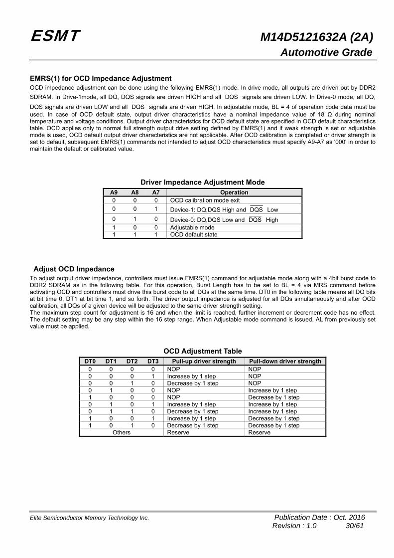
EMRS(1) for OCD Impedance Adjustment OCD impedance adjustment can be done using the following EMRS(1) mode. In drive mode, all outputs are driven out by DDR2 SDRAM. In Drive-1mode, all DQ, DQS signals are driven HIGH and all DQS signals are driven LOW. In Drive-0 mode, all DQ,
DQS signals are driven LOW and all DQS signals are driven HIGH. In adjustable mode, BL = 4 of operation code data must be used. In case of OCD default state, output driver characteristics have a nominal impedance value of 18 Ω during nominal temperature and voltage conditions. Output driver characteristics for OCD default state are specified in OCD default characteristics table. OCD applies only to normal full strength output drive setting defined by EMRS(1) and if weak strength is set or adjustable mode is used, OCD default output driver characteristics are not applicable. After OCD calibration is completed or driver strength is set to default, subsequent EMRS(1) commands not intended to adjust OCD characteristics must specify A9-A7 as '000' in order to maintain the default or calibrated value.
Driver Impedance Adjustment Mode A9 A8 A7 Operation0 0 0 OCD calibration mode exit 0 0 1 Device-1: DQ,DQS High and DQS Low 0 1 0 Device-0: DQ,DQS Low and DQS High 1 0 0 Adjustable mode 1 1 1 OCD default state
Adjust OCD Impedance To adjust output driver impedance, controllers must issue EMRS(1) command for adjustable mode along with a 4bit burst code to DDR2 SDRAM as in the following table. For this operation, Burst Length has to be set to BL = 4 via MRS command before activating OCD and controllers must drive this burst code to all DQs at the same time. DT0 in the following table means all DQ bits at bit time 0, DT1 at bit time 1, and so forth. The driver output impedance is adjusted for all DQs simultaneously and after OCD calibration, all DQs of a given device will be adjusted to the same driver strength setting. The maximum step count for adjustment is 16 and when the limit is reached, further increment or decrement code has no effect. The default setting may be any step within the 16 step range. When Adjustable mode command is issued, AL from previously set value must be applied.
OCD Adjustment Table DT0 DT1 DT2 DT3 Pull-up driver strength Pull-down driver strength
0 0 0 0 NOP NOP 0 0 0 1 Increase by 1 step NOP 0 0 1 0 Decrease by 1 step NOP 0 1 0 0 NOP Increase by 1 step 1 0 0 0 NOP Decrease by 1 step 0 1 0 1 Increase by 1 step Increase by 1 step 0 1 1 0 Decrease by 1 step Increase by 1 step 1 0 0 1 Increase by 1 step Decrease by 1 step 1 0 1 0 Decrease by 1 step Decrease by 1 step
Others Reserve Reserve
ESMT M14D5121632A (2A) Automotive Grade
Elite Semiconductor Memory Technology Inc. Publication Date : Oct. 2016 Revision : 1.0 31/61
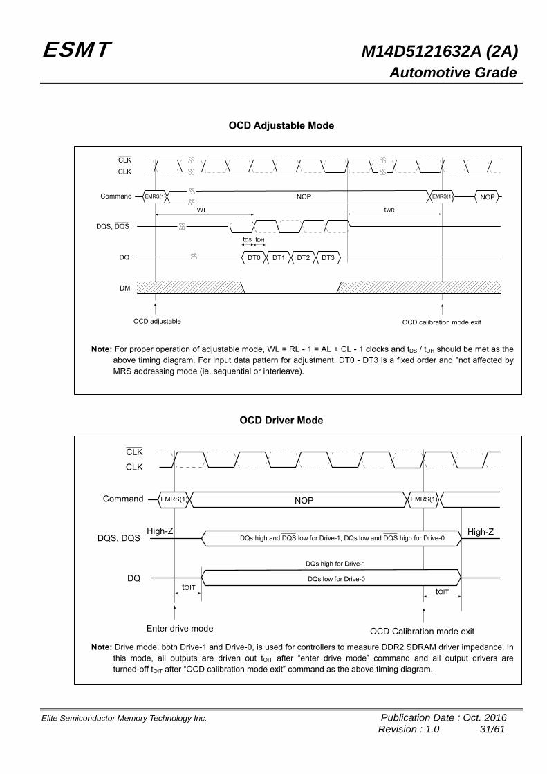
OCD Adjustable Mode
CLK
CLK
EMRS(1) EMRS(1) NOPNOP
DT0
tDS tDH
DT1 DT2 DT3
Command
DQS, DQS
DQ
OCD adjustable OCD calibration mode exit
tWRWL
DM
Note: For proper operation of adjustable mode, WL = RL - 1 = AL + CL - 1 clocks and tDS / tDH should be met as the
above timing diagram. For input data pattern for adjustment, DT0 - DT3 is a fixed order and "not affected by MRS addressing mode (ie. sequential or interleave).
OCD Driver Mode
CLK
CLK
EMRS(1) EMRS(1)NOP
tOIT
Command
DQS, DQS
DQ
Enter drive mode OCD Calibration mode exit
High-ZDQs high and DQS low for Drive-1, DQs low and DQS high for Drive-0
High-Z
DQs low for Drive-0
DQs high for Drive-1
tOIT
Note: Drive mode, both Drive-1 and Drive-0, is used for controllers to measure DDR2 SDRAM driver impedance. In
this mode, all outputs are driven out tOIT after “enter drive mode” command and all output drivers are turned-off tOIT after “OCD calibration mode exit” command as the above timing diagram.

ESMT M14D5121632A (2A) Automotive Grade
Elite Semiconductor Memory Technology Inc. Publication Date : Oct. 2016 Revision : 1.0 32/61
ODT (On Die Termination) On Die Termination (ODT) is a feature that allows a DDR2 SDRAM to turn on/off termination resistance for each DQ, all DQS/ DQS , and all DM signals via the ODT control pin. The ODT feature is designed to improve signal integrity of the memory channel by allowing the DRAM controller to independently turn on/off termination resistance for any or all devices. The ODT function is supported for Active and Standby modes. ODT is turned off and not supported in Self Refresh mode.
Timing for ODT Update Delay
CLK
CLK
EMRS(1)
tAOFD
Command
ODT
InternalRtt Setting
tIS
NOP
tMOD(min.)
tMOD(max.)
Old setting Updating New Setting
Note: tAOFD must be met before issuing EMRS(1) command. ODT must remain low for the entire duration of tMOD window.
ODT Timing for Active and Standby Mode
CLK
CLK
CKE
ODT
InternalTerm Res.
T0 T1 T2 T3 T4 T5 T6
tAOFD
tIS
tAOND
tIS
tAON(min.)tAON(max.) tAOF(min.)
tAOF(max.)
Rtt

ESMT M14D5121632A (2A) Automotive Grade
Elite Semiconductor Memory Technology Inc. Publication Date : Oct. 2016 Revision : 1.0 33/61
ODT Timing for Power-Down Mode
CLK
CLK
CKE
ODT
InternalTerm Res.
T0 T1 T2 T3 T4 T5 T6
tIStIS
tAONPD(min.)tAONPD(max.)
tAOFPD(min.)
Rtt
tAOFPD(max.)

ESMT M14D5121632A (2A) Automotive Grade
Elite Semiconductor Memory Technology Inc. Publication Date : Oct. 2016 Revision : 1.0 34/61
ODT Timing Mode Switch at Entering Power-Down Mode
C K E
C L KC L K
T-5 T-4 T-3 T-2 T-1 T0 T1 T2 T3
tIS
tANPD
Entering slow exit Active Power-Down modeor Precharge Power-Down mode.
Active and Standbymode timings tobe applied.
ODT
InternalTerm Res.
tIS
tAOFD
Rtt
Power-Downmode timings tobe applied.
ODT
InternalTerm Res.
tIS
Rtt
Active and Standbymode timings tobe applied.
ODT
InternalTerm Res.
tIS
Rtt
Power-Downmode timings tobe applied.
ODT
InternalTerm Res.
tIS
Rtt
tAOFPD(max.)
tAOND
tAONPD(max.)

ESMT M14D5121632A (2A) Automotive Grade
Elite Semiconductor Memory Technology Inc. Publication Date : Oct. 2016 Revision : 1.0 35/61
ODT Timing Mode Switch at Exiting Power-Down Mode
C K E
C L KC L K
T0 T1 T4 T5 T6 T7 T8 T9 T10 T11
tIStAXPD
Exiting from slow Active Power-Down modeor Precharge Power-Down mode.
Active and Standbymode timings tobe applied.
ODT
InternalTerm Res.
tIS
tAOFD
Rtt
Power-Downmode timings tobe applied.
ODT
InternalTerm Res.
tIS
Rtt
Active and Standbymode timings tobe applied.
ODT
InternalTerm Res.
tIS
Rtt
Power-Downmode timings tobe applied.
ODT
InternalTerm Res.
tIS
Rtt
tAOFPD(max.)
tAOND
tAONPD(max.)

ESMT M14D5121632A (2A) Automotive Grade
Elite Semiconductor Memory Technology Inc. Publication Date : Oct. 2016 Revision : 1.0 36/61
Precharge The Precharge command is used to precharge or close a bank that has activated. The command is issued when CS , RAS and
WE are LOW and CAS is HIGH at the rising edge of the clock. The Precharge command can be used to precharge each bank respectively or all banks simultaneously. The bank select addresses (BA0, BA1) and A10 are used to define which bank is precharged when the command is initiated. For write cycle, tWR(min.) must be satisfied until the Precharge command can be issued. After tRP from the precharge, a Bank Active command to the same bank can be initiated.
Bank Selection for Precharge by Address bits
A10/AP BA1 BA0 Precharge
0 0 0 Bank A Only
0 1 0 Bank B Only
0 0 1 Bank C Only
0 1 1 Bank D Only
1 X X All Banks
NOP & Device Deselect The device should be deselected by deactivating the CS signal. In this mode, DDR2 SDRAM would ignore all the control inputs.
The DDR2 SDRAM are put in NOP mode when CS is active and by deactivating RAS , CAS and WE . For both Deselect and NOP, the device should finish the current operation when this command is issued.
Bank Active The Bank Active command is issued by holding CAS and WE HIGH with CS and RAS LOW at the rising edge of the clock (CLK). The DDR2 SDRAM has four independent banks, so two Bank Select addresses (BA0, BA1) are required. The Bank Active command to the first Read or Write command must meet or exceed the minimum of RAS to CAS delay time (tRCD(min.)). Once a bank has been activated, it must be precharged before another Bank Active command can be applied to the same bank. The minimum time interval between interleaved Bank Active command (Bank A to Bank B and vice versa) is the Bank to Bank delay time (tRRD min).
Bank Active Command Cycle
CLK
CLK
ACT
tCCD
T0 T1 T2 T3 Tn Tn+1 Tn+2 Tn+3
Command PostedREAD ACT Posted
READ PRE ACT
Bank ARow Addr. Bank BAddress Bank B
Row Addr.Bank B
Col. Addr.Bank A
Row Addr.
Additive latency (AL)tRCD=1
tRRD
Bank ACol. Addr.
tRAStRC
PRE
Bank A
tRP
Bank AActive
Bank BActive
Bank APrecharge
Bank BPrecharge
Bank AActive
Bank A Read begins

ESMT M14D5121632A (2A) Automotive Grade
Elite Semiconductor Memory Technology Inc. Publication Date : Oct. 2016 Revision : 1.0 37/61
Read Bank This command is used after the Bank Active command to initiate the burst read of data. The Read command is initiated by activating CS , CAS , and deasserting WE at the same clock sampling (rising) edge as described in the command truth table.
The length of the burst and the CAS latency time will be determined by the values programmed during the MRS command.
Write Bank This command is used after the Bank Active command to initiate the burst write of data. The Write command is initiated by activating CS , CAS , and WE at the same clock sampling (rising) edge as describe in the command truth table. The length of the burst will be determined by the values programmed during the MRS command.
Posted CAS Posted CAS operation is supported to make command and data bus efficient for sustainable bandwidths in DDR2 SDRAM. In this operation, the DDR2 SDRAM allows a Read or Write command to be issued immediately after the Bank Active command (or any time during the tRRD period). The command is held for the time of the Additive Latency (AL) before it is issued inside the device. The Read Latency (RL) is controlled by the sum of AL and the CAS latency (CL). Therefore if a user chooses to issue a R/W command before the tRCD(min), then AL (greater than 0) must be written into the EMRS(1). The Write Latency (WL) is always defined as RL - 1 (read latency -1) where read latency is defined as the sum of additive latency plus CAS latency (RL=AL+CL). Read or Write operations using AL allow seamless bursts.
Read followed by a Write to the Same Bank
< AL= 2; CL= 3 ; BL = 4>
-1 0 3 4 5 6 7 8 9 10 11 12
CMD
1 2CLK
CLK
ActiveBank A
Dout0 Dout1 Dout2 Dout3 Din0 Din1 Din2 Din3
WL = RL -1 =4AL = 2 CL = 3
>= tRCDRL = AL + CL = 5
DQS/DQS
DQ
ReadBank A
WriteBank A
< AL= 0; CL= 3; BL = 4 >
-1 0 3 4 5 6 7 8 9 10 11 12
CMD
1 2CLK
CLK
WriteBank A
Dout0 Dout1 Dout2 Dout3 Din0 Din1 Din2 Din3
WL = RL -1 = 2
AL = 0
CL = 3
>= tRCDRL = AL + CL = 3
DQS/DQS
DQ
ActiveBank A
ReadBank A

ESMT M14D5121632A (2A) Automotive Grade
Elite Semiconductor Memory Technology Inc. Publication Date : Oct. 2016 Revision : 1.0 38/61
Essential Functionality for DDR2 SDRAM Burst Read Operation The Burst Read command is initiated by having CS and CAS LOW while holding RAS and WE HIGH at the rising edge of the clock. The address inputs determine the starting column address for the burst. The delay from the start of the command to when the data from the first cell appears on the outputs is equal to the value of the read latency (RL). The DQS is driven LOW 1 clock cycle before valid data (DQ) is driven onto the data bus. The first bit of the burst is synchronized with the rising edge of DQS. Each subsequent data-out appears on the DQ pin in phase with the DQS signal in a source synchronous manner. The RL is equal to an additive latency (AL) plus CAS latency (CL). The CL is defined by the MRS and the AL is defined by the EMRS(1).
Read (Data Output) Timing
CLK
CLK
Dout0
tCH
DQS
tDQSQ(max.)
tCL
DQS
DQ Dout1 Dout2 Dout3
tQH
tRPST
tQH
tDQSQ(max.)
tRPRE
Burst Read < RL= 5 (AL= 2; CL= 3); BL= 4 >
CLK
CLK
T0 T1 T2 T3 T4 T5 T6 T7
CMD Posted CASREAD A NOP
AL = 2
T8
NOP NOPNOP NOPNOP NOPNOP
DQS,DQS
CL = 3RL = 5
DoutA0 DoutA1 DoutA2 DoutA3DQs
=< tDQSCK
< RL= 3 (AL= 0; CL= 3); BL= 8 >
CLK
CLK
T0 T1 T2 T3 T4 T5 T6 T7
CMD NOP
T8
NOP NOPNOP NOPNOP NOPNOP
DQS,DQS
CL = 3RL = 3
DoutA4 DoutA5 DoutA6 DoutA7
READ A
DQs DoutA0 DoutA1 DoutA2 DoutA3
=< tDQSCK

ESMT M14D5121632A (2A) Automotive Grade
Elite Semiconductor Memory Technology Inc. Publication Date : Oct. 2016 Revision : 1.0 39/61
Burst Read followed by Burst Write
< RL= 5; WL= (RL-1) = 4; BL= 4 >
CLK
CLK
T0 T1 Tn-1 Tn Tn+1 Tn+2 Tn+3 Tn+4
CMD Posted CASREAD A NOP
Tn+5
NOP NOP NOPNOP NOPNOP
DQS,DQS
WL = RL-1 = 4RL = 5
DoutA0 DoutA1 DoutA2 DoutA3DQs
Posted CASWRITE A
tRTW (Read to Write-turn around-time)
DinA0 DinA1 DinA2 DinA3
Note: The minimum time from the Burst Read command to the Burst Write command is defined by a read to
write-turn around-time(tRTW), which is 4 clocks in case of BL = 4 operation, 6 clocks in case of BL = 8 operation.
Seamless Burst Read
< RL= 5; AL= 2; CL= 3; BL = 4 >
CLK
CLK
T0 T1 T2 T3 T4 T5 T6 T7
CMD Posted CASREAD A
AL = 2
T8
NOP NOPNOP NOPNOP NOPNOP
DQS,DQS
CL = 3RL = 5
DoutA0 DoutA1 DoutA2 DoutA3DQs
Posted CASREAD B
DoutB0 DoutB1 DoutB2
Note: The seamless burst read operation is supported by enabling a Read command at every other clock for BL = 4 operation, and every 4 clock for BL = 8 operation. This operation is allowed regardless of same or different banks as long as the banks are activated.

ESMT M14D5121632A (2A) Automotive Grade
Elite Semiconductor Memory Technology Inc. Publication Date : Oct. 2016 Revision : 1.0 40/61
Burst Write Operation The Burst Write command is issued by having CS , CAS and WE LOW while holding RAS HIGH at the rising edge of the clock (CLK). The address inputs determine the starting column address. Write latency (WL) is defined by a read latency (RL) minus one and is equal to (AL + CL -1); and is the number of clocks of delay that are required from the time the write command is registered to the clock edge associated to the first DQS strobe. A data strobe signal (DQS) should be driven low (preamble) one clock prior to the WL. The first data bit of the burst cycle must be applied to the DQ pins at the first rising edge of the DQS following the preamble. The tDQSS specification must be satisfied for each positive DQS transition to its associated clock edge during write cycles. The subsequent burst bit data are issued on successive edges of the DQS until the burst length is completed, which is 4 or 8 bit burst. When the burst has finished, any additional data supplied to the DQ pins will be ignored. The DQ signal is ignored after the burst write operation is complete. The time from the completion of the burst write to bank precharge is the write recovery time (tWR).
Write (Data Input) Timing
DQSDQS
DQ
tDS
tWPRE
Din0 Din1 Din2 Din3
tDS
DM
tDH tDH
DQS
DQS
tDQSH tDQSL
tWPST
Burst Write < RL= 5 (AL= 2; CL= 3); WL= 4; BL= 4 >
CLK
CLK
T0 T1 T2 T3 T4 T5 T6 T7
CMD Posted CASWRITE A NOP
WL = RL -1 = 4
Tn
NOP NOPNOP NOPNOP PrechargeNOP
DQS,DQS
DinA0 DinA1 DinA2 DinA3DQs
Case1 : with tDQSS(max)
tDSS
WL = RL -1 = 4DQS,DQS
DinA0 DinA1 DinA2 DinA3DQs
tDSHCase2 : with tDQSS(min)
tDQSS
tDQSS
>= tWR
>= tWR
< RL= 3 (AL= 0; CL= 3); WL= 2; BL= 4 >
CLK
CLK
T0 T1 T2 T3 T4 T5 T6 T7
CMD NOP
Tn
NOP NOPNOP NOP Bank AActiveNOPWRITE A
WL = RL -1 = 2DQS,DQS
DinA0 DinA1 DinA2 DinA3DQs
tDQSS
tWR
Precharge
>= tRP

ESMT M14D5121632A (2A) Automotive Grade
Elite Semiconductor Memory Technology Inc. Publication Date : Oct. 2016 Revision : 1.0 41/61
Burst Write followed by Burst Read
< RL= 5 (AL= 2; CL= 3); WL= 4; BL= 4 >
CLK
CLK
T0 T1 T2 T3 T4 T5 T6 T7
CMD NOP
WL = RL -1 = 4
T8
NOP NOP NOPNOP NOP
DQS,DQS
DinA0 DinA1 DinA2 DinA3DQ
Write to Read = CL -1+BL/2+tWTR
> = tWTR
CL = 3
T9
NOP NOPNOP
DQS
DQS
AL = 2
DoutA0
Posted CASREAD A
RL = 5
Note: The minimum number of clock from the Burst Write command to the Burst Read command is [CL - 1 + BL/2 + tWTR]. This tWTR is not a write recovery time (WR) but the time required to transfer the 4 bit write data from the input buffer into sense amplifiers in the array.
Seamless Burst Write
< RL= 5; WL= 4; BL= 4 >
CLK
CLK
T0 T1 T2 T3 T4 T5 T6 T7
CMD
T8
NOP NOPNOP NOPNOP NOPNOP
DQS,DQS
WL = RL-1 = 4
DQs DinA0
Posted CASWRITE A
Posted CASWRITE B
DinA1 DinA2 DinA3 DinB0 DinB1 DinB2 DinB3
Note: The seamless burst write operation is supported by enabling a Write command at every other clock for BL =
4 operation, and every 4 clock for BL = 8 operation. This operation is allowed regardless of same or different banks as long as the banks are activated.

ESMT M14D5121632A (2A) Automotive Grade
Elite Semiconductor Memory Technology Inc. Publication Date : Oct. 2016 Revision : 1.0 42/61
Read Interrupted by a Read Burst Read can only be interrupted by another read with 4 bit burst boundary. Any other case of read interrupt is not allowed.
< CL= 3; AL= 0; RL= 3; BL= 8 >
CLK
CLK
CMD NOP NOP NOPNOP NOPNOP
DQS,DQS
DQs A0
READ A READ B NOP
A1 A3A2 B0 B3B2B1 B4 B7B6B5
NOP
Note: 1. Read burst interrupt function is only allowed on burst of 8. Burst interrupt of 4 is prohibited. 2. Read burst of 8 can only be interrupted by another Read command. Read burst interruption by Write command or Precharge command is prohibited. 3. Read burst interrupt must occur exactly two clocks after previous Read command. Any other Read burst interrupt timings are prohibited. 4. Read burst interruption is allowed to any bank inside DRAM. 5. Read burst with Auto Precharge enabled is not allowed to interrupt. 6. Read burst interruption is allowed by another Read with Auto Precharge command. 7. All command timings are referenced to burst length set in the mode register. They are not referenced to actual burst. For example, Minimum Read to Precharge timing is AL + BL/2 where BL is the burst length set in the MRS and not the actual burst (which is shorter because of interrupt).

ESMT M14D5121632A (2A) Automotive Grade
Elite Semiconductor Memory Technology Inc. Publication Date : Oct. 2016 Revision : 1.0 43/61
Write Interrupted by a Write Burst Wirte can only be interrupted by another Write with 4 bit burst boundary. Any other case of Write interrupt is not allowed.
< CL= 3; AL= 0; RL= 3; WL= 2; BL= 8 >
CLK
CLK
T0 T1 T2 T3 T4 T5 T6 T7
CMD
T8
Write A NOP NOPNOP NOPNOP
DQS,DQS
DQs A0
NOP NOP NOP
A1 A3A2 B0 B3B2B1 B4 B7B6B5
Write B
Note: 1. Write burst interrupt function is only allowed on burst of 8. Burst interrupt of 4 is prohibited. 2. Write burst of 8 can only be interrupted by another Write command. Write burst interruption by Read command or Precharge command is prohibited. 3. Write burst interrupt must occur exactly two clocks after previous Write command. Any other Write burst interrupt timings are prohibited. 4. Write burst interruption is allowed to any bank inside DRAM. 5. Write burst with Auto Precharge enabled is not allowed to interrupt. 6. Write burst interruption is allowed by another Write with Auto Precharge command. 7. All command timings are referenced to burst length set in the MRS. They are not referenced to actual burst. For example, minimum Write to Precharge timing is WL+BL/2+ tWR where tWR starts with the rising clock after the un-interrupted burst end and not from the end of actual burst end.

ESMT M14D5121632A (2A) Automotive Grade
Elite Semiconductor Memory Technology Inc. Publication Date : Oct. 2016 Revision : 1.0 44/61
Burst Read Followed by Precharge
Minimum Read to Precharge command spacing to the same bank = AL + BL/2 + max(tRTP, 2) - 2 clocks. For the earliest possible Precharge, the Precharge command may be issued on the rising edge which is “Additive latency (AL) + BL/2 clocks” after a Read command. A new Bank Active command may be issued to the same bank after the Precharge time (tRP). A Precharge command cannot be issued until tRAS is satisfied. The minimum Read to Precharge spacing has also to satisfy a minimum analog time from the rising clock edge that initiates the last 4-bit prefetch of a Read to Precharge command. This time is called tRTP (Read to Precharge). For BL = 4, this is the time from the actual read (AL after the Read command) to Precharge command. For BL = 8, this is the time from AL + 2 clocks after the Read to the Precharge command.
< RL= 4 (AL= 1; CL= 3) >
CLK
CLK
T0 T1 T2 T3 T4 T5 T6 T7
CMD Posted CASREAD A NOP
AL + BL/2 clks
T8
NOP NOP NOPNOPPrecharge Bank AActive
DQS,DQS
DoutA0DQs
>= tRP
NOP
AL = 1 CL = 3RL = 4
DoutA1 DoutA2 DoutA3>= tRAS
CL = 3>= tRTP
CMD Posted CASREAD A NOP
AL + BL/2 clksNOP NOPNOP NOPPrecharge A
DQS,DQS
DoutA0DQs
NOP
AL = 1 CL = 3RL = 4
DoutA1 DoutA2 DoutA3 DoutA4 DoutA5 DoutA6 DoutA7
>= tRTP
NOP
BL = 8
BL = 4
< RL= 5 (AL= 2; CL= 3); BL= 4 >
CLK
CLK
T0 T1 T2 T3 T4 T5 T6 T7
CMD Posted CASREAD A NOP
AL + BL/2 clks
T8
NOP NOP NOPNOPPrecharge A Bank AActive
DQS,DQS
DoutA0DQs
>= tRP
NOP
AL = 2 CL = 3RL = 5
DoutA1 DoutA2 DoutA3>= tRAS
CL = 3>= tRTP < RL= 6 (AL= 2; CL= 4); BL= 4 >
CLK
CLK
T0 T1 T2 T3 T4 T5 T6 T7
CMD Posted CASREAD A NOP
AL + BL/2 clks
T8
NOP NOP NOPNOPPrecharge A Bank AActive
DQS,DQS
DoutA0DQs
>= tRP
NOP
AL = 2 CL = 4RL = 6
DoutA1 DoutA2 DoutA3>= tRAS
CL = 4>= tRTP

ESMT M14D5121632A (2A) Automotive Grade
Elite Semiconductor Memory Technology Inc. Publication Date : Oct. 2016 Revision : 1.0 45/61
< RL= 4 (AL= 0; CL= 4); BL=8 >
CLK
CLK
CMD NOP NOPNOP NOPPrecharg A Bank AActiveNOP
DQS,DQS
AL+2 clks + max(tRTP;2)
DQs
Posted CASWRITE A
T0 T1 T2 T3 T4 T5 T6 T7 T8
NOP
> = tRP
CL = 4AL = 0
>= tRAS
DoutA0 DoutA1 DoutA2 DoutA3 DoutA4 DoutA5 DoutA6 DoutA7
RL = 4
Burst Write Followed by Precharge
Minimum Write to Precharge command spacing to the same bank = WL + BL/2 clocks + tWR. For write cycles, a delay must be satisfied from the completion of the last burst write cycle until the Precharge command can be issued. This delay is known as a write recovery time (tWR) referenced from the completion of the Burst Write to the Precharge command. No Precharge command should be issued prior to the tWR delay.
< WL= (RL-1) = 3; BL=4>
CLK
CLK
CMD NOP NOPNOP NOP Precharg ANOP
DQS,DQS
DQs
Posted CASWRITE A
T0 T1 T2 T3 T4 T5 T6 T7 T8
NOP
> = tWR
WL = 3
DinA0
NOP
DinA1 DinA2 DinA3
< WL= (RL-1) = 4; BL=4 >
CLK
CLK
CMD NOP NOPNOP NOP Precharg ANOP
DQS,DQS
DQs
Posted CASWRITE A
T0 T1 T2 T3 T4 T5 T6 T7 T9
NOP
> = tWR
WL = 4
DinA0
NOP
DinA1 DinA2 DinA3

ESMT M14D5121632A (2A) Automotive Grade
Elite Semiconductor Memory Technology Inc. Publication Date : Oct. 2016 Revision : 1.0 46/61
Write data mask by DM One write data mask (DM) pin for each 8 data bits (DQ) will be supported on DDR2 SDRAM, Consistent with the implementation on DDR2 SDRAM. It has identical timings on write operations as the data bits, and though used in a uni-directional manner, is internally loaded identically to data bits to insure matched system timing. DM is not used during read cycles.
Data Mask Timing
DQS
DQS
T1 T2 T3 T4 T5 Tn
DQ
DM
Din Din Din Din Din Din Din Din Din
Write mask Iatency = 0
Example: < WL= 3; AL= 0; BL= 4 >
CLK
CLK
T0 T1 T2 T3 T4 T5 T6 T7
Command
WL
T8
DQS,DQS
Din0DQ
tWRNOPWRIT
tDQSS
Din2
DM
[tDQSS(min.)]
WL
DQS,DQS
Din0DQ
tDQSS
Din2
DM
[tDQSS(max.)]

ESMT M14D5121632A (2A) Automotive Grade
Elite Semiconductor Memory Technology Inc. Publication Date : Oct. 2016 Revision : 1.0 47/61
Read with Auto Precharge If A10 is HIGH when a Read command is issued, the Read with Auto Precharge function is engaged. The device starts an Auto Precharge operation on the rising edge which is (AL + BL/2) cycles later than the Read with AP command if tRAS (min) and tRTP(min) are satisfied. If tRAS(min) is not satisfied at the edge, the start point of Auto Precharge operation will be delayed until tRAS(min) is satisfied. If tRTP (min) is not satisfied at the edge, the start point of Auto Precharge operation will be delayed until tRTP (min) is satisfied. In case the internal precharge is pushed out by tRTP, tRP starts at the point where the internal precharge happens (not at the next rising clock edge after this event). So for BL = 4, the minimum time from Read_AP to the next Bank Active command becomes AL + (tRTP + tRP)*. For BL = 8, the time from Read_AP to the next Bank Active command is AL + 2 + (tRTP + tRP)*. (Note: “*” means “rouded up to the next integer”).
< RL= 4 (AL= 1; CL= 3) >
CLK
CLK
T0 T1 T2 T3 T4 T5 T6 T7
CMD
T8
NOP NOPNOP NOPNOP Bank AActiveNOP
DQS,DQS
DQs
Posted CASREAD A NOP
AL+BL/2 clks > = tRPAutoprecharge
CL = 3AL = 1
>= tRTP
DoutA0 DoutA1 DoutA2 DoutA3 DoutA4 DoutA5 DoutA6 DoutA7
RL = 4
tRTP
Precharge begins here
BL = 8t RTP <= 2 clocks
CMD NOP NOPNOP NOPNOP Bank AActive NOP
DQS,DQS
DQs
Posted CASREAD A NOP
>=AL+tRTP+tRPAutoprecharge
CL = 3AL = 1
tRP
DoutA0 DoutA1 DoutA2 DoutA3
RL = 4
tRTP
Precharge begins here
BL = 4t RTP > 2 clocks
A new Bank Active command may be issued to the same bank if the following two conditions are satisfied simultaneously. (1) The Precharge time (tRP) has been satisfied from the clock at which the Auto Precharge begins. (2) The RAS cycle time (tRC) from the previous bank activation has been satisfied.

ESMT M14D5121632A (2A) Automotive Grade
Elite Semiconductor Memory Technology Inc. Publication Date : Oct. 2016 Revision : 1.0 48/61
< RL= 5 (AL= 2; CL= 3); BL= 4; tRCD = 3 clocks; tRTP <= 2 clocks >
CLK
CLK
T0 T1 T2 T3 T4 T5 T6 T7
CMD Posted CASREAD A NOP
>= tRAS(min)
T8
NOP NOP NOPNOP Bank AActive
DQS,DQS
DoutA0DQs
>= tRP
NOP
AL = 2 CL = 3RL = 5
DoutA1 DoutA2 DoutA3
>= tRC
tRC Limit
NOPAutoprecharge
Autoprecharge begins
CLK
CLK
CMD Posted CASREAD A NOP
>= tRAS(min)
NOP NOP NOPNOP Bank AActive
DQS,DQS
DoutA0DQs
>= tRP
NOP
AL = 2 CL = 3RL = 5
DoutA1 DoutA2 DoutA3
tRP Limit
NOPAutoprecharge
Autoprecharge begins
>= tRC
Write with Auto Precharge If A10 is HIGH when a Write command is issued, the Write with Auto Precharge function is engaged (If tCK < 1.875ns, the device can not support Write with Auto Precharge function). The device automatically begins precharge operation after the completion of the burst write plus write recovery time (tWR). The Bank Active command undergoing Auto Precharge from the completion of the write burst may be reactivated if the following two conditions are satisfied. (1) The data-in to bank activate delay time (tWR + tRP) has been satisfied. (2) The RAS cycle time (tRC) from the previous bank activation has been satisfied.
< WR = 2; BL= 4; tRP = 3 clocks >
CLK
CLK
T0 T1 T2 T3 T4 T5 T6 T7
CMD Posted CASWRITE A NOP
Tm
NOP NOP NOPNOP Bank AActive
DQS,DQS
DinA0DQs
>= tRP
NOP
WL = RL-1 = 2
>= tRC
tRC Limit
NOPAutoprecharge
Auto Precharge begins
CLK
CLK
CMD Posted CASWRITE A NOPNOP NOP NOPNOP Bank A
Active
DQS,DQS
DinA0DQs
NOP
DinA1 DinA2 DinA3
>= tRC
tWR + tRP
NOPAutoprecharge
DinA1 DinA2 DinA3
>= tWR
T0 T3 T4 T5 T6 T7 T8 T9 T12
Auto Precharge begins
>= tRP>= tWRWL = RL-1 = 4

ESMT M14D5121632A (2A) Automotive Grade
Elite Semiconductor Memory Technology Inc. Publication Date : Oct. 2016 Revision : 1.0 49/61
Auto Refresh & Self Refresh Auto Refresh An Auto Refresh command is issued by having CS , RAS and CAS held LOW with CKE and WE HIGH at the rising edge of the clock(CLK). All banks must be precharged and idle for tRP(min) before the Auto Refresh command is applied. An address counter, internal to the device, supplies the bank address during the refresh cycle. No control of the external address bus is required once this cycle has started. When the refresh cycle has completed, all banks will be in the idle state. A delay between the Auto Refresh command and the next Bank Active command or subsequent Auto Refresh command must be greater than or equal to the tRFC(min).To allow for improved efficiency in scheduling and switching between tasks, some flexibility in the absolute refresh interval is provided. A maximum of eight Refresh commands can be posted, meaning that the maximum absolute interval between any Refresh command and the next Refresh command is 9 x tREFI.
C O M M A N D
C K E = H i g h
t R P
P R E AutoRefresh C M D
t R F C
C L KC L K

ESMT M14D5121632A (2A) Automotive Grade
Elite Semiconductor Memory Technology Inc. Publication Date : Oct. 2016 Revision : 1.0 50/61
Self Refresh A Self Refresh command is defined by having CS , RAS , CAS and CKE held LOW with WE HIGH at the rising edge of the clock (CLK). ODT must be turned off before issuing Self Refresh command, by either driving ODT pin low or using EMRS(1) command. Once the command is registered, CKE must be held LOW to keep the device in Self Refresh mode. The DLL is automatically disabled upon entering Self Refresh and is automatically enabled upon exiting Self Refresh. When the device has entered Self Refresh mode, all of the external signals except CKE, are “don’t care”. For proper Self Refresh operation all power supply pins (VDD, VDDQ, VDDL and VREF) must be at valid levels. The device initiates a minimum of one refresh command internally within tCKE period once it enters Self Refresh mode. The clock is internally disabled during Self Refresh operation to save power. Self Refresh mode must be remained tCKE (min). The user may change the external clock frequency or halt the external clock one clock after Self Refresh entry is registered, however, the clock must be restarted and stable before the device can exit Self Refresh operation. The procedure for exiting Self Refresh requires a sequence of commands. First, the clock must be stable prior to CKE going back HIGH. Once Self Refresh Exit is registered, a delay of tXSRD(min) must be satisfied before a valid command can be issued to the device to allow for any internal refresh in progress. CKE must remain HIGH for the entire Self Refresh exit period tXSRD for proper operation except for Self Refresh re-entry. Upon exit from Self Refresh, the device can be put back into Self Refresh mode after waiting tXSNR(min) and issuing one Refresh command. NOP or deselect commands must be registered on each positive clock edge during the Self Refresh exit interval tXSNR. ODT should be turned off during tXSRD. The use of Self Refresh mode introduces the possibility that an internally timed refresh event can be missed when CKE is raised for exit from Self Refresh mode. Upon exit from Self Refresh, the device requires a minimum of one extra auto refresh command before it is put back into Self Refresh mode. If TC > +95 , the device can’t support Self refresh function.
CLK
CLK
T0 T1 T2 T3 T4 T5 T6 Tn
CKE
Tm
ODT
>= tXSNRtRP
Command
tAOFD
>= tXSRD
tIS tIS
tIS tIHtIS
tCK
tCH tCL
Note: 1. Device must be in the “All banks idle” state prior to entering Self Refresh mode. 2. ODT must be turned off tAOFD before entering Self Refresh mode, and can be turned on again when tXSRD
timing is satisfied. 3. tXSRD is applied for a Read or a Read with Auto Precharge command. 4. tXSNR is applied for any command except a Read or a Read with Auto Precharge command.

ESMT M14D5121632A (2A) Automotive Grade
Elite Semiconductor Memory Technology Inc. Publication Date : Oct. 2016 Revision : 1.0 51/61
Power-Down Power-Down is synchronously entered when CKE is registered LOW (no accesses can be in progress). CKE is not allowed to go LOW while MRS or EMRS command time, or read or write operation is in progress. CKE is allowed to go LOW while any of other operations such as Bank Active, Precharge or Auto Precharge, or Auto Refresh is in progress. The DLL should be in a locked state when Power-Down is entered. Otherwise DLL should be reset after exiting Power-Down mode for proper read operation. If Power-Down occurs when all banks are idle, this mode is referred to as Precharge Power-Down; if Power-Down occurs when there is a Bank Active command in any bank, this mode is referred to as Active Power-Down. Entering Power-Down deactivates the input and output buffers, excluding CLK, CLK , ODT and CKE. Also the DLL is disabled upon entering Precharge Power-Down or slow exit Active Power-Down, but the DLL is kept enabled during fast exit Active Power-Down. In Power-Down mode, CKE LOW and a stable clock signal must be maintained at the inputs of the device, and ODT should be in a valid state but all other input signals are “Don’t Care”. CKE LOW must be maintained until tCKE has been satisfied. Power-Down duration is limited by 9 times tREFI of the device. The Power-Down state is synchronously exited when CKE is registered HIGH (along with a NOP or DESELECT command). CKE HIGH must be maintained until tCKE has been satisfied. A valid, executable command can be applied with Power-Down exit latency, tXP, tXARD, or tXARDS, after CKE goes HIGH.
CLK
CLK
CKE
Command VALID
tIS tIH tIS tIH tIH tIS tIH
NOP NOP VALID VALIDVALID
tCKE tCKE
Enter power-down mode
tXP, tXARD,tXARDS
Exit power-down mode tCKE
: Don’t care
Read to Power-Down Entry
CLK
CLK
Command READ
CKE
CKE should be kept high until the end of burst operation
DQ
T0 T1 T2 Tx Tx+1 Tx+2 Tx+3
High
AL + CLDoutA0 DoutA1 DoutA2 DoutA3
Tx+4 Tx+5 Tx+6 Tx+7 Tx+8 Tx+9
DQSDQS
BL = 4
CLK
CLK
Command READ
CKE
CKE should be kept high until the end of burst operation
DQ
T0 T1 T2 Tx Tx+1 Tx+2 Tx+3
High
AL + CLDoutA0 DoutA1 DoutA2 DoutA3
Tx+4 Tx+5 Tx+6 Tx+7 Tx+8 Tx+9
DQSDQS
BL = 8
DoutA4 DoutA5 DoutA6 DoutA7

ESMT M14D5121632A (2A) Automotive Grade
Elite Semiconductor Memory Technology Inc. Publication Date : Oct. 2016 Revision : 1.0 52/61
Read with Auto Precharge to Power-Down Entry
CLK
CLK
Command READ
CKE
CKE should be kept high until the end of burst operation
DQ
T0 T1 T2 Tx Tx+1 Tx+2 Tx+3
AL+BL/2with tRTP =7.5nsand tRAS(min.) satisfied
AL + CLDoutA0 DoutA1 DoutA2 DoutA3
Tx+4 Tx+5 Tx+6 Tx+7 Tx+8 Tx+9
DQSDQS
BL = 4
CLK
CLK
Command READ
CKE
CKE should be kept high until the end of burst operation
DQ
T0 T1 T2 Tx Tx+1 Tx+2 Tx+3
AL + CLDoutA0 DoutA1 DoutA2 DoutA3
Tx+4 Tx+5 Tx+6 Tx+7 Tx+8 Tx+9
DQSDQS
BL = 8
DoutA4 DoutA5 DoutA6 DoutA7
PRE
PRE
Start internal precharge
AL+BL/2with tRTP = 7.5nsand tRAS(min.) satisfied
Write to Power-Down Entry
CLK
CLK
Command WRITE
CKE
DQ
T0 T1 Tm Tm+1 Tm+2 Tm+3 Tx
WL
DinA0 DinA1 DinA2 DinA3
Tx+1 Tx+2 Ty Ty+1 Ty+2 Ty+3
DQSDQS
BL = 4
CLK
CLK
Command WRITE
CKE
DQ
T0 T1 Tm Tm+1 Tm+2 Tm+3 Tm+4
DinA0 DinA1
Tm+5 Tx Tx+1 Tx+2 Tx+3 Tx+4
DQSDQS
BL = 8
tWTR
DinA2 DinA3 DinA4 DinA5 DinA6 DinA7
tWTR
WL

ESMT M14D5121632A (2A) Automotive Grade
Elite Semiconductor Memory Technology Inc. Publication Date : Oct. 2016 Revision : 1.0 53/61
Write with Auto Precharge to Power-Down Entry
CLK
CLK
Command WRITE A
CKE
DQ
T0 T1 Tm Tm+1 Tm+2 Tm+3 Tx
WL
DinA0 DinA1 DinA2 DinA3
Tx+1 Tx+2 Tx+3 Tx+4 Tx+5 Tx+6
DQSDQS
BL = 4
CLK
CLK
Command WRITE A
CKE
DQ
T0 T1 Tm Tm+1 Tm+2 Tm+3 Tm+4
DinA0 DinA1
Tm+5 Tx Tx+1 Tx+2 Tx+3 Tx+4
DQSDQS
BL = 8
tWR
DinA2 DinA3 DinA4 DinA5 DinA6 DinA7
tWR
WL
PRE
PRE
Note: If tCK < 1.875ns, the device can not support Write with Auto Precharge function.
Auto Refresh/ Bank Active/ Precharge to Power-Down Entry
CLK
CLK
Command CMD
CKE
T0 T1 T2 T3 T4 T5 T6 T7 T8 T9 T10 T11
CKE can go to low one clock after a command
Note: CMD could be Auto Refresh/ Bank Active/ Precharge command.
MRS/EMRS to Power-Down Entry
CLK
CLK
T0 T1 T2 T3 T4 T5 T6 T7 T8 T9 T10 T11
CKE
MRS/EMRSCommand
tMRD

ESMT M14D5121632A (2A) Automotive Grade
Elite Semiconductor Memory Technology Inc. Publication Date : Oct. 2016 Revision : 1.0 54/61
Asynchronous CKE Low event DDR2 SDRAM requires CKE to be maintained “HIGH” for all valid operations as defined in this data sheet. If CKE asynchronously drops “LOW” during any valid operation, the device is not guaranteed to preserve the contents of array. If this event occurs, memory controller must satisfy tDELAY before turning off the clocks. Stable clocks must exist at the input of device before CKE is raised “HIGH” again. The device must be fully re-initialized (steps 4 ~ 13) as described in initialization sequence. The device is ready for normal operation after the initialization sequence.
CLK
CLK
CKE
tCK
tDELAY
Stable clocks
CKE asynchronouslydrops low Clocks can be turned off
after this point
Clock Frequency change in Precharge Power-Down mode DDR2 SDRAM input clock frequency can be changed under following condition: The device is in Precharge Power-Down mode. ODT must be turned off and CKE must be at logic LOW level. A minimum of 2 clocks must be waited after CKE goes LOW before clock frequency may change. The device input clock frequency is allowed to change only between tCK (min) and tCK (max). During input clock frequency change, ODT and CKE must be held at stable LOW levels. Once input clock frequency is changed, stable new clocks must be provided before Precharge Power-Down may be exited and DLL must be RESET via MRS after Precharge Power-Down exit. Depending on new clock frequency an additional MRS command may need to be issued to appropriately set the WR, CL etc.. During DLL re-lock period, ODT must remain off. After the DLL lock time, the device is ready to operate with new clock frequency.
CLK
CLK
Minimum 2 clocks requiredbefore changing frequency
T0 T1 T2 T4
tRP
Tx Tx+1 Ty Ty+1 Ty+2 Ty+3 Ty+4 Tz
CKE
ODT
NOPcommand NOP NOP NOP DLLReset NOP Vaild
tAOFD txP
200 clocksFrequency change
occurs here
Stable new clockbefore power down exit
ODT is offduring DLL RESET

ESMT M14D5121632A (2A) Automotive Grade
Elite Semiconductor Memory Technology Inc. Publication Date : Oct. 2016 Revision : 1.0 55/61
Functional Truth Table *7
Current State CS RAS CAS WE Address Command Action
IDLE
H X X X X DESEL NOP or Power-Down
L H H H X NOP NOP or Power-Down
L H L X BA, CA, A10 READ / READA / WRITE / WRITEA ILLEGAL (*1)
L L H H BA, RA Active Bank Active, Latch RA
L L H L BA, A10 / A10 PRE / PREA Precharge / Precharge All
L L L H X Refresh Refresh (*2)
L L L L Op-Code Mode-Add MRS / EMRS Mode Register setting / Extended Mode Register setting (*2)
BANK ACTIVE
H X X X X DESEL NOP
L H H H X NOP NOP
L H L H BA, CA, A10 READ / READA Begin Read, Latch CA, Determine Auto Precharge
L H L L BA, CA, A10 WRITE / WRITEA Begin Write, Latch CA, Determine Auto Precharge
L L H H BA, RA Active ILLEGAL (*1)
L L H L BA, A10 /A10 PRE / PREA Precharge / Precharge All
L L L H X Refresh ILLEGAL
L L L L Op-Code Mode-Add MRS / EMRS ILLEGAL
READ
H X X X X DESEL NOP (Continue Burst to END)
L H H H X NOP NOP (Continue Burst to END)
L H L H BA, CA, A10 READ / READA Terminate Burst, Latch CA, Begin New Read, Determine Auto Precharge (*1, 4)
L H L L BA, CA, A10 WRITE / WRITEA ILLEGAL (*1)
L L H H BA, RA Active ILLEGAL (*1)
L L H L BA, A10 / A10 PRE / PREA ILLEGAL (*1) / ILLEGAL
L L L H X Refresh ILLEGAL
L L L L Op-Code Mode-Add MRS / EMRS ILLEGAL
WRITE
H X X X X DESEL NOP (Continue Burst to end)
L H H H X NOP NOP (Continue Burst to end)
L H L H BA, CA, A10 READ / READA ILLEGAL (*1)
L H L L BA, CA, A10 WRITE / WRITEA Terminate Burst, Latch CA, Begin new Write, Determine Auto-Precharge (*1, 4)
L L H H BA, RA Active ILLEGAL (*1)
L L H L BA, A10 / A10 PRE / PREA ILLEGAL (*1) / ILLEGAL
L L L H X Refresh ILLEGAL
L L L L Op-Code Mode-Add MRS / EMRS ILLEGAL
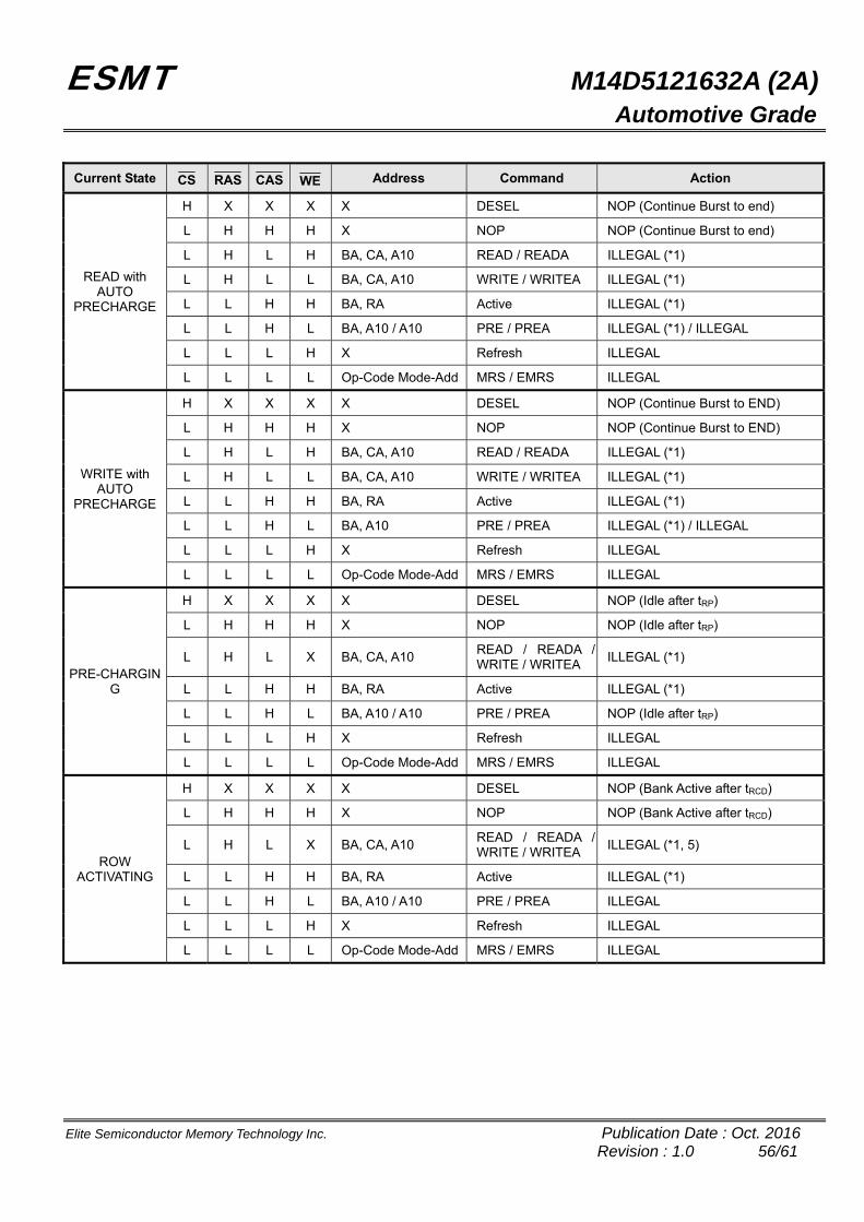
ESMT M14D5121632A (2A) Automotive Grade
Elite Semiconductor Memory Technology Inc. Publication Date : Oct. 2016 Revision : 1.0 56/61
Current State CS RAS CAS WE Address Command Action
READ with AUTO
PRECHARGE
H X X X X DESEL NOP (Continue Burst to end)
L H H H X NOP NOP (Continue Burst to end)
L H L H BA, CA, A10 READ / READA ILLEGAL (*1)
L H L L BA, CA, A10 WRITE / WRITEA ILLEGAL (*1)
L L H H BA, RA Active ILLEGAL (*1)
L L H L BA, A10 / A10 PRE / PREA ILLEGAL (*1) / ILLEGAL
L L L H X Refresh ILLEGAL
L L L L Op-Code Mode-Add MRS / EMRS ILLEGAL
WRITE with AUTO
PRECHARGE
H X X X X DESEL NOP (Continue Burst to END)
L H H H X NOP NOP (Continue Burst to END)
L H L H BA, CA, A10 READ / READA ILLEGAL (*1)
L H L L BA, CA, A10 WRITE / WRITEA ILLEGAL (*1)
L L H H BA, RA Active ILLEGAL (*1)
L L H L BA, A10 PRE / PREA ILLEGAL (*1) / ILLEGAL
L L L H X Refresh ILLEGAL
L L L L Op-Code Mode-Add MRS / EMRS ILLEGAL
PRE-CHARGING
H X X X X DESEL NOP (Idle after tRP)
L H H H X NOP NOP (Idle after tRP)
L H L X BA, CA, A10 READ / READA / WRITE / WRITEA ILLEGAL (*1)
L L H H BA, RA Active ILLEGAL (*1)
L L H L BA, A10 / A10 PRE / PREA NOP (Idle after tRP)
L L L H X Refresh ILLEGAL
L L L L Op-Code Mode-Add MRS / EMRS ILLEGAL
ROW ACTIVATING
H X X X X DESEL NOP (Bank Active after tRCD)
L H H H X NOP NOP (Bank Active after tRCD)
L H L X BA, CA, A10 READ / READA / WRITE / WRITEA ILLEGAL (*1, 5)
L L H H BA, RA Active ILLEGAL (*1)
L L H L BA, A10 / A10 PRE / PREA ILLEGAL
L L L H X Refresh ILLEGAL
L L L L Op-Code Mode-Add MRS / EMRS ILLEGAL

ESMT M14D5121632A (2A) Automotive Grade
Elite Semiconductor Memory Technology Inc. Publication Date : Oct. 2016 Revision : 1.0 57/61
Current State CS RAS CAS WE Address Command Action
WRITE RECOVERING
H X X X X DESEL NOP (Bank Active after tWR)
L H H H X NOP NOP (Bank Active after tWR)
L H L H BA, CA, A10 READ / READA ILLEGAL (*1, 6)
L H L L BA, CA, A10 WRITE / WRITEA WRITE / WRITEA
L L H H BA, RA Active ILLEGAL (*1)
L L H L BA, A10 / A10 PRE / PREA ILLEGAL (*1) / ILLEGAL
L L L H X Refresh ILLEGAL
L L L L Op-Code Mode-Add MRS / EMRS ILLEGAL
WRITE RECOVERING
with
AUTO PRECHARGE
H X X X X DESEL NOP (Bank Active after tWR)
L H H H X NOP NOP (Bank Active after tWR)
L H L X BA, CA, A10 READ / READA / WRITE / WRITEA ILLEGAL (*1)
L L H H BA, RA Active ILLEGAL (*1)
L L H L BA, A10 / A10 PRE / PREA ILLEGAL (*1) / ILLEGAL
L L L H X Refresh ILLEGAL
L L L L Op-Code Mode-Add MRS / EMRS ILLEGAL
REFRESH
H X X X X DESEL NOP (Idle after tRFC)
L H H H X NOP NOP (Idle after tRFC)
L H L X BA, CA, A10 READ / READA / WRITE / WRITEA ILLEGAL
L L H H BA, RA Active ILLEGAL
L L H L BA, A10 / A10 PRE / PREA ILLEGAL
L L L H X Refresh ILLEGAL
L L L L Op-Code Mode-Add MRS / EMRS ILLEGAL
(Extended) MODE
REGISTER SETTING
H X X X X DESEL NOP (Idle after tMRD)
L H H H X NOP NOP (Idle after tMRD)
L H L X BA, CA, A10 READ / READA / WRITE / WRITEA ILLEGAL
L L H H BA, RA Active ILLEGAL
L L H L BA, A10 / A10 PRE / PREA ILLEGAL
L L L H X Refresh ILLEGAL
L L L L Op-Code Mode-Add MRS / EMRS ILLEGAL H = High Level, L = Low level, X = Don’t Care BA = Bank Address, RA =Row Address, CA = Column Address, NOP = No Operation ILLEGAL = Device operation and / or data integrity are not guaranteed.
Note:
1. This command may be issued for other banks, depending on the state of the banks. 2. All banks must be in “IDLE”. 3. All AC timing specs must be met. 4. Only allowed at the boundary of 4 bits burst. Burst interruption at other timings is illegal. 5. Available in case tRCD is satisfied by AL setting. 6. Available in case tWTR is satisfied. 7. If tCK < 1.875ns, the device can not support Write with Auto Precharge function.

ESMT M14D5121632A (2A) Automotive Grade
Elite Semiconductor Memory Technology Inc. Publication Date : Oct. 2016 Revision : 1.0 58/61
Simplified States Diagram
Power-Up and InitializationSequence
OCDcalibration
Settign MRS
EMRS
SelfRefreshing
Idle
All banksprecharged
Refreshing
PrechargePower-Down
SRF
REF
CKEH
CKEL
Activating
(E)MRS
PR
BankActive
ActivePower-Down
CKEH
CKEL
CKEL
CKEL
CKEL
CKEL
CKEL
ReadingWrite
WriteRead
ReadingWith
Auto PrechargeWriting
WithAuto Precharge
Precharging
Write
WriteRead
RDA
RDA
RDA
WRA
WRA
WRA
PR, PRA PR, PRAPR, PRA
Read
CKEH
ACT
Automatic Sequence
Command Sequence
CKEL = CKE LOW CKEH = CKE HIGH ACT = Activate WR(A) = Write (with Auto Precharge) RD(A) = Read (with Auto Precharge) PR(A) = Precharge (All) (E)MRS = (Extended) Mode Register Set SRF = Enter Self Refresh REF = Auto Refresh
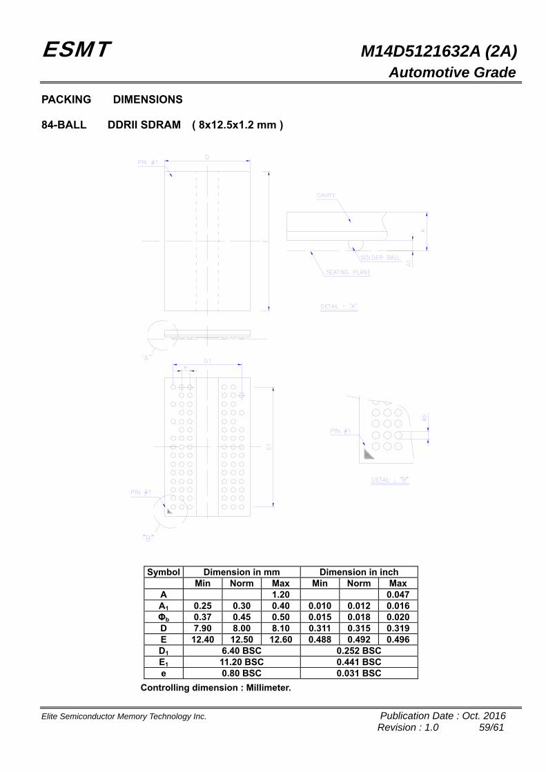
ESMT M14D5121632A (2A) Automotive Grade
Elite Semiconductor Memory Technology Inc. Publication Date : Oct. 2016 Revision : 1.0 59/61
PACKING DIMENSIONS 84-BALL DDRII SDRAM ( 8x12.5x1.2 mm )
Symbol Dimension in mm Dimension in inch Min Norm Max Min Norm Max
A 1.20 0.047 A1 0.25 0.30 0.40 0.010 0.012 0.016 Φb 0.37 0.45 0.50 0.015 0.018 0.020 D 7.90 8.00 8.10 0.311 0.315 0.319 E 12.40 12.50 12.60 0.488 0.492 0.496 D1 6.40 BSC 0.252 BSCE1 11.20 BSC 0.441 BSCe 0.80 BSC 0.031 BSC
Controlling dimension : Millimeter.

ESMT M14D5121632A (2A) Automotive Grade
Elite Semiconductor Memory Technology Inc. Publication Date : Oct. 2016 Revision : 1.0 60/61
Revision History
Revision Date Description
0.1 2016.07.07 Original
1.0 2016.10.07 1. Delete "Preliminary"
2. Update Input / Output Capacitance

ESMT M14D5121632A (2A) Automotive Grade
Elite Semiconductor Memory Technology Inc. Publication Date : Oct. 2016 Revision : 1.0 61/61
Important Notice
All rights reserved. No part of this document may be reproduced or duplicated in any form or by any means without the prior permission of ESMT. The contents contained in this document are believed to be accurate at the time of publication. ESMT assumes no responsibility for any error in this document, and reserves the right to change the products or specification in this document without notice. The information contained herein is presented only as a guide or examples for the application of our products. No responsibility is assumed by ESMT for any infringement of patents, copyrights, or other intellectual property rights of third parties which may result from its use. No license, either express, implied or otherwise, is granted under any patents, copyrights or other intellectual property rights of ESMT or others. Any semiconductor devices may have inherently a certain rate of failure. To minimize risks associated with customer's application, adequate design and operating safeguards against injury, damage, or loss from such failure, should be provided by the customer when making application designs. ESMT's products are not authorized for use in critical applications such as, but not limited to, life support devices or system, where failure or abnormal operation may directly affect human lives or cause physical injury or property damage. If products described here are to be used for such kinds of application, purchaser must do its own quality assurance testing appropriate to such applications.