Embed Size (px)
Citation preview

MAXQ617
Infrared Remote Control System-on-Chip
General Description
The MAXQ617 is a low-power, 16-bit MAXQ® microcon-troller designed for low-power applications including universal remote controls, consumer electronics, and white goods. The device combines a powerful 16-bit RISC microcontroller and integrated peripherals includ-ing a universal synchronous/asynchronous receiver-transmitter (USART), an SPI master/slave and two I2C communications ports, along with an IR module with car-rier frequency generation and flexible port I/O capable of multiplexed keypad control. An internal amplifier eliminates the need for external circuitry to drive the IR receiver pin.
The device includes 80KB of flash memory and 4KB of data SRAM.
For the ultimate in low-power battery-operated perfor-mance, the device includes an ultra-low-power stop mode (0.2µA typ). In this mode, the minimum amount of circuitry is powered. Wake-up sources include external interrupts, the power-fail interrupt, and a timer interrupt. The micro-controller runs from a wide 1.67V to 3.6V operating voltage.
Applications
Features
S High-Performance, Low-Power, 16-Bit RISC Core
S Internal 12MHz Oscillator Requires no External Components
S 1.67V to 3.6V Operating Voltage
S 33 Total Instructions for Simplified Programming
S Three Independent Data Pointers Accelerate Data Movement with Automatic Increment/Decrement
S Dedicated Pointer for Direct Read from Code Space
S 16-Bit Instruction Word, 16-Bit Data Bus
S 16 x 16-Bit General-Purpose Working Registers
S Memory Features 80KB Flash Memory 4KB Data SRAM
S Additional Peripherals Power-Fail Warning Power-On Reset (POR)/Brownout Reset Automatic IR Carrier Frequency Generation and Modulation IR Learning Amplifier IR Transmit Driver with 200mA (min) Sink Current at 1.8V Two 16-Bit Programmable Timers/Counters with Prescaler and Capture/Compare One SPI, Two I2C, and One USART Port Programmable Watchdog Timer 8kHz Nanopower Ring Oscillator Wake-Up Timer Up to 10 General-Purpose I/Os
S Low Power Consumption 0.2µA (typ), 2.0µA (max) in Stop Mode, TA = +25NC, Power-Fail Monitor Disabled 2.0mA (typ) at 12MHz in Active Mode
Block Diagram
19-6877; Rev 0; 12/13
Ordering Information appears at end of data sheet.
MAXQ is a registered trademark of Maxim Integrated Products, Inc.
Universal Remote Controls for Tablets
Universal Remote Controls for Smartphones
16-BIT MAXQRISC CPU
4KBDATA SRAM USART
8kHz NANORING
2 x16-BIT TIMER
GPIO
VOLTAGEMONITOR
CLOCK80KB FLASH
MEMORY
IR RECEIVERWITH
AMPLIFIER
IR TIMERWATCHDOG
UTILITYROM
SPI
IR DRIVERREGULATOR
MAXQ617
2 x I2C
For pricing, delivery, and ordering information, please contact Maxim Direct at 1-888-629-4642, or visit Maxim Integrated’s website at www.maximintegrated.com.
MAXQ617
Infrared Remote Control System-on-Chip
2Maxim Integrated
General Description . . . . . . . . . . . . . . . . . . . . . . . . . . . . . . . . . . . . . . . . . . . . . . . . . . . . . . . . . . . . . . . . . . . . . . . . . . . . 1
Applications . . . . . . . . . . . . . . . . . . . . . . . . . . . . . . . . . . . . . . . . . . . . . . . . . . . . . . . . . . . . . . . . . . . . . . . . . . . . . . . . . . 1
Features . . . . . . . . . . . . . . . . . . . . . . . . . . . . . . . . . . . . . . . . . . . . . . . . . . . . . . . . . . . . . . . . . . . . . . . . . . . . . . . . . . . . . 1
Block Diagram . . . . . . . . . . . . . . . . . . . . . . . . . . . . . . . . . . . . . . . . . . . . . . . . . . . . . . . . . . . . . . . . . . . . . . . . . . . . . . . . 1
Absolute Maximum Ratings . . . . . . . . . . . . . . . . . . . . . . . . . . . . . . . . . . . . . . . . . . . . . . . . . . . . . . . . . . . . . . . . . . . . . . 4
Package Thermal Characteristics. . . . . . . . . . . . . . . . . . . . . . . . . . . . . . . . . . . . . . . . . . . . . . . . . . . . . . . . . . . . . . . . . . 4
Electrical Characteristics . . . . . . . . . . . . . . . . . . . . . . . . . . . . . . . . . . . . . . . . . . . . . . . . . . . . . . . . . . . . . . . . . . . . . . . . 4
Ball Configuration . . . . . . . . . . . . . . . . . . . . . . . . . . . . . . . . . . . . . . . . . . . . . . . . . . . . . . . . . . . . . . . . . . . . . . . . . . . . . . 7
Ball Description . . . . . . . . . . . . . . . . . . . . . . . . . . . . . . . . . . . . . . . . . . . . . . . . . . . . . . . . . . . . . . . . . . . . . . . . . . . . . . . 7
Detailed Description . . . . . . . . . . . . . . . . . . . . . . . . . . . . . . . . . . . . . . . . . . . . . . . . . . . . . . . . . . . . . . . . . . . . . . . . . . . . 9
Microprocessor. . . . . . . . . . . . . . . . . . . . . . . . . . . . . . . . . . . . . . . . . . . . . . . . . . . . . . . . . . . . . . . . . . . . . . . . . . . . . . . . 9
Memory . . . . . . . . . . . . . . . . . . . . . . . . . . . . . . . . . . . . . . . . . . . . . . . . . . . . . . . . . . . . . . . . . . . . . . . . . . . . . . . . . . . . . 9
Stack Memory . . . . . . . . . . . . . . . . . . . . . . . . . . . . . . . . . . . . . . . . . . . . . . . . . . . . . . . . . . . . . . . . . . . . . . . . . . . . . . . 9
Utility ROM . . . . . . . . . . . . . . . . . . . . . . . . . . . . . . . . . . . . . . . . . . . . . . . . . . . . . . . . . . . . . . . . . . . . . . . . . . . . . . . . 10
Watchdog Timer . . . . . . . . . . . . . . . . . . . . . . . . . . . . . . . . . . . . . . . . . . . . . . . . . . . . . . . . . . . . . . . . . . . . . . . . . . . . . . 10
IR Carrier Generation and Modulation Timer . . . . . . . . . . . . . . . . . . . . . . . . . . . . . . . . . . . . . . . . . . . . . . . . . . . . . . . . 10
Carrier Generation Module . . . . . . . . . . . . . . . . . . . . . . . . . . . . . . . . . . . . . . . . . . . . . . . . . . . . . . . . . . . . . . . . . . . . 11
IR Transmission . . . . . . . . . . . . . . . . . . . . . . . . . . . . . . . . . . . . . . . . . . . . . . . . . . . . . . . . . . . . . . . . . . . . . . . . . . . . . 11
IR Receive . . . . . . . . . . . . . . . . . . . . . . . . . . . . . . . . . . . . . . . . . . . . . . . . . . . . . . . . . . . . . . . . . . . . . . . . . . . . . . . . . 13
Carrier Burst-Count Mode. . . . . . . . . . . . . . . . . . . . . . . . . . . . . . . . . . . . . . . . . . . . . . . . . . . . . . . . . . . . . . . . . . . . . 14
16-Bit Timers/Counters. . . . . . . . . . . . . . . . . . . . . . . . . . . . . . . . . . . . . . . . . . . . . . . . . . . . . . . . . . . . . . . . . . . . . . . . . 14
Serial Peripherals . . . . . . . . . . . . . . . . . . . . . . . . . . . . . . . . . . . . . . . . . . . . . . . . . . . . . . . . . . . . . . . . . . . . . . . . . . . . . 15
Serial Peripheral Interface (SPI) . . . . . . . . . . . . . . . . . . . . . . . . . . . . . . . . . . . . . . . . . . . . . . . . . . . . . . . . . . . . . . . . 15
I2C Bus . . . . . . . . . . . . . . . . . . . . . . . . . . . . . . . . . . . . . . . . . . . . . . . . . . . . . . . . . . . . . . . . . . . . . . . . . . . . . . . . . . . 16
USART. . . . . . . . . . . . . . . . . . . . . . . . . . . . . . . . . . . . . . . . . . . . . . . . . . . . . . . . . . . . . . . . . . . . . . . . . . . . . . . . . . . . 16
General-Purpose I/O . . . . . . . . . . . . . . . . . . . . . . . . . . . . . . . . . . . . . . . . . . . . . . . . . . . . . . . . . . . . . . . . . . . . . . . . . . 16
On-Chip Oscillator . . . . . . . . . . . . . . . . . . . . . . . . . . . . . . . . . . . . . . . . . . . . . . . . . . . . . . . . . . . . . . . . . . . . . . . . . . . . 16
Operating Modes . . . . . . . . . . . . . . . . . . . . . . . . . . . . . . . . . . . . . . . . . . . . . . . . . . . . . . . . . . . . . . . . . . . . . . . . . . . . . 16
Power-Fail Detection . . . . . . . . . . . . . . . . . . . . . . . . . . . . . . . . . . . . . . . . . . . . . . . . . . . . . . . . . . . . . . . . . . . . . . . . . 17
Applications Information. . . . . . . . . . . . . . . . . . . . . . . . . . . . . . . . . . . . . . . . . . . . . . . . . . . . . . . . . . . . . . . . . . . . . . . . 21
Grounds and Bypassing . . . . . . . . . . . . . . . . . . . . . . . . . . . . . . . . . . . . . . . . . . . . . . . . . . . . . . . . . . . . . . . . . . . . . . 21
Ordering Information/Selector Guide . . . . . . . . . . . . . . . . . . . . . . . . . . . . . . . . . . . . . . . . . . . . . . . . . . . . . . . . . . . . . . 22
Package Information. . . . . . . . . . . . . . . . . . . . . . . . . . . . . . . . . . . . . . . . . . . . . . . . . . . . . . . . . . . . . . . . . . . . . . . . . . . 22
Additional Documentation . . . . . . . . . . . . . . . . . . . . . . . . . . . . . . . . . . . . . . . . . . . . . . . . . . . . . . . . . . . . . . . . . . . . . . 22
Development and Technical Support . . . . . . . . . . . . . . . . . . . . . . . . . . . . . . . . . . . . . . . . . . . . . . . . . . . . . . . . . . . . . . 22
TABLE OF CONTENTS
MAXQ617
Infrared Remote Control System-on-Chip
3Maxim Integrated
TABLE OF CONTENTS (continued)
LIST OF FIGURES
LIST OF TABLES
Figure 1. IR Transmit Frequency Shifting Example (IRCFME = 0) . . . . . . . . . . . . . . . . . . . . . . . . . . . . . . . . . . . . . . . . 12
Figure 2. IR Transmit Carrier Generation and Carrier Modulator Control. . . . . . . . . . . . . . . . . . . . . . . . . . . . . . . . . . . 12
Figure 3. IR Transmission Waveform (IRCFME = 0). . . . . . . . . . . . . . . . . . . . . . . . . . . . . . . . . . . . . . . . . . . . . . . . . . . 13
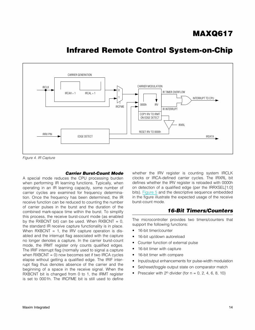
Figure 4. IR Capture . . . . . . . . . . . . . . . . . . . . . . . . . . . . . . . . . . . . . . . . . . . . . . . . . . . . . . . . . . . . . . . . . . . . . . . . . . . 14
Figure 5. Receive Burst-Count Example . . . . . . . . . . . . . . . . . . . . . . . . . . . . . . . . . . . . . . . . . . . . . . . . . . . . . . . . . . . 15
Figure 6. Power-Fail Detection During Normal Operation . . . . . . . . . . . . . . . . . . . . . . . . . . . . . . . . . . . . . . . . . . . . . . 17
Figure 7. Stop Mode Power-Fail Detection States with Power-Fail Monitor Enabled . . . . . . . . . . . . . . . . . . . . . . . . . . 19
Figure 8. Stop Mode Power-Fail Detection with Power-Fail Monitor Disabled . . . . . . . . . . . . . . . . . . . . . . . . . . . . . . . 20
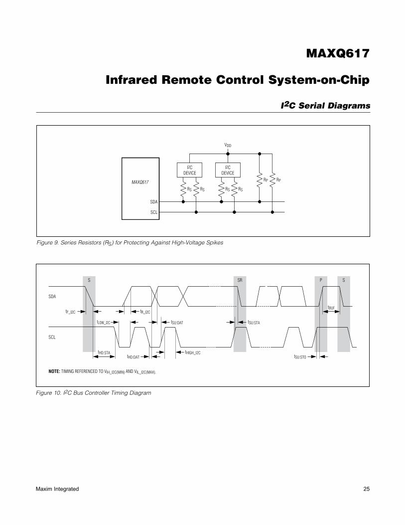
Figure 9. Series Resistors (RS) for Protecting Against High-Voltage Spikes . . . . . . . . . . . . . . . . . . . . . . . . . . . . . . . . 25
Figure 10. I2C Bus Controller Timing Diagram. . . . . . . . . . . . . . . . . . . . . . . . . . . . . . . . . . . . . . . . . . . . . . . . . . . . . . . 25
Figure 11. SPI Master Communication Timing . . . . . . . . . . . . . . . . . . . . . . . . . . . . . . . . . . . . . . . . . . . . . . . . . . . . . . . 27
Figure 12. SPI Slave Communication Timing . . . . . . . . . . . . . . . . . . . . . . . . . . . . . . . . . . . . . . . . . . . . . . . . . . . . . . . . 27
Figure 13. USART Timing Diagram . . . . . . . . . . . . . . . . . . . . . . . . . . . . . . . . . . . . . . . . . . . . . . . . . . . . . . . . . . . . . . . 28
Table 1. Watchdog Interrupt Timeout (Sysclk = 12MHz, CD[1:0] = 00). . . . . . . . . . . . . . . . . . . . . . . . . . . . . . . . . . . . 10
Table 2. USART Mode Details . . . . . . . . . . . . . . . . . . . . . . . . . . . . . . . . . . . . . . . . . . . . . . . . . . . . . . . . . . . . . . . . . . . 16
Table 3. Power-Fail Warning Voltage Selection . . . . . . . . . . . . . . . . . . . . . . . . . . . . . . . . . . . . . . . . . . . . . . . . . . . . . . 17
Table 4. Power-Fail Detection States During Normal Operation . . . . . . . . . . . . . . . . . . . . . . . . . . . . . . . . . . . . . . . . . 18
Table 5. Stop Mode Power-Fail Detection States with Power-Fail Monitor Enabled . . . . . . . . . . . . . . . . . . . . . . . . . . 19
Table 6. Stop Mode Power-Fail Detection States with Power-Fail Monitor Disabled . . . . . . . . . . . . . . . . . . . . . . . . . . 20
Appendix A. . . . . . . . . . . . . . . . . . . . . . . . . . . . . . . . . . . . . . . . . . . . . . . . . . . . . . . . . . . . . . . . . . . . . . . . . . . . . . . . . . 23
I2C Serial peripheral specifications . . . . . . . . . . . . . . . . . . . . . . . . . . . . . . . . . . . . . . . . . . . . . . . . . . . . . . . . . . . . . . . 23
I2C Serial Diagrams . . . . . . . . . . . . . . . . . . . . . . . . . . . . . . . . . . . . . . . . . . . . . . . . . . . . . . . . . . . . . . . . . . . . . . . . . . . 25
SPI Electrical Characteristics . . . . . . . . . . . . . . . . . . . . . . . . . . . . . . . . . . . . . . . . . . . . . . . . . . . . . . . . . . . . . . . . . . . . 26
SPI Timing Diagrams . . . . . . . . . . . . . . . . . . . . . . . . . . . . . . . . . . . . . . . . . . . . . . . . . . . . . . . . . . . . . . . . . . . . . . . . . . 27
USART Timing . . . . . . . . . . . . . . . . . . . . . . . . . . . . . . . . . . . . . . . . . . . . . . . . . . . . . . . . . . . . . . . . . . . . . . . . . . . . . . . 28
Revision History . . . . . . . . . . . . . . . . . . . . . . . . . . . . . . . . . . . . . . . . . . . . . . . . . . . . . . . . . . . . . . . . . . . . . . . . . . . . . . 29
MAXQ617
Infrared Remote Control System-on-Chip
4Maxim Integrated
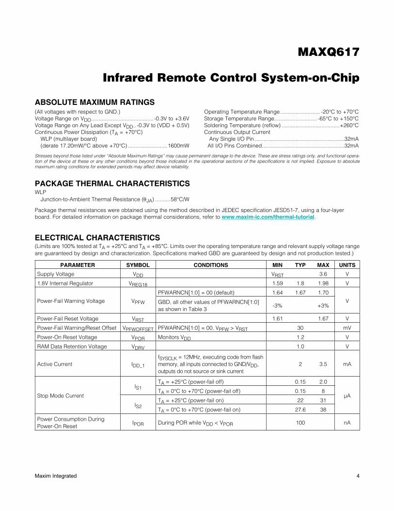
(All voltages with respect to GND.)Voltage Range on VDD .........................................-0.3V to +3.6VVoltage Range on Any Lead Except VDD .. -0.3V to (VDD + 0.5V)Continuous Power Dissipation (TA = +70NC)
WLP (multilayer board) (derate 17.20mW/NC above +70NC) ..........................1600mW
Operating Temperature Range .......................... -20NC to +70NCStorage Temperature Range ............................ -65NC to +150NCSoldering Temperature (reflow) ......................................+260NCContinuous Output Current Any Single I/O Pin ...........................................................32mA All I/O Pins Combined ......................................................32mA
ABSOLUTE MAXIMUM RATINGS
Stresses beyond those listed under “Absolute Maximum Ratings” may cause permanent damage to the device. These are stress ratings only, and functional opera-tion of the device at these or any other conditions beyond those indicated in the operational sections of the specifications is not implied. Exposure to absolute maximum rating conditions for extended periods may affect device reliability.
ELECTRICAL CHARACTERISTICS(Limits are 100% tested at TA = +25°C and TA = +85°C. Limits over the operating temperature range and relevant supply voltage range are guaranteed by design and characterization. Specifications marked GBD are guaranteed by design and not production tested.)
WLP Junction-to-Ambient Thermal Resistance (qJA) ..........58°C/W
Package thermal resistances were obtained using the method described in JEDEC specification JESD51-7, using a four-layer board. For detailed information on package thermal considerations, refer to www.maxim-ic.com/thermal-tutorial.
PACKAGE THERMAL CHARACTERISTICS
PARAMETER SYMBOL CONDITIONS MIN TYP MAX UNITS
Supply Voltage VDD VRST 3.6 V
1.8V Internal Regulator VREG18 1.59 1.8 1.98 V
Power-Fail Warning Voltage VPFW
PFWARNCN[1:0] = 00 (default) 1.64 1.67 1.70
VGBD, all other values of PFWARNCN[1:0] as shown in Table 3
-3% +3%
Power-Fail Reset Voltage VRST 1.61 1.67 V
Power-Fail Warning/Reset Offset VPFWOFFSET PFWARNCN[1:0] = 00, VPFW > VRST 30 mV
Power-On Reset Voltage VPOR Monitors VDD 1.2 V
RAM Data Retention Voltage VDRV 1.0 V
Active Current IDD_1
fSYSCLK = 12MHz, executing code from flash memory, all inputs connected to GND/VDD, outputs do not source or sink current
2 3.5 mA
Stop Mode Current
IS1 TA = +25NC (power-fail off) 0.15 2.0
FATA = 0NC to +70NC (power-fail off) 0.15 8
IS2TA = +25NC (power-fail on) 22 31
TA = 0NC to +70NC (power-fail on) 27.6 38
Power Consumption During Power-On Reset
IPOR During POR while VDD < VPOR 100 nA
MAXQ617
Infrared Remote Control System-on-Chip
5Maxim Integrated
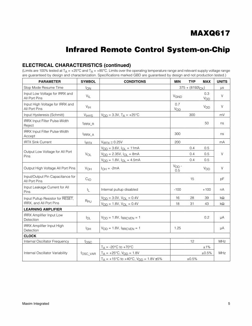
ELECTRICAL CHARACTERISTICS (continued)(Limits are 100% tested at TA = +25°C and TA = +85°C. Limits over the operating temperature range and relevant supply voltage range are guaranteed by design and characterization. Specifications marked GBD are guaranteed by design and not production tested.)
PARAMETER SYMBOL CONDITIONS MIN TYP MAX UNITS
Stop Mode Resume Time tON 375 + (8192tCK) Fs
Input Low Voltage for IRRX and All Port Pins
VIL VGND0.3 VDD
V
Input High Voltage for IRRX and All Port Pins
VIH0.7 VDD
VDD V
Input Hysteresis (Schmitt) VIHYS VDD = 3.3V, TA = +25NC 300 mV
IRRX Input Filter Pulse-Width Reject
tIRRX_R 50 ns
IRRX Input Filter Pulse-Width Accept
tIRRX_A 300 ns
IRTX Sink Current IIRTX VIRTX ≥ 0.25V 200 mA
Output Low Voltage for All Port Pins
VOL
VDD = 3.6V, IOL = 11mA 0.4 0.5
VVDD = 2.35V, IOL = 8mA 0.4 0.5
VDD = 1.8V, IOL = 4.5mA 0.4 0.5
Output High Voltage All Port Pins VOH IOH = -2mAVDD - 0.5
VDD V
Input/Output Pin Capacitance for All Port Pins
CIO 15 pF
Input Leakage Current for All Pins
IL Internal pullup disabled -100 +100 nA
Input Pullup Resistor for RESET, IRRX, and All Port Pins
RPUVDD = 3.0V, VOL = 0.4V 16 28 39 kI
VDD = 1.8V, VOL = 0.4V 18 31 43 kI
LEARNING AMPLIFIER
IRRX Amplifier Input Low Detection
IDL VDD = 1.8V, IRRCVEN = 1 0.2 FA
IRRX Amplifier Input High Detection
IDH VDD = 1.8V, IRRCVEN = 1 1.25 FA
CLOCK
Internal Oscillator Frequency fOSC 12 MHz
Internal Oscillator Variability fOSC_VAR
TA = -20NC to +70NC ±1%
MHzTA = +25NC, VDD = 1.8V ±0.5%
TA = +15NC to +40NC, VDD = 1.8V ±5% ±0.5%
MAXQ617
Infrared Remote Control System-on-Chip
6Maxim Integrated
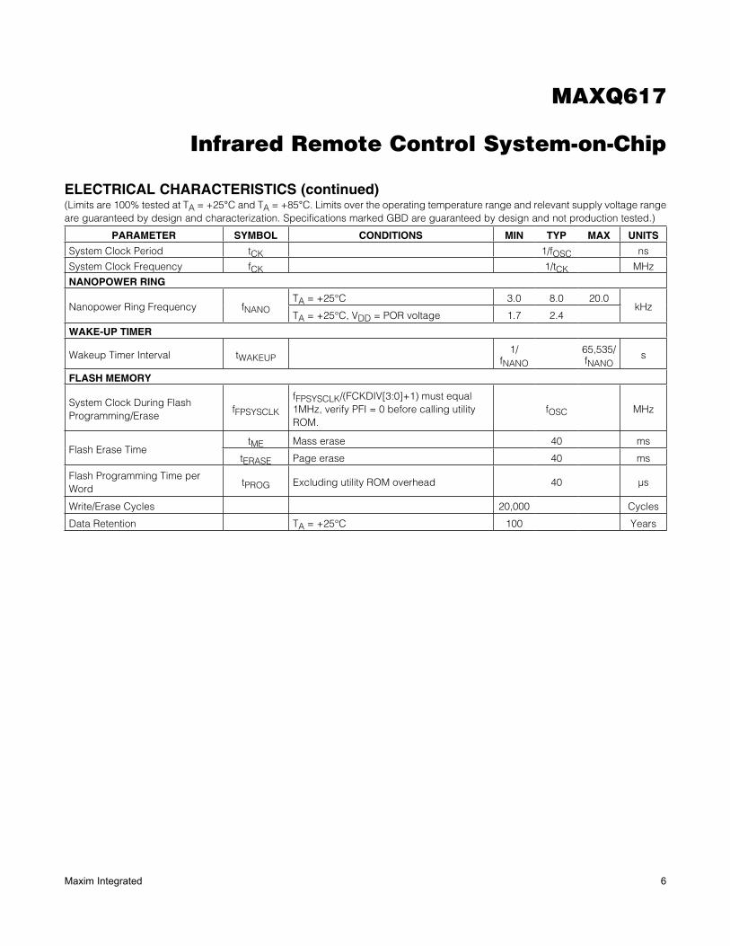
ELECTRICAL CHARACTERISTICS (continued)(Limits are 100% tested at TA = +25°C and TA = +85°C. Limits over the operating temperature range and relevant supply voltage range are guaranteed by design and characterization. Specifications marked GBD are guaranteed by design and not production tested.)
PARAMETER SYMBOL CONDITIONS MIN TYP MAX UNITS
System Clock Period tCK 1/fOSC ns
System Clock Frequency fCK 1/tCK MHz
NANOPOWER RING
Nanopower Ring Frequency fNANOTA = +25NC 3.0 8.0 20.0
kHzTA = +25NC, VDD = POR voltage 1.7 2.4
WAKE-UP TIMER
Wakeup Timer Interval tWAKEUP1/
fNANO
65,535/ fNANO
s
FLASH MEMORY
System Clock During Flash Programming/Erase
fFPSYSCLK
fFPSYSCLK/(FCKDIV[3:0]+1) must equal 1MHz, verify PFI = 0 before calling utility ROM.
fOSC MHz
Flash Erase TimetME Mass erase 40 ms
tERASE Page erase 40 ms
Flash Programming Time per Word
tPROG Excluding utility ROM overhead 40 Fs
Write/Erase Cycles 20,000 Cycles
Data Retention TA = +25NC 100 Years
MAXQ617
Infrared Remote Control System-on-Chip
7Maxim Integrated
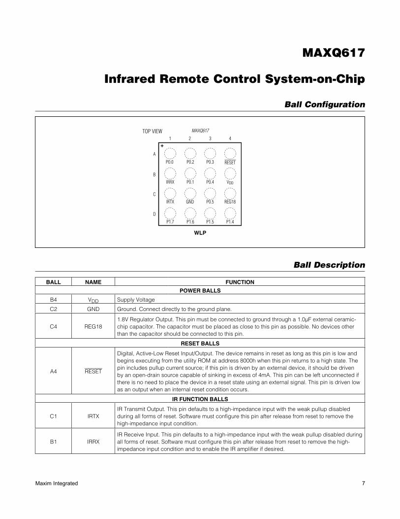
Ball Configuration
Ball Description
BALL NAME FUNCTION
POWER BALLS
B4 VDD Supply Voltage
C2 GND Ground. Connect directly to the ground plane.
C4 REG181.8V Regulator Output. This pin must be connected to ground through a 1.0FF external ceramic-chip capacitor. The capacitor must be placed as close to this pin as possible. No devices other than the capacitor should be connected to this pin.
RESET BALLS
A4 RESET
Digital, Active-Low Reset Input/Output. The device remains in reset as long as this pin is low and begins executing from the utility ROM at address 8000h when this pin returns to a high state. The pin includes pullup current source; if this pin is driven by an external device, it should be driven by an open-drain source capable of sinking in excess of 4mA. This pin can be left unconnected if there is no need to place the device in a reset state using an external signal. This pin is driven low as an output when an internal reset condition occurs.
IR FUNCTION BALLS
C1 IRTXIR Transmit Output. This pin defaults to a high-impedance input with the weak pullup disabled during all forms of reset. Software must configure this pin after release from reset to remove the high-impedance input condition.
B1 IRRXIR Receive Input. This pin defaults to a high-impedance input with the weak pullup disabled during all forms of reset. Software must configure this pin after release from reset to remove the high-impedance input condition and to enable the IR amplifier if desired.
WLP
TOP VIEW
REG18IRTX
VDDIRRX
RESETP0.0
MAXQ617
+1 2 3 4
A
GND P0.5
P0.1 P0.4
P1.4P1.7 P1.6 P1.5
P0.2 P0.3
B
C
D
MAXQ617
Infrared Remote Control System-on-Chip
8Maxim Integrated
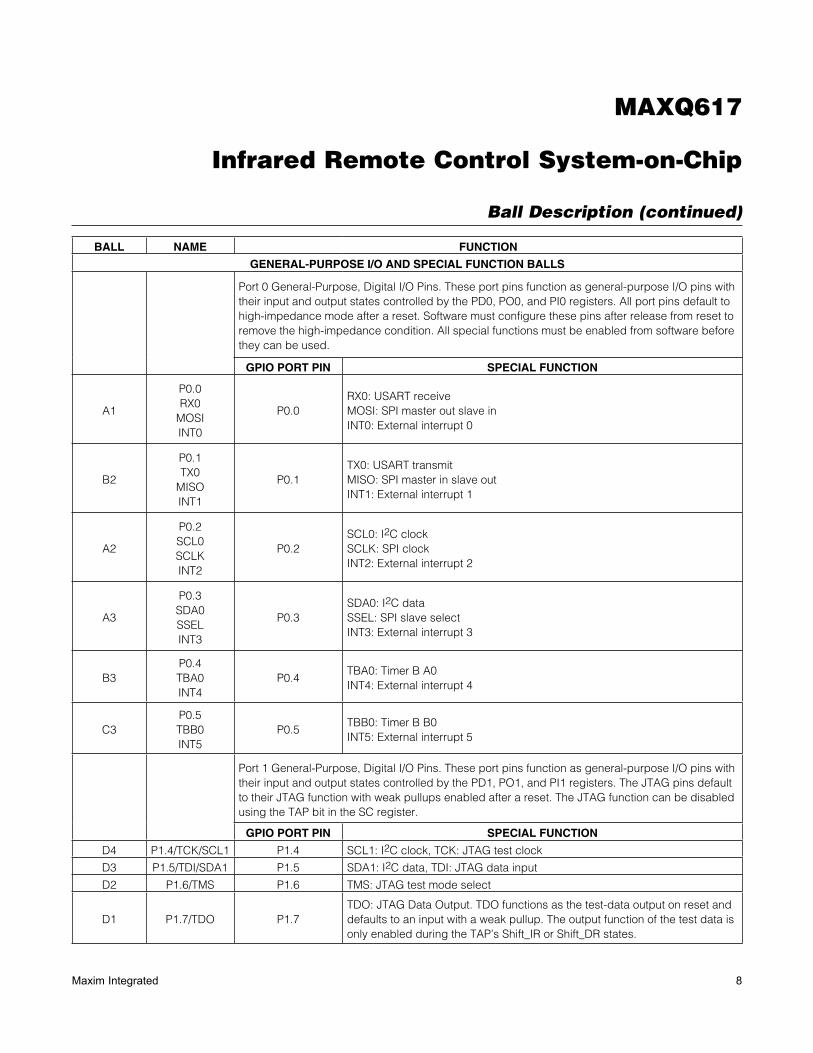
Ball Description (continued)
BALL NAME FUNCTION
GENERAL-PURPOSE I/O AND SPECIAL FUNCTION BALLS
Port 0 General-Purpose, Digital I/O Pins. These port pins function as general-purpose I/O pins with their input and output states controlled by the PD0, PO0, and PI0 registers. All port pins default to high-impedance mode after a reset. Software must configure these pins after release from reset to remove the high-impedance condition. All special functions must be enabled from software before they can be used.
GPIO PORT PIN SPECIAL FUNCTION
A1
P0.0RX0
MOSIINT0
P0.0RX0: USART receiveMOSI: SPI master out slave inINT0: External interrupt 0
B2
P0.1TX0
MISOINT1
P0.1TX0: USART transmitMISO: SPI master in slave outINT1: External interrupt 1
A2
P0.2SCL0SCLKINT2
P0.2SCL0: I2C clockSCLK: SPI clockINT2: External interrupt 2
A3
P0.3SDA0SSELINT3
P0.3SDA0: I2C dataSSEL: SPI slave selectINT3: External interrupt 3
B3P0.4TBA0INT4
P0.4TBA0: Timer B A0INT4: External interrupt 4
C3P0.5TBB0INT5
P0.5TBB0: Timer B B0INT5: External interrupt 5
Port 1 General-Purpose, Digital I/O Pins. These port pins function as general-purpose I/O pins with their input and output states controlled by the PD1, PO1, and PI1 registers. The JTAG pins default to their JTAG function with weak pullups enabled after a reset. The JTAG function can be disabled using the TAP bit in the SC register.
GPIO PORT PIN SPECIAL FUNCTION
D4 P1.4/TCK/SCL1 P1.4 SCL1: I2C clock, TCK: JTAG test clock
D3 P1.5/TDI/SDA1 P1.5 SDA1: I2C data, TDI: JTAG data input
D2 P1.6/TMS P1.6 TMS: JTAG test mode select
D1 P1.7/TDO P1.7TDO: JTAG Data Output. TDO functions as the test-data output on reset and defaults to an input with a weak pullup. The output function of the test data is only enabled during the TAP’s Shift_IR or Shift_DR states.
MAXQ617
Infrared Remote Control System-on-Chip
9Maxim Integrated
Detailed Description
The MAXQ617 provides integrated, low-cost solutions that simplify the design of IR communications equipment such as universal remote controls. Standard features include the highly optimized, single-cycle, MAXQ, 16-bit RISC core; 80KB flash memory; 4KB data RAM; soft stack; 16 general-purpose registers; and three data pointers. The MAXQ core has the industry’s best MIPS/mA rating, allowing developers to achieve the same per-formance as competing microcontrollers at substantially lower clock rates. Lower active-mode current combined with the even lower stop-mode current (0.2FA typ) results in increased battery life. Application-specific peripherals include flexible timers for generating IR carrier frequen-cies and modulation. A high-current IR drive pin oper-ates with an internal receiver amplifier without external components. It also includes general-purpose I/O pins ideal for keypad matrix input, and a power-fail-detection circuit to notify the application when the supply voltage is nearing the microcontroller’s minimum operating voltage.
The internal 12MHz oscillator requires no external com-ponents and executes instructions. Operating from DC to 12MHz, almost all instructions execute in a single clock cycle (83.3ns at 12MHz), enabling nearly 12MIPS true-code operation. When active device operation is not required, an ultra-low-power stop mode can be invoked from software, resulting in quiescent current consump-tion of less than 0.2FA (typ) and 2.0FA (max). The com-bination of high-performance instructions and ultra-low stop-mode current increases battery life over competing microcontrollers. An integrated POR circuit with brownout support resets the device to a known condition following a power-up cycle or brownout condition. Additionally, a power-fail warning flag is set, and a power-fail interrupt can be generated when the system voltage falls below the power-fail warning voltage, VPFW. The configurable power-fail warning feature allows the application to notify the user that the system supply is low and appropriate action should be taken.
Microprocessor
The device is based on Maxim Integrated’s low-pow-er, 16-bit MAXQ20S. The core supports the Harvard memory architecture with separate 16-bit program and data address buses. A fixed 16-bit instruction word is standard, but data can be arranged in 8 or 16 bits. The MAXQ core in the device is implemented as a pipe-
lined processor with performance approaching 1MIPS per MHz. The 16-bit data path is implemented around register modules, and each register module contributes specific functions to the core. The accumulator module consists of sixteen 16-bit registers and is tightly coupled with the arithmetic logic unit (ALU). A configurable soft stack supports program flow.
Execution of instructions is triggered by data trans-fer between functional register modules or between a functional register module and memory. Because data movement involves only source and destination modules, circuit switching activities are limited to active modules only. For power-conscious applications, this approach localizes power dissipation and minimizes switching noise. The modular architecture also provides a maxi-mum of flexibility and reusability that are important for a microprocessor used in embedded applications.
The MAXQ instruction set is highly orthogonal. All arith-metical and logical operations can use any register in conjunction with the accumulator. Data movement is sup-ported from any register to any other register. Memory is accessed through specific data-pointer registers with autoincrement/decrement support.
Memory
The microcontroller incorporates several memory types:
• 80KB flash memory
• 4KB SRAM data memory
• Dedicated utility ROM
• Soft stack
Stack MemoryThe device provides a soft stack that can be used to store program return addresses (for subroutine calls and interrupt handling) and other general-purpose data. This soft stack is located in the SRAM data memory, which means that the SRAM data memory must be shared between the soft stack and general-purpose application data storage. However, the location and size of the soft stack is determined by the user, providing maximum flexibility when allocating resources for a particular appli-cation. The stack is used automatically by the processor when the CALL, RET, and RETI instructions are executed and when an interrupt is serviced. An application can also store and retrieve values explicitly using the stack by means of the PUSH, POP, and POPI instructions.
MAXQ617
Infrared Remote Control System-on-Chip
10Maxim Integrated
The SP pointer indicates the current top of the stack, which initializes by default to the top of the SRAM data memory. As values are pushed onto the stack, the SP pointer decrements, which means that the stack grows downward towards the bottom (lowest address) of the data memory. Popping values off the stack causes the SP pointer value to increase. Refer to the User’s Guide for more details.
Utility ROMThe utility ROM is located in program space beginning at address 8000h. This ROM includes the following routines:
• Production test routines (internal memory tests, mem-ory loader, etc.), which are used for internal testing only, and are generally of no use to the end-applica-tion developer
• User-callable routines for buffer copying and fast table lookup (more information on these routines can be found in the User’s Guide)
Following any reset, execution begins in the utility ROM at address 8000h. At this point, unless test mode has been invoked (which requires special programming through the JTAG interface), the utility ROM in the device always automatically jumps to location 0000h, which is the beginning of user application code.
Watchdog Timer
The internal watchdog timer greatly increases system reli-ability. The timer resets the device if software execution is disturbed. The watchdog timer is a free-running coun-ter designed to be periodically reset by the application software. If software is operating correctly, the counter is
periodically reset and never reaches its maximum count. However, if software operation is interrupted, the timer does not reset, triggering a system reset and option-ally a watchdog timer interrupt. This protects the system against electrical noise or electrostatic discharge (ESD) upsets that could cause uncontrolled processor opera-tion. The internal watchdog timer is an upgrade to older designs with external watchdog devices, reducing sys-tem cost and simultaneously increasing reliability.
The watchdog timer functions as the source of both the watchdog timer timeout and the watchdog timer reset. The timeout period can be programmed in a range of 215 to 224 system clock cycles. An interrupt is gener-ated when the timeout period expires if the interrupt is enabled. All watchdog timer resets follow the pro-grammed interrupt timeouts by 512 system clock cycles. If the watchdog timer is not restarted for another full interval in this time period, a system reset occurs when the reset timeout expires. See Table 1.
IR Carrier Generation and Modulation Timer
The dedicated IR timer/counter module simplifies low-speed infrared (IR) communication. The IR timer imple-ments two pins (IRTX and IRRX) for supporting IR trans-mit and receive, respectively. The IRTX pin has no corre-sponding port pin designation, so the standard PD, PO, and PI port control status bits are not present. However, the IRTX pin output can be manipulated high or low using the PWCN.IRTXOUT and PWCN.IRTXOE bits when the IR timer is not enabled (i.e., IREN = 0).
Table 1. Watchdog Interrupt Timeout (Sysclk = 12MHz, CD[1:0] = 00)
WD[1:0] WATCHDOG CLOCK WATCHDOG INTERRUPT TIMEOUTWATCHDOG RESET AFTER
WATCHDOG INTERRUPT (µs)
00 Sysclk/215 2.7ms 42.7
01 Sysclk/218 21.9ms 42.7
10 Sysclk/221 174.7ms 42.7
11 Sysclk/224 1.4s 42.7

MAXQ617
Infrared Remote Control System-on-Chip
11Maxim Integrated
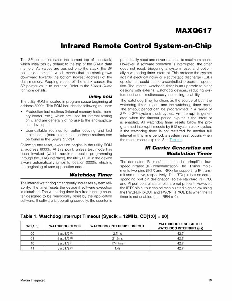
The IR timer is composed of a carrier generator and a carrier modulator. The carrier generation module uses the 16-bit IR carrier register (IRCA) to define the high and low time of the carrier through the IR carrier high byte (IRCAH) and IR carrier low byte (IRCAL). The carrier modulator uses the IR data bit (IRDATA) and IR modula-tor time register (IRMT) to determine whether the carrier or the idle condition is present on IRTX.
The IR timer is enabled when the IR enable bit (IREN) is set to 1. The IR Value register (IRV) defines the begin-ning value for the carrier modulator. During transmission, the IRV register is initially loaded with the IRMT value and begins down counting towards 0000h, whereas in receive mode it counts upward from the initial IRV regis-ter value. During the receive operation, the IRV register can be configured to reload with 0000h when capture occurs on detection of selected edges or can be allowed to continue free-running throughout the receive opera-tion. An overflow occurs when the IR timer value rolls over from 0FFFFh to 0000h. The IR overflow flag (IROV) is set to 1 and an interrupt is generated if enabled (IRIE = 1).
Carrier Generation ModuleThe IRCAH byte defines the carrier high time in terms of the number of IR input clocks, whereas the IRCAL byte defines the carrier low time.
• IR Input Clock (fIRCLK) = fSYS/2IRDIV[2:0]
• Carrier Frequency (fCARRIER) = fIRCLK/(IRCAH + IRCAL + 2)
• Carrier High Time = IRCAH + 1
• Carrier Low Time = IRCAL + 1
• Carrier Duty Cycle = (IRCAH + 1)/(IRCAH + IRCAL + 2)
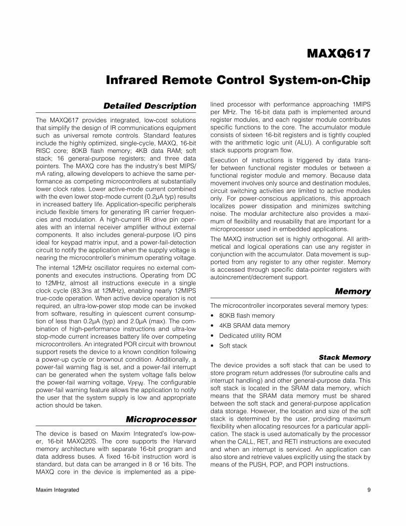
During transmission, the IRCA register is latched for each IRV down-count interval, and is sampled along with the IRTXPOL and IRDATA bits at the beginning of each new IRV down-count interval so that duty-cycle variation and frequency shifting is possible from one interval to the next, which is illustrated in Figure 1.
Figure 2 illustrates the basic carrier generation and its path to the IRTX output pin. The IR transmit polarity bit (IRTXPOL) defines the starting/idle state and the carrier polarity of the IRTX pin when the IR timer is enabled.
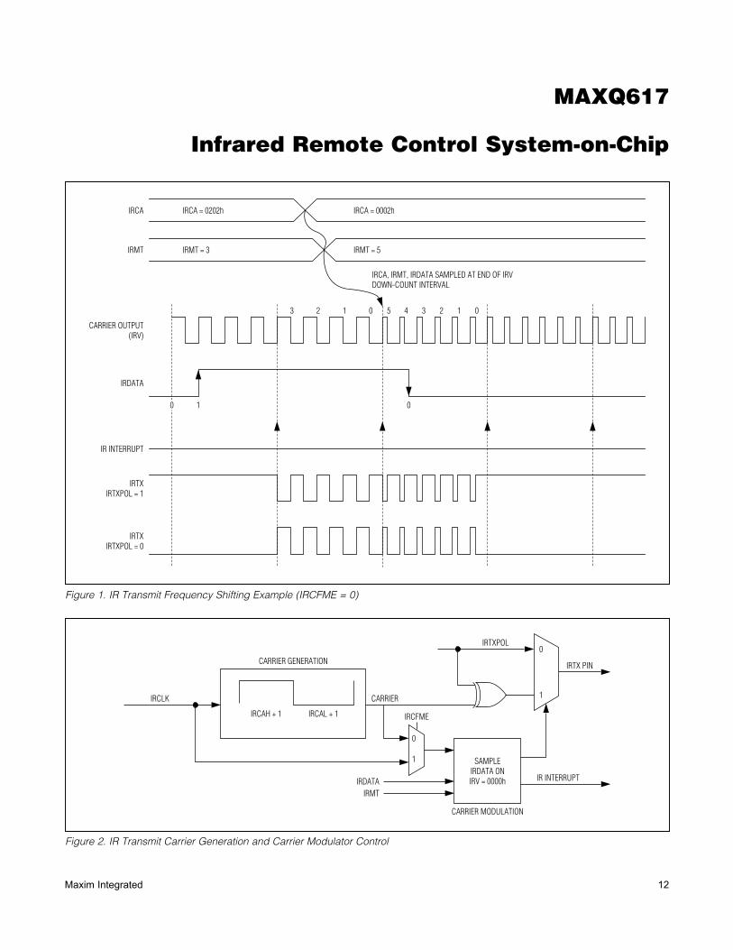
IR TransmissionDuring IR transmission (IRMODE = 1), the carrier genera-tor creates the appropriate carrier waveform, while the carrier modulator performs the modulation. The carrier modulation can be performed as a function of carrier cycles or IRCLK cycles dependent on the setting of the IRCFME bit. When IRCFME = 0, the IRV down counter is clocked by the carrier frequency and thus the modulation is a function of carrier cycles (Figure 3). When IRCFME = 1, the IRV down counter is clocked by IRCLK, allowing carrier modulation timing with IRCLK resolution.
The IRTXPOL bit defines the starting/idle state as well as the carrier polarity for the IRTX pin. If IRTXPOL = 1, the IRTX pin is set to a logic-high when the IR timer module is enabled. If IRTXPOL = 0, the IRTX pin is set to a logic-low when the IR timer is enabled.
A separate register bit, IR data (IRDATA), is used to determine whether the carrier generator output is output to the IRTX pin for the next IRMT carrier cycles. When IRDATA = 1, the car-rier waveform (or inversion of this waveform if IRTXPOL = 1) is output on the IRTX pin during the next IRMT cycles. When IRDATA = 0, the idle condition, as defined by IRTXPOL, is output on the IRTX pin during the next IRMT cycles.
The IR timer acts as a down counter in transmit mode. An IR transmission starts when the IREN bit is set to 1 when IRMODE = 1; when the IRMODE bit is set to 1 when IREN = 1; or when IREN and IRMODE are both set to 1 in the same instruction. The IRMT and IRCA registers, along with the IRDATA and IRTXPOL bits, are sampled at the beginning of the transmit process and every time the IR timer value reload its value. When the IRV reaches 0000h value, on the next carrier clock, it does the following:
1) Reloads IRV with IRMT.
2) Samples IRCA, IRDATA, and IRTXPOL.
3) Generates IRTX accordingly.
4) Sets IRIF to 1.
5) Generates an interrupt to the CPU if enabled (IRIE = 1).
To terminate the current transmission, the user can switch to receive mode (IRMODE = 0) or clear IREN to 0.
Carrier Modulation Time = IRMT + 1 carrier cycles
MAXQ617
Infrared Remote Control System-on-Chip
12Maxim Integrated
Figure 1. IR Transmit Frequency Shifting Example (IRCFME = 0)
Figure 2. IR Transmit Carrier Generation and Carrier Modulator Control
1
0
0
1 SAMPLEIRDATA ONIRV = 0000h
CARRIER MODULATION
CARRIER GENERATION
CARRIERIRCLK
IRCFMEIRCAL + 1IRCAH + 1
IRDATAIRMT
IRTXPOL
IRTX PIN
IR INTERRUPT
CARRIER OUTPUT(IRV)
IRDATA
IR INTERRUPT
01
IRMT = 3
0
IRTXIRTXPOL = 1
IRTXIRTXPOL = 0
IRCA
IRMT IRMT = 5
IRCA = 0202h IRCA = 0002h
IRCA, IRMT, IRDATA SAMPLED AT END OF IRVDOWN-COUNT INTERVAL
3 12 0 5 4 3 2 1 0
MAXQ617
Infrared Remote Control System-on-Chip
13Maxim Integrated
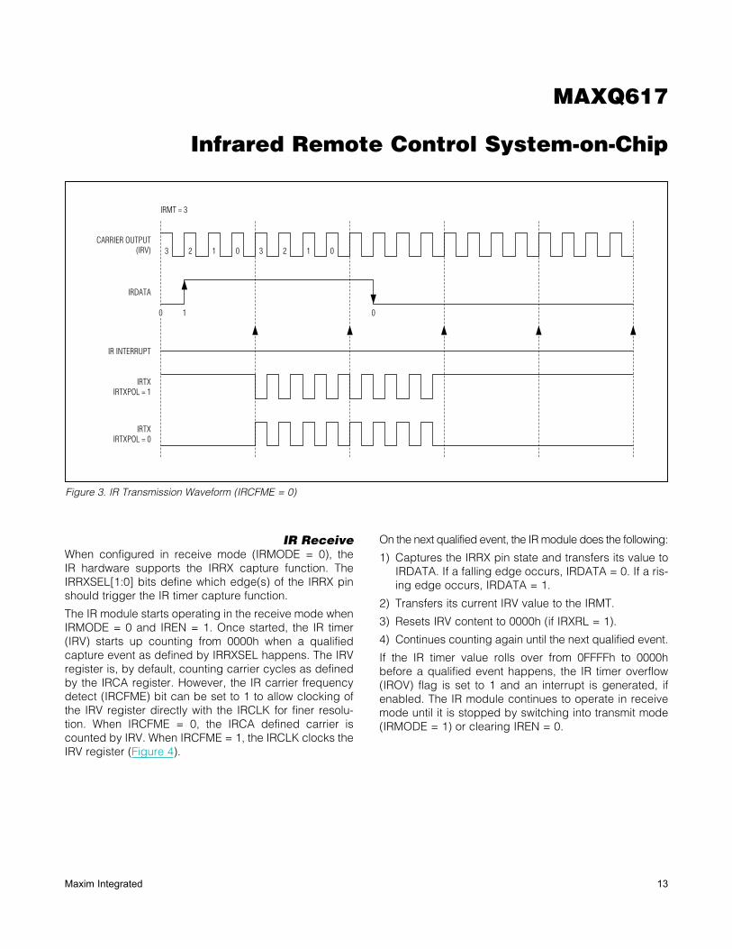
IR ReceiveWhen configured in receive mode (IRMODE = 0), the IR hardware supports the IRRX capture function. The IRRXSEL[1:0] bits define which edge(s) of the IRRX pin should trigger the IR timer capture function.
The IR module starts operating in the receive mode when IRMODE = 0 and IREN = 1. Once started, the IR timer (IRV) starts up counting from 0000h when a qualified capture event as defined by IRRXSEL happens. The IRV register is, by default, counting carrier cycles as defined by the IRCA register. However, the IR carrier frequency detect (IRCFME) bit can be set to 1 to allow clocking of the IRV register directly with the IRCLK for finer resolu-tion. When IRCFME = 0, the IRCA defined carrier is counted by IRV. When IRCFME = 1, the IRCLK clocks the IRV register (Figure 4).
On the next qualified event, the IR module does the following:
1) Captures the IRRX pin state and transfers its value to IRDATA. If a falling edge occurs, IRDATA = 0. If a ris-ing edge occurs, IRDATA = 1.
2) Transfers its current IRV value to the IRMT.
3) Resets IRV content to 0000h (if IRXRL = 1).
4) Continues counting again until the next qualified event.
If the IR timer value rolls over from 0FFFFh to 0000h before a qualified event happens, the IR timer overflow (IROV) flag is set to 1 and an interrupt is generated, if enabled. The IR module continues to operate in receive mode until it is stopped by switching into transmit mode (IRMODE = 1) or clearing IREN = 0.
Figure 3. IR Transmission Waveform (IRCFME = 0)
CARRIER OUTPUT(IRV)
IRDATA
IR INTERRUPT
IRTXIRTXPOL = 1
IRTXIRTXPOL = 0
010
IRMT = 3
23 1 0 23 1 0
MAXQ617
Infrared Remote Control System-on-Chip
14Maxim Integrated
Carrier Burst-Count ModeA special mode reduces the CPU processing burden when performing IR learning functions. Typically, when operating in an IR learning capacity, some number of carrier cycles are examined for frequency determina-tion. Once the frequency has been determined, the IR receive function can be reduced to counting the number of carrier pulses in the burst and the duration of the combined mark-space time within the burst. To simplify this process, the receive burst-count mode (as enabled by the RXBCNT bit) can be used. When RXBCNT = 0, the standard IR receive capture functionality is in place. When RXBCNT = 1, the IRV capture operation is dis-abled and the interrupt flag associated with the capture no longer denotes a capture. In the carrier burst-count mode, the IRMT register only counts qualified edges. The IRIF interrupt flag (normally used to signal a capture when RXBCNT = 0) now becomes set if two IRCA cycles elapse without getting a qualified edge. The IRIF inter-rupt flag thus denotes absence of the carrier and the beginning of a space in the receive signal. When the RXBCNT bit is changed from 0 to 1, the IRMT register is set to 0001h. The IRCFME bit is still used to define
whether the IRV register is counting system IRCLK clocks or IRCA-defined carrier cycles. The IRXRL bit defines whether the IRV register is reloaded with 0000h on detection of a qualified edge (per the IRRXSEL[1:0] bits). Figure 5 and the descriptive sequence embedded in the figure illustrate the expected usage of the receive burst-count mode.
16-Bit Timers/Counters
The microcontroller provides two timers/counters that support the following functions:
• 16-bit timer/counter
• 16-bit up/down autoreload
• Counter function of external pulse
• 16-bit timer with capture
• 16-bit timer with compare
• Input/output enhancements for pulse-width modulation
• Set/reset/toggle output state on comparator match
• Prescaler with 2n divider (for n = 0, 2, 4, 6, 8, 10)
Figure 4. IR Capture
0
1
0000h IRV
CARRIER MODULATION
CARRIER GENERATION
IRCLK
IRCFME
IRCAL + 1IRCAH + 1
INTERRUPT TO CPU
IRDATAIRRX PIN
RESET IRV TO 0000h
IR TIMER OVERFLOW
IR INTERRUPT
IRXRL
COPY IRV TO IRMTON EDGE DETECT
EDGE DETECT

MAXQ617
Infrared Remote Control System-on-Chip
15Maxim Integrated
Serial Peripherals
Serial Peripheral Interface (SPI)The device provides two SPI ports. The SPI is an inter-device bus protocol that provides fast, synchronous, full-duplex communications between devices. The integrated SPI interface acts as either an SPI master or slave device. The master drives the synchronous clock and selects which of several slaves is being addressed. Every SPI peripheral consists of a single shift register and control circuitry so that an addressed serial peripheral interface SPI peripheral is simultaneously transmitting and receiv-ing. The maximum SPI master transfer rate is Sysclk/2.
When operating as an SPI slave, the device can support up to Sysclk/4 SPI transfer rate. Data can be transferred as an 8-bit or 16-bit value, MSB first. In addition, the SPI module supports configuration of the active SSEL state through the slave active-select pin.
Four signals are used in SPI communication:
• SCLK: The synchronous clock used by all devices. The master drives this clock and the slaves receive the clock. Note that SCLK can be gated and need not be driven between SPI transactions.
• MOSI: Master out-slave in. This is the main data line driven by the master to all slaves on the SPI bus. Only the selected slave clocks data from MOSI.
Figure 5. Receive Burst-Count Example
1
1 4
5
6
7
8
9
TO
2 3 4 6 7
5
8
9
CARRIER FREQUENCYCALCULATION
IRRX
IRV
IRMT
IRMT = PULSE COUNTING IRMT = PULSE COUNTINGIRV = CARRIER CYCLE COUNTING
CAPTURE INTERRUPT (IRIF = 1).IRV ≥ IRMT.IRV = 0 (IF IRXRL = 1).
SOFTWARE SETS IRCA = CARRIER FREQUENCY.SOFTWARE SETS RXBCNT = 1 (WHICH CLEARS IRMT = 0001 IN HARDWARE).SOFTWARE CLEARS IRCFME = 0 SO THAT IRV COUNTS CARRIER CYCLES. IRV IS RESET TO 0 ON QUALIFIED EDGE DETECTION IF IRXRL = 1.SOFTWARE ADDS TO IRMT THE NUMBER OF PULSES USED FOR CARRIER MEASUREMENT.IRCA x 2x COUNTER FOR SPACE CAN BEGIN IMMEDIATELY (QUALIFIED EDGE RESETS).
QUALIFIED EDGE DETECTED: IRMT++IRV RESET TO 0 IF IRXRL = 1.
IRCA x 2 PERIOD ELAPSES: IRIF = 1; CARRIER ABSENCE = SPACE.BURST MARK = IRMT PULSES.SOFTWARE CLEARS RXBCNT = 0 SO THAT WE CAPTURE ON THE NEXT QUALIFIED EDGE.
QUALIFIED EDGE DETECTED: IRIF = 1, CAPTURE IRV IRMT AS THE BURST SPACE (PLUS UP TO ONE CARRIER CYCLE).
SOFTWARE SET RXBCNT = 1 AS IN (5).CONTINUE (5) TO (8) UNTIL LEARNING SPACE EXCEEDS SOME DURATION. IRV ROLLOVERS CAN BE USED.
MAXQ617
Infrared Remote Control System-on-Chip
16Maxim Integrated
• MISO: Master in-slave out. This is the main data line driven by the selected slave to the master. Only the selected slave may drive this circuit. In fact, it is the only circuit in the SPI bus arrangement that a slave is ever permitted to drive.
• SSEL: This signal is unique to each slave. When active (generally low), the selected slave must drive MISO.
I2C BusThe microcontroller provides two internal I2C bus master/slave peripherals for communication with a wide variety of other I2C-enabled devices. The I2C bus is a 2-wire, bidirectional bus using two bus lines—the serial data line (SDA) and the serial clock line (SCL)—and a ground line. Both the SDA and SDL lines must be driven as open-collector/drain outputs. External resistors are required to pull the lines to a logic-high state.
The device supports both the master and slave proto-cols. In the master mode, the device has ownership of the I2C bus, drives the clock, and generates the START and STOP signals. This allows it to send data to a slave or receive data from a slave as required. In slave mode, the device relies on an externally generated clock to drive SCL and responds to data and commands only when requested by the I2C master device.
USARTThe device provides two USART peripherals with opera-tion modes described in Table 2. The USART provides the following features:
• 2-wire interface
• Full-duplex operation for asynchronous data transfers
• Half-duplex operation for synchronous data transfers
• Programmable interrupt when transmit or receive data operation completes
• Independent programmable baud-rate generator
• Optional 9th bit parity support
• Start/stop bit support
General-Purpose I/O
The microcontroller provides port pins for general-pur-pose I/O that have the following features:
• CMOS output drivers
• Schmitt trigger inputs
• Optional weak pullup to VDD when operating in input mode
While the microcontroller is in a reset state, all port pins become high impedance with both weak pullups and input buffers disabled, unless otherwise noted.
From a software perspective, each port appears as a group of peripheral registers with unique addresses. Special function pins can also be used as general-pur-pose I/O pins when the special functions are disabled. For a detailed description of the special functions avail-able for each pin, refer to the User’s Guide.
On-Chip Oscillator
The device provides an internal 12MHz oscillator that requires no external components, thereby reducing sys-tem cost, PCB area, and radiated EMI.
Operating Modes
The lowest power mode of operation is stop mode. In this mode, CPU state and memories are preserved, but the CPU is not actively running. Wake-up sources include external I/O interrupts, the power-fail warning interrupt, wake-up timer, or a power-fail reset. Any time the micro-controller is in a state where code does not need to be executed, the user software can put the device into stop mode. The nanopower ring oscillator is an internal ultra-low-power (400nA) 8kHz ring oscillator that can be used to drive a wake-up timer that exits stop mode. The wake-up timer is programmable by software in steps of 125Fs up to approximately 8s.
Table 2. USART Mode DetailsMODE TYPE START BITS DATA BITS STOP BITS
Mode 0 Synchronous N/A 8 N/A
Mode 1 Asynchronous 1 8 1
Mode 2 Asynchronous 1 8 + 1 1
Mode 3 Asynchronous 1 8 + 1 1
MAXQ617
Infrared Remote Control System-on-Chip
17Maxim Integrated
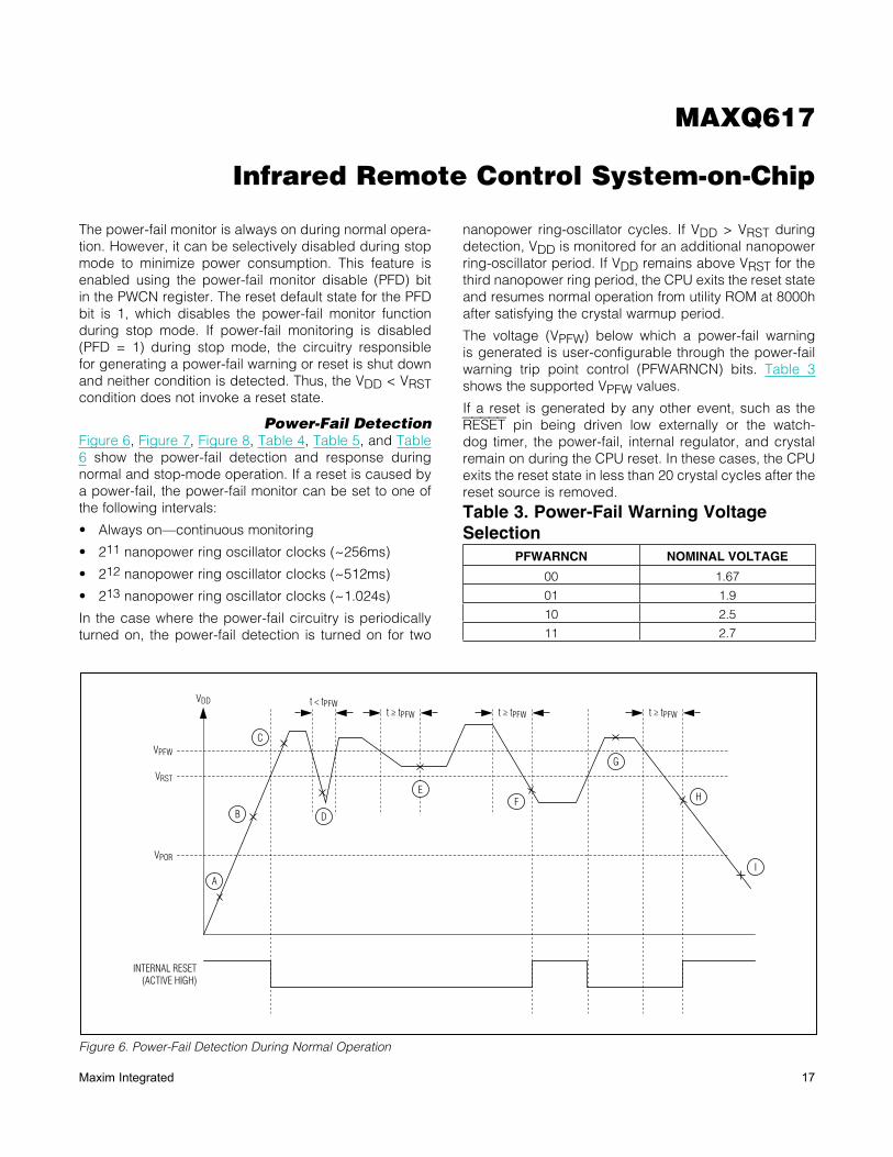
Figure 6. Power-Fail Detection During Normal Operation
The power-fail monitor is always on during normal opera-tion. However, it can be selectively disabled during stop mode to minimize power consumption. This feature is enabled using the power-fail monitor disable (PFD) bit in the PWCN register. The reset default state for the PFD bit is 1, which disables the power-fail monitor function during stop mode. If power-fail monitoring is disabled (PFD = 1) during stop mode, the circuitry responsible for generating a power-fail warning or reset is shut down and neither condition is detected. Thus, the VDD < VRST condition does not invoke a reset state.
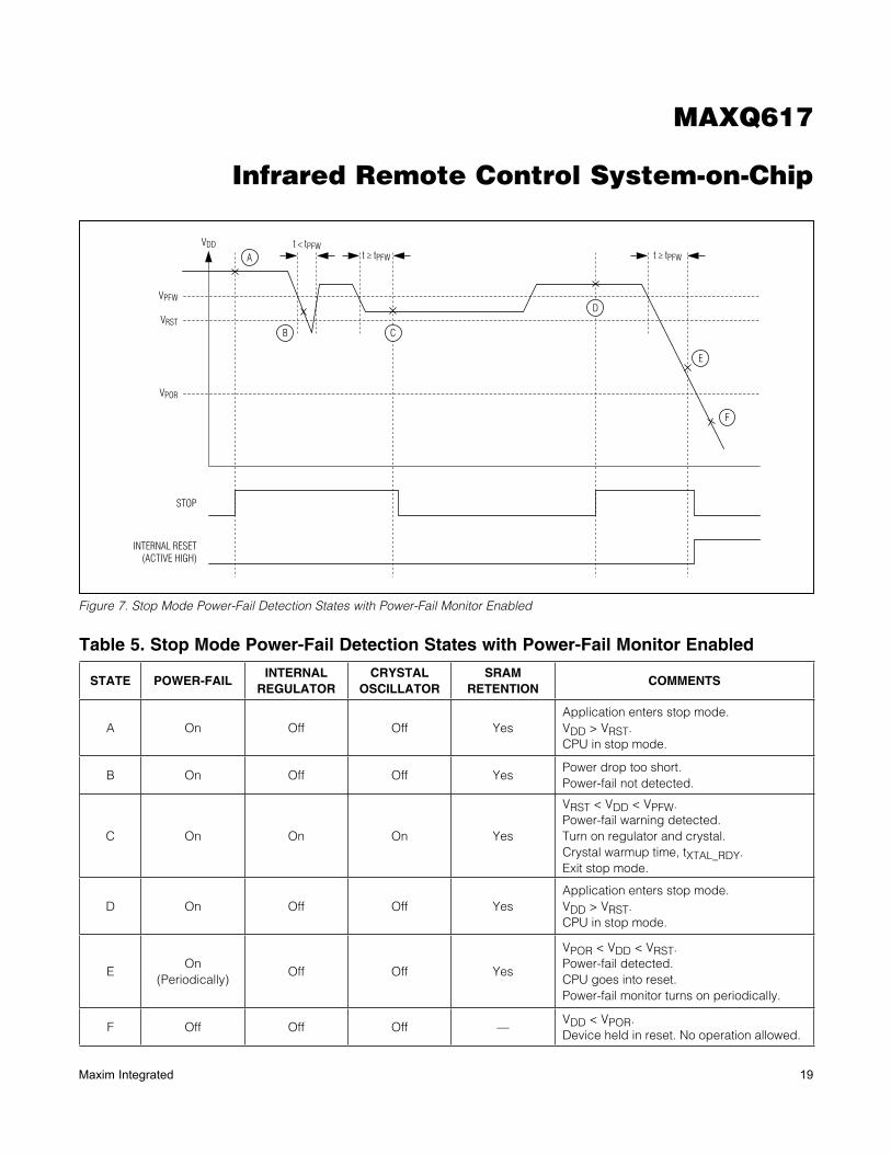
Power-Fail DetectionFigure 6, Figure 7, Figure 8, Table 4, Table 5, and Table 6 show the power-fail detection and response during normal and stop-mode operation. If a reset is caused by a power-fail, the power-fail monitor can be set to one of the following intervals:
• Always on—continuous monitoring
• 211 nanopower ring oscillator clocks (~256ms)
• 212 nanopower ring oscillator clocks (~512ms)
• 213 nanopower ring oscillator clocks (~1.024s)
In the case where the power-fail circuitry is periodically turned on, the power-fail detection is turned on for two
nanopower ring-oscillator cycles. If VDD > VRST during detection, VDD is monitored for an additional nanopower ring-oscillator period. If VDD remains above VRST for the third nanopower ring period, the CPU exits the reset state and resumes normal operation from utility ROM at 8000h after satisfying the crystal warmup period.
The voltage (VPFW) below which a power-fail warning is generated is user-configurable through the power-fail warning trip point control (PFWARNCN) bits. Table 3 shows the supported VPFW values.
If a reset is generated by any other event, such as the RESET pin being driven low externally or the watch-dog timer, the power-fail, internal regulator, and crystal remain on during the CPU reset. In these cases, the CPU exits the reset state in less than 20 crystal cycles after the reset source is removed.
Table 3. Power-Fail Warning Voltage Selection
PFWARNCN NOMINAL VOLTAGE
00 1.67
01 1.9
10 2.5
11 2.7
A
B
C
D
F
G
H
I
E
VDD
VPFW
VRST
VPOR
INTERNAL RESET(ACTIVE HIGH)
t < tPFWt ≥ tPFW t ≥ tPFW t ≥ tPFW
MAXQ617
Infrared Remote Control System-on-Chip
18Maxim Integrated
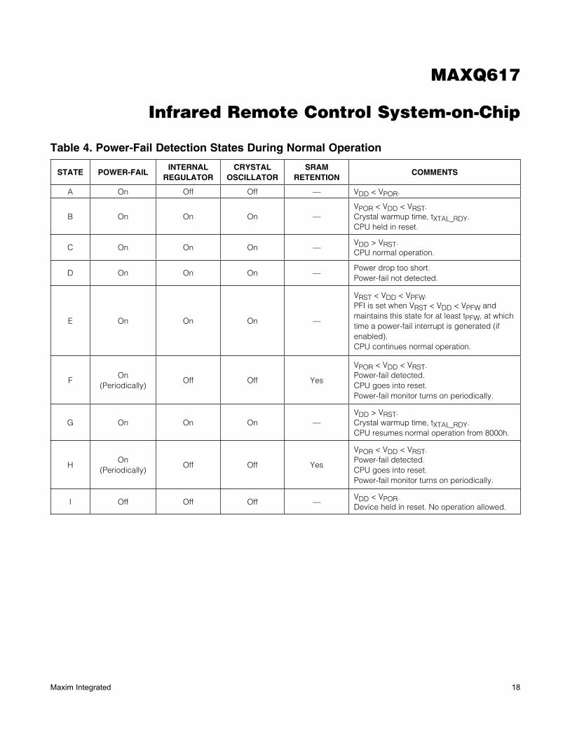
Table 4. Power-Fail Detection States During Normal Operation
STATE POWER-FAILINTERNAL
REGULATORCRYSTAL
OSCILLATORSRAM
RETENTIONCOMMENTS
A On Off Off — VDD < VPOR.
B On On On —VPOR < VDD < VRST.Crystal warmup time, tXTAL_RDY.CPU held in reset.
C On On On —VDD > VRST.CPU normal operation.
D On On On —Power drop too short.Power-fail not detected.
E On On On —
VRST < VDD < VPFW.PFI is set when VRST < VDD < VPFW and maintains this state for at least tPFW, at which time a power-fail interrupt is generated (if enabled).CPU continues normal operation.
FOn
(Periodically)Off Off Yes
VPOR < VDD < VRST.Power-fail detected.CPU goes into reset.Power-fail monitor turns on periodically.
G On On On —VDD > VRST.Crystal warmup time, tXTAL_RDY.CPU resumes normal operation from 8000h.
HOn
(Periodically)Off Off Yes
VPOR < VDD < VRST.Power-fail detected.CPU goes into reset.Power-fail monitor turns on periodically.
I Off Off Off —VDD < VPOR.Device held in reset. No operation allowed.
MAXQ617
Infrared Remote Control System-on-Chip
19Maxim Integrated
Figure 7. Stop Mode Power-Fail Detection States with Power-Fail Monitor Enabled
Table 5. Stop Mode Power-Fail Detection States with Power-Fail Monitor Enabled
STATE POWER-FAILINTERNAL
REGULATORCRYSTAL
OSCILLATORSRAM
RETENTIONCOMMENTS
A On Off Off YesApplication enters stop mode.VDD > VRST.CPU in stop mode.
B On Off Off YesPower drop too short.Power-fail not detected.
C On On On Yes
VRST < VDD < VPFW.Power-fail warning detected.Turn on regulator and crystal.Crystal warmup time, tXTAL_RDY.Exit stop mode.
D On Off Off YesApplication enters stop mode.VDD > VRST.CPU in stop mode.
EOn
(Periodically)Off Off Yes
VPOR < VDD < VRST.Power-fail detected.CPU goes into reset.Power-fail monitor turns on periodically.
F Off Off Off —VDD < VPOR.Device held in reset. No operation allowed.
VPFW
VRST
VPOR
A
B C
D
E
F
VDD t < tPFWt ≥ tPFW t ≥ tPFW
STOP
INTERNAL RESET(ACTIVE HIGH)

MAXQ617
Infrared Remote Control System-on-Chip
20Maxim Integrated
Figure 8. Stop Mode Power-Fail Detection with Power-Fail Monitor Disabled
Table 6. Stop Mode Power-Fail Detection States with Power-Fail Monitor Disabled
STATE POWER-FAILINTERNAL
REGULATORCRYSTAL
OSCILLATORSRAM
RETENTIONCOMMENTS
A Off Off Off YesApplication enters stop mode.VDD > VRST.CPU in stop mode.
B Off Off Off YesVDD < VPFW.Power-fail not detected because power-fail monitor is disabled.
C On On On Yes
VRST < VDD < VPFW.An interrupt occurs that causes the CPU to exit stop mode.Power-fail monitor is turned on, detects a power-fail warning, and sets the power-fail interrupt flag.Turn on regulator and crystal.Crystal warmup time, tXTAL_RDY.On stop mode exit, CPU vectors to the higher priority of power-fail and the interrupt that causes stop mode exit.
VPFW
VRST
VPOR
VDD
A
BC
D
E
F
STOP
INTERRUPT
INTERNAL RESET(ACTIVE HIGH)

MAXQ617
Infrared Remote Control System-on-Chip
21Maxim Integrated
Table 6. Stop Mode Power-Fail Detection States with Power-Fail Monitor Disabled (continued)
Applications Information
The low-power, high-performance RISC architecture of this device makes it an excellent fit for many portable or battery-powered applications. It is ideally suited for appli-cations such as universal remote controls that require the cost-effective integration of IR transmit/receive capability.
Grounds and BypassingCareful PCB layout significantly minimizes system-level digital noise that could interact with the microcontroller or peripheral components. The use of multilayer boards is essential to allow the use of dedicated power planes. The area under any digital components should be a con-tinuous ground plane if possible. Keep bypass capacitor leads short for best noise rejection and place the capaci-tors as close to the leads of the devices as possible.
CMOS design guidelines for any semiconductor require that no pin be taken above VDD or below GND. Violation of this guideline can result in a hard failure (damage to the silicon inside the device) or a soft failure (uninten-tional modification of memory contents). Voltage spikes above or below the device’s absolute maximum ratings can potentially cause a devastating IC latchup.
Microcontrollers commonly experience negative volt-age spikes through either their power pins or general-purpose I/O pins. Negative voltage spikes on power pins are especially problematic as they directly couple to the internal power buses. Devices such as keypads can con-duct electrostatic discharges directly into the microcon-troller and seriously damage the device. System design-ers must protect components against these transients that can corrupt system memory.
STATE POWER-FAILINTERNAL
REGULATORCRYSTAL
OSCILLATORSRAM
RETENTIONCOMMENTS
D Off Off Off YesApplication enters stop mode.VDD > VRST.CPU in stop mode.
EOn
(Periodically)Off Off Yes
VPOR < VDD < VRST.An interrupt occurs that causes the CPU to exit stop mode.Power-fail monitor is turned on, detects a power-fail, and puts CPU in reset.Power-fail monitor is turned on periodically.
F Off Off Off —VDD < VPOR.Device held in reset. No operation allowed.
MAXQ617
Infrared Remote Control System-on-Chip
22Maxim Integrated
Note: The 4-digit suffix “-XXXX” indicates a device preprogrammed at Maxim Integrated with proprietary customer-supplied soft-ware. For more information on factory preprogramming of this device, contact Maxim Integrated at support.maximintegrated.com/micro.+Denotes a lead(Pb)-free/RoHS-compliant package.T = Tape and reel.
Additional Documentation
Engineers must have the following documents to fully use this device:
• This data sheet, containing pin descriptions, feature overviews, and electrical specifications.
• The device-appropriate user guide, containing detailed information and programming guidelines for core features and peripherals.
• Errata sheets for specific revisions noting deviations from published specifications.
For information regarding these documents, visit Technical Support at support.maximintegrated.com/micro.
Development and Technical Support
Contact technical support for information about highly versatile, affordable development tools, available from Maxim Integrated and third-party vendors.
• Evaluation kits
• Compilers
• Integrated development environments (IDEs)
• USB interface modules for programming and debugging
For technical support, go to support.maximintegrated.com/micro.
Ordering Information/Selector Guide
Package Information
For the latest package outline information and land patterns (footprints), go to www.maximintegrated.com/packages. Note that a “+”, “#”, or “-” in the package code indicates RoHS status only. Package drawings may show a different suffix character, but the drawing pertains to the package regardless of RoHS status.
PART TEMP RANGEOPERATING VOLTAGE (V)
PROGRAM MEMORY (KB)
DATA MEMORY (KB)
GPIO PIN-PACKAGE
MAXQ617V-XXXX+T -20NC to +70NC 1.67 to 3.6 80 Flash 4 10 16 WLP
PACKAGE TYPE PACKAGE CODE OUTLINE NO. LAND PATTERN NO.
16 WLP W162K2+1 21-0491Refer to
Application Note 1891
MAXQ617
Infrared Remote Control System-on-Chip
23Maxim Integrated
Appendix A
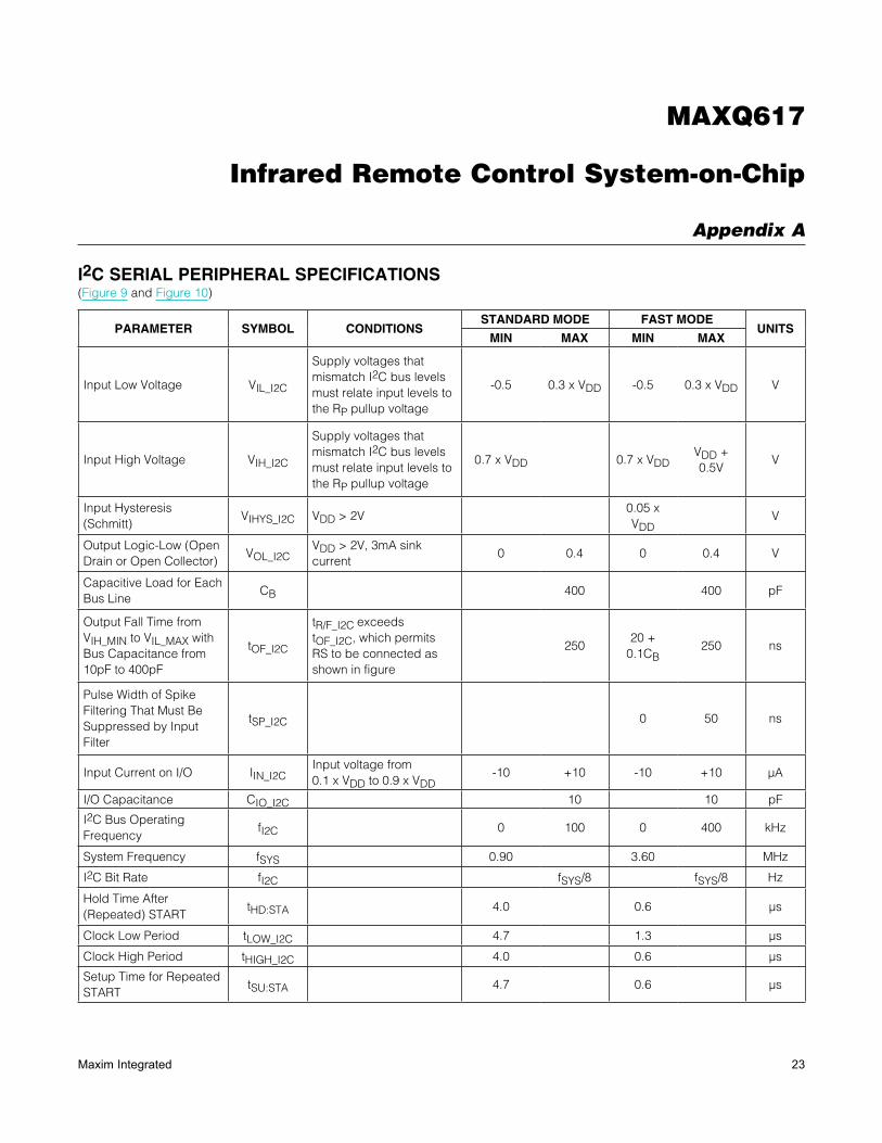
I2C SERIAL PERIPHERAL SPECIFICATIONS(Figure 9 and Figure 10)
PARAMETER SYMBOL CONDITIONSSTANDARD MODE FAST MODE
UNITSMIN MAX MIN MAX
Input Low Voltage VIL_I2C
Supply voltages that mismatch I2C bus levels must relate input levels to the RP pullup voltage
-0.5 0.3 x VDD -0.5 0.3 x VDD V
Input High Voltage VIH_I2C
Supply voltages that mismatch I2C bus levels must relate input levels to the RP pullup voltage
0.7 x VDD 0.7 x VDDVDD + 0.5V
V
Input Hysteresis (Schmitt)
VIHYS_I2C VDD > 2V0.05 x VDD
V
Output Logic-Low (Open Drain or Open Collector)
VOL_I2CVDD > 2V, 3mA sink current
0 0.4 0 0.4 V
Capacitive Load for Each Bus Line
CB 400 400 pF
Output Fall Time from VIH_MIN to VIL_MAX with Bus Capacitance from 10pF to 400pF
tOF_I2C
tR/F_I2C exceeds tOF_I2C, which permits RS to be connected as shown in figure
25020 +
0.1CB250 ns
Pulse Width of Spike Filtering That Must Be Suppressed by Input Filter
tSP_I2C 0 50 ns
Input Current on I/O IIN_I2CInput voltage from 0.1 x VDD to 0.9 x VDD
-10 +10 -10 +10 FA
I/O Capacitance CIO_I2C 10 10 pF
I2C Bus Operating Frequency
fI2C 0 100 0 400 kHz
System Frequency fSYS 0.90 3.60 MHz
I2C Bit Rate fI2C fSYS/8 fSYS/8 Hz
Hold Time After (Repeated) START
tHD:STA 4.0 0.6 Fs
Clock Low Period tLOW_I2C 4.7 1.3 Fs
Clock High Period tHIGH_I2C 4.0 0.6 Fs
Setup Time for Repeated START
tSU:STA 4.7 0.6 Fs
MAXQ617
Infrared Remote Control System-on-Chip
24Maxim Integrated
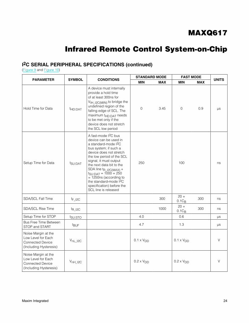
I2C SERIAL PERIPHERAL SPECIFICATIONS (continued)(Figure 9 and Figure 10)
PARAMETER SYMBOL CONDITIONSSTANDARD MODE FAST MODE
UNITSMIN MAX MIN MAX
Hold Time for Data tHD:DAT
A device must internally provide a hold time of at least 300ns for VIH_I2C(MIN) to bridge the undefined region of the falling edge of SCL. The maximum tHD:DAT needs to be met only if the device does not stretch the SCL low period
0 3.45 0 0.9 Fs
Setup Time for Data tSU:DAT
A fast-mode I2C bus device can be used in a standard-mode I2C bus system; if such a device does not stretch the low period of the SCL signal, it must output the next data bit to the SDA line tR_I2C(MAX) + tSU:DAT = 1000 + 250 = 1250ns (according to the standard-mode I2C specification) before the SCL line is released
250 100 ns
SDA/SCL Fall Time tF_I2C 30020 +
0.1CB300 ns
SDA/SCL Rise Time tR_I2C 100020 +
0.1CB300 ns
Setup Time for STOP tSU:STO 4.0 0.6 Fs
Bus Free Time Between STOP and START
tBUF 4.7 1.3 Fs
Noise Margin at the Low Level for Each Connected Device (Including Hysteresis)
VnL_I2C 0.1 x VDD 0.1 x VDD V
Noise Margin at the Low Level for Each Connected Device (Including Hysteresis)
VnH_I2C 0.2 x VDD 0.2 x VDD V
MAXQ617
Infrared Remote Control System-on-Chip
25Maxim Integrated
I2C Serial Diagrams
Figure 9. Series Resistors (RS) for Protecting Against High-Voltage Spikes
Figure 10. I2C Bus Controller Timing Diagram
SDA
SCL
RS RS
I2CDEVICE
RS RS
I2CDEVICE
RP RP
VDD
MAXQ617
SDA
SCL
S SR P S
tF_I2C tR_I2C
tLOW_I2C
tHIGH_I2CtHD:STA
tSU:DAT tSU:STA
tSU:STO
tBUF
tHD:DAT
NOTE: TIMING REFERENCED TO VIH_I2C(MIN) AND VIL_I2C(MAX).
MAXQ617
Infrared Remote Control System-on-Chip
26Maxim Integrated
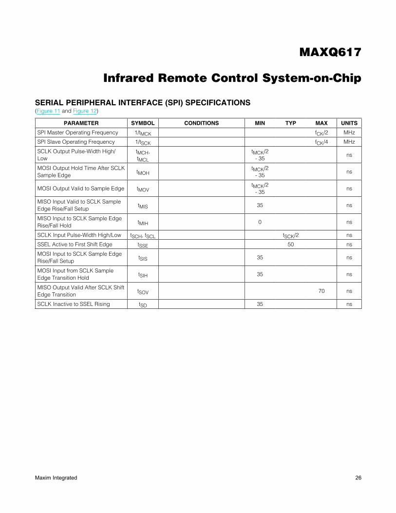
SERIAL PERIPHERAL INTERFACE (SPI) SPECIFICATIONS(Figure 11 and Figure 12)
PARAMETER SYMBOL CONDITIONS MIN TYP MAX UNITS
SPI Master Operating Frequency 1/tMCK fCK/2 MHz
SPI Slave Operating Frequency 1/tSCK fCK/4 MHz
SCLK Output Pulse-Width High/Low
tMCH, tMCL
tMCK/2 - 35
ns
MOSI Output Hold Time After SCLK Sample Edge
tMOHtMCK/2
- 35ns
MOSI Output Valid to Sample Edge tMOVtMCK/2
- 35ns
MISO Input Valid to SCLK Sample Edge Rise/Fall Setup
tMIS 35 ns
MISO Input to SCLK Sample Edge Rise/Fall Hold
tMIH 0 ns
SCLK Input Pulse-Width High/Low tSCH, tSCL tSCK/2 ns
SSEL Active to First Shift Edge tSSE 50 ns
MOSI Input to SCLK Sample Edge Rise/Fall Setup
tSIS 35 ns
MOSI Input from SCLK Sample Edge Transition Hold
tSIH 35 ns
MISO Output Valid After SCLK Shift Edge Transition
tSOV 70 ns
SCLK Inactive to SSEL Rising tSD 35 ns
MAXQ617
Infrared Remote Control System-on-Chip
27Maxim Integrated
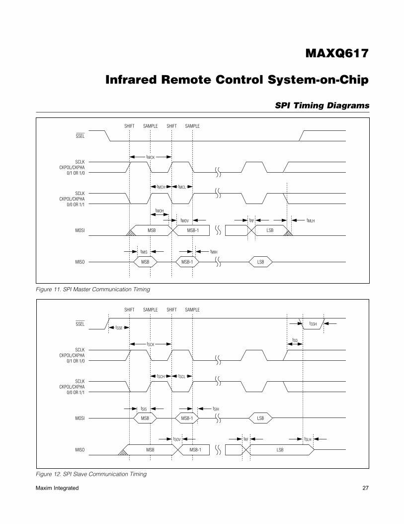
SPI Timing Diagrams
Figure 11. SPI Master Communication Timing
Figure 12. SPI Slave Communication Timing
SSEL
SCLKCKPOL/CKPHA
0/1 OR 1/0
SCLKCKPOL/CKPHA
0/0 OR 1/1
MOSI
MISO
LSB
LSB
SHIFT SAMPLE SHIFT SAMPLE
tMCK
tMCH
tMOH
tMIS
tMOV tRF tMLH
tMIH
tMCL
MSB MSB-1
MSB MSB-1
SHIFT SAMPLE SHIFT SAMPLE
SSEL
SCLKCKPOL/CKPHA
0/1 OR 1/0
SCLKCKPOL/CKPHA
0/0 OR 1/1
MOSI
MISO
tSSE
tSCK
tSCH tSCL
tSIS
tSOV tSLH
tSSH
tSD
tRF
tSIH
MSB MSB-1
MSB MSB-1
LSB
LSB
MAXQ617
Infrared Remote Control System-on-Chip
28Maxim Integrated
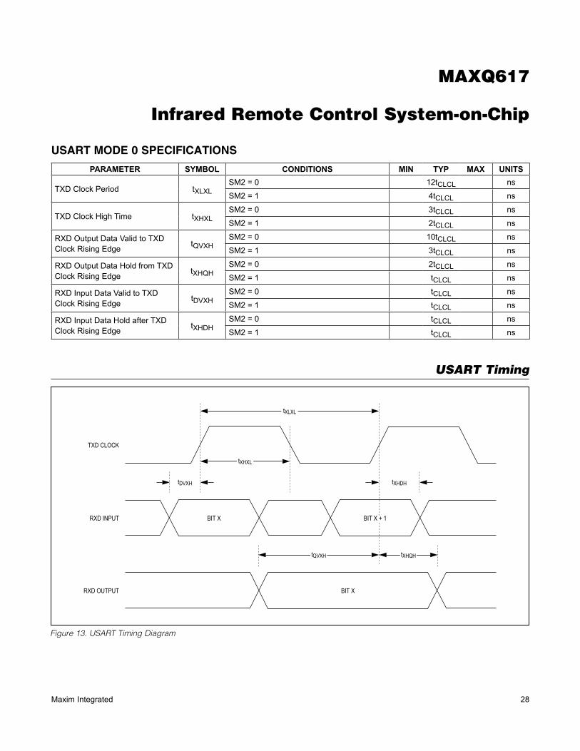
Figure 13. USART Timing Diagram
USART Timing
USART MODE 0 SPECIFICATIONS
PARAMETER SYMBOL CONDITIONS MIN TYP MAX UNITS
TXD Clock Period tXLXLSM2 = 0 12tCLCL ns
SM2 = 1 4tCLCL ns
TXD Clock High Time tXHXLSM2 = 0 3tCLCL ns
SM2 = 1 2tCLCL ns
RXD Output Data Valid to TXD Clock Rising Edge tQVXH
SM2 = 0 10tCLCL ns
SM2 = 1 3tCLCL ns
RXD Output Data Hold from TXD Clock Rising Edge tXHQH
SM2 = 0 2tCLCL ns
SM2 = 1 tCLCL ns
RXD Input Data Valid to TXD Clock Rising Edge tDVXH
SM2 = 0 tCLCL ns
SM2 = 1 tCLCL ns
RXD Input Data Hold after TXD Clock Rising Edge tXHDH
SM2 = 0 tCLCL ns
SM2 = 1 tCLCL ns
tXLXL
tXHXL
tDVXH tXHDH
tQVXH tXHQH
TXD CLOCK
RXD INPUT
RXD OUTPUT
BIT X
BIT X
BIT X + 1
MAXQ617
Infrared Remote Control System-on-Chip
Maxim Integrated cannot assume responsibility for use of any circuitry other than circuitry entirely embodied in a Maxim Integrated product. No circuit patent licenses are implied. Maxim Integrated reserves the right to change the circuitry and specifications without notice at any time. The parametric values (min and max limits) shown in the Electrical Characteristics table are guaranteed. Other parametric values quoted in this data sheet are provided for guidance.
Maxim Integrated 160 Rio Robles, San Jose, CA 95134 USA 1-408-601-1000 29© 2013 Maxim Integrated Products, Inc. Maxim Integrated and the Maxim Integrated logo are trademarks of Maxim Integrated Products, Inc.
Revision History
REVISIONNUMBER
REVISIONDATE
DESCRIPTIONPAGES
CHANGED
0 12/13 Initial release —