Embed Size (px)
Citation preview

5/13/2018 Main Report - slidepdf.com
http://slidepdf.com/reader/full/main-report-55a7524402170 1/52
1
Global Institute of TechnologyJaipur
Session 2010-2011
CERTIFICATE
This is to certify that Shobhit Bahri, Udita Shah, Tushar Jain and Vaibhav Agarwal students of B.Tech VIII Semester (Electronics & Communication Engineering ) have Design and developed aMajor project on “TALKING VOLTMETER ” in the partial fulfillment of the award of Bachelor
of Engineering Degree by University of Rajasthan.
Project Coordinator Guide
Mr.R.N.Vishnoi Mr. J.D.Jain
Place: G.I.T,Jaipur
Date:

5/13/2018 Main Report - slidepdf.com
http://slidepdf.com/reader/full/main-report-55a7524402170 2/52
2
ACKNOWLEDGEMENT
We are very grateful to Mr. J.P.Aggarwal, HOD of Electronics & Communication
department, for the help provided in completing the Major project assigned to us. We owe
our thanks to Mr. J.D.Jain, to guide us and solve our problems during the project.
We are also thankful to Mr.R.N.Vishnoi sir for his motivation to us to undergo this
major project.
Last but not least, we pay our sincere thanks and gratitude to Mr. Babulal Sharma sir
for making our project valuable and fruitful.
We are also thankful, to all our colleagues for their co-operation and support.
Shobhit Bahri
Udita Shah
Tushar Jain
Vaibhav Agarwal
Date:Place:

5/13/2018 Main Report - slidepdf.com
http://slidepdf.com/reader/full/main-report-55a7524402170 3/52
3
PURPOSE
The purpose of the project is to make a tool which should be beneficial to any person who actively
works in the lab. It is mainly used to measure voltage, the average of voltage and the value of
minimum & maximum voltage. Frequency measurement is also done with great accuracy from
about 10Hz to 100k Hz. All the readings are given out by the help of speakers; therefore, it is a very
useful tool. It is even advantageous for some person to utilize this device instead of standard lab
equipment.
The programming is done using microcontrollers and various IC’s have been used for various
purposes which have been defined in the following pages.
SOURCE OF THE PROJECT IDEA
We got this idea while surfing on net. Further this idea was encouraged by our project guide
Mr.J.D.Jain sir. Also Mr.R.N.Vishnoi sir also helped us with the idea. We thought of the practical
advantage of this project, analyzed its uses and came to a conclusion that this may be advantageous
to everybody in labs. So this inspired us to work on this project and we tried to make something
fruitful.
THEORITICAL BACKGROUND
1. ATMEGA 32

5/13/2018 Main Report - slidepdf.com
http://slidepdf.com/reader/full/main-report-55a7524402170 4/52
4
Overview:
The ATmega32 is a low-power CMOS 8-bit microcontroller based on the AVR enhanced RISC
architecture. By executing powerful instructions in a single clock cycle, the ATmega32 achieves
throughputs approaching 1 MIPS per MHz allowing the system designed to optimize power
consumption versus processing speed.
The AVR core combines a rich instruction set with 32 general purpose working registers. All the 32
registers are directly connected to the Arithmetic Logic Unit (ALU), allowing two independent
registers to be accessed in one single instruction executed in one clock cycle. The resulting
architecture is more code efficient while achieving throughputs up to ten times faster than
conventional CISC microcontrollers.
The ATmega32 provides the following features: 32K bytes of In-System Programmable Flash
Program memory with Read-While-Write capabilities, 1024 bytes EEPROM, 2K byte SRAM, 32
general purpose I/O lines, 32 general purpose working registers, a JTAG interface for Boundary
scan, On-chip Debugging support and programming, three flexible Timer/Counters with compare
modes, Internal and External Interrupts, a serial programmable USART, a byte oriented Two-wire
Serial Interface, an 8-channel, 10-bit ADC with optional differential input stage with programmable
gain (TQFP package only), a programmable Watchdog Timer with Internal Oscillator, an SPI serial
port, and six software selectable power saving modes. The Idle mode stops the CPU while allowingthe USART, Two-wire interface, A/D Converter, SRAM, Timer/Counters, SPI port, and interrupt
system to continue functioning. The Power-down mode saves the register contents but freezes the
Oscillator, disabling all other chip functions until the next External Interrupt or Hardware Reset. In
Power-save mode, the Asynchronous Timer continues to run, allowing the user to maintain a timer
base while the rest of the device is sleeping. The ADC Noise Reduction mode stops the CPU and all
I/O modules except Asynchronous Timer and ADC, to minimize switching noise during ADC
conversions. In Standby mode, the crystal/resonator Oscillator is running while the rest of the device
is sleeping. This allows very fast start-up combined with low-power consumption. In Extended
Standby mode, both the main Oscillator and the Asynchronous Timer continue to run.
The device is manufactured using Atmel’s high density nonvolatile memory technology. The
Onchip ISP Flash allows the program memory to be reprogrammed in-system through an SPI serial
interface, by a conventional nonvolatile memory programmer, or by an On-chip Boot program

5/13/2018 Main Report - slidepdf.com
http://slidepdf.com/reader/full/main-report-55a7524402170 5/52
5
running on the AVR core. The boot program can use any interface to download the application
program in the Application Flash memory. Software in the Boot Flash section will continue to run
while the Application Flash section is updated, providing true Read-While-Write operation. By
combining an 8-bit RISC CPU with In-System Self-Programmable Flash on a monolithic chip, the
Atmel ATmega32 is a powerful microcontroller that provides a highly-flexible and cost-effectivesolution to many embedded control applications.
Features
• High-performance, Low-power AVR® 8-bit Microcontroller
• Advanced RISC Architecture
– 131 Powerful Instructions – Most Single-clock Cycle Execution
– 32 x 8 General Purpose Working Registers
– Fully Static Operation
– 2K Byte Internal SRAM
– In-System Programming by On-chip Boot Program True Read-While-Write Operation
– Programming Lock for Software Security
– Two 8-bit Timer/Counters
– One 16-bit Timer/Counter
– Real Time Counter with Separate Oscillator
– 8-channel, 10-bit ADC
-8 Single-ended Channels
– On-chip Analog Comparator
– Internal Calibrated RC Oscillator
– External and Internal Interrupt Sources
– 32 Programmable I/O Lines
– 40-pin PDIP
–Operating Voltages
– 2.7 - 5.5V for ATmega32L
– 4.5 - 5.5V for ATmega32
– 0 - 16 MHz speed grades for ATmega32
Pin Configuration:

5/13/2018 Main Report - slidepdf.com
http://slidepdf.com/reader/full/main-report-55a7524402170 6/52
6
Fig.1 PIN diagram
Pin Description:
VCC : Digital supply voltage.
GND : Ground.
Port A (PA7-PA0) : Port A serves as the analog inputs to the A/D Converter.

5/13/2018 Main Report - slidepdf.com
http://slidepdf.com/reader/full/main-report-55a7524402170 7/52
7
Port A also serves as an 8-bit bi-directional I/O port, if the A/D Converter is not used. Port pins can
provide internal pull-up resistors (selected for each bit). The Port A output buffers have symmetrical
drive characteristics with both high sink and source capability. When pins PA0 to PA7 are used as
inputs and are externally pulled low, they will source current if the internal pull-up resistors are
activated. The Port A pins are tri-stated when a reset condition becomes active, even if the clock isnot running.
Port B (PB7-PB0): Port B is an 8-bit bi-directional I/O port with internal pull-up resistors (selected
for each bit). The Port B output buffers have symmetrical drive characteristics with both high sink
and source capability. As inputs, Port B pins that are externally pulled low will source current if the
pull-up resistors are activated. The Port B pins are tri-stated when a reset condition becomes active,
even if the clock is not running.
Port C (PC7-PC0): Port C is an 8-bit bi-directional I/O port with internal pull-up resistors (selected
for each bit). The Port C output buffers have symmetrical drive characteristics with both high sink
and source capability. As inputs, Port C pins that are externally pulled low will source current if the
pull-up resistors are activated. The Port C pins are tri-stated when a reset condition becomes active,
even if the clock is not running. If the JTAG interface is enabled, the pull-up resistors on pins
PC5(TDI), PC3(TMS) and PC2(TCK) will be activated even if a reset occurs. The TD0 pin is tri-
stated unless TAP states that shift out data are entered.
Port D (PD7-PD0): Port D is an 8-bit bi-directional I/O port with internal pull-up resistors (selected
for each bit). The Port D output buffers have symmetrical drive characteristics with both high sink
and source capability. As inputs, Port D pins that are externally pulled low will source current if the
pull-up resistors are activated. The Port D pins are tri-stated when a reset condition becomes active,
even if the clock is not running.
RESET: Reset Input. A low level on this pin for longer than the minimum pulse length will
generate a reset, even if the clock is not running.
XTAL1: Input to the inverting Oscillator amplifier and input to the internal clock operating circuit.
XTAL2: Output from the inverting Oscillator amplifier.
5/13/2018 Main Report - slidepdf.com
http://slidepdf.com/reader/full/main-report-55a7524402170 8/52
8
AVCC: AVCC is the supply voltage pin for Port A and the A/D Converter. It should be externally
connected to VCC, even if the ADC is not used. If the ADC is used, it should be connected to VCC
through a low-pass filter.
AREF: AREF is the analog reference pin for the A/D Converter.
Fig.2 Atmega32 IC
2. LCD (LIQUID CRYSTAL DISPLAY)
LCDs with a small number of segments, such as those used in digital watches and pocket
calculators, have a single electrical contact for each segment. An external dedicated Electronic
circuit supplies an electric charge to control each segment. This display structure is unwieldy for
more than a few display elements.

5/13/2018 Main Report - slidepdf.com
http://slidepdf.com/reader/full/main-report-55a7524402170 9/52
9
Fig. 3 LCD Screen
Small monochrome displays such as those found in personal organizers, or older laptop screens have
a passive-matrix structure employing Super-twisted nematic display (STN) or double-layer STN
(DSTN) technology (DSTN corrects a color-shifting problem with STN). Each row or column of the
display has a single electrical circuit. The pixels are addressed one at a time by row and column
addresses. This type of display is called a passive matrix because the pixel must retain its state
between refreshes without the benefit of a steady electrical charge. As the number of pixels (and,
correspondingly, columns and rows) increases, this type of display becomes less feasible. Very slow
response time and poor contrast are typical of passive-matrix LCDs.

5/13/2018 Main Report - slidepdf.com
http://slidepdf.com/reader/full/main-report-55a7524402170 10/52
10
Fig. 4 LCD Frame
High display resolution color displays such as modern LCD computer display and televisions use an
Active-matrix liquid crystal display matrix structure. A matrix of thin-film transistors TFTs is added
to the polarizing and color filters. Each pixel has its own dedicated transistor, allowing each column
line to access one pixel. When a row line is activated, all of the column lines are connected to a row
of pixels and the correct voltage is driven onto all of the column lines. The row line is then
deactivated and the next row line is activated. All of the row lines are activated in sequence during a
refresh operation. Active matrix displays are much brighter and sharper than passive-matrix displaysof the same size, and generally have quicker response times, producing much better images.

5/13/2018 Main Report - slidepdf.com
http://slidepdf.com/reader/full/main-report-55a7524402170 11/52
11
CRYSTAL OSCILLATOR
A crystal oscillator is an electronic oscillator circuit that uses the mechanical resonance of a
vibrating crystal of piezoelectric material to create an electrical signal with a very precise frequency.
This frequency is commonly used to keep track of time (as in quartz wristwatches), to provide a
stable clock signal for digital integrated circuits, and to stabilize frequencies for radio transmitters
and receivers. The most common type of piezoelectric resonator used is the quartz crystal, so
oscillator circuits designed around them became known as “crystal oscillators.”
Quartz crystals are manufactured for frequencies from a few tens of kilohertz to tens of megahertz.
More than two billion (2×10⁹) crystals are manufactured annually. Most are used for consumer
devices such as wristwatches, clocks, radios, computers, and cellphones. Quartz crystals are also
found inside test and measurement equipment, such as counters, signal generators, and
oscilloscopes.
A crystal is a solid in which the constituent atoms, molecules, or ions are packed in a regularly
ordered, repeating pattern extending in all three spatial dimensions.
Almost any object made of an elastic material could be used like a crystal, with appropriate
transducers, since all objects have natural resonant frequencies of vibration. For example, steel is
very elastic and has a high speed of sound. It was often used in mechanical filters before quartz. The
resonant frequency depends on size, shape, elasticity, and the speed of sound in the material. High-
frequency crystals are typically cut in the shape of a simple, rectangular plate. Low-frequencycrystals, such as those used in digital watches, are typically cut in the shape of a tuning fork . For
applications not needing very precise timing, a low-cost ceramic resonator is often used in place of a
quartz crystal.
When a crystal of quartz is properly cut and mounted, it can be made to distort in an electric field by
applying a voltage to an electrode near or on the crystal. This property is known as piezoelectricity.
When the field is removed, the quartz will generate an electric field as it returns to its previous
shape, and this can generate a voltage. The result is that a quartz crystal behaves like a circuit
composed of an inductor , capacitor and resistor , with a precise resonant frequency. (See RLC
circuit.)
Quartz has the further advantage that its elastic constants and its size change in such a way that the
frequency dependence on temperature can be very low. The specific characteristics will depend on
the mode of vibration and the angle at which the quartz is cut (relative to its crystallographic axes).
Therefore, the resonant frequency of the plate, which depends on its size, will not change much,

5/13/2018 Main Report - slidepdf.com
http://slidepdf.com/reader/full/main-report-55a7524402170 12/52
12
either. This means that a quartz clock, filter or oscillator will remain accurate. For critical
applications the quartz oscillator is mounted in a temperature-controlled container, called a crystal
oven, and can also be mounted on shock absorbers to prevent perturbation by external mechanical
vibrations.
Fig. 5 Crystal Oscillator
3. LM7805

5/13/2018 Main Report - slidepdf.com
http://slidepdf.com/reader/full/main-report-55a7524402170 13/52
13
The 78xx (sometimes LM78xx) is a family of self-contained fixed linear voltage regulator integrated circuit. The 78xx family is commonly used in electronic circuits requiring a regulated power supply due to their ease-of-use and low cost. For ICs within the family, the xx is replacedwith two digits, indicating the output voltage (for example, the 7805 has a 5 volt output, while the7812 produces 12 volts). The 78xx lines are positive voltage regulators: they produce a voltage thatis positive relative to a common ground. There is a related line of 79xx devices which are
complementary negative voltage regulators. 78xx and 79xx ICs can be used in combination to provide positive and negative supply voltages in the same circuit.
78xx ICs have three terminals These devices support an input voltage anywhere from a couple of volts over the intended output voltage, up to a maximum of 35 or 40 volts, and typically provide 1 or 1.5 amps of current (though smaller or larger packages may have a lower or higher current rating).
Fig. 6 LM7805
Advantages
• 78xx series ICs do not require additional components to provide a constant, regulated sourceof power, making them easy to use, as well as economical and efficient uses of space. Other voltage regulators may require additional components to set the output voltage level, or toassist in the regulation process. Some other designs (such as a switching power supply) mayneed substantial engineering expertise to implement.
• 78xx series ICs have built-in protection against a circuit drawing too much power. They have protection against overheating and short-circuits, making them quite robust in mostapplications. In some cases, the current-limiting features of the 78xx devices can provide protection not only for the 78xx itself, but also for other parts of the circuit.
•
Disadvantages
• The input voltage must always be higher than the output voltage by some minimum amount(typically 2 volts). This can make these devices unsuitable for powering some devices fromcertain types of power sources (for example, powering a circuit that requires 5 volts using 6-volt batteries will not work using a 7805).
• As they are based on a linear regulator design, the input current required is always the sameas the output current. As the input voltage must always be higher than the output voltage, thismeans that the total power (voltage multiplied by current) going into the 78xx will be more

5/13/2018 Main Report - slidepdf.com
http://slidepdf.com/reader/full/main-report-55a7524402170 14/52
14
than the output power provided. The extra input power is dissipated as heat. This means boththat for some applications an adequate heat sink must be provided, and also that a (oftensubstantial) portion of the input power is wasted during the process, rendering them lessefficient than some other types of power supplies. When the input voltage is significantlyhigher than the regulated output voltage (for example, powering a 7805 using a 24 volt power source), this inefficiency can be a significant issue.
• Even in larger packages, 78xx integrated circuits cannot supply as much power as manydesigns which use discrete components, and are generally inappropriate for applicationsrequiring more than a few amps of current.
7805 Voltage Regulator Pin-out
Fig. 7 LM7805 pin-out
1. LM7404
General characteristics:
There are several families of logic ICs numbered from 74xx00 onwards with letters (xx) in themiddle of the number to indicate the type of circuitry, eg 74LS00 and 74HC00. The original family(now obsolete) had no letters, eg 7400.
The 74LS (Low-power Schottky) family (like the original) uses TTL (Transistor-Transistor Logic)circuitry which is fast but requires more power than later families. The 74 series is often still calledthe 'TTL series' even though the latest ICs do not use TTL!

5/13/2018 Main Report - slidepdf.com
http://slidepdf.com/reader/full/main-report-55a7524402170 15/52
15
The 74HC family has High-speed CMOS circuitry, combining the speed of TTL with the very low power consumption of the 4000 series. They are CMOS ICs with the same pin arrangements as theolder 74LS family. Note that 74HC inputs cannot be reliably driven by 74LS outputs because thevoltage ranges used for logic 0 are not quite compatible, use 74HCT instead.
The 74HCT family is a special version of 74HC with 74LS TTL-compatible inputs so 74HCT can be safely mixed with 74LS in the same system. In fact 74HCT can be used as low-power direct
replacements for the older 74LS ICs in most circuits. The minor disadvantage of 74HCT is a lower immunity to noise, but this is unlikely to be a problem in most situations.
The CMOS circuitry used in the 74HC and 74HCT series ICs means that they are static sensitive.Touching a pin while charged with static electricity (from your clothes for example) may damagethe IC. In fact most ICs in regular use are quite tolerant and earthing your hands by touching a metalwater pipe or window frame before handling them will be adequate. ICs should be left in their protective packaging until you are ready to use them.
2. CODING-
MAIN.c
//Voice decompressor example#include <inttypes.h>#include <avr/io.h>#include <avr/interrupt.h>#include <util/delay.h>#include <avr/pgmspace.h>
//I like these definitions

5/13/2018 Main Report - slidepdf.com
http://slidepdf.com/reader/full/main-report-55a7524402170 16/52
16
#define begin {#define end }
//#define TableSize 1520 //refers to the following incl file//Contains the packed 2-bit codes for syntehsis//Generated by the program Make2code476.m
#include "LCD/lcd_lib.h"
unsigned char CurrentTable;
//reconstruction differentials// PCMvalue[4] = {-78, -16, 16, 78};volatile signed char PCMvalue[4] = {-20, -4, 4, 20};
volatile unsigned int outI, tableI;volatile unsigned char cycle ;volatile signed char out, lastout;volatile unsigned char p1, p2, p3, p4;volatile unsigned char packed ;
volatile unsigned int TableSize = 0;
unsigned char output[16] = " ";unsigned char buttonDown0 = 0, buttonDown1 = 0, buttonDown2 = 0, buttonDown3 = 0, buttonDown4 = 0;unsigned char metermode = 0;
float min, max, mean;unsigned int meanCount;
unsigned char takeFMeasure = 0;
int Ain;float voltage;
uint32_t frequency;unsigned char overflowCount = 0;unsigned char frequencyMeasured = 0;
#define LOGIC_THRESHOLD 2.0#define VREF 5.0
#include "voice.h"
//generate waveform at 7812 scamples/secISR (TIMER2_OVF_vect) begin
//compute next samplecycle = outI & 3; // out I modulo 4

5/13/2018 Main Report - slidepdf.com
http://slidepdf.com/reader/full/main-report-55a7524402170 17/52
17
if (cycle==0){
if (tableI<TableSize){
//unpack a table entry into 2-bit indexs// pgm_read_byte (address_short)
switch(CurrentTable){
case Volts_e: packed = pgm_read_byte(&Volts_wav[tableI]) ; break;
case Point_e: packed = pgm_read_byte(&Point_wav[tableI]) ; break;
case AllDigits_e: packed = pgm_read_byte(&AllDigits_wav[tableI]) ; break;
case Ready_e: packed = pgm_read_byte(&Ready_wav[tableI]) ; break;
case Beeplow_e: packed = pgm_read_byte(&Beeplow_wav[tableI]) ; break;
case Beephigh_e: packed = pgm_read_byte(&Beephigh_wav[tableI]) ; break;
case High_e: packed = pgm_read_byte(&High_wav[tableI]) ; break;
case Low_e: packed = pgm_read_byte(&Low_wav[tableI]) ; break;
case Mean_e: packed = pgm_read_byte(&Mean_wav[tableI]) ; break;
case Samples_e: packed = pgm_read_byte(&Samples_wav[tableI]) ; break;
case Over_e: packed = pgm_read_byte(&Over_wav[tableI]) ; break;
case Breakfast_e: packed = pgm_read_byte(&Breakfast_wav[tableI]) ; break;
case Hz_e: packed = pgm_read_byte(&Hz_wav[tableI]) ; break;
case Nosignal_e: packed = pgm_read_byte(&Nosignal_wav[tableI]) ; break;

5/13/2018 Main Report - slidepdf.com
http://slidepdf.com/reader/full/main-report-55a7524402170 18/52
18
}
//packed = DPCMAllDigits[tableI];p1 = (packed>>6) & 3 ;
p2 = (packed>>4) & 3 ;
p3 = (packed>>2) & 3 ;p4 = (packed & 3);tableI++ ;
} //end unpack table entry//compute the output and send to PWM
out = lastout + PCMvalue[p1] - (lastout>>3) ;}else if (cycle==1) //don't need to unpack yet--just ouput
out = lastout + PCMvalue[p2] - (lastout>>3) ;else if (cycle==2)
out = lastout + PCMvalue[p3] - (lastout>>3) ;else if (cycle==3)
out = lastout + PCMvalue[p4] - (lastout>>3) ;
//update outputsOCR0A = out + 128;
lastout = out;outI++;
//at end, turn off TCCROif (tableI>=TableSize){
TCCR0B = 0;say_next();
}end //ISR
void init_lcd(void) begin
LCDinit(); //initialize the displayLCDcursorOFF();LCDclr(); //clear the displayLCDGotoXY(0,0);LCDstring("Yo. Ima LCD.", 12);LCDGotoXY(0,1);LCDstring("Pick a Pgm, Yo.", 15);
end
void checkButtons(){
//Probe Button//very basic anti-bounce, as we only care about the rising edgeif(!(PINB & 0x01)) //button is down

5/13/2018 Main Report - slidepdf.com
http://slidepdf.com/reader/full/main-report-55a7524402170 19/52
19
{//LCDsendChar('*');if(buttonDown0 == 0) //and not down before
buttonDown0++;else if(buttonDown0 == 1) //and down once{
switch(metermode) //Initial Button Press{
case 1: //Voltmeter clear_say();sprintf(output, "%.2f", voltage);add_num(output);add_say(Volts_e); break;
case 2: //Logicclear_say();if(voltage < LOGIC_THRESHOLD)
add_say(Beeplow_e);else{
add_say(Beephigh_e);} break;
case 3: //Min/Max/Mean//get the sample
Ain = ADCL;Ain |= (ADCH<<8);
//start another conversionADCSRA |= (1<<ADSC) ;//results to hypertermvoltage = (float)Ain / (1024.0/VREF);
mean = voltage;min = voltage;max = voltage;meanCount = 1;
break;
case 4:clear_say();//add_say(Ready_e);//add_say(4); break;
} buttonDown0 = 2;
}else //Buttondown0 >= 2

5/13/2018 Main Report - slidepdf.com
http://slidepdf.com/reader/full/main-report-55a7524402170 20/52
20
{switch(metermode) //Button is held down{
case 1: //voltmeter case 2: //Logic
break; //Do Nothing
case 3://Min/Max/Mean//get the sample
Ain = ADCL;Ain |= (ADCH<<8);//start another conversionADCSRA |= (1<<ADSC) ;//results to hypertermvoltage = (float)Ain / (1024.0/VREF);if(voltage > max)
max = voltage;else if(voltage < min)
min = voltage;
mean = ((mean*(float)meanCount) + voltage)/(float)(++meanCount);
break;case 4:
break;} buttonDown0 = 2;
}}else{
//LCDsendChar('-');if(buttonDown0 == 2)
buttonDown0 = 3;else if(buttonDown0 == 3) //button has been let go{
switch(metermode) //Button has just been let go{
case 1: //voltmeter case 2: //Logic
break; //Do Nothingcase 3: //Min/Max/Mean
clear_say();add_say(Low_e);sprintf(output, "%.2f", min);add_num(output);add_say(Volts_e);add_say(High_e);sprintf(output, "%.2f", max);add_num(output);add_say(Volts_e);add_say(Mean_e);

5/13/2018 Main Report - slidepdf.com
http://slidepdf.com/reader/full/main-report-55a7524402170 21/52
21
sprintf(output, "%.2f", mean);add_num(output);add_say(Volts_e);add_say(Over_e);
//Over sprintf(output, "%d", meanCount);
add_num(output);add_say(Samples_e); break;
case 4:if(frequencyMeasured == 2){
clear_say();sprintf(output, "%lu", frequency);add_num(output);add_say(Hz_e);
}else{clear_say();add_say(Nosignal_e);
} break;
default:clear_say();add_say(Breakfast_e); break;
}
buttonDown0 = 0;}else
buttonDown0 = 0;}
//Function 4//very basic anti-bounce, as we only care about the rising edgeif(!(PINB & 0x80)) //button is down{
if(buttonDown4 == 0) //and not down before buttonDown4++;
else if(buttonDown4 == 1) //and down once{
metermode = 4; buttonDown4 = 2;
}}else{
buttonDown4 = 0;}
//Function 3

5/13/2018 Main Report - slidepdf.com
http://slidepdf.com/reader/full/main-report-55a7524402170 22/52
22
if(!(PINB & 0x40)) //button is down{
if(buttonDown3 == 0) //and not down before buttonDown3++;
else if(buttonDown3 == 1) //and down once{
metermode = 3; buttonDown3 = 2;
}}else{
buttonDown3 = 0;}
//Function 2
if(!(PINB & 0x20)) //button is down{
if(buttonDown2 == 0) //and not down before buttonDown2++;
else if(buttonDown2 == 1) //and down once{
metermode = 2; buttonDown2 = 2;
}}else{
buttonDown2 = 0;}
//Function 1//very basic anti-bounce, as we only care about the rising edgeif(!(PINB & 0x10)) //button is down{
if(buttonDown1 == 0) //and not down before buttonDown1++;
else if(buttonDown1 == 1) //and down once{
metermode = 1; buttonDown1 = 2;
}}else{
buttonDown1 = 0;}
}
// --- external interrupt ISR ------------------------// Triggered on rising edge of frequency detector uint64_t period;

5/13/2018 Main Report - slidepdf.com
http://slidepdf.com/reader/full/main-report-55a7524402170 23/52
23
uint16_t timerTemp;ISR (INT1_vect) {
timerTemp = TCNT1;TCNT1 = 0; //begin timing next periodif(metermode == 4) //we only care about this interupt if it's in frequency mode{
if(frequencyMeasured == 0)frequencyMeasured = 1;
else if(takeFMeasure){
period = overflowCount; period = period << 16; period |= timerTemp;//period = timerTemp ; //| (overflowCount << 16);frequency = (uint32_t)((uint64_t)F_CPU/period);frequencyMeasured = 2;takeFMeasure = 0;
}overflowCount = 0;
}}
// --- Timer 1 Overflow ISR ------//ISR (TIMER1_OVF_vect) {
overflowCount++;TCNT1 = 0;if(metermode == 4) //we only care about this interupt if it's in frequency mode{
if(overflowCount >= 40)frequencyMeasured = 0;
}}
int main(void) begin
//set up INT1 for frequency detectionEIMSK = 1<<INT1 ; // turn on int1EICRA = 3<<ISC10 ; // rising edge
PORTB = 0x00;DDRB = 0x00;DDRB=(1<<PORTB3) | (0<<PORTB0) | (0<<PORTB7) | (0<<PORTB6) | (0<<PORTB5)
| (0<<PORTB4);// turn on pwm with period= 256 cycles// (62,500 samples/sec) in fast PWM mode.// BUT OCR0A update is done using timer2 at 7800/sec// timer 0 runs at full rate set in MAIN loop; TCCR0B = 1 ;// turn on fast PWM and OC0A output

5/13/2018 Main Report - slidepdf.com
http://slidepdf.com/reader/full/main-report-55a7524402170 24/52
24
// 16 microsec per PWM cycle sample timeTCCR0A = (1<<COM0A0) | (1<<COM0A1) | (1<<WGM00) | (1<<WGM01) ;OCR0A = 128 ; // set PWM to half full scale
// turn on timer2 set to overflow at 7812 Hz// (prescaler set to divide by 8)
TCCR2B = 2;// turn on overflow interruptTIMSK2 = (1<<TOIE2);
//Enable Timer 1 for frequency countTCCR1B = (1<<CS10); //full frequencyTIMSK1 = (1<<TOIE1); //enable overflow interrupt
//init the A to D converter //channel zero/ left adj / VCC Vref //!!!CONNECT Aref jumper!!!!ADMUX = (0<<ADLAR) | (1<<REFS0);
//enable ADC and set prescaler to 1/128*16MHz=125,000//and clear interupt enable//and start a conversionADCSRA = (1<<ADEN) | (1<<ADSC) + 7 ;
init_lcd();
sei();
add_say(Ready_e);
while(1) begin
switch(metermode) //low frequency updates{
case 1: //voltmeter //get the sample
Ain = ADCL;Ain |= (ADCH<<8);//start another conversionADCSRA |= (1<<ADSC) ;//results to hypertermvoltage = (float)Ain / (1024.0/VREF);sprintf(output, "%.2f Volts",voltage);
LCDclr();LCDGotoXY(0,0);LCDstring(output, strlen(output)); break;

5/13/2018 Main Report - slidepdf.com
http://slidepdf.com/reader/full/main-report-55a7524402170 25/52
25
case 2: //Logic Probe//get the sample
Ain = ADCL;Ain |= (ADCH<<8);//start another conversionADCSRA |= (1<<ADSC) ;
//results to hypertermvoltage = (float)Ain / (1024.0/VREF);sprintf(output, "Logic: %s", (voltage <
LOGIC_THRESHOLD) ? "Low" : "High");
LCDclr();LCDGotoXY(0,0);LCDstring(output, strlen(output)); break;
case 3://measurements handled by button code
LCDclr();LCDGotoXY(0, 0);sprintf(output, "Mn %.2f Mx %.2f", min, max);LCDstring(output, strlen(output));LCDGotoXY(0, 1);sprintf(output, "Avg %.2f Num %d", mean, meanCount);LCDstring(output, strlen(output)); break;
case 4:if(frequencyMeasured == 2)
{sprintf(output, "F: %luHz", frequency);
LCDclr();LCDGotoXY(0,0);LCDstring(output, strlen(output));
}else{sprintf(output, "F: No Signal");
LCDclr();LCDGotoXY(0,0);LCDstring(output, strlen(output));
}
break;}
checkButtons();
_delay_ms(20);

5/13/2018 Main Report - slidepdf.com
http://slidepdf.com/reader/full/main-report-55a7524402170 26/52
26
checkButtons();
_delay_ms(20);
checkButtons();
_delay_ms(20);
checkButtons();
_delay_ms(20);
checkButtons();
_delay_ms(20);
checkButtons();
_delay_ms(20);
checkButtons();
_delay_ms(20);
checkButtons();
_delay_ms(20);
checkButtons();
_delay_ms(20);
checkButtons();
takeFMeasure++;
_delay_ms(20);
end // end whileend //end main
LCD_lib.c
#include "lcd_lib.h"#include <inttypes.h>#include <avr/io.h>

5/13/2018 Main Report - slidepdf.com
http://slidepdf.com/reader/full/main-report-55a7524402170 27/52
27
#include <avr/pgmspace.h>#include <util/delay.h>
const uint8_t LcdCustomChar[] PROGMEM=//define 8 custom LCD chars{
0x00, 0x1F, 0x00, 0x00, 0x00, 0x00, 0x1F, 0x00,
0x00, 0x1F, 0x10, 0x10, 0x10, 0x10, 0x1F, 0x00,0x00, 0x1F, 0x18, 0x18, 0x18, 0x18, 0x1F, 0x00,0x00, 0x1F, 0x1C, 0x1C, 0x1C, 0x1C, 0x1F, 0x00,0x00, 0x1F, 0x1E, 0x1E, 0x1E, 0x1E, 0x1F, 0x00,0x00, 0x1F, 0x1F, 0x1F, 0x1F, 0x1F, 0x1F, 0x00,0x03, 0x07, 0x0F, 0x1F, 0x0F, 0x07, 0x03, 0x00,0x18, 0x1C, 0x1E, 0x1F, 0x1E, 0x1C, 0x18, 0x00
};
void LCDsendChar(uint8_t ch) //Sends Char to LCD{
#ifdef LCD_4bit//4 bit partLDP=(ch&0b11110000);LCP|=1<<LCD_RS;LCP|=1<<LCD_E; _delay_ms(1);LCP&=~(1<<LCD_E);LCP&=~(1<<LCD_RS); _delay_ms(1);LDP=((ch&0b00001111)<<4);
LCP|=1<<LCD_RS;LCP|=1<<LCD_E; _delay_ms(1);LCP&=~(1<<LCD_E);LCP&=~(1<<LCD_RS); _delay_ms(1);
#else//8 bit partLDP=ch;LCP|=1<<LCD_RS;LCP|=1<<LCD_E; _delay_ms(1);LCP&=~(1<<LCD_E);LCP&=~(1<<LCD_RS); _delay_ms(1);
#endif }void LCDsendCommand(uint8_t cmd) //Sends Command to LCD{#ifdef LCD_4bit
//4 bit part
5/13/2018 Main Report - slidepdf.com
http://slidepdf.com/reader/full/main-report-55a7524402170 28/52
28
LDP=(cmd&0b11110000);LCP|=1<<LCD_E; _delay_ms(1);LCP&=~(1<<LCD_E); _delay_ms(1);LDP=((cmd&0b00001111)<<4);
LCP|=1<<LCD_E; _delay_ms(1);LCP&=~(1<<LCD_E); _delay_ms(1);
#else//8 bit partLDP=cmd;LCP|=1<<LCD_E; _delay_ms(1);LCP&=~(1<<LCD_E); _delay_ms(1);
#endif }void LCDinit(void)//Initializes LCD{#ifdef LCD_4bit
//4 bit part _delay_ms(15);LDP=0x00;LCP=0x00;LDDR|=1<<LCD_D7|1<<LCD_D6|1<<LCD_D5|1<<LCD_D4;LCDR|=1<<LCD_E|1<<LCD_RW|1<<LCD_RS;
//---------one------
LDP=0<<LCD_D7|0<<LCD_D6|1<<LCD_D5|1<<LCD_D4; //4 bit modeLCP|=1<<LCD_E|0<<LCD_RW|0<<LCD_RS; _delay_ms(1);LCP&=~(1<<LCD_E); _delay_ms(1);//-----------two-----------LDP=0<<LCD_D7|0<<LCD_D6|1<<LCD_D5|1<<LCD_D4; //4 bit modeLCP|=1<<LCD_E|0<<LCD_RW|0<<LCD_RS; _delay_ms(1);LCP&=~(1<<LCD_E); _delay_ms(1);//-------three-------------LDP=0<<LCD_D7|0<<LCD_D6|1<<LCD_D5|0<<LCD_D4; //4 bit modeLCP|=1<<LCD_E|0<<LCD_RW|0<<LCD_RS; _delay_ms(1);LCP&=~(1<<LCD_E); _delay_ms(1);//--------4 bit--dual line---------------LCDsendCommand(0b00101000);
//-----increment address, invisible cursor shift------LCDsendCommand(0b00001100);
5/13/2018 Main Report - slidepdf.com
http://slidepdf.com/reader/full/main-report-55a7524402170 29/52
29
//init 8 custom charsuint8_t ch=0, chn=0;while(ch<64){
LCDdefinechar((LcdCustomChar+ch),chn++);ch=ch+8;
}
#else//8 bit part _delay_ms(15);LDP=0x00;LCP=0x00;LDDR|=1<<LCD_D7|1<<LCD_D6|1<<LCD_D5|1<<LCD_D4|1<<LCD_D3
|1<<LCD_D2|1<<LCD_D1|1<<LCD_D0;LCDR|=1<<LCD_E|1<<LCD_RW|1<<LCD_RS;
//---------one------LDP=0<<LCD_D7|0<<LCD_D6|1<<LCD_D5|1<<LCD_D4|0<<LCD_D3
|0<<LCD_D2|0<<LCD_D1|0<<LCD_D0; //8 it modeLCP|=1<<LCD_E|0<<LCD_RW|0<<LCD_RS; _delay_ms(1);LCP&=~(1<<LCD_E); _delay_ms(1);//-----------two-----------LDP=0<<LCD_D7|0<<LCD_D6|1<<LCD_D5|1<<LCD_D4|0<<LCD_D3
|0<<LCD_D2|0<<LCD_D1|0<<LCD_D0; //8 it modeLCP|=1<<LCD_E|0<<LCD_RW|0<<LCD_RS; _delay_ms(1);
LCP&=~(1<<LCD_E); _delay_ms(1);//-------three-------------LDP=0<<LCD_D7|0<<LCD_D6|1<<LCD_D5|1<<LCD_D4|0<<LCD_D3
|0<<LCD_D2|0<<LCD_D1|0<<LCD_D0; //8 it modeLCP|=1<<LCD_E|0<<LCD_RW|0<<LCD_RS; _delay_ms(1);LCP&=~(1<<LCD_E); _delay_ms(1);//--------8 bit dual line----------LDP=0<<LCD_D7|0<<LCD_D6|1<<LCD_D5|1<<LCD_D4|1<<LCD_D3
|0<<LCD_D2|0<<LCD_D1|0<<LCD_D0; //8 it modeLCP|=1<<LCD_E|0<<LCD_RW|0<<LCD_RS; _delay_ms(1);LCP&=~(1<<LCD_E); _delay_ms(1);
//-----increment address, invisible cursor shift------LDP=0<<LCD_D7|0<<LCD_D6|0<<LCD_D5|0<<LCD_D4|1<<LCD_D3
|1<<LCD_D2|0<<LCD_D1|0<<LCD_D0; //8 it modeLCP|=1<<LCD_E|0<<LCD_RW|0<<LCD_RS; _delay_ms(1);
5/13/2018 Main Report - slidepdf.com
http://slidepdf.com/reader/full/main-report-55a7524402170 30/52
30
LCP&=~(1<<LCD_E); _delay_ms(5);
//init custom charsuint8_t ch=0, chn=0;while(ch<64){
LCDdefinechar((LcdCustomChar+ch),chn++);ch=ch+8;
}
#endif }void LCDclr(void) //Clears LCD{
LCDsendCommand(1<<LCD_CLR);}void LCDhome(void) //LCD cursor home{
LCDsendCommand(1<<LCD_HOME);}void LCDstring(uint8_t* data, uint8_t nBytes) //Outputs string to LCD{register uint8_t i;
// check to make sure we have a good pointer if (!data) return;
// print datafor(i=0; i<nBytes; i++)
{LCDsendChar(data[i]);
}}void LCDGotoXY(uint8_t x, uint8_t y) //Cursor to X Y position{
register uint8_t DDRAMAddr;// remap lines into proper order switch(y){case 0: DDRAMAddr = LCD_LINE0_DDRAMADDR+x; break;case 1: DDRAMAddr = LCD_LINE1_DDRAMADDR+x; break;case 2: DDRAMAddr = LCD_LINE2_DDRAMADDR+x; break;case 3: DDRAMAddr = LCD_LINE3_DDRAMADDR+x; break;default: DDRAMAddr = LCD_LINE0_DDRAMADDR+x;}// set data addressLCDsendCommand(1<<LCD_DDRAM | DDRAMAddr);
}//Copies string from flash memory to LCD at x y position
5/13/2018 Main Report - slidepdf.com
http://slidepdf.com/reader/full/main-report-55a7524402170 31/52
31
//const uint8_t welcomeln1[] PROGMEM="AVR LCD DEMO\0";//CopyStringtoLCD(welcomeln1, 3, 1);void CopyStringtoLCD(const uint8_t *FlashLoc, uint8_t x, uint8_t y){
uint8_t i;LCDGotoXY(x,y);
for(i=0;(uint8_t)pgm_read_byte(&FlashLoc[i]);i++){
LCDsendChar((uint8_t)pgm_read_byte(&FlashLoc[i]));}
}//defines char symbol in CGRAM/*const uint8_t backslash[] PROGMEM={0b00000000,//back slash0b00010000,0b00001000,0b00000100,0b00000010,0b00000001,0b00000000,0b00000000};LCDdefinechar(backslash,0);*/void LCDdefinechar(const uint8_t *pc,uint8_t char_code){
uint8_t a, pcc;uint16_t i;
a=(char_code<<3)|0x40;for (i=0; i<8; i++){
pcc=pgm_read_byte(&pc[i]);LCDsendCommand(a++);LCDsendChar(pcc);}
}
void LCDshiftLeft(uint8_t n) //Scrol n of characters Right{
for (uint8_t i=0;i<n;i++){
LCDsendCommand(0x1E);}
}void LCDshiftRight(uint8_t n) //Scrol n of characters Left{
for (uint8_t i=0;i<n;i++){
LCDsendCommand(0x18);}

5/13/2018 Main Report - slidepdf.com
http://slidepdf.com/reader/full/main-report-55a7524402170 32/52
32
}void LCDcursorOn(void) //displays LCD cursor {
LCDsendCommand(0x0E);}void LCDcursorOnBlink(void) //displays LCD blinking cursor
{LCDsendCommand(0x0F);
}void LCDcursorOFF(void) //turns OFF cursor {
LCDsendCommand(0x0C);}void LCDblank(void) //blanks LCD{
LCDsendCommand(0x08);}void LCDvisible(void) //Shows LCD{
LCDsendCommand(0x0C);}void LCDcursorLeft(uint8_t n) //Moves cursor by n poisitions left{
for (uint8_t i=0;i<n;i++){
LCDsendCommand(0x10);}
}void LCDcursorRight(uint8_t n) //Moves cursor by n poisitions left
{for (uint8_t i=0;i<n;i++){
LCDsendCommand(0x14);}
}//adapted fro mAVRLIBvoid LCDprogressBar(uint8_t progress, uint8_t maxprogress, uint8_t length){
uint8_t i;uint16_t pixelprogress;uint8_t c;
// draw a progress bar displaying (progress / maxprogress)// starting from the current cursor position// with a total length of "length" characters// ***note, LCD chars 0-5 must be programmed as the bar characters// char 0 = empty ... char 5 = full
// total pixel length of bargraph equals length*PROGRESSPIXELS_PER_CHAR;// pixel length of bar itself is

5/13/2018 Main Report - slidepdf.com
http://slidepdf.com/reader/full/main-report-55a7524402170 33/52
33
pixelprogress = ((progress*(length*PROGRESSPIXELS_PER_CHAR))/maxprogress);
// print exactly "length" charactersfor(i=0; i<length; i++){
// check if this is a full block, or partial or empty
// (u16) cast is needed to avoid sign comparison warningif( ((i*(uint16_t)PROGRESSPIXELS_PER_CHAR)+5) > pixelprogress ){
// this is a partial or empty block if( ((i*(uint16_t)PROGRESSPIXELS_PER_CHAR)) > pixelprogress ){
// this is an empty block // use space character?c = 0;
}else{
// this is a partial block c = pixelprogress % PROGRESSPIXELS_PER_CHAR;
}}else{
// this is a full block c = 5;
}
// write character to display
LCDsendChar(c);}
}
LCD_lib.h
#ifndef LCD_LIB#define LCD_LIB
#include <inttypes.h>
#define LCD_4bit//***********************************************
#define LCD_RS 0 //define MCU pin connected to LCD RS

5/13/2018 Main Report - slidepdf.com
http://slidepdf.com/reader/full/main-report-55a7524402170 34/52
34
#define LCD_RW 1 //define MCU pin connected to LCD R/W#define LCD_E 2 //define MCU pin connected to LCD E#define LCD_D0 0 //define MCU pin connected to LCD D0#define LCD_D1 1 //define MCU pin connected to LCD D1#define LCD_D2 2 //define MCU pin connected to LCD D1#define LCD_D3 3 //define MCU pin connected to LCD D2
#define LCD_D4 4 //define MCU pin connected to LCD D3#define LCD_D5 5 //define MCU pin connected to LCD D4#define LCD_D6 6 //define MCU pin connected to LCD D5#define LCD_D7 7 //define MCU pin connected to LCD D6#define LDP PORTC //define MCU port connected to LCD data pins#define LCP PORTC //define MCU port connected to LCD control pins#define LDDR DDRC //define MCU direction register for port connected to LCD data pins#define LCDR DDRC //define MCU direction register for port connected to LCD control pins
#define LCD_CLR 0//DB0: clear display#define LCD_HOME 1 //DB1: return to home position#define LCD_ENTRY_MODE 2 //DB2: set entry mode#define LCD_ENTRY_INC 1 //DB1: increment#define LCD_ENTRY_SHIFT 0 //DB2: shift#define LCD_ON_CTRL 3 //DB3: turn lcd/cursor on#define LCD_ON_DISPLAY 2 //DB2: turn display on#define LCD_ON_CURSOR 1 //DB1: turn cursor on#define LCD_ON_BLINK 0 //DB0: blinking cursor #define LCD_MOVE 4 //DB4: move cursor/display#define LCD_MOVE_DISP 3 //DB3: move display (0-> move cursor)#define LCD_MOVE_RIGHT 2 //DB2: move right (0-> left)#define LCD_FUNCTION 5 //DB5: function set#define LCD_FUNCTION_8BIT 4 //DB4: set 8BIT mode (0->4BIT mode)
#define LCD_FUNCTION_2LINES 3 //DB3: two lines (0->one line)#define LCD_FUNCTION_10DOTS 2 //DB2: 5x10 font (0->5x7 font)#define LCD_CGRAM 6 //DB6: set CG RAM address#define LCD_DDRAM 7 //DB7: set DD RAM address// reading:#define LCD_BUSY 7 //DB7: LCD is busy#define LCD_LINES 2 //visible lines#define LCD_LINE_LENGTH 16 //line length (in characters)// cursor position to DDRAM mapping#define LCD_LINE0_DDRAMADDR 0x00#define LCD_LINE1_DDRAMADDR 0x40#define LCD_LINE2_DDRAMADDR 0x14#define LCD_LINE3_DDRAMADDR 0x54// progress bar defines#define PROGRESSPIXELS_PER_CHAR 6
void LCDsendChar(uint8_t); //forms data ready to send to 74HC164void LCDsendCommand(uint8_t); //forms data ready to send to 74HC164void LCDinit(void); //Initializes LCDvoid LCDclr(void); //Clears LCD

5/13/2018 Main Report - slidepdf.com
http://slidepdf.com/reader/full/main-report-55a7524402170 35/52
35
void LCDhome(void); //LCD cursor homevoid LCDstring(uint8_t*, uint8_t); //Outputs string to LCDvoid LCDGotoXY(uint8_t, uint8_t); //Cursor to X Y positionvoid CopyStringtoLCD(const uint8_t*, uint8_t, uint8_t);//copies flash string to LCD at x,yvoid LCDdefinechar(const uint8_t *,uint8_t);//write char to LCD CGRAMvoid LCDshiftRight(uint8_t); //shift by n characters Right
void LCDshiftLeft(uint8_t); //shift by n characters Leftvoid LCDcursorOn(void); //Underline cursor ONvoid LCDcursorOnBlink(void); //Underline blinking cursor ONvoid LCDcursorOFF(void); //Cursor OFFvoid LCDblank(void); //LCD blank but not clearedvoid LCDvisible(void); //LCD visiblevoid LCDcursorLeft(uint8_t); //Shift cursor left by nvoid LCDcursorRight(uint8_t); //shif cursor right by n// displays a horizontal progress bar at the current cursor location// <progress> is the value the bargraph should indicate// <maxprogress> is the value at the end of the bargraph// <length> is the number of LCD characters that the bargraph should cover //adapted from AVRLIB - displays progress only for 8 bit variablesvoid LCDprogressBar(uint8_t progress, uint8_t maxprogress, uint8_t length);
#endif
VOICE.h
#include "wav/DPCMAllDigits.h"#include "wav/volts.h"#include "wav/point.h"#include "wav/ready.h"#include "wav/beeplow.h"#include "wav/beephigh.h"#include "wav/samples.h"#include "wav/over.h"#include "wav/low.h"#include "wav/mean.h"#include "wav/high.h"
#include "wav/breakfast.h"#include "wav/hz.h"#include "wav/nosignal.h"
enum Table_enum {Volts_e = 100, Point_e, AllDigits_e, Ready_e, Beeplow_e, Beephigh_e, High_e, Low_e,
Mean_e, Over_e, Samples_e, Breakfast_e, Hz_e, Nosignal_e};
#define QUEUESIZE 32

5/13/2018 Main Report - slidepdf.com
http://slidepdf.com/reader/full/main-report-55a7524402170 36/52
36
//queue at bottom
//Says the enum passedvoid say_index(unsigned char i){
// turn off PWM
TCCR0B = 0;//init the output indexesoutI = 0;tableI = 0;
switch(i){
case Volts_e:TableSize = VOLTS_SIZE;CurrentTable = Volts_e; break;
case Point_e:TableSize = POINT_SIZE;CurrentTable = Point_e; break;
case AllDigits_e:TableSize = ALLDIGITS_SIZE;CurrentTable = AllDigits_e; break;
case Ready_e:TableSize = READY_SIZE;CurrentTable = Ready_e; break;
case Beeplow_e:
TableSize = BEEPLOW_SIZE;CurrentTable = Beeplow_e; break;
case Beephigh_e:TableSize = BEEPHIGH_SIZE;CurrentTable = Beephigh_e; break;
case High_e:TableSize = HIGH_SIZE;CurrentTable = High_e; break;
case Low_e:TableSize = LOW_SIZE;CurrentTable = Low_e; break;
case Mean_e:TableSize = MEAN_SIZE;CurrentTable = Mean_e; break;
case Samples_e:TableSize = SAMPLES_SIZE;
5/13/2018 Main Report - slidepdf.com
http://slidepdf.com/reader/full/main-report-55a7524402170 37/52
37
CurrentTable = Samples_e; break;
case Over_e:TableSize = OVER_SIZE;CurrentTable = Over_e; break;
case Breakfast_e:TableSize = BREAKFAST_SIZE;CurrentTable = Breakfast_e; break;
case Hz_e:TableSize = HZ_SIZE;CurrentTable = Hz_e; break;
case Nosignal_e:TableSize = NOSIGNAL_SIZE;CurrentTable = Nosignal_e; break;
default:TableSize = 0; break;
}//init the ouptut valuelastout = 0;
// turn on PWMTCCR0B = 1;
}
//Says a specific number
void say_num(unsigned char n){
// turn off PWMTCCR0B = 0;//init the output indexesoutI = 0;switch(n){
case 0:tableI = START_0;TableSize = START_1;
break;case 1:
tableI = START_1;TableSize = START_2;
break;case 2:
tableI = START_2;TableSize = START_3;
break;case 3:

5/13/2018 Main Report - slidepdf.com
http://slidepdf.com/reader/full/main-report-55a7524402170 38/52
38
tableI = START_3;TableSize = START_4;
break;case 4:
tableI = START_4;TableSize = START_5;
break;case 5:
tableI = START_5;TableSize = START_6;
break;case 6:
tableI = START_6;TableSize = START_7;
break;case 7:
tableI = START_7;TableSize = START_8;
break;case 8:
tableI = START_8;TableSize = START_9;
break;case 9:
tableI = START_9;TableSize = ALLDIGITS_SIZE;
break;default:
return;
break;}//init the ouptut valuelastout = 0;//set table to voltsCurrentTable = AllDigits_e;// turn on PWMTCCR0B = 1;
}
//say a valuevoid say(unsigned char i){
if(i < 10)say_num(i);
elsesay_index(i);
}
unsigned char queue[QUEUESIZE];unsigned char head = 0, tail = 0;
5/13/2018 Main Report - slidepdf.com
http://slidepdf.com/reader/full/main-report-55a7524402170 39/52
39
//head = next to say; tail = next pos to place object//if head == tail, queue is empty.
void clear_say(){
tail = head;
TCCR0B = 0;}
//add index to queuevoid add_say(unsigned char i){
queue[tail] = i;tail = (tail+1)%QUEUESIZE;TCCR0B = 1;
}
//starts the next voice in the queuevoid say_next(){
if(head != tail){
say(queue[head]);head = (head+1)%QUEUESIZE;
}}
void add_num(unsigned char *str){
for (int i = 0; str[i] != 0; i++){
if(str[i] == 0x2E)add_say(Point_e);
elseadd_say(str[i]-0x30);
}}
LOGICAL BLOCK DIAGRAM
Logical Structure:

5/13/2018 Main Report - slidepdf.com
http://slidepdf.com/reader/full/main-report-55a7524402170 40/52
40
Fig.8 Logical Structure
CIRCUIT DIAGRAM-

5/13/2018 Main Report - slidepdf.com
http://slidepdf.com/reader/full/main-report-55a7524402170 41/52
41
Fig.9 circuit diagram
HARDWARE DESIGN
The hardware design for the Talking Voltmeter is rather simple. The Atmega32 MCU is used.
The Atmega32 MCU is then put on the Custom PC Board, provided by the lab. Our other significant pieces of hardware in this project are:
• 2-line LCD display in lab,

5/13/2018 Main Report - slidepdf.com
http://slidepdf.com/reader/full/main-report-55a7524402170 42/52
42
• LM7805 IC,
• LM7404 IC, and
• Connecting wires.
PROGRAM DESIGN Speech Generation:
Once the voice files are obtained and compressed using MATLAB, the header files generated areused to output the sound later.
Internal ISR:
This interrupt service routine is mainly for using timer2 to read voices from the table and outputthem to the speakers.
Buttons Anti-Bounce:
The anti-bounce for the four buttons determining is rather simple. If a button is pressed and not
down before, then the button counter variable increments, so when it's released it triggers thefunctions in that mode.
External Interrupt ISR:
This external interrupt is simply for the fourth function of the device, the frequency measurer. If thefourth button is pressed, then it triggers this ISR, which times the next period of the square wave,and calculates the frequency.
Main () Function:
This function basically deals with the overall structure of the program. For the voltagemeasurements, the ADC converters are initialized and a conversion is enabled. The final part of the
main() function has the outputs to the LCD at each stage.
PROCESS
PCB DESIGN
Designing of a pcb is a major slip in the production of pcbs. It forms adistinct factor n electronic
perfomance and reliability.The productivity of a pcb with assembly and servicability also depends
on design.
The lay out should include all the relevant aspects and details of the pcb design while the network might be produced at 1:1 or 2:1 or even 4:1 scale.it is best prepared on a 1:1 scale.

5/13/2018 Main Report - slidepdf.com
http://slidepdf.com/reader/full/main-report-55a7524402170 43/52
43
Fig.10 PCB Design
Steps Involved:
1. Prepare the required circuit diagram
2. List out the components, their sizes etc.
3. Draft it onto a graph sheet
4. Place all pads and finish thin tracks
5. Put it on the mylor sheet and then on the graph sheet
6. Place parts including screw holes with the help of knife.
7. Fix all the tracks.
8. Keep one component as the key.
Conversion of circuit diagram:
1. Cutting lines, Mounting lines are done
2. List all the components their length diameter thickness code names etc.
3. Keep one component as key component
5/13/2018 Main Report - slidepdf.com
http://slidepdf.com/reader/full/main-report-55a7524402170 44/52
44
4. Keep key component first and their supporting tools
5. All tracks are straight lines
6. In between ICs no signal lines should be passed
7. Mark the pin number of IC on the lay out for avoiding dislocations
8. The length of the conductor should be as low as possible
9. Place all the components, resistors ,diodes etc. parallel to each other.
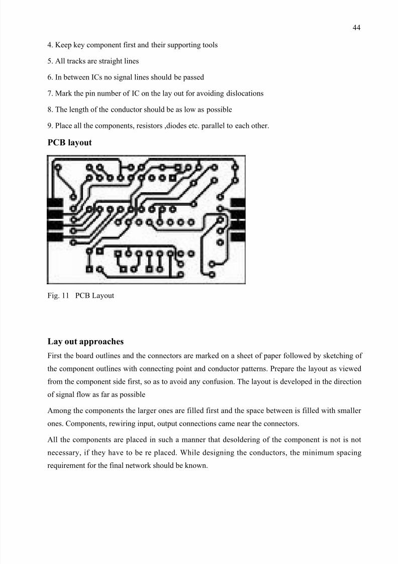
PCB layout
Fig. 11 PCB Layout
Lay out approaches
First the board outlines and the connectors are marked on a sheet of paper followed by sketching of
the component outlines with connecting point and conductor patterns. Prepare the layout as viewed
from the component side first, so as to avoid any confusion. The layout is developed in the direction
of signal flow as far as possible
Among the components the larger ones are filled first and the space between is filled with smaller
ones. Components, rewiring input, output connections came near the connectors.
All the components are placed in such a manner that desoldering of the component is not is not
necessary, if they have to be re placed. While designing the conductors, the minimum spacing
requirement for the final network should be known.
5/13/2018 Main Report - slidepdf.com
http://slidepdf.com/reader/full/main-report-55a7524402170 45/52
45
Transforming the lay out to copper.
The lay out made on the graph sheet should be redrawn on the copper clad using paint or nail polish.
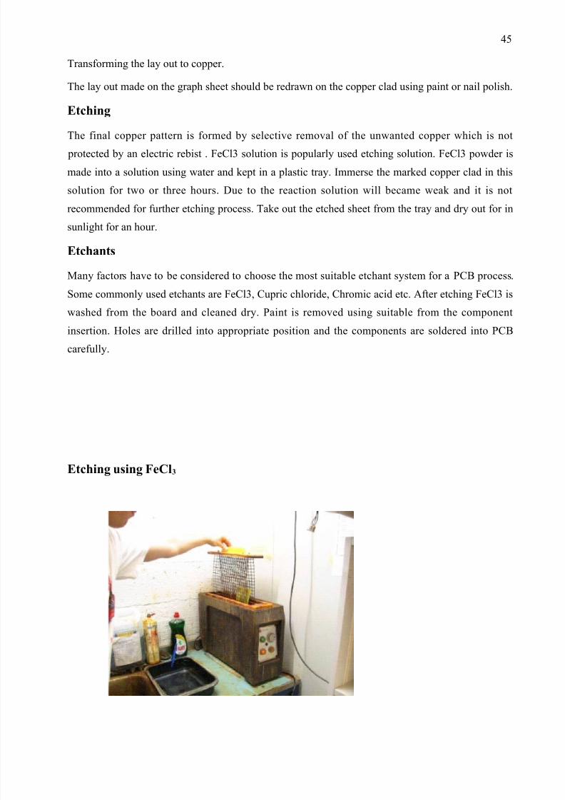
Etching
The final copper pattern is formed by selective removal of the unwanted copper which is not protected by an electric rebist . FeCl3 solution is popularly used etching solution. FeCl3 powder is
made into a solution using water and kept in a plastic tray. Immerse the marked copper clad in this
solution for two or three hours. Due to the reaction solution will became weak and it is not
recommended for further etching process. Take out the etched sheet from the tray and dry out for in
sunlight for an hour.
Etchants
Many factors have to be considered to choose the most suitable etchant system for a PCB process.Some commonly used etchants are FeCl3, Cupric chloride, Chromic acid etc. After etching FeCl3 is
washed from the board and cleaned dry. Paint is removed using suitable from the component
insertion. Holes are drilled into appropriate position and the components are soldered into PCB
carefully.
Etching using FeCl3

5/13/2018 Main Report - slidepdf.com
http://slidepdf.com/reader/full/main-report-55a7524402170 46/52
46
Fig. 12 Etching
Practical implementation
Take a copper clad of the required dimensions. Transfer the circuit layout to the copper clad using
cotton paper. The layout area should be marked with nail polish. Put the copper clad into FeCl3
solution and warm it. Stage by stage transformation of the copper clad occurs. Warm the solution
intermittently according to the requirement. After about 4 hours etching will be completed. Wash the
board using soap solution to remove the remaining of FeCl3 solution. Scrap off the nail polish and
drill holes wherever required using appropriate drill bits. PCB is fabricated.
Fig. 13 Complete PCB
SCOPE OF UTILIZATION
The following advantages could be taken from a Talking Voltmeter
1. Simplicity of installation.
2. The effective ability to be used in labs.
3. It could be used as for measurement of voltage and frequency.
4. Efficient technology for every ECE student.
6. Speakers are used to read out readings.

5/13/2018 Main Report - slidepdf.com
http://slidepdf.com/reader/full/main-report-55a7524402170 47/52
47
BIBLIOGRAPHY & REFRENCES
• www.google.com
• www.yahooanswers.com
• www.wikipedia.com
• www.indipedia.com
• www.engineeringsolutions.com

5/13/2018 Main Report - slidepdf.com
http://slidepdf.com/reader/full/main-report-55a7524402170 48/52
48

5/13/2018 Main Report - slidepdf.com
http://slidepdf.com/reader/full/main-report-55a7524402170 49/52
49
APPENDIX – 1
WORK DISTRIBUTION
In this project we have worked as a team and have divided our work according our different skills
and work interest although we have supported each other for each work. Division of work for each
team member is as follows:
Shobhit Bahri:-
✔ Purchasing of components.
✔ PCB layout making at the lab.
✔ Hardware assembly.
Udita Shah:-
✔ Research work of project and circuit designing.
✔
Report writing for the project.✔ PCB making at the lab.
Tushar Jain:-
✔ PCB making at lab.
✔ Soldering of components.
✔ Mounting of the components.

5/13/2018 Main Report - slidepdf.com
http://slidepdf.com/reader/full/main-report-55a7524402170 50/52
50
Vaibhav Agarwal:-
✔ Purchasing of the components.
✔ Mounting of the components.
✔ Drilling of the PCB.
APPENDIX – 2

5/13/2018 Main Report - slidepdf.com
http://slidepdf.com/reader/full/main-report-55a7524402170 51/52
51
LIST OF COMPONENTS WITH PRICE
11 Resistors
Quantity: References Value Price
10 R1-R6 10k 12/-
10 R8-R11 10k 4/-1 R7 100k 2/-
15 Capacitors
Quantity: References Value Price
7 C1-C3 0.1uF 3/-
C9-C12 0.1uF 4/-
341
C4-C6, C7C5, C13-C15C8
22Uf 1Nf 1uF
2/-1/-1/-
4 Integrated Circuits
Quantity: References Value Price
1 U1 ATMEGA32 250/-
2 U2,U4 7805 26/-
1 U3 7404 25/-
2 Diodes
Quantity: References Value Price11
D1D2
1N40011N4001
2/-2/-
10 Miscellaneous
Quantity: References Value Price
11
J1J2
CONN-H4CONN-H6
4/-6/-

5/13/2018 Main Report - slidepdf.com
http://slidepdf.com/reader/full/main-report-55a7524402170 52/52
52
41111
J3-J6LCDRV1X1Battery
CONN-SIL2LM016L10kCrystal9v
8/-125/-8/-6/-20/-


![Report Main[1]](https://img.pdfslide.net/doc/110x75/551eae364979592e5b8b4770/report-main1.jpg)