Embed Size (px)
Citation preview

HAL Id: tel-02461334https://tel.archives-ouvertes.fr/tel-02461334
Submitted on 30 Jan 2020
HAL is a multi-disciplinary open accessarchive for the deposit and dissemination of sci-entific research documents, whether they are pub-lished or not. The documents may come fromteaching and research institutions in France orabroad, or from public or private research centers.
L’archive ouverte pluridisciplinaire HAL, estdestinée au dépôt et à la diffusion de documentsscientifiques de niveau recherche, publiés ou non,émanant des établissements d’enseignement et derecherche français ou étrangers, des laboratoirespublics ou privés.
Manipulation and detection of spin waves usingspin-orbit interaction in ultrathin perpendicular
anisotropy Ta/FeCoB/MgO waveguidesMathieu-Bhayu Fabre
To cite this version:Mathieu-Bhayu Fabre. Manipulation and detection of spin waves using spin-orbit interaction in ultra-thin perpendicular anisotropy Ta/FeCoB/MgO waveguides. Condensed Matter [cond-mat]. UniversitéGrenoble Alpes, 2019. English. NNT : 2019GREAY028. tel-02461334

THÈSEPour obtenir le grade de
DOCTEUR DE LA COMMUNAUTÉ UNIVERSITÉ GRENOBLE ALPESSpécialité : NANOPHYSIQUEArrêté ministériel : 25 mai 2016
Présentée par
Mathieu-Bhayu FABRE
Thèse dirigée par Ursula EBELS et codirigée par Gilles GAUDIN, CNRS
préparée au sein du Laboratoire Spintronique et Technologie des Composantsdans l'École Doctorale Physique
Manipulation et détection d'ondes de spin via l'interaction spin-orbite dans des guides d'ondes ultraminces Ta/FeCoB/MgO à anisotropie perpendiculaire
Manipulation and detection of spin waves using spin-orbit interaction in ultrathin perpendicular anisotropy Ta/FeCoB/MgO waveguides
Thèse soutenue publiquement le 10 juillet 2019,devant le jury composé de :
Monsieur JOO-VON KIMCHARGE DE RECHERCHE, CNRS ILE-DE-FRANCE-GIF-SUR-YVETTE, RapporteurMonsieur GREGOIRE DE LOUBENSINGENIEUR DE RECHERCHE, CEA DE SACLAY, RapporteurMonsieur DIRK GRUNDLER PROFESSEUR ASSOCIE, ECOLE POLYTECH FEDERALE LAUSANNE -SUISSE, ExaminateurMonsieur OLIVIER FRUCHARTDIRECTEUR DE RECHERCHE, CNRS DELEGATION ALPES, Président


Contents
Introduction 1
1 Theoretical Background 7
1.1 Energy contributions in a thin lm ferromagnetic system . . . . . . . . . . 71.1.1 The exchange energy . . . . . . . . . . . . . . . . . . . . . . . . . . 81.1.2 The dipolar energy . . . . . . . . . . . . . . . . . . . . . . . . . . . 91.1.3 Magnetocrystalline anisotropy energy . . . . . . . . . . . . . . . . . 101.1.4 The Zeeman energy . . . . . . . . . . . . . . . . . . . . . . . . . . 111.1.5 Energy minimization . . . . . . . . . . . . . . . . . . . . . . . . . . 121.1.6 The eective eld . . . . . . . . . . . . . . . . . . . . . . . . . . . . 12
1.2 Uniform magnetization dynamics . . . . . . . . . . . . . . . . . . . . . . . 131.2.1 Equations of motion of the magnetization . . . . . . . . . . . . . . 131.2.2 Polder susceptibility tensor . . . . . . . . . . . . . . . . . . . . . . 151.2.3 Susceptibility for an innite ferromagnetic medium . . . . . . . . . 151.2.4 Susceptibility for a ferromagnetic thin lm . . . . . . . . . . . . . . 171.2.5 Lineshape of the susceptibilities . . . . . . . . . . . . . . . . . . . . 19
1.3 Magnetostatic spin-waves . . . . . . . . . . . . . . . . . . . . . . . . . . . 211.3.1 Spin-waves in the magnetostatic approximation . . . . . . . . . . . 211.3.2 Exchange spin-waves in an innite ferromagnetic medium . . . . . 231.3.3 Exchange spin-waves in a ferromagnetic thin lm . . . . . . . . . . 241.3.4 Relaxation rate . . . . . . . . . . . . . . . . . . . . . . . . . . . . . 27
1.4 Spintronics phenomena . . . . . . . . . . . . . . . . . . . . . . . . . . . . . 271.4.1 The Rashba eect . . . . . . . . . . . . . . . . . . . . . . . . . . . 281.4.2 Spin Hall eects . . . . . . . . . . . . . . . . . . . . . . . . . . . . 301.4.3 Detection of magnetization dynamics via spin pumping and inverse
spin Hall eect . . . . . . . . . . . . . . . . . . . . . . . . . . . . . 321.4.4 Modication of the LLG including the eld-like torque and the
damping-like torque . . . . . . . . . . . . . . . . . . . . . . . . . . 341.4.5 Anisotropic magnetoresistance . . . . . . . . . . . . . . . . . . . . 35
2 Device fabrication 37
2.1 Wafer deposition and annealing . . . . . . . . . . . . . . . . . . . . . . . . 372.2 Device fabrication . . . . . . . . . . . . . . . . . . . . . . . . . . . . . . . 38
i

ii CONTENTS
2.3 Device description . . . . . . . . . . . . . . . . . . . . . . . . . . . . . . . 392.4 Measured samples . . . . . . . . . . . . . . . . . . . . . . . . . . . . . . . 41
3 Spin-orbit torques 43
3.1 Spin-torque resonance technique . . . . . . . . . . . . . . . . . . . . . . . . 433.2 RF Excitation mechanisms . . . . . . . . . . . . . . . . . . . . . . . . . . . 46
3.2.1 Excitation by RF Ørsted eld or RF eld-like torque . . . . . . . . 473.2.2 Excitation by RF damping-like torque . . . . . . . . . . . . . . . . 473.2.3 Inuence of a DC current on resonance conditions . . . . . . . . . 493.2.4 Inuence of the DC damping-like torque on resonance conditions . 49
3.3 Electrical detection of magnetization dynamics . . . . . . . . . . . . . . . 523.3.1 DC signal via to anisotropic magnetoresistance . . . . . . . . . . . 523.3.2 DC signal via spin pumping and inverse spin Hall rectication . . . 563.3.3 Conclusion: AMR vs iSHE . . . . . . . . . . . . . . . . . . . . . . 59
3.4 ST-FMR characterization at zero DC current . . . . . . . . . . . . . . . . 613.4.1 Measurement protocol . . . . . . . . . . . . . . . . . . . . . . . . . 613.4.2 Angle dependence . . . . . . . . . . . . . . . . . . . . . . . . . . . 643.4.3 Saturation magnetization and interfacial anisotropy . . . . . . . . . 643.4.4 Linewidth and damping in the absence of DC current . . . . . . . 69
3.5 ST-FMR characterization with DC current . . . . . . . . . . . . . . . . . . 783.5.1 Shifting of the resonance eld via DC current . . . . . . . . . . . . 803.5.2 Control of the damping via DC current . . . . . . . . . . . . . . . 86
3.6 Conclusion . . . . . . . . . . . . . . . . . . . . . . . . . . . . . . . . . . . . 92
4 Spin-wave excitation and detection 95
4.1 Material and device characterization . . . . . . . . . . . . . . . . . . . . . 954.2 Verication of the dispersion relation . . . . . . . . . . . . . . . . . . . . . 974.3 Excitation of spin-waves via coplanar waveguides . . . . . . . . . . . . . . 98
4.3.1 Magnetic eld generated by a coplanar waveguide . . . . . . . . . . 994.3.2 Spatial prole of spin-waves in a spin-wave waveguide in the Damon-
Eshbach conguration . . . . . . . . . . . . . . . . . . . . . . . . . 1034.3.3 Excitation eciency . . . . . . . . . . . . . . . . . . . . . . . . . . 1044.3.4 Non-zero linewidth model . . . . . . . . . . . . . . . . . . . . . . . 106
4.4 Spin-wave rectication experiments . . . . . . . . . . . . . . . . . . . . . . 1084.4.1 Experimental setup . . . . . . . . . . . . . . . . . . . . . . . . . . . 1084.4.2 Measurement protocol . . . . . . . . . . . . . . . . . . . . . . . . . 1094.4.3 Angle dependence of spin-wave rectication . . . . . . . . . . . . . 1104.4.4 Experimental results . . . . . . . . . . . . . . . . . . . . . . . . . . 111
4.5 Brillouin light scattering experiments . . . . . . . . . . . . . . . . . . . . . 1174.5.1 Working principle . . . . . . . . . . . . . . . . . . . . . . . . . . . . 1184.5.2 Description of the microscope . . . . . . . . . . . . . . . . . . . . . 1184.5.3 BLS measurements . . . . . . . . . . . . . . . . . . . . . . . . . . . 1194.5.4 Spin-wave decay length . . . . . . . . . . . . . . . . . . . . . . . . 121
4.6 Comparison of spin-wave detection methods . . . . . . . . . . . . . . . . . 126

CONTENTS iii
4.7 Conclusion . . . . . . . . . . . . . . . . . . . . . . . . . . . . . . . . . . . . 127
Conclusion and perspectives 129
A Linewidth under a DC damping-like torque 133
Bibliography 133

iv CONTENTS

Introduction
The development of complementary metal-oxide-semiconductor (CMOS) transistorshave long followed Gordon Moore's projection, namely that the density of transistorson a chip doubles every 18 months. However, this sustained exponential growth hasmet serious obstacles. Microelectronics require a variety of memory types that form ahierarchy: the closer the memory is to the processing unit (CPU), the faster it must beto deal with the rapid ux of information. The memory closest to the processor is calledCPU cache and is typically static random-access memory (SRAM). SRAM has accesstimes in the nanosecond range, requires constant voltage to retain information and istypically made up of 6 transistors, which represents a high cost in terms of space. Withtransistor density in modern processors reaching dozens of millions of transistors persquared millimeter, the power consumption and the low density of SRAM represents asignicant technological hurdle, one that is amplied by the current leakage experiencedby nm-sized transistors, leading to heat management issues. One possible solution is theuse of non-volatile, memory to reduce the static power consumption of the CPU cache.A candidate to fulll the requirements of CPU cache is magnetic random-access memory(MRAM), a technology that is at the forefront of a eld of research called spintronics.
Spintronics, a portmanteau of spin electronics, concerns the study of solid state de-vices in which the spin of an electron, in addition to its charge, plays a pivotal role.Historically, the rst development in spintronics was the discovery of tunnel magne-toresistance (TMR) by Jullière in 1975 [Jul75], where the resistance of two ferromagneticlayers separated by an insulator depends on the relative orientation of each ferromagnet'smagnetization. Nowadays, the magnetoresistance of so-called magnetic tunnel junctionsbased on CoFeB/MgO/CoFeB pillars can change by up to several hundreds of % basedon the magnetization state of the two CoFeB layers. However, Jullière's discovery didnot attract too much attention initially, and instead the development of spintronics wasarguably sparked by the discovery of a similar phenomenon called giant magnetoresis-tance (GMR) by Fert and Grunberg in 1986 [Bai88; Bin89] which proved more readilyexploitable using the material deposition techniques available at the time.
Only 11 years after their seminal discovery, IBM commercialized the rst hard diskdrives with giant magnetoresistance read heads. Due to the radical increases in harddrive density made possible by their breakthrough, they were awarded the Nobel prizein physics in 2007. Today, much of the current interest on spintronics lies in the po-tential for scalable, non-volatile memory that can be integrated in CMOS chips. This
1
2 CONTENTS
pursuit was bolstered by the prediction of spin-transfer torque (STT) [Slo96; Ber96]and its subsequent observation [Tso98], where electrons owing in a ferromagnetic layerbecome spin-polarized in the direction of the magnetization, i.e., the proportion of upand down spins are not equal. When passing through a second ferromagnetic layer, theelectrons are re-polarized in the direction of the second layer's magnetization. In ef-fect, the coupled spin-charge current allows the transfer of angular momentum betweenthe two ferromagnetic layers, meaning that one can control the magnetization state ofthe system by injecting a current through the device. Combining spin-transfer torquewith tunnel magnetoresistance, one has the ingredients for an MRAM cell where theinformation is stored in the magnetization state, and a current is used either to read itsstate or to switch it. Such STT-MRAM modules are already commercialized today byEverspin [Mer19], serving as dynamic random-access memory. Modern magnetic tunneljunctions based on CoFeB/MgO/CoFeB are CMOS compatible due to the fact that thematerials can be deposited on a Si wafer by magnetron sputtering, with Ta serving as agrowth layer [Teh99; Gal06; Lin09]. Thus, STT-MRAM can be integrated on top of theprocessing elements [Pre09], instead of adjacent to it, which is the case for SRAM, thussaving space on the integrated circuit and potentially reducing access time. STT-MRAMuses power while reading or writing information but has no static power consumption,in fact memory is retained even when powered o. Sub-nanosecond switching has beendemonstrated [Zha11], fullling the most important requirement of CPU cache: speed.Furthermore, its footprint is small as it requires only a single transistor and the magnetictunnel junction itself, which can scale down to diameters in the nm range [Sai17]. Inaddition, STT-MRAM has the potential to be tailored to compete with other memorytypes: dynamic RAM by being non-volatile, and ash memory by being faster. How-ever the high current required to switch the magnetic state can eventually lead to thebreakdown of the junction, which presents an important hurdle, especially for CPU cacheapplications as writing speeds need to be high, implying high switching currents, and theendurance virtually unlimited.
Developments in spintronics in the last decade have led to the resurgence of twophenomena discovered in the 1970s which have helped overcome this obstacle: the Rashbaeect [Ohk74; Byc84] and the spin Hall eect [Dya71b; Dya71a], both of which were rstpredicted for semiconductors or 2D electron gases. When they were discovered to bepresent in normal metals [Mir10; Mir11], it opened a new research eld called spin-orbitronics. The aforementioned phenomena allow the creation of so-called spin-orbittorques (SOT) that are generated by a charge current in a normal metal, leading to newapproaches for exciting the magnetization of an adjacent ferromagnet. The materialsused to generate these eects include heavy metals such as Pt, Ta or W, owing to theirlarge atomic number and thus large spin-orbit coupling. Ta and W have the advantageof being compatible with CoFeB/MgO/CoFeB magnetic tunnel junctions, retaining theircompatibility with CMOS chips. Thus, a new class of devices emerged, called SOT-MRAM, which has the benet of separating the reading current from the writing current,resulting in increased reliability and endurance [Pre16; Gar18], while still demonstratingsub-nanosecond switching times [Cub18].

CONTENTS 3
Spintronics show the potential to disrupt conventional electronics in even more radi-cal ways. The reduction of the transistor gate size has led to the static power dissipatedby leakage has reached the same order of magnitude as the active power consumption[Jeo10]. This is due to the fact that energy, or information, in conventional electronicsis physically manifested by currents and voltages, which, in nm-sized transistor gatesinevitably leads to losses via switching or leakage by electron tunneling. In spintronics,information is mediated by spin moments, which can propagate without a net ow ofcharges. This propagation of spin currents can occur via spin-waves, the collective motionof local magnetic moments in a ferromagnetic or antiferromagnetic medium. Addition-ally, their wave-like nature allows wave-based logic in which information is encoded inthe amplitude or the phase of the spin-wave. Proof-of-concept devices include a varietyof logic gates (AND gate, XOR gate, etc.) [Sch08; Khi11; Nik15], majority gates [Kli14],magnon transistors [Chu14], spin-wave multiplexer [Vog14], spin-wave couplers [Sad15a]and beam splitter [Sad15b].1 Some of these devices require less components than theirsemiconductor equivalents and thus, if they can be miniaturized successfully, they couldhave smaller footprints or consume less power. Thus, the study of spin-waves, a eldcalled magnonics,2 shows potential for the propagation as well as the processing of in-formation with small footprints and low power consumption. Combined with MRAMcache, memory and storage, one can even envision all-magnetic processors.
One of the most ubiquitous materials studied for magnonics is the yttrium iron garnet(YIG), a ferrimagnetic insulator in which spin-waves can propagate distances on the orderof cm thanks to its damping parameter in the 10−5 range, which is the lowest of all knownmaterials [Che93]. Even though there is much research activity on growing YIG thin lmsand creating YIG microstructures [Ham14], including all of the proof-of-concepts citedearlier, a signicant problem lies in its inherent incompatibility with CMOS, due to thefact that YIG is grown via liquid phase epitaxy [Gla76; Sho85] or pulsed laser deposition[Dor93; Sun12], on a specic substrate: gadolinium gallium garnet. Thus, there is alsosignicant interest in CMOS-compatible material systems such as metallic NiFe alloys3
[Bai03; Sch08; Dem09] and CoFeB alloys4 [Con13; Ran17] as well as half-metallic Co-based Heusler compounds [Seb12; Pir14]. However these materials have larger dampingparameters in the 10−3 range and thus the spin-wave propagation distances are only onthe order of µm.
For magnonic devices to compete with conventional electronics, they must be CMOS-compatible, scalable into the nanometer range and accordingly use spin-waves with wave-lengths in the same range. This requires the development of materials and microstruc-tures in which such spin-waves can propagate far enough to be of use, as well as integrated
1For a review on magnonic devices, see [Chu17].2From the wave-particle equivalence picture, a quantized spin-wave is a quasiparticle called a magnon,
leading to the name of the eld of research.3NiFe alloys studied in spintronics and magnonics usually have one of the following compositions:
Ni80Fe20 or Ni81Fe19. These alloys are often called permalloy, abbreviated as Py.4There are many dierent studied CoFeB alloys including Co60Fe20B20, Co20Fe40B20, Co20Fe60B20.
The Fe-rich alloy used in this work is rather specic to the Spintec laboratory and is referred to as eitherFe72Co8B20 or FeCoB here.

4 CONTENTS
methods to generate, interact with, and detect these spin-waves on-chip. Moreover, dueto the need for nm-sized devices, the disadvantage of metallic systems with high dampingand low propagation length is less important.
Much like phonons, non-coherent magnons spontaneously appear in ferromagneticmaterials at non-zero temperature. However, magnonics often involves the study ofcoherent, non-thermal spin-waves, thus requiring methods for exciting spin-waves withhigher energy. The simplest method involves driving an RF current in the GHz rangeinto an antenna near the ferromagnetic material, thereby exciting via the Ørsted elda range of spin-waves dictated by the conductor's geometry [Ols67]. The techniquewas further rened by using microstructured antennae such as microstrips [Gan75] andcoplanar waveguides [Bai03]. Spin torques can also be used to excite spin-waves, thoughthey are not wavevector selective, meaning that they excite a broad range of spin-wavesincluding thermal spin-waves [Dem11]. Coherent spin-wave excitation can be obtainedby using a point contact geometry, through which a spin-polarized current is injectedinto a ferromagnetic layer to generate localized spin-waves [Ji03; Sla05]. Alternatively,by patterning a FM/NM layer (ferromagnetic/normal metal with spin-orbit interactionsuch as NiFe/Pt) into a nanoconstriction [Dem14; Che16] or other restrictive shapes[Dua14], thereby modifying the local demagnetizing eld, SOTs can excite a single spin-wave mode, the so-called localized spin-wave bullet. These are non-propagating spin-waves, and thus of limited interest for spin-wave based logic, though Madami et al.observed out-of-plane spin-waves excited locally by STT propagate into the ferromagneticmedium [Mad11]. Novel techniques include femto-second lasers [Iih16] or the use ofan RF localized electric eld to modify the perpendicular magnetic anisotropy of theCoFeB/MgO interface [Ran17].
Another obstacle for the integration of spin-wave based devices onto CMOS integratedcircuits is the detection of the spin-waves themselves. Detection methods include largeand expensive ex situ equipment such as Brillouin light scattering spectroscopy [Seb15;Dem15] and magneto-optical Kerr eect microscopy [Par02], as well as propagating spin-wave spectroscopy [Bai03]. The rst two are laboratory equipments and in no wayintegrable onto a chip. The last is based on waveguides for the inductive detection ofspin-waves, which has its own drawbacks, owing to the fact that the inductive couplingis wavevector-dependent. The reciprocal of the spin Hall eect, called the inverse spinHall eect (iSHE), has been shown to be able to detect spin-wave dynamics in Pt/NiFesystems [And09] and YIG/Pt [Hah13], and only requires that a metal with high spin-orbit coupling be adjacent to the material in which the spin-waves propagate, makingthe inverse spin Hall eect a promising detection method for scalable integration.
This thesis addresses the development of scalable CMOS-compatible spin-wave de-vices by investigating the properties of a spin-wave waveguide based on an ultrathinTa/FeCoB/MgO wire. The material system was chosen for its compatibility with CMOSprocesses, the perpendicular anisotropy arising from the FeCoB/MgO interface [Cuc15]and strong spin-orbit interactions in the Ta and at the Ta/FeCoB interface [Cub18]. Thepurpose of the spin-orbit interactions is twofold: rstly, to allow the manipulation ofspin-waves via spin-orbit torques [Dem11], secondly, to allow the detection of magneti-

CONTENTS 5
zation dynamics via the combined eects of spin-pumping and the iSHE [And09]. Forthe excitation of spin-waves, we designed nanometric coplanar waveguides on top of theSWWs capable of exciting a large range of non-zero wavevectors. This thesis is organizedas follows:
The rst chapter gives an overview of the theory needed to understand the experi-ments described in this thesis. The dierent energy contributions present in a magneticsystem are introduced, and the Landau-Lifshitz equation, which governs magnetizationdynamics, is given. Subsequently, we calculate the susceptibility tensor for a variety ofsystems, successively adding terms such as the shape anisotropy, perpendicular magneticanisotropy, and damping. Similarly, we introduce spin-waves and give the frequency-wavevector dispersion relation for several systems. The last section concerns spin-orbitinteractions such as the Rashba eect and the spin Hall eect, which can interact withthe magnetization dynamics via the eld-like torque and the damping-like torque; as wellas the inverse spin Hall eect and anisotropic magnetoresistance, which can be used todetect magnetization dynamics.
In the second chapter we briey describe the cleanroom fabrication process of thespin-wave waveguides and the coplanar waveguides, and give a detailed description ofthe devices.
The third chapter concerns ST-FMR experiments. We derive the rectied voltagesthat may arise from the dierent potential sources of rectication and then determinemagnetic properties of Ta/FeCoB/MgO as a function of the FeCoB thickness. Doingso, we identify the ferromagnetic layer thickness for which the magnetization transitionsfrom in-plane to out-of-plane, and focus on devices with a thickness around and at thetransition. Subsequently, by performing a DC current-dependent study, we characterizethe eld-like and damping-like torques as a function of the ferromagnetic thickness aswell.
The fourth chapter deals with the excitation of spin-waves and their detection viathe inverse spin Hall eect. First we give the expected spin-wave spectrum excitedby an RF current injected in nanometric coplanar waveguides, taking into account theperpendicular magnetic anisotropy and the non-zero linewidth of the spin-waves. Wethen perform SWR spectroscopy. Similarly to ST-FMR, the spin-wave dynamics leads toa rectied signal that can be detected electrically via the iSHE. Afterwards we comparethese results to Brillouin light scattering microscopy performed on the same type ofdevices. The BLS experiments also allow us to characterize the spin-wave decay lengthand lifetime in systems with perpendicular magnetic anisotropy.
Finally, a brief summary of the ndings is presented at the end of this thesis, and aperspective for scalable, integrated magnonics-spin-orbitronics is given.

6 CONTENTS

Chapter 1
Theoretical Background
This chapter gives an overview of the theoretical background necessary to understandthe experimental studies presented in this thesis. In order to characterize the spin-orbittorques' eects in Ta/FeCoB/MgO structures, we excite ferromagnetic resonance andspin-waves via a high frequency Ørsted eld or spin-orbit torque, and we detect themagnetization dynamics by the combined eects of spin-pumping and the inverse spinHall eect.
Therefore, in this chapter we introduce the underlying physical phenomena of mag-netization dynamics, spin-orbit torques, spin-pumping, and the inverse spin Hall eect.For the magnetization dynamics, we present the dierent energies that arise in a ferro-magnetic system, and how they contribute to the equilibrium magnetization. Next, weprovide the equation that governs the dynamics of the magnetization, and from it, de-rive the Polder susceptibility tensor, which gives the uniform magnetization's responseto a high frequency excitation. This is done for several cases, from the innite ferro-magnet to the thin lm with perpendicular anisotropy. We then address the formalismfor non-uniform magnetization dynamics, known as spin-waves, and derive the linearspin-wave dispersion relation for several ferromagnetic systems. Next, we present thespin-orbit phenomena that allow the control of the magnetization dynamics, specicallythe Rashba eect and the spin Hall eect, and the two torques that arise: the eld-liketorque and the damping-like torque. We also discuss the inverse spin Hall eect, which,coupled with spin-pumping, is used for the detection of magnetization dynamics in thedevices studied in my thesis. The nal subsection deals with anisotropic magnetoresis-tance, a further spin-orbit eect present in ferromagnetic materials that can also be usedfor probing the magnetization's state.
1.1 Energy contributions in a thin lm ferromagnetic sys-tem
The internal energy of a ferromagnetic system such as the Ta/FeCoB/MgO systemconsidered in this work is, among others, the sum of the exchange energy, the Zeeman
7

8 CHAPTER 1. THEORETICAL BACKGROUND
energy, the magnetocrystalline anisotropy energy and the dipolar energy of the ferro-magnetic material. In this section we describe each energy involved and their origin for aferromagnetic material. The case of the ferromagnetic thin lm, where the thickness is inthe nanometer range and the lateral dimensions are several orders of magnitude larger,will be considered.
1.1.1 The exchange energy
The exchange interaction is a purely quantum mechanical eect which arises as a con-sequence of the Pauli exclusion principle and the fact that electrons are indistinguishablein a solid. It is responsible for the spontaneous ordering of spins within ferromagneticand antiferromagnetic materials. The Heisenberg model [Hei28], a derivation of whichcan be found in English in [Stö06], describes the exchange energy between an atom jwith spin Sj and all other atoms i with spin Si in a crystal. A simplied form consists ofconsidering only the nearest neighbors' interaction (symbolized by nn in the equation)in the summation [OHa99]:
Eex,j = −2
nn∑i<j
JijSi · Sj (1.1)
where Jij , expressed in units of Joules, is the exchange constant for the considered spins.It is positive for ferromagnets (favoring parallel alignment of spins) and negative for anti-ferromagnets (favoring anti-parallel alignment). The exchange interaction is strongerthan any other interaction considered in this section, but its range is very small, suchthat one can simply consider the interaction between an atom j and only its nearestneighbors. In the continuum approach, one can derive an expression of the energy forcontinuous media [OHa99], yielding an exchange energy for the local magnetizationM(r)at the coordinate r that is written:
Eex =
∫V
AexM2s
((∂M(r)
∂x
)2
+
(∂M(r)
∂y
)2
+
(∂M(r)
∂z
)2)d3r (1.2)
where Ms = |M| is the saturation magnetization of the considered magnetic material(in A m−1) and Aex is the exchange stiness constant (in J m−1), which is a macro-scopic measure of the stiness of coupling of the spins. While the exchange energy is thedominant term for magnetic ordering at the atomic scale, it is too short-ranged to beresponsible for the formation of magnetic domains or hysteretic behavior. For a uniformmagnetization, the exchange energy is minimal and the exchange interaction doesn't ap-pear in magnetostatics or magnetization dynamics. However, it can have a signicantrole in the boundary between two magnetic domains, called domain walls; and the prop-agation of perturbations in the magnetic ordering, called spin-waves; in both cases, themagnetization deviates from a uniform parallel alignment.
1.1. ENERGY CONTRIBUTIONS IN A THIN FILM FERROMAGNETIC SYSTEM9
1.1.2 The dipolar energy
The dipolar energy, also called magnetostatic or demagnetizing energy, arises fromthe dipole-dipole interaction between magnetic moments. In contrast to the exchangeinteraction, the dipolar interaction is weak but long-ranged, such that for nite systemsits analytical calculation is complex and its computation in micromagnetic simulationstime-consuming. The magnetic eld created by a magnetic dipole µj at a position r is:
Hj(r) =1
4π
(3r(r · µj)
r5−
µj
r3
)(1.3)
where r = |r|. The dipolar energy is the sum of the energy arising from the dipolar inter-action between all of the moments. For an innite magnetic medium, these interactionscancel each other out if the magnetization is uniform. For nite solids, the magneticmoments do not compensate each other at the boundary surfaces, resulting in dipolarelds. Inside the ferromagnet, these are referred to as demagnetizing elds, while outsideof it they are called stray elds.
Accounting for all the magnetic moments in a solid, the volumetric energy of thedipolar eld Hd is given by [Mor01]:
EdV
= − µ0
2V
∫VHd(r) ·M(r)d3r =
µ0
2V
∫∞Hd
2(r)d3r (1.4)
where V is the volume of the ferromagnetic solid and µ0 is the vacuum permeability.1 Therst expression indicates that the energy is localized in the magnetic volume. Howeverthe equivalent second expression is obtained by considering the energy of the dipolareld created by the ferromagnet, distributed throughout space [Mor01]. It shows thatthe dipolar energy is always positive and that the greater the stray elds, the greaterthe energy, which is unfavorable. As a consequence, in ferromagnets where the dipolarinteraction is dominant, the magnetization at the edges of a solid will favor aligningparallel to the edges, minimizing the stray elds. In the case of a thin rectangular wire,the magnetization will tend to align with in-plane and parallel to the long axis of therectangle. This behavior of the magnetization, which favors a particular direction in thesolid to minimize the dipolar energy, is referred to as shape anisotropy, and can result inthe hysteretic behavior of ferromagnets. On the other hand, for an innite ferromagneticmedium, there is no shape and thus no shape anisotropy.
In the case of a uniform magnetizationM, the expression of the dipolar energy densitycan be simplied to:
ed =µ0
2MT ·N ·M (1.5)
where MT is the transpose of the magnetization vector and N is the demagnetizingtensor, a set of parameters dependent on the geometry of the magnetic volume. Itsexpression can be found in [New93]. However its analytical calculation is non-trivial
1µ0 = 4πe−7 ≈ 1.2566 × 10⁻⁶ T m A−1.

10 CHAPTER 1. THEORETICAL BACKGROUND
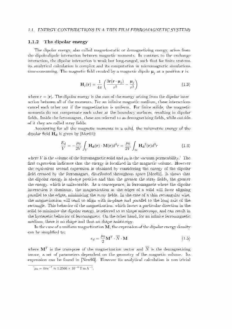
for many geometries, such that developing ecient and accurate approximations is aconcern for micromagnetic simulations. The tensor can be diagonalized, and it can beshown that its trace is equal to one [New93]. For a thin lm with a uniform magnetizationand lateral dimensions much greater than the thickness, a sucient approximation forthe demagnetizing tensor is to consider only one non-zero coecient, Nxx = 1, with xthe growth direction of the thin lm, perpendicular to the thin lm plane (see Fig. 1.1).The demagnetization energy density becomes:
ed =µ0
2(M · x)2 (1.6)
Thus, the dipolar energy in thin lms is minimized when the magnetization lies in thethin lm plane. Formulas and tables for demagnetizing tensor components have beencalculated for dierent geometries, such as ellipsoids [Osb45], cylinders [Boz42] and slabs[Jos65].
Figure 1.1: Coordinate system for describing resonance in a Ta/FeCoB/MgO spin-wavewaveguide. The x axis is perpendicular to the lm plane and the z axis is parallel to theexternal magnetic eldH. The magnetization is saturated by the eld and its equilibriummagnetization Meq is also parallel to z.
1.1.3 Magnetocrystalline anisotropy energy
In crystalline ferromagnetic media, an energy contribution appears due to electronorbitals coupling with the lattice and with the spin moments, the magnetocrystallineanisotropy energy. This gives rise to preferential magnetization directions that are oftenalong crystalline axes and contribute to the hysteretic behavior of ferromagnets. Inmaterials such as hcp (0001) Co [Heh96], there is one preferential direction called theeasy axis, and the anisotropy is called magnetocrystalline uniaxial anisotropy. The energydensity for a magnetization M is:
emc = Ku
(1−
(M
Ms· k)2)
(1.7)
where Ku is the uniaxial anisotropy constant (in J m−3), and k is the direction of theeasy axis.

1.1. ENERGY CONTRIBUTIONS IN A THIN FILM FERROMAGNETIC SYSTEM11
The material system used in this work is a thin lm stack deposited on a silicon waferby magnetron sputtering, starting from the silicon substrate: Ta, Fe72Co8B20 (hereafterreferred to as FeCoB) and Mg. The sample is then oxidized and annealed. As a result, thematerial is polycrystalline in nature, but the distribution of the crystalline orientationsis not random, instead the grains show a preferential growth direction. Such a materialis said to be textured [Tak07], but the resulting magnetocrystalline uniaxial anisotropyis negligible in such materials.
However another source of magnetocrystalline anisotropy can appear in such a mate-rial system. The electronic environment of the atoms at the interface of the ferromagneticlayer has reduced symmetry compared to those in the volume which modies the atomicorbitals and can lead to a magnetic anisotropy perpendicular to the plane. In the pres-ence of a metallic oxyde such as MgO the perpendicular anisotropy is further increased,which is attributed to the hybridization of oxygen and transition metal orbitals [Yan11].Experimentally, the anisotropy can be tuned by the oxydation and annealing conditions[Mon02; Rod09]. Both phenomena occur at the interface between FeCoB and MgO, giv-ing rise to a magnetocrystalline anisotropy that favors a magnetization along the growthaxis. It is called perpendicular magnetic anisotropy (PMA), surface anisotropy or inter-facial anisotropy. For a ferromagnetic thin lm with a uniform magnetization M, theenergy density of PMA for a ferromagnetic layer of thickness tf is:
emc =Ki
tf
(1−
(M
Ms· x)2)
(1.8)
where x is the growth axis and the normal to the interface and Ki is the interfacialanisotropy constant for the ferromagnet/oxide interface (in J m−2). The PMA energy isminimum when the magnetization is either parallel or anti-parallel to the growth axis.Due to the thickness dependence, the anisotropy can be extremely high for thin lms inthe nanometer range, such that it overcomes the demagnetization energy and reorientsthe magnetization perpendicular.
1.1.4 The Zeeman energy
The Zeeman energy is the potential energy of a ferromagnetic solid subjected to anexternal magnetic eld. The moments in the solid will tend to align with the eld tominimize the energy. For a magnetization M in a eld H, the energy density is:
eZ = −µ0M ·H (1.9)
It is minimum when the magnetization is aligned parallel with the eld. In contrastto the interactions in previous sections, the Zeeman energy favors a single direction forthe magnetization for ferromagnetic materials. In the work presented here, the staticexternal eld is always in the plane of the thin lm.

12 CHAPTER 1. THEORETICAL BACKGROUND
1.1.5 Energy minimization
The ferromagnetic system reaches an equilibrium state when the energy is minimized.The mechanisms of how this equilibrium is reached is described in Sec. 1.2.1. The totalinternal energy density e is the sum of the energy densities seen in the previous sections:
e = eex + ed + emc + eZ (1.10)
As the interactions responsible for these energies compete with each other, the equi-librium state can be a state where none of the energies are individually minimized. Itis represented by the magnetization M, which can be uniform, split into domains, orpresent complex structures such as vortices.
For thin lms, materials can be referred to as in-plane magnetized, i.e., the magne-tization lies in the plane in the absence of an external eld, or as out-of-plane, i.e., theequilibrium position is normal to the plane; there are also cases where the magnetizationis oriented in an intermediate direction. When the magnetic system has PMA, there isa critical thickness tc, dened further below, where the magnetization reorients from thein-plane to the out-of-plane direction
1.1.6 The eective eld
To include the dierent interactions described in the previous section into an equationdescribing the dynamics of the magnetization, it is useful to express the interactions inthe form of an eective eld. For each energy density ei dened above, where i =ex, d,mc, Z, one can dene the corresponding eective eld Hi
eff :
Hieff = − 1
µ0
∂ei∂Mx∂ei∂My∂ei∂Mz
= − 1
µ0
∂ei∂M
Heff =∑i
Hieff = − 1
µ0
∂e
∂M
(1.11)
The total eective eld Heff is the local eld felt by the magnetization, the eld alongwhich the magnetization will align if there is damping, through mechanisms detailedin the next section. The eective elds for the interactions described in the previoussections, assuming the presence of interfacial anisotropy, are:
Heff =2Aexµ0M2
s
∇2M(r) + M(r) · x(
2Ki
µ0M2s tf− 1
)x + H (1.12)
where ∇2 is the vector Laplace operator, which, in Cartesian coordinates, is written forM(r):
∇2M(r) =
∇2Mx(r)∇2My(r)∇2Mz(r)
(1.13)

1.2. UNIFORM MAGNETIZATION DYNAMICS 13
The right side of Eq. (1.12) contains the exchange eld, the anisotropy eld, the de-magnetizing eld and the external eld. In the case of a uniform magnetization, theexchange eld is zero. The demagnetizing and interfacial anisotropy elds depend on thesame component of the magnetization and directly compete with each other: the formerbrings the magnetization into the plane, while the latter tries to pull it out of the plane.It is often useful to dene an eective magnetization that sums up their eect:
Meff = Ms −2Ki
µ0Mstf(1.14)
Thus, the sign of the eective magnetization gives the dening behavior of the materialin the absence of an external eld: in-plane ferromagnetic thin lms haveMeff > 0 whileout-of-plane ferromagnetic thin lms have Meff < 0, and Meff = 0 denes the criticalthickness tc of the reorientation from in- to out-of-plane, given by:
tc =2Ki
µ0M2s
(1.15)
1.2 Uniform magnetization dynamics
1.2.1 Equations of motion of the magnetization
Now that we have dened the eective eld, we can describe the behavior of themagnetization when it experiences small perturbations. The equation of motion of themagnetization in response to a perturbation is given by the eective eld Heff :
dM
dt= −γµ0M×Heff (1.16)
where γ is the gyromagnetic ratio dened by:
γ =|e|g2me
= 1.84× 10¹¹ rad s−1 T−1
γ′ =γ
2π= 29.25 GHz T−1
(1.17)
where e and me are the electron's charge (in Coulomb) and its mass (in kg), and g isthe unitless Landé g-factor.2 Eq. (1.16), which is also called the lossless Landau-Lifshitzequation, describes the precessional motion of the magnetization around the eectiveeld at an angular frequency γµ0Heff . Additionally, since the eective eld depends onthe magnetization, the eld's direction and magnitude can change as the magnetizationprecesses around it.
Eq. (1.16) does not accurately describe the magnetization dynamics because it de-scribes only the precession of the magnetization around its equilibrium but not the losses
2The value used in this work is the value found for bulk Fe g = 2.09 found in [Dev13].

14 CHAPTER 1. THEORETICAL BACKGROUND
that are needed to bring the magnetization back to its equilibrium parallel to the eec-tive eld. Experimentally, applying a magnetic eld on a ferromagnet will result in themagnetization taking a damped, swirling trajectory around the eld, until it is alignedparallel to it. Phenomenologically, this can be described by the ansatz used by Landauand Lifshitz [Lan35], in what is now referred to as the Landau-Lifshitz (LL) equation:
dM
dt= −γµ0M×Heff −
α′γµ0
Ms(M× (M×Heff )) (1.18)
where the last term describes a dissipative torque that leads to the magnetization aligningparallel with the eld, with α′ being a dimensionless damping parameter. The dampedprecessional motion is illustrated in Fig. 1.2.
Figure 1.2: Motion of the magnetization M due to an eective eld Heff in the presenceof damping. The precessional term (green) makes the magnetization turn around theeective eld while the damping term (yellow) reduces the angle of the cone of precessionuntil the magnetization is aligned with the eective eld.
However later experiments by Gilbert and Kelly showed that the LL equation couldnot adequately predict the high damping factors or times scales of relaxation they mea-sured. The Landau-Lifshitz-Gilbert (LLG) equation was then proposed in 1955 [Gil55]to accurately model materials with high damping:
dM
dt= −γµ0M×Heff +
α
Ms
(M× dM
dt
)(1.19)
It is possible to transform the LLG into an equation of the same form as the LL byinjecting the expression of dMdt back into the LLG itself:
dM
dt= − γµ0
1 + α2M×Heff −
α′γµ0
Ms (1 + α′2)(M× (M×Heff )) (1.20)
The subtle dierence between the two equations and the two dampings is a long standingdebate in the literature. However, even for rather large damping α = 0.1, we only have1 + α2 ≈ 1.01. Thus, in the analytical calculations described in this work, this factor

1.2. UNIFORM MAGNETIZATION DYNAMICS 15
will be neglected and we will consider the LL and the LLG equations to be equivalent,and the damping parameters equal α = α′. In simulations, it is advantageous to use theLL equation or the LLG equation as written in Eq. (1.20) since the time derivative ofthe magnetization appears only on the left side of the equation, allowing for algorithmsto solve the dierential equation such as the predictor-corrector method used in theOOMMF micromagnetic simulation program.3
Dissipation mechanisms
The dissipation of angular momentum in magnetization dynamics can have intrin-sic [Hic09] and extrinsic origins. The latter includes impurities [Nem11], two-magnonscattering [Hei85; Lin03] and spin pumping [Tse02a]. It was initially assumed in thiswork that there are only damping processes of the viscous or Gilbert-type, such that itcan be described by α in the LL or LLG equations. However, in Sec. 3.4.4, we presentsignatures of non-Gilbert-type damping for the system studied here, Ta/FeCoB/MgO,related to inhomogeneities.
1.2.2 Polder susceptibility tensor
The Polder susceptibility tensor χ describes the dynamic response of the magneti-zation of a ferromagnetic system to an external alternating eld. The susceptibility isdened by the following relation:
M = χh (1.21)
where h is the excitation RF magnetic eld. In the following section, the susceptibilitytensor will be calculated for dierent geometrical and material considerations.
1.2.3 Susceptibility for an innite ferromagnetic medium
Let us linearize the lossless equation of motion Eq. (1.16) by evaluating small-angledisplacements of the magnetization M of an unbounded ferromagnet under the eectof a static external magnetic eld H applied along z. Since the ferromagnet is innite,and the magnetization is considered uniform, there is no demagnetizing eld and nointerfacial anisotropy. The magnetization at equilibrium Meq is saturated and is alignedwith H. If we now consider that the magnetization is slightly tilted out of equilibrium,and apply a time dependent magnetic eld h in the xy plane, then the magnetizationwill precess around the applied eld and we can write:
M = Meq + m
Heff = H + h(1.22)
where h H and m Meq, such that Meq ≈ Ms. The term m is the dynamiccomponent of the magnetization that rotates in the xy plane around the applied eld H,
3The Object Oriented MicroMagnetic Framework (OOMMF) project at ITL/NIST. For more infor-mation, see: https://math.nist.gov/oommf/.

16 CHAPTER 1. THEORETICAL BACKGROUND
while Meq is constant. Similarly, Heff is split into the static eld H and the dynamiceld h. Substituting Eqs. (1.22) into Eq. (1.16), we obtain:
dM
dt= −γµ0 (Meq ×H + Meq × h + m×H + m× h) (1.23)
Since the magnetization at equilibrium is considered to be aligned with the static eld,the rst term on the right side is zero, and the last term is of second order and thereforeneglected. We then obtain the linearized equation of motion for an undamped, innite,ferromagnetic medium:
dm
dt= −γµ0 (Meq × h + m×H) (1.24)
Assuming that the time dependent eld and the dynamic component of the magnetizationhave the same time dependence eiωt, Eq. (1.24) can be rewritten:
iωm = −z× (ωMh− ωHm) (1.25)
where the saturation magnetization and static eld are written in terms of angular fre-quencies:
ωM = γµ0Ms
ωH = γµ0H(1.26)
Assuming that the dynamic components of the magnetization and eld along the z axisare negligible, we solve Eq. (1.25) for h in two dimensions:(
hxhy
)=
1
ωM
(ωH −iωiω ωH
)(mx
my
)(1.27)
where hi and mi are the components of h and m respectively. The inverse of the Poldersusceptibility tensor dened by Eq. (1.21) can be recognized:
h = χ−1
m (1.28)
whereM can be substituted bym since we are only interested in the dynamic component.Inverting the matrix, we obtain the Polder susceptibility tensor and its components:
χ =
(χ‖ iχ⊥−iχ⊥ χ‖
) χ‖ =ωHωMω2H − ω2
χ⊥ =ωωM
ω2H − ω2
(1.29)
As ω → ωH , the magnetization enters resonance, which is translated by the elements ofχ diverging. This frequency is called the ferromagnetic resonance frequency (FMR). Inthe next sections, the LL equation and the eective eld will be modied to take intoaccount additional interactions, yielding dierent expressions for the components of thesusceptibility tensor.

1.2. UNIFORM MAGNETIZATION DYNAMICS 17
1.2.4 Susceptibility for a ferromagnetic thin lm
For bounded systems, the dipolar energy is non-zero and adds a term in the eectiveeld that is dependent on the magnetization. For in-plane magnetized thin lms with xnormal to the lm plane, the total eective eld becomes:
Heff = H + h− (m · x) x (1.30)
where the last term is the demagnetization eld, and where the static eld H is stillapplied along the z axis and the dynamic eld h is in the xy plane. For the demagnetiza-tion term, only m remains since the magnetization is still saturated and M is parallel toz. Injecting the above into Eq. (1.16) and once again neglecting the products of secondorder, we obtain: (
hxhy
)=
1
ωM
(ωH + ωM −iω
iω ωH
)(mx
my
)(1.31)
Inverting Eq. (1.31) yields the susceptibility components:
χ =
(χxx iχxy−iχxy χyy
) χxx =ωHωMω2
0 − ω2
χxy =ωωMω2
0 − ω2
χyy =ωM (ωH + ωM )
ω20 − ω2
(1.32)
where:ω2
0 = ωH (ωH + ωM ) (1.33)
is the square of the ferromagnetic resonance angular frequency for the thin lm. Theequation for the FMR frequency ω0 of a ferromagnet is known as the Kittel formula; anumber of geometric congurations can be found in [Kit48]. Compared to the bulk, thethin lm reduces the symmetry of the system, which results in the diagonal componentsof the tensor being no longer equal.
With interfacial anisotropy
As seen in Sec. 1.1.6, interfacial anisotropy directly competes with the dipolar inter-action in thin lm stacks. The eective eld becomes:
Heff = H + h + (m · x)
(2Ki
µ0M2s tf− 1
)x (1.34)
In the case of in-plane magnetized samples, the equilibrium magnetization will align withthe static eld. However for out-of-plane magnetized samples, the static eld must bestrong enough so that Meq becomes aligned with H in the plane, so that the derivationof the susceptibility in the previous sections is still valid. Injecting the equation aboveinto Eq. (1.16) and solving for h yields:(
hxhy
)=
1
ωM
(ωH + ωM − ωK −iω
iω ωH
)(mx
my
)(1.35)

18 CHAPTER 1. THEORETICAL BACKGROUND
The components of the Polder tensor are then:
χxx =ωHωMω2
0 − ω2
χxy =ωωMω2
0 − ω2
χyy =ωM (ωH + ωM − ωK)
ω20 − ω2
(1.36)
where the anisotropy eld is expressed in terms of angular frequency:
ωK = γ2Ki
Mstf(1.37)
and the resonance frequency is dened by:
ω20 = ωH (ωH + ωM − ωK) (1.38)
Thus the interfacial anisotropy introduces a thickness dependence, and for a given ap-plied eld, reduces the resonance frequency. The dependence of the resonance frequencyon ωM − ωK = µ0γMeff makes it impossible to disentangle the contribution of the de-magnetizing eld and of the anisotropy eld from a single FMR experiment for a xedferromagnetic layer thickness. Only the eective magnetization Meff can be obtainedfrom a single measurement. To disentangle Ki and Ms it is necessary to do a thicknessdependent study as will be shown in Chap. 3.
With damping
The equation of motion used so far in this section to describe the magnetizationdynamics does not take into account the dissipation of angular momentum. The LLGequation provides a convenient way of deriving the susceptibility in lossy ferromagneticmedia. Rewritting Eq. (1.19) using the same separation of static and dynamic compo-nents as in Eq. (1.23), and neglecting products of second order, we obtain:
dm
dt= −γµ0 (Meq × h + m×H) +
α
Ms
((Meq + m)× dm
dt
)(1.39)
Assuming the same time dependence eiωt for the applied dynamic eld and the dynamicmagnetizations, we can write:
iωm = −z× (ωMh− ωHm) +α
Ms((Meq + m)× iωm)
≈ −z× (ωMh− (ωH + iαω)m)(1.40)
Thus, including the damping term is equivalent to making the substitution ωH → ωH +iαω. For a thin lm including a demagnetizing eld, without interfacial anisotropy, the

1.2. UNIFORM MAGNETIZATION DYNAMICS 19
Polder susceptibility tensor's components are:
χxx =ωMωH
ω20 − ω2 + iαω(ωM + 2ωH)
χxy =ωωM
ω20 − ω2 + iαω(ωM + 2ωH)
χyy =ωM (ωM + ωH)
ω20 − ω2 + iαω(ωM + 2ωH)
(1.41)
where the resonance frequency is dened by:
ω20 = ωH(ωH + ωM ) (1.42)
The term iαω in the numerators of χxx and χyy in Eq. (1.41) and the term α2ω2 in thedenominators are neglected. Indeed, the inclusion of these terms in the susceptibilitieschanges the resonance frequency, amplitude and linewidth by less than 1%.4 The termin iαω in the denominators removes the singularity, resulting in nite amplitude and anon-zero linewidth of the resonance that is proportional to the damping constant α.
1.2.5 Lineshape of the susceptibilities
The susceptibility components χkl can be separated into their real and and imaginaryparts, as described in [Har16]:
χkl = (D + iL)Akl (1.43)
where D, L and Akl are real. D represents the real, antisymmetric, dispersive lineshape component of the susceptibility, whereas L represents the imaginary, symmetric,Lorentzian line shape. When detecting the magnetization dynamics during an FMR ex-periment using a current owing through the device, the electrical signal of ferromagneticresonance can have several origins [Jur60], such as anisotropic magnetoresistance [Liu11],anomalous Hall eect [Yam09] or spin pumping combined with the inverse spin Hall eect[And08]. Each mechanism couples dierently with the components of the susceptibility.Thus separating the susceptibility into its real and imaginary components, or antisym-metric and symmetric components, can help understand where the FMR signal is comingfrom.
First let us express the susceptibility components for a lossy thin lm with interfacialanisotropy by taking Eq. (1.36) and making the substitution ωH → ωH+iαω to introducedamping:
χxx =ωHωM
ω20 − ω2 + iαω(ωM − ωK + 2ωH)
χxy =ωωM
ω20 − ω2 + iαω(ωM − ωK + 2ωH)
χyy =ωM (ωH + ωM − ωK)
ω20 − ω2 + iαω(ωM − ωK + 2ωH)
(1.44)
4Numerical verication using Ms = 1.256 MA m−1, α = 0.02 and H = 7.18 kA m−1.

20 CHAPTER 1. THEORETICAL BACKGROUND
where the resonance frequency ω0 is still dened by Eq. (1.38). As mentioned in theprevious section, we neglect the iαω term in the numerators and the α2ω2 term in thedenominators.
Eqs. (1.44) are written as functions of angular frequencies, and thus correspond tonding the resonance peak by sweeping the frequency. However, in many experiments,including most of the ones described in this work, the resonance peak, characterized byits resonance eld Hr, is found by sweeping the applied eld H for a xed frequency ω.Therefore it is more convenient to express the susceptibility components as functions ofelds. This can be done by using Eq. (1.38) to replace ω0. Using the same equation, wecan write ω as a function of the resonance eld Hr corresponding to it:(
ω
γµ0
)2
= Hr (Hr +Meff ) (1.45)
Thus, using Eqs. (1.38) and (1.45) (as well as Eqs. (1.26) and (1.37)), we rewrite Eq.(1.44):
χxx =MsH
(H −Hr)(H +Hr +Meff ) + i αωγµ0 (Meff + 2H)
χxy =
ωγµ0
Ms
(H −Hr)(H +Hr +Meff ) + i αωγµ0 (Meff + 2H)
χyy =Ms(Meff +H)
(H −Hr)(H +Hr +Meff ) + i αωγµ0 (Meff + 2H)
(1.46)
whereMeff is dened in Eq. (1.14). Then, we can separate the real and imaginary parts:
χxx =MsH
H +Hr +Meff
(H −Hr)− i αωγµ0Meff+2H
H+Hr+Meff
(H −Hr)2 +(αωγµ0
Meff+2HH+Hr+Meff
)2
χxy =
ωγµ0
Ms
H +Hr +Meff
(H −Hr)− i αωγµ0Meff+2H
H+Hr+Meff
(H −Hr)2 +(αωγµ0
Meff+2HH+Hr+Meff
)2
χxx =Ms(Meff +H)
H +Hr +Meff
(H −Hr)− i αωγµ0Meff+2H
H+Hr+Meff
(H −Hr)2 +(αωγµ0
Meff+2HH+Hr+Meff
)2
(1.47)
Finally we can separate the susceptibility components into D, L and Akl via Eq. (1.43),as in [Har16]:
Axx =γµ0MsH
αω(Meff + 2H)
Axy =Ms
α(Meff + 2H)
Ayy =γµ0Ms(Meff +H)
αω(Meff + 2H)
L =
∆H2g
4
(Hr −H)2 +∆H2
g
4
D =∆Hg
2 (Hr −H)
(Hr −H)2 +∆H2
g
4
(1.48)

1.3. MAGNETOSTATIC SPIN-WAVES 21
where the Lorentzian function L is dened such it is unitless and its maximum valueis equal to 1. The dispersive function D is dened such that it is unitless. Hr is theresonance eld, obtained by solving Eq. (1.45) for Hr > 0:
Hr =1
2
−Meff +
√M2eff +
(2ω
γµ0
)2 (1.49)
∆Hg is a generalized expression of the linewidth dened from the imaginary part of thenominator of the second quotient of the susceptibility components in Eq. (1.48):
∆Hg =2αω
γµ0
(Meff + 2H
H +Hr +Meff
)lim
H→Hr∆Hg =
2αω
γµ0= ∆H0
(1.50)
At resonance, this expression of the linewidth gives the full width at half maximum(FWHM) of the FMR peak. In the present case, only Gilbert-type damping is included,its contribution is written ∆H0.
1.3 Magnetostatic spin-waves
Magnetization dynamics have been treated so far in the case of a uniform magne-tization using the Landau-Lifshitz equation. In this section, we will treat propagatingexcitations of the local magnetization in the magnetostatic regime. These collective ex-citations are called spin-waves, and from the equivalent quasiparticle point of view, theyare known as magnons. An illustration of spin waves is shown in Fig. 1.3. To take intoaccount their behavior as waves, it is natural to describe them using Maxwell's equations,and then, using the susceptibility obtained via the Landau-Lifshitz equation, to obtaintheir dispersion laws [Sta09].
1.3.1 Spin-waves in the magnetostatic approximation
Let us consider the propagation of a uniform electromagnetic plane wave in the caseof an unbounded ferromagnetic medium, in which the magnetization of the material issaturated by a magnetic eld H in the z direction. spin-waves are characterized by theirangular frequency ω, and their wavevector k or the wavenumber k = |k|. The groupvelocity of the wave:
vg =∂ω
∂k(1.51)
gives the direction of propagation: vg
|vg| . For plane waves, the direction of propagation isalways parallel to the wavevector.
Waves such that the wavevenumber k ωc , c being the speed of light, are called
magnetostatic waves. In other words, the wavenumber in the ferromagnetic media ismuch greater than the wavenumber in free space. In this regime, assuming there are no

22 CHAPTER 1. THEORETICAL BACKGROUND
Figure 1.3: Illustration of a propagating spin wave with wavelength λ = 2πk and group
velocity vg. Taken from [Die19].
charges or currents, we can use Maxwell's equations in the magnetostatic approximation,a derivation of which can be found in [Sta09]:
∇× h = 0
∇ · b = 0(1.52)
where h is the time-varying magnetic eld of the electromagnetic wave and b the magneticux density, related by the constitutive relation b = µ · h. The permeability tensor µ isdened by:
µ = µ0(I3 + χ) (1.53)
where I3 is the identity matrix. Introducing the magnetic scalar potential ψ, dened byh = −∇ψ, we can rewrite the second line of Eq. (1.52) using Eq. (1.53):
∇ ·(µ · ∇ψ
)= 0 (1.54)
Using the expression of χ in Eq. (1.29), we obtain Walker's equation [Wal58]:(1 + χ‖
)(∂2ψ
∂x2+∂2ψ
∂y2
)+∂2ψ
∂z2= 0 (1.55)
where χ‖ is the diagonal element of the susceptibility tensor of an innite ferromagneticmedium given in Eq. (1.29). The solutions to this equation constitute magnetostatic spin-waves. Assuming that the plane waves are propagating and are of the form m(r, t) ∝e−ik·reiωt, where m is the magnetization of a volume element and r its position, and ωthe frequency of the spin-wave; the magnetostatic scalar potential will have the samedependence, and Walker's equation becomes:(
1 + χ‖) (k2x + k2
y
)+ k2
z = 0 (1.56)
where ki are the components of the wavevector. Let θk be the polar angle between thedirection of the propagation of the wave and the applied eld, then:
k2x + k2
y = k2 sin2 θk
k2z = k2 cos2 θk
(1.57)
where k =√k2x + k2
y + k2z is the wavenumber. Substituting the above into Walker's
equation yields:χ‖ sin2 θk = −1 (1.58)
1.3. MAGNETOSTATIC SPIN-WAVES 23
Substituting this result into Eq. (1.29), we obtain the dispersion law for magnetostaticspin-waves in an innite ferromagnet:
ω2(k) = ωH(ωH + ωM sin2 θk
)(1.59)
Since the exchange interaction is not included in the expression of the susceptibility,these magnetostatic oscillations are called non-exchange spin-waves or dipole spin-waves.It is interesting to note that the dispersion law is only dependent on the direction ofpropagation and not on the wavenumber. Thus, the group velocity is zero and the non-exchange magnetostatic waves are non-propagative. In addition, they are degenerate: fora given frequency, a wave can have any wavenumber. The degeneracy is lifted when takinginto account the exchange interaction or when introducing boundaries to the medium.
The magnetostatic approximation is valid only within a certain wavenumber range,the lower limit of which was given at the beginning of this section. The upper limit can beestablished when the frequency given by Eq. (1.59), in the magnetostatic approximation,no longer corresponds to the one found using the full Maxwell equations.
So far we have ignored the contribution of exchange elds even though a spin-wave is apropagating excitation of the local magnetization, which implies a non-zero contributionof the exchange interaction due to non-parallel spins. The dispersion law above is onlycorrect for small enough wavenumbers such that the exchange eld is negligible versusthe dipolar eld, leading to the terms dipole-dominated spin-waves or non-exchange spin-waves for the magnetic excitations described in this section.
1.3.2 Exchange spin-waves in an innite ferromagnetic medium
For large enough wavenumbers, λexk2 approaches unity, where λex (in m2) is the thesquare of the exchange length lex:
λex = l2ex =2Aexµ0M2
s
(1.60)
where Aex is the exchange stiness constant of the ferromagnetic material. In suchconditions, the expression of the susceptibility used previously is no longer valid, and theexchange interaction needs to be taken into account. In this regime, magnetic oscillationsare called dipole-exchange spin-waves or exchange spin-waves. Assuming the plane waveis of the form m ∝ e−ik·r, the exchange eld, dened in Eq. (1.12), can be rewritten:
hex = −λexk2m (1.61)
It can be shown that including the exchange eld in the susceptibility in Eq. (1.29) canbe done by simply substituting the term:
ωH → ωH + ωMλexk2 (1.62)
A quantum-mechanical derivation of the dispersion relation in an unbounded mediumcan be found in [Hol40] or [Her51]. The diagonal susceptibility component in the presence
24 CHAPTER 1. THEORETICAL BACKGROUND
of exchange becomes:
χ‖ =ωM
(ωH + ωMλexk
2)
(ωH + ωMλexk2)2 − ω2(1.63)
The susceptibility now depends on both the frequency and the wavevector. Substitutingthe above into Walker's equation (1.58), we obtain the dispersion law for dipole-exchangespin-waves in an unbounded ferromagnet:
ω2(k) =(ωH + ωMλexk
2) (ωH + ωMλexk
2 + ωM sin2 θk)
(1.64)
Thus, taking into account the exchange interaction lifts the degeneracy. In the presentcase, spin-waves propagating perpendicular to the applied eld have higher frequenciesrelative to spin-waves propagating parallel.
1.3.3 Exchange spin-waves in a ferromagnetic thin lm
The theory for dipole-exchange spin-waves in thin lms was established by Kalinikosand Slavin [Kal86] by solving the undamped Landau-Lifshitz equation for plane wavesin a ferromagnetic thin lm, based on previous work by Kalinikos [Kal81]. Anotherapproach, the Hamiltonian formulation of spin-wave dynamics, can be found in [Kri10].In the context of this work, only some results of these calculations will be given, restrictedto the case where the thin lm is homogeneously magnetized across its thickness and theapplied eld is in the plane of the thin lm. For an innite ferromagnetic thin lm thedispersion law is given by [Kal86]:
ω2(k) = (ωH + ωMλexk2)(ωH + ωMλexk
2 + ωMF00) (1.65)
where F00 is a function that represents the eective demagnetization factor of a non-uniform magnetization distribution, i.e., it scales Ms down since the non-uniform distri-bution leads to a partial cancellation of demagnetizing elds. F00 is dened by:
F00 = 1 + gk(sin2 θk − 1) +
ωMgk(1− gk) sin2 θkωH + ωMλexk2
(1.66)
and where gk is a function that allows the demagnetizing eld to be taken into accountin the thin lm approximation [Har68], such that ktf 1, tf being the thickness of theferromagnet:
gk = 1− 1− e−ktf
ktf(1.67)
In thin lms, the small ferromagnetic layer thickness tf leads to a standing wave acrossthe thickness and a quantization of the wavevector component perpendicular to the thinlm plane:
kx = kp =pπ
tf(1.68)
where p is the order of the p-th perpendicular standing spin-wave mode (PSSW). Dueto the nanometer thickness of the FeCoB layers used, the experiments presented in this

1.3. MAGNETOSTATIC SPIN-WAVES 25
manuscript can be adequately described by only considering the lowest thickness modep = 0, which features a quasi-uniform magnetization distribution across the thicknessof the lm. Higher order modes, which present a non-uniform magnetization across thethickness, possess a large amount of exchange energy according to Eq. (1.2). As a result,observing these modes requires an excitation at a much higher frequency than the rangeexplored in this work. An expression for all PSSW modes can be found in [Kal86].
(a) NiFe with d = 30 nm without PMA. (b) FeCoB with d = 1.3 nm with PMA.
Figure 1.4: Dipole-exchange spin-wave dispersion relations for dierent material systems,for θk = 0 (solid black) and θk = π
2 (solid red), for an applied eld µ0H = 100 mT. Thedispersion relation continuously shifts from one curve to the other as a function of θk. f0
(dashed green line) shows the FMR frequency of the corresponding material system. (a)Dispersion relation for a tf = 30 nm thick NiFe thin lm without PMA. (b) Dispersionrelation for a tf = 1.3 nm thick FeCoB thin lm with an adjacent MgO layer that inducesPMA.
Spin-waves in NiFe and FeCoB
To summarize this section, the spin-wave dispersion relation according to Eq. (1.65) isshown in Fig. 1.4 for two material systems, the rst, based on Ni81Fe19 (hereafter referredto as NiFe) and the second on FeCoB. Only the two extreme angles are plotted for eachsystem: θk = 0 where the applied eld is parallel to the direction of propagation, andθk = π
2 where the applied eld is perpendicular to the direction of propagation. Howeverthe spin-wave dispersion relation describes a spin-wave manifold for all θk. Thereforesolutions for the intermediate angles lie between the curve for θk = 0 and the curve forθk = π
2 .The rst example, shown in Fig. 1.4(a), is a d = 30 nm thick NiFe thin lm with
µ0Ms = 1.04 T and Aex = 13 pJ m−1, under an applied eld µ0H = 100 mT. Thesecond example considers a system similar to the one investigated in my thesis and is ad = 1.3 nm thick FeCoB thin lm with µ0Ms = 1.57 T and Aex = 10 pJ m−1, under anapplied eld µ0H = 100 mT. An MgO/FeCoB interface inducing interfacial anisotropyis included using a PMA constant of Ki = 1.18 mJ m−2.

26 CHAPTER 1. THEORETICAL BACKGROUND
The spin-wave frequency for both angles (and all angles in-between) coincides at k = 0with the ferromagnetic resonance frequency and splits for |k| > 0. In fact, for k → 0,limk→0 F00 = 1 and Eq. (1.65) gives the ferromagnetic resonance frequency expectedfrom the Kittel formula in Eq. (1.42).
On the θk = 0 branch, the spin-wave frequency initially decreases for small wave-numbers. This is a consequence of the dipolar interaction, and as a result, for low k, thespin-wave group velocity (in the 1D case):
vg =∂ω(k)
∂k(1.69)
is negative for small positive k (the phase velocity vp = kω being positive). This property
of the θk = 0 branch has led to it being named the backward volume magnetostaticconguration. More importantly, in NiFe for µ0H = 100 mT the group velocity vg isclose to 0 up to k = 40 rad µm−1 meaning that for θk = 0, the spin-waves propagateslowly. In FeCoB, the anisotropy eld opposes the dipolar eld, resulting in the groupvelocity quickly increasing with k.
Historically, the spin-waves mode excited in the θk = π2 conguration were identied
in ferromagnetic lms as propagating on both interfaces of the thin lm. This geometryis called the Damon-Eshbach conguration, after the scientists who predicted surfacemagnetostatic spin-waves [Dam61]. It is shown in [Esh60] that the amplitude of the spin-wave decreases exponentially across the lm thickness, where the maximum amplitude iseither at the upper side of the lm for spin-waves propagating in the +y (k > 0) direction,or at the lower side for spin-waves propagating in the opposite direction. However in thethin lm limit, which already applies to both material systems described here, spin-wavesin the Damon-Eshbach conguration essentially propagate in the volume because theamplitude of the spin-wave is almost constant across the thickness despite the exponentialfall-o [Pat84; Hur95].
The particularity of the NiFe case is that in the Damon-Eshbach conguration, thedispersion relation has a very steep and positive slope for small k, which is the oppositeof spin-waves in the backward-volume conguration, where the dispersion relation hasa very shallow and negative slope. Thus, the spin-waves at small k have a high groupvelocity and the behavior of spin-waves is dictated by the dipolar interaction. Indeed,the anisotropic nature of the dipolar interaction is reected in the anisotropic dispersionrelation of the spin-waves at small k, meaning that the dispersion curve depends heavilyon θk. In contrast, at large k, where the exchange interaction is dominant, both brancheshave the same slope and increase with k2, due to the isotropic nature of the exchangeinteraction.
For the Ta/FeCoB/MgO case, the interfacial anisotropy needs to be included into thedispersion relation. An empirical relation is given in [Brä17b]:
ω2(k) =(ωH + ωMλexk
2) (ωH + ωMλexk
2 + (ωM − ωK)F00
)(1.70)
where ωK is dened in Eq. (1.37). This is only an approximation validated in a cer-tain window by micromagnetic simulations as shown in the Supporting Information of

1.4. SPINTRONICS PHENOMENA 27
[Brä17b]. The PMA competes with the demagnetization energy and renormalizes thelast term, reducing the frequency of the spin-waves. In Fig. 1.4(b), the region that isdominated by the dipolar interaction is greatly reduced, the spin-waves are almost im-mediately inuenced by the exchange interaction, due to the extremely small thicknessof the ferromagnetic layer and the PMA. As a result, the dierences between spin-wavespropagating in the backward volume and the Damon-Eshbach congurations are smalland mainly restricted to very low wavevectors in the case of ultra thin ferromagnets withPMA, and the group velocity in both congurations quickly increases with k.
1.3.4 Relaxation rate
So far the spin-waves have been described propagating without attenuation. Re-laxation processes for spin-waves include magnon-magnon interaction [Gur96], magnon-electron interaction [Kam70] and magnon-phonon interaction [San77]. One can denea spin-wave lifetime τ as the time in seconds required for a spin-wave's amplitude todecrease by a factor of 1/e [Sta09]. This can be modeled by describing the spin-wave'sfrequency by a complex number ω+ iωr, where the imaginary part represents losses. Therelaxation rate, related to the spin-wave lifetime by ωr = 2π
τ , is given by [Sta09]:
ωr = αω∂ω(k)
∂ωH(1.71)
where ωH = γµ0H, ω is the spin-wave angular frequency and ω(k) is the dispersionrelation. The equation above is valid for ωr ω and α is the Gilbert damping parameter[Sta09].
For a ferromagnetic thin lm with PMA, the resulting relaxation frequency is derivedfrom Eqs. (1.70) and (1.71):
ωr = α
(ωH + ωMλexk
2 +ωM − ωK
2
(1 + gk
(sin2 (θk)− 1
)))(1.72)
Once again, the PMA competes with the demagnetizing eld. Thus, in thin lms, thedemagnetizing eld increases the relaxation rate, while the PMA reduces it. This canbe understood by looking at the magnetization as it precesses. Its trajectory can beapproximated by an ellipse in the (x, y) plane, with the ellipse attened in the x directiondue to the demagnetizing eld (mitigated by the PMA) in thin lms. In the attenedparts of the trajectory, the magnetization is subject to the demagnetizing eld and theanisotropy eld, thus if the PMA is strong enough it will slow down the magnetization,resulting in a lower local frequency, lower ellipticity and lower relaxation rate.
1.4 Spintronics phenomena for controlling and detecting mag-netization dynamics
One of the objectives of this thesis is to electrically control and detect magnetiza-tion dynamics in a spin-wave waveguide. This can be achieved exploiting spin-orbit

28 CHAPTER 1. THEORETICAL BACKGROUND
torques that occur in FM/HM bilayer systems when passing a charge current through it.Spin-orbit interactions generate spin currents and local torques that create eld-like anddamping-like torques, that have to be added to the LLG equation (1.19):
dM
dt= −γµ0M×Heff +
α
Ms
(M× dM
dt
)+ τfl + τdl (1.73)
These torques are described in this section, along with the physical phenomena thatare responsible: the Rashba interaction and the spin Hall eect. Since both eectsdepend on spin-orbit interactions, the search for normal metals, i.e., conductive andnon-ferromagnetic, that exhibit these properties has focused on heavy metals such asplatinum, tantalum and tungsten, given that a higher atomic number usually meansstronger spin-orbit interaction [Tan08].
Additionally, via a phenomenon that can be understood as the opposite eect, amagnetic excitation can be detected electrically through the inverse spin Hall eect.These two reciprocal eects couple charge currents with spin currents.
In the nal part of this section, we discuss a further spin-orbit interaction that can beused to detect magnetization dynamics, called anisotropic magnetoresistance. However,for the devices studied in my thesis we will show that the corresponding signal is weakand can be neglected.
1.4.1 The Rashba eect
At the interface between two dierent materials, the local electronic environment ismodied, resulting in an electric eld perpendicular to the interface. This conguration,called structural inversion asymmetry, was rst investigated theoretically for semiconduc-tor surface states [Ohk74] and the theory for 2D electron gases was laid out by Bychkovand Rashba [Byc84]. Through spin-orbit coupling, the electric potential results in thelifting of the spin degeneracy of the 2D electron gas at the interface. The Rashba eect,named after its discoverer, has been observed in other types of materials and inter-faces [Che09], including paramagnetic/ferromagnetic metallic systems [Mir10]. A properderivation of the spin-orbit interaction requires a relativistic treatment of the electronwhich is beyond the scope of this work. Instead, here we will give a naive semi-classicalapproach to the spin-orbit interaction that gives rise to the Rashba eect.
In special relativity, electric and magnetic elds are linked through the Lorentz trans-formation; an electric eld E is experienced as a magnetic eld B in the inertial referenceframe of an electron moving at a velocity v. Thus, the electric eld that arises due tosymmetry breaking at the interface of two materials transforms into a magnetic eld inthe moving frame of the electron:
B =E× v
c2√
1− v2
c2
≈ E× v
c2
(1.74)

1.4. SPINTRONICS PHENOMENA 29
where the Fermi velocity v is small compared to the speed of light c. The potential ofan electron's spin magnetic moment in a magnetic eld is:
V = −µS ·B
=eg
2m∗ec2σ · (E× v)
(1.75)
where e is the electron charge andm∗e its eective mass, g is the Landé g-factor, and σ thePauli matrices collected into a vector for convenience. The Hamiltonian of a conductionelectron at the interface, in the presence of Rashba spin-orbit interaction and the twoeigenvalues (the ± symbols can be replaced by either + or − to yield the two eigenvalues)are [Man08; Man09]:
Hso =h
2m∗ek2 + αR(k× σ) · n E± =
h2k2
2m∗e± αRk (1.76)
where k = m∗eh v is the wavevector of the electron, h the reduced Planck constant, n
the unit vector normal to the surface, and αR ∝ gµB2m∗ec
2 ‖E‖ represents the strength ofthe Rashba interaction. The Rashba term causes a spin and wavevector dependentwavevector shift of the dispersion relation, lifting the two fold spin degeneracy for k 6= 0as illustrated in Fig. 1.5(b,e). In contrast, applying an external magnetic eld will resultin a spin dependent but wavevector independent energy shift of the dispersion relation,lifting the spin degeneracy for all k, shown in Fig. 1.5(d).
Thus, the Rashba eect leads to the polarization of the conduction electrons. Onthe other hand, in ferromagnets the localized electrons are already polarized. There isthus a competition between the s − d exchange interaction, which wants to align thespin of the conduction electrons along the local magnetization, and the Rashba eect,which wants to align them in a dierent direction. The result is a reorientation of thelocal magnetization. In the absence of a charge current, the k and −k states are equallypopulated and there is no net eect on the magnetization. However in the presence ofa charge current, the states are no longer equally populated and the average electronwavevector is non-zero, leading to a net torque on the magnetization. In the case wherethe Rashba interaction is small compared to the s − d exchange interaction, it can beassimilated to an eective magnetic eld, called Rashba eld, dependent on the chargecurrent density [Man08]:
HR = 2αRmeJSDehMsεF
(x · Jc) (1.77)
where JSD is a parameter of the s − d exchange interaction, εF is the Fermi energy, Jc
is the charge current density and x is the axis perpendicular to the interface.Since the Rashba interaction is an interfacial eect, it is expected that its eect on
the magnetization will scale with the inverse of the thickness of the ferromagnetic layer[Kim13].

30 CHAPTER 1. THEORETICAL BACKGROUND
Figure 1.5: Dispersion relation of an electron. a) Section of the 2D dispersion relationwith Rashba interaction. b) 2D Fermi contours with Rashba interaction, arrows representthe spin states. c) Dispersion relation of a free electron. d) Dispersion relation of anelectron in a magnetic eld. e) Dispersion relation of an electron with Rashba interaction.Taken from [Ber04].
1.4.2 Spin Hall eects
In 1929, Mott predicted the inelastic scattering of electrons on atomic nuclei, result-ing in the spatial separation of electrons with dierent spins due to spin-orbit coupling[Mot29]. Based on this phenomenon, Dyakonov and Perel proposed in 1971 that a chargecurrent in a semiconductor should result in a perpendicular spin current owing towardsthe interfaces [Dya71b; Dya71a] (illustrated in Fig. 1.6(Left)), such that the charge cur-rent density vector, the direction of the polarization of the spin current and the interfacenormal are all orthogonal to each other, as illustrated in Fig. 1.6(Left). This is calledthe spin Hall eect. They predicted the reciprocal eect as well, called the inverse spinHall eect (iSHE), shown in Fig. 1.6(Right).
Origin of the spin Hall eects
While the SHE was historically predicted by considering the scattering of electronson nuclei or impurities [Dya71a], several mechanisms have been proposed. They aresplit into intrinsic [Sin04; Tan08] phenomena, which arise from the band structure of thematerial, and extrinsic eects such as skew-scattering [Mot29] and side-jumping [Ber70]on impurities. The mechanism that is dominant is material-dependent, a review of thedierent origins as well as experimental studies of the spin Hall eects can be found in[Sin15].

1.4. SPINTRONICS PHENOMENA 31
Figure 1.6: Anomalous Hall eect and spin Hall eects. (Top) In the AHE, a spinpolarized charge current generates a transverse spin polarized charge current dependingon the magnetization. (Left) In the SHE, an unpolarized charge current generates atransverse spin current. (Right) In the iSHE, a spin current generates a transversecharge current. Taken from [Sin15].
Relationship with the anomalous Hall eect
The SHE, which occurs in semiconductors and paramagnetic metals, is the counter-part of the anomalous Hall eect found in ferromagnetic materials. In a FM, the samespin-orbit processes responsible for SHE lead to the spatial separation of spins, howeversince there is an asymmetric distribution of spin up and spin down, the spin current isaccompanied by a net charge current that is proportional to the spin polarization of theelectrons in the FM, as shown in Fig. 1.6(Top). The resulting transverse voltage is thenproportional to the magnetization component that is perpendicular to the charge currentand the measurement directions. This is called the anomalous Hall eect (AHE).
While the AHE was discovered in 1881 by Hall, it was not until 1984 that the iSHEwas observed optically in semiconductors [Bak84], shortly after Dyakanov and Perel'sprediction. Moreover, it was only after Hirsch brought back the SHE to attention in1999 [Hir99] that the rst observations of the direct SHE were made using magneto-optical Faraday [Kat04a] and Kerr microscopy [Kat04b] in semiconductors.
Inverse spin Hall eect
The rst electrical measurements of the spin Hall eects [Sai06; Val06] involved theopposite phenomenon, the inverse spin Hall eect (iSHE), where a spin current generatesa transverse charge current through the same processes, as illustrated in Fig. 1.6(Right).The two eects are linked by Onsager's reciprocity relations [Jac12], such that the charge-to-spin conversion ratio for the SHE is equal to the spin-to-charge conversion ratio for

32 CHAPTER 1. THEORETICAL BACKGROUND
the iSHE. This unitless ratio, written θSH , is called the spin Hall angle.
Interconversion of spin and charge currents
In the following we quantify the SHE and the iSHE by relating charge and spincurrent densities in the general case. In a normal metal with strong spin-orbit coupling,a charge current density will create an orthogonal spin current density:
Jsij = − hθSH2 e
Jck (1.78)
where (i, j, k) form an orthonormal basis, Jck is the charge current density owing alongk and Jsij is the spin current density owing along i and polarized along j.
Conversely, a charge current density can be created by either or both of the followingorthogonal spin currents:
Jck =2 e θSHh
(Jsij − Jsji
)(1.79)
where Jsji is the spin current density owing along j and polarized along i. Thus, bysimply injecting a pure charge current in a normal metal, a transverse pure spin currentis generated, which can diuse into an adjacent material. In this work, the adjacentmaterial is a ferromagnetic conductor, such that the spin current will exert a torque onthe magnetization. However, since a pure spin current does not rely on a net movementof electronic charges, the spin current can even diuse into a ferromagnetic insulator suchyttrium iron garnet [Kaj10].
We note that further methods exist that generate spin currents. The rst is spinpumping, discussed next (in Sec. 1.4.3) and the second is used in magnetic tunneljunctions where the charge current becomes spin polarized and spin and charge currentare thus coupled [Slo96; Ral08].
1.4.3 Detection of magnetization dynamics via spin pumping and in-verse spin Hall eect
The SHE and Rashba eects discussed above can be used to excite or manipulate themagnetization dynamics. In Sec. 1.4.4 we discuss the corresponding torques that haveto be added to LLG. Before we come to this, we introduce the eect of spin pumping,which, in conjunction with the ISHE, can be used to detect the magnetization dynamics
Spin-pumping, introduced by Tserkovnyak et al. [Tse02a; Tse02b], can be understoodas the reverse process of current-induced magnetization dynamics: a spin current canexert a torque on a magnetization and, vice-versa, a moving magnetization relaxes byemitting a spin current, which accumulates at all the interfaces and can leak into anadjacent layer, as shown in Fig. 1.7. This leads to a dissipation term in the LLG equationwhich takes a similar form to Gilbert damping. If there is a NM at one of these interfaces,the spin current can ow into it and the injected spins build up near the interface. Thiscreates another spin current that ows back into the FM, until equilibrium is reachedand both spin currents cancel out [Tse02b]. In our case, we will consider the simple case

1.4. SPINTRONICS PHENOMENA 33
Figure 1.7: A schematic of spin-pumping and the inverse spin Hall eect. Spin-pumping:the precessing magnetization M(t) of the ferromagnetic layer (FM) leads to the emissionof a spin current Js (also represented by electrons with opposite spin-polarizations σ and−σ moving in opposite directions) which ows in the adjacent normal metal layer (NM).Inverse spin current: the spin current Js is converted into an orthogonal charge currentJc. Taken from [And11].
where the NM is an ideal spin sink and there is no spin current backow. This conditionis met if there is sucient spin diusion and spin-ip scattering in the NM.
Thus, when the magnetization in a FM/NM bilayer precesses along an in-plane axisz, a spin current ows from the FM to the NM, ie. along x. The total spin currentdensity vector created is given by [Har16]:
Js0x =
Js0xxJs0xyJs0xz
=hGr
4πM2s
M× dM
dt(1.80)
where Js0x contains all the spin current density vectors owing along the x axis, at theinterface. The key parameter of spin pumping is the real part of the spin mixing con-ductance, Gr in m−2, which is related to the reection and transmission coecients ofspin up and spin down electrons at the FM/NM interface. There is an additional termowing to the imaginary part of the spin mixing conductance, but in most cases [Tse02a],it is up to 3 orders of magnitude smaller than the real part and its contribution can beneglected in the material systems studied in this work. This spin current decays in theNM due to spin relaxation and diusion, and the spin current density at a distance xfrom the interface is [Har16]:
Jsxi(x) = Js0xisinh ((x− tn)/lsd)
sinh(tn/lsd)(1.81)
where i = (x, y, z), and tn is the thickness of the NM and lsd its spin diusion length. Thelatter is the average distance over which the electron spin will ip. For a non-polarized

34 CHAPTER 1. THEORETICAL BACKGROUND
charge current it is the distance where the current becomes polarized in a FM and for aspin-polarized charge current it is the distance where the current depolarizes in a NM.
Thus, magnetization dynamics in a ferromagnetic layer can lead to the creation of aspin current in an adjacent metal. If this metal has strong spin-orbit interaction, the spincurrent will be converted through the iSHE to a measurable charge current, given by Eq.(1.79), as illustrated in Fig. 1.7. These two combined phenomena, spin-pumping andthe inverse spin Hall eect (SP+iSHE), thus provide a means to detect magnetizationdynamics. This technique was used to show the presence of SHE in normal metals suchas Pt [Sai06].
1.4.4 Modication of the LLG including the eld-like torque and thedamping-like torque
While it was initially considered that the eld-like torque originated from the Rashbaeect and that the damping-like torque originated from the SHE [Mir10] [Mir11], thesituation is now understood to be more complicated, as some studies suggest that botheects can create both types of torques [Han13; Fre14]. One way to separate the twoeects is via a thickness-dependent study of the normal metal [Kim13; Fan13; Zha13],since it is assumed that the Rashba eect is an interfacial eect while the SHE is avolumic eect in the normal metal. However even this methodology has encounteredhurdles, due to the fact that varying the normal metal thickness changes the growthof the materials and the interface itself. The experiments presented in this thesis wereperformed for a xed thickness of the normal metal Ta, it is thus impossible to distinguishthe physical origin of the observed torques. Consequently, their action will be summarizedto an eective eld-like and an eective damping like torque, which are accessible in theexperiment.
Field-like torque
When a charge current Jc is injected in a normal metal with strong spin-orbit interac-tion, it generates a eld-like torque on the adjacent ferromagnetic layer's magnetizationM [Gar13]:
τfl = −γβflM× (Jc × n) (1.82)
where βfl is a parameter characterizing the strength of the eld-like torque (in T A−1 m2)and n is the growth axis (with the ferromagnetic layer on top of the normal metal). βfl isdened by the ratio between the eective eld of the torque, Hfl, and the current densitythat created it. The eective eld of the eld-like torque is written:
Hfl =βflµ0
(Jc × n) (1.83)
Since the eective eld of the eld-like torque does not depend onM, the eld-like torqueis functionally equivalent to one created by a Zeeman eld.

1.4. SPINTRONICS PHENOMENA 35
Damping-like torque
In spin-torque oscillators, the damping-like torque is used to completely compensatethe damping, such that the oscillations of the magnetization reach a steady state withoutthe use of an RF excitation [Kis03; Hou07], leading to the present name for the torque.Indeed, in the experimental conguration where the polarization of an injected spin cur-rent is parallel to the magnetization, the damping-like torque either enhances or reducesthe damping on the magnetization dynamics, depending on the polarity of the chargecurrent used to generate the spin current.
The expression of the damping-like torque generated by spin-orbit interaction is givenby [Gar13]:
τdl = −γβdlMs
M× (M× (Jc × n)) (1.84)
where βdl is a parameter characterizing the strength of the damping-like torque (inT A−1 m2). In terms of cross products, one can see the similarity between the expressionof the damping-like torque and the term due to the damping parameter α in the LLequation (1.73). The eective eld of the damping-like torque is written:
Hdl =βdlµ0Ms
M× (Jc × n) (1.85)
The eective eld of the damping-like torque depends onM, thus the damping-like torqueis not equivalent to a Zeeman eld.
1.4.5 Anisotropic magnetoresistance
Anisotropic magnetoresistance (AMR) was discovered in Fe and Ni in 1857 by Thom-son [Tho57]. It also arises from spin-orbit interaction [Ber64; Ash69]. The eect, foundin 3d transition ferromagnetic metals and alloys, consists in the change of electrical re-sistivity as a function of the angle between the magnetization of the material and thedirection of the electrical current passing through it. At room temperature, the change inresistivity of bulk NiFe alloys can reach 5% [McG75]. For most materials, the resistivityis minimal when the magnetization is perpendicular to the ow of current and maximalwhen they are parallel. The anisotropic magnetoresistivity follows the following angulardependence [McG75]:
ρ(θM ) = ρ(0)−∆ρAMR sin2(θM ) (1.86)
where θM is the angle between the current and the magnetization direction, and ∆ρAMR =ρ(0)− ρ(90). When injecting a current in a ferromagnetic layer, the magnetization Mwill aect the resistivity of the layer, and thus the measured voltage across the ferro-magnet:
VAMR =
∫ lw
0
∆ρAMR
M2s
(J ·M)M · dl (1.87)
where J is the current density vector injected the ferromagnetic layer and lw is the lengthof the ferromagnet between the measurement points. Thus, AMR also provides a way toprobe the magnetization dynamics of a ferromagnet.

36 CHAPTER 1. THEORETICAL BACKGROUND

Chapter 2
Device fabrication
In order to characterize the eld-like and damping-like spin-orbit torques and todemonstrate the detection of propagating spin-waves using spin pumping and the inversespin Hall eect for perpendicular magnetic anisotropy materials and their dependenceon the ferromagnetic layer thickness we have realized a set of devices that contain asmall bar of FM/HM material that serve as spin-wave waveguides with contacts at theends and with a coplanar waveguide on top. Here we summarize the main steps for therealization of these devices.
2.1 Wafer deposition and annealing
The magnetic material chosen for our studies is the Fe rich alloy Fe72Co8B20 (oftenreferred to as FeCoB in this manuscript) that is used in SPINTEC for developing per-pendicular magnetic tunnel junctions for memory applications. FeCoB is characterizedby a strong saturation magnetization, low damping and a high perpendicular magneticanisotropy.
The thin lms were deposited by an Actemium sputter deposition machine by StéphaneAuret (Spintec) on a high resistivity (5 kΩ cm) 2-inch Si wafer, capped with 500 nmSiO2. Materials were sputtered in the following order (thicknesses in nanometers): Ta(5), Fe72Co8B20 (1.0−1.4), Mg (1.5), Al (2), Ta (1). The Ta (5) layer is used as a seedinglayer and is deposited in conditions that allow the formation of β-phase Ta. This phaseis recognizable by its high resistivity and demonstrates both spin Hall and Rashba eects[Liu12; All15].
The FeCoB thin lm is deposited as a wedge with thicknesses ranging from approx-imately 1 to 1.4 nm over the 2 inch wafer. An oxidation step under controlled oxygenatmosphere after the deposition of Mg results in a MgO layer. The Al (2) and Ta (1)layers serve as capping layers and are partially oxidized once exposed to the atmosphere.The wafer is then annealed at 250 C for 90 min under vacuum, resulting in the migrationof B from the FeCoB to the Ta [Koz10] and the poly-crystallization of bcc (001) FeCo atthe MgO interface [Yua05]. The presence of MgO generates PMA at the interface of theferromagnetic layer which competes with the demagnetizing eld (see Sec. 1.1.3), result-
37

38 CHAPTER 2. DEVICE FABRICATION
ing in in-plane magnetization for FeCoB thicknesses above ≈ 1.2 nm and out-of-planemagnetization for thicknesses below ≈ 1.2 nm, as veried by magneto-optic Kerr eectmicroscopy on a magnetic stack deposited and annealed under the same conditions.
2.2 Device fabrication
After annealing, the wafer is processed at the Plateforme Technologique Amont atMinatec and at Nanofab at the Institut Néel (both clean rooms are in Grenoble), using UVand electron-beam lithography. The aim is to obtain a Ta/Fe72Co8B20/MgO/Al2O3/Ta2O5
wire that will form the spin-wave waveguide, with metallic contacts at each end, and twosets of CPWs above the wire with a Al2O3 insulating layer in between, as shown in Fig.2.1. The electron-beam lithography was performed by G. Gaudin, the nanofabricationand scanning electron microscopy by T. Brächer and the atomic layer deposition of Al2O3
(described below) by M. Schott at Nanofab.1 The main steps are summarized:
1. ma-N 2401, an electron-sensitive negative resist with sub 50 nm resolution, is spin-coated on the wafer, resulting in a 100 nm thick layer. Spin-wave waveguides arepatterned using electron beam lithography. They are rectangles with a length of12 µm and widths ranging from 500 nm to 5 µm.
2. The thin lm stack is etched down to the SiO2 substrate using an Ar ion-beam at45 angle with respect to the lm plane. A secondary ion mass spectrometer is usedto monitor the progress of the etching step. The result is a Ta/Fe72Co8B20/MgO/Al2O3/Ta2O5 wire with ma-N 2401 on top, which is removed in an acetone bath.
3. AZ5214, a negative UV resist, is spin-coated on the wafer. Leads and contact padsare dened using UV lithography for lift-o.
4. Ti (5 nm) and Au (30 nm) are deposited by electron beam evaporation. The UVresist is removed in an ultrasonic acetone bath, resulting in Ti/Au leads and con-tact pads. These are connected either to the existing SWW or to the coplanarwaveguides fabricated in step 8.
5. AZ5214 is spin-coated on the wafer. A rectangle completely covering the SWW isdened by standard UV lithography for lift-o.
6. Al2O3 (30 nm) is deposited on the wafer by atomic layer deposition. The UV resistis then removed in an acetone bath, resulting in an Al2O3 insulating layer coveringthe SWW.
7. A solution of 4% Poly methyl methacrylate (PMMA) is spin-coated on the wafer,resulting in a 300 to 400 nm thick layer. Shorted coplanar waveguides are denedon top of the SWW using electron beam lithography.
1While I personally made many samples and devices for the study of magnetization dynamics, thesedid not result in exploitable results. The specic devices discussed in this thesis were fabricated mainlyby T. Brächer.

2.3. DEVICE DESCRIPTION 39
8. Ti (5) and Au (30) are deposited by electron beam evaporation. The PMMA isthen removed in a lift-o process, resulting in Ti/Au CPWs on top of the SWW,separated by a dielectric Al2O3 layer.
2.3 Device description
Scanning electron microscopy was used to image the devices. The spin-wave wave-guides, shown in Fig. 2.1, have Ti/Au contacts at both ends of the SWW along the longaxis. The SWWs have a length of 12 µm and exists in 5 dierent widths: 5 µm, 2µm,1 µm, 500 nm and 250 nm. On top of the SWWs, two identical and separate CPWs areset left and right from the center of the spin-wave waveguide. The distance between thecenters of the two CPWs is one of the following: 1.25 µm, 2.5 µm or 5µm, however thisfeature was not exploited for the results discussed in this thesis.
There are 3 dierent CPW designs with varying geometry. Their features are sum-marized in Tab. 2.1, which gives the width 2a of each conducting wire and the center-to-center separation s between the signal line and each ground line. All three CPW designshave the same layer composition and thickness: 30 nm of Au on top of 5 nm of Ti, andthey are all insulated from the spin-wave waveguide by the 30 nm Al2O3 layer.
Table 2.1: The three coplanar waveguide designs. All three type have the same layercomposition and thickness: 30 nm of Au on top of 5 nm of Ti, and are insulated fromthe spin-wave waveguide by a 30 nm Al2O3 layer. The wire width 2a is the width of asignal line or ground line, and the spacing s is the center-to-center distance between thesignal line and either ground line.
CPWdesign
2a (nm)wire width
s (nm)spacing
A 120 500B 70 300C 70 150
The nanofabrication steps in this process do not pose any particular challenges, exceptfor the CPWs, which are narrow and long. The lift-o step of the CPWs proved to bedelicate, causing a number of broken or missing CPWs and resulting in a low yield. Thecause was the use of a pipette to start the lift-o in the acetone bath. An alternativethat was proven to work on other wafers was to simply put the wafer in a low powerultrasonic bath.
The 30 nm Al2O3 insulating layer, in addition to acting as an electrical insulator,helps to dissipate heat from the SWW and the CPW, given its relatively high thermalconductivity compared to SiO2 and air.

40 CHAPTER 2. DEVICE FABRICATION
Figure 2.1: Scanning electron microscopy image of a spin-wave waveguide with a lengthlw = 12 µm, width ww = 1 µm, and two electrical contacts A and B. Two coplanarwaveguides (1 and 2) are positioned on top, separated by a Al2O3 insulator (not visiblein this image). The CPWs are of type A, characterized by their wire width 2a and wirespacing s (see table 2.1). They each have a signal line S and two ground lines G. InST-FMR experiments, an RF current density (jstfmr here) is injected into the SWW,generating the RF elds hfl and hø as well as an RF damping-like torque which is notrepresented here. In SWR experiments, an RF current density (jswr here) is injected intoone of the CPWs, generating an RF eld hcpw. An external magnetic eld H is appliedin the plane of the thin lm.

2.4. MEASURED SAMPLES 41
2.4 Measured samples
Table 2.2 lists the devices that were measured, CPW design, thickness, as well asthe type of experiment performed. In this table, ST-FMR stands for spin-torque ferro-magnetic resonance, discussed in Chap. 3, SWR stands for spin-wave resonance, de-scribed in Sec. 4.4 and BLS stands for Brillouin light scattering, described in Sec. 4.5.Due to the low yield of CPWs, the SWR measurements could not be done on many of thedevices that were measured by ST-FMR. Additionally, due to the fragility, some SWRexperiments resulted in the destruction of the CPW antennae.
The reported FeCoB thicknesses in the table are based on the Actemium depositionmachine's calibration data, extrapolated to each point on the wafer. The wafer is dividedinto 18 rectangular chips, each containing an identical set of device designs, though theFM thickness varies continuously from one row of chips to another. Each rectangularchip contains 25 SWW devices layed out in a 5 by 5 matrix. From left to right the spin-wave waveguide's width varies, while from top to bottom the CPW design changes andthe FM thickness varies. The dierence in thickness between two adjacent devices alongthe wedge direction, 0.112Å, is smaller than the atomic radius of Fe (1.26Å). Howevereven this minute dierence gives rise to a continuous change in eective magnetization,as shown in Sec. 3.4.3. Thus, it is assumed that the dierence between two adjacentSWWs lies in the distribution of the local thickness, and the numbers reported are theaverage of that distribution. While the gradient of thickness is extremely small, the rangeexplored here, near the out-of-plane transition, provides a uniquely rich eld of study.The indicated thicknesses have a large number of decimal numbers that does not reectthe real precision, however we left them to distinguish the devices more easily.

42 CHAPTER 2. DEVICE FABRICATION
Table 2.2: Device repository. The indicated thickness is the nominal thickness, obtainedfrom the deposition machine's calibration data. The CPW designs A, B and C aresummarized in Tab. 2.1. The last two columns indicate which type of experiments wereperformed on the device (ST-FMR, SWR and BLS).
DeviceFeCoB
thickness (nm)CPWdesign
SWWwidth (µm)
Measurementsperformed (µm)
2-B3 1.16 none 1 ST-FMR2-C3 1.171 A 1 ST-FMR2-D3 1.182 B 1 ST-FMR2-E3 1.193 C 1 ST-FMR14-B3 1.233 none 1 ST-FMR14-C3 1.244 A 1 ST-FMR14-E3 1.266 C 1 ST-FMR16-C2 1.244 A 2 SWR16-C3 1.244 A 1 SWR16-D3 1.255 B 1 SWR16-E3 1.266 C 1 SWR7-B3 1.306 none 1 ST-FMR7-C1 1.317 A 5 ST-FMR+SWR7-C2 1.317 A 2 ST-FMR+SWR7-C3 1.317 A 1 ST-FMR7-C4 1.317 A 0.5 ST-FMR7-C5 1.317 A 0.25 ST-FMR7-D1 1.328 B 5 ST-FMR+SWR7-D2 1.328 B 2 BLS7-E1 1.339 C 5 ST-FMR+SWR8-C1 1.317 A 5 ST-FMR8-D1 1.328 B 5 ST-FMR8-D3 1.328 B 1 ST-FMR5-B3 1.306 none 1 ST-FMR5-C3 1.317 A 1 ST-FMR5-D3 1.328 B 1 ST-FMR5-E3 1.339 C 1 ST-FMR

Chapter 3
Spin-orbit torques and damping inTa/FeCoB/MgO
The aim of this chapter is to characterize the strength of the damping-like and eld-like torques (given by βdl and βfl in Eqs. (1.83) and (1.85)) for the PMA SWW ofTa/FeCoB/MgO. For this we use a ferromagnetic resonance (FMR) technique and an-alyze the resonance peak position and linewidth. The damping-like torque is expectedto aect the linewidth and the eld-like torque the peak position when a DC current isinjected into the SWW. To extract the damping-like torque and eld-like torque ampli-tudes, we rst characterize the material parameters such as saturation magnetization,PMA value and damping parameter alpha in absence of a DC current. Indeed, we seekto investigate the behavior of spin-waves in an ultrathin material in which the demag-netizing eld is almost compensated by the perpendicular magnetic anisotropy, or evenovercompensated, resulting in an out-of-plane magnetization. Once the FMR character-ization is done, we can address the spin-orbit torques.
This chapter describes rst the FMR technique used in our studies. We then analyzetheoretically the dynamic susceptibility (see Chap. 1, Eq. (1.46)) considering dierentmechanisms that can contribute to the excitation of the dynamics and to the detectedelectrical signal. This is followed by the description of the experiments in zero DCcurrent to extract the material parameters and nally the experiments under DC currentto characterize the damping-like and eld-like torque contributions in our SWW withperpendicular magnetic anisotropy.
3.1 Spin-torque resonance technique
A standard technique to obtain the material properties of a magnetic system is touse a broadband FMR setup [Kal06; Bil07; Gho12]. It allows for the magnetic probingof continuous thin lms by exciting uniform ferromagnetic resonance. In this measure-ment the sample is placed across a microwave waveguide (such as a stripline or coplanarwaveguide)which supplies an RF magnetic eld, upon injection of an RF current into the
43

44 CHAPTER 3. SPIN-ORBIT TORQUES
waveguide. The FMR is detected as an absorption peak of the transmitted RF power.The probed magnetic layer needs to be large enough that it sits across the waveguide andthick enough that the RF power absorbed by the total magnetic moment is detectable.The broadband FMR at our disposal at Spintec, for instance, requires thin lm samplesthat are at least 2 mm wide and, to resolve FMR peaks for FeCoB, needs to have a thick-ness of at least 2.5 nm due to the small magnetic volume. The thickness range of 1-1.4nm of the Ta/FeCoB SWW investigated in my thesis is hence below the resolution limit,so that a characterization as a continuous lm using our broadband FMR was not pos-sible. Therefore we setup a ferromagnetic resonance technique using electrical excitationand detection to characterize the SWW,1 called spin-torque ferromagnetic resonance,though in the case of magnetic tunnel junctions it is often called spin-diode resonance[Tul05]. It includes many dierent excitation schemes and detection mechanisms, thoughthe key dierence with standard FMR techniques is that the detection is obtained bymeasuring a voltage drop across the studied device instead of measuring the absorbedRF power. A high frequency current generates an RF excitation such as an Ørsted eld,spin-transfer torque in magnetic tunnel junctions [Tul05; San06] or spin-orbit torques inbilayer systems with strong spin-orbit interaction [Liu11]. Generally, the magnetizationis considered to be excited uniformly and the amplitude of the excitation becomes max-imum at resonance, i.e. when the excitation frequency is equal to the FMR frequency.Depending on the type of device, the detection relies on one or several rectication ef-fects such anisotropic magnetoresistance [Mec07; Yam07], tunneling magneto-resistance[Tul05; San06] or the combined eects of spin-pumping and the inverse spin Hall eect[Sai06; Mos10; Aze11]. The rectication creates a detectable DC voltage when the mag-netization is precessing at resonance.2 For the Ta/FeCoB/MgO system, we expect themagnetization to be excited by a combination of an Ørsted eld and spin-orbit torques,and the detection to arise from a combination of AMR and iSHE rectication. The an-alytical expressions for all these excitation schemes and these rectication eects will beinvestigated in Sec. 3.2 and 3.3. Here we rst describe the experimental setup. We willdiscuss the results on ST-FMR with zero DC current Idc = 0 in Sec. 3.4 and with Idc 6= 0in Sec. 3.5.
The experimental setup is shown in Fig. 3.1. The device is placed on an electricallyisolated platform in the gap of an electromagnet capable of supplying up to 170 mT inthe plane of the device, as shown in Fig. 3.2. An RF probe is used to contact the endsof the SWW, represented by the points A and B in Figs. 2.1 and 3.2. An analog RFsignal generator is used to deliver RF power to the device via the high frequency portof a bias-T, while the low frequency port is connected to a Keithley source-meter, formeasuring voltage and supplying direct current as needed. Thus, in ST-FMR all currentsow through the length of the Ta/FeCoB/MgO SWW. In our experiments, the frequencyof the RF current is kept constant while the external eld is swept across the resonance.
In order to improve the signal-to-noise ratio of the rectication signal generated at
1In collaboration with A. Timopheev, A. Calafora and T. Brächer.2It is relatively easy to detect a DC signal when exciting the system with an RF current, compared
to detecting an RF signal when exciting with an RF current at the same frequency.

3.1. SPIN-TORQUE RESONANCE TECHNIQUE 45
Figure 3.1: ST-FMR setup schematic. An electromagnet generates an in-plane eldcentered on the spin-wave waveguide, whose terminals are connected via an RF probe tothe combined port of a bias tee. The high frequency port is connected to an RF generator,and the low frequency port is connected to a current source and a lock-in amplier. Thelock-in amplier supplies a low frequency signal to the RF generator that modulates theoutputted RF power, allowing the lock-in amplier to increase the signal-to-noise ratioof the voltage detected at the terminals of the SWW.
resonance, a lock in amplier (LIA) is used. The LIA provides a sinusoidal reference signalat a frequency of fmod = 10.141 kHz to the RF generator, which is then set to deliveran RF current sinusoidally modulated in power at fmod. The LIA input is connectedto the low frequency port of the bias-T and measures the DC signal at an enhancedsignal-to-noise ratio. The modulation frequency and the bias-T were carefully chosen sothat fmod is higher than the cuto frequency of the high frequency port of the bias-Tand at the same time lower than the cuto frequency of the low frequency port.

46 CHAPTER 3. SPIN-ORBIT TORQUES
Figure 3.2: Schematic of ST-FMR showing the two coordinate bases used. The magneti-zation is saturated by an external eld H‖z applied in the plane, at an angle θH with thelong axis of the spin-wave waveguide, and the equilibrium magnetization Meq is alignedwith H. An RF current density jc‖z′ is driven through the SWW, resulting in dynamicØrsted hø, eld-like hfl and damping-like hdl elds acting on the magnetization. Therectied voltage is measured between A and B.
3.2 RF Excitation mechanisms
The conguration of the ST-FMR experiment is shown in Fig. 3.2. In an ST-FMRexperiment, the charge current density vector jc and the external eld vector H are notnecessarily collinear, and thus they each have their respective coordinate system (see Fig.3.2): the external eld is set parallel to z while the current density vector is parallel toz′, and θH is the angle between the two bases.
In the spin-wave waveguides studied in this work, the current ows through boththe FeCoB and Ta layers. For the sake of simplicity, we assume in this section that thewhole current only goes through the Ta layer, and that the magnetization is uniformand saturated by the external eld. This current then creates at least three eects: anØrsted eld, a eld-like torque and a damping-like torque. In ST-FMR experiments,the magnetization is excited by the RF current, à priori via a combination of all threephenomena. The RF current generates an Ørsted eld and spin-orbit torques that havea dynamic eect on the magnetization. The eect of each type of RF excitation will bediscussed in the following subsections.
Moreover, a DC current can be added to the RF current, giving rise to a DC Ørstedeld and DC spin-orbit torques. The eects of these DC terms aect the susceptibilityterms directly, which will also be detailed in the following subsections.

3.2. RF EXCITATION MECHANISMS 47
3.2.1 Excitation by RF Ørsted eld or RF eld-like torque
Here we address only the RF Ørsted eld and the RF eld-like torque excitation. Weassume that the current ows through the Ta layer and that it creates an Ørsted eldthat we calculate using the Biot-Savart law. It is assumed to be uniform and totallyin the plane. In reality, due to the rectangular cross-section of the SWW, the in-planeØrsted eld component drops o at the lateral edges of the SWW, and an out-of-planecomponent appears. Numerically, we calculated that the in-plane Ørsted eld componentis at least at 95% of its maximum strength for more than 95% of the volume of the SWW.
We assume that the eective eld of the eld-like torque, dened in Eq. (1.83), isuniform across the SWW. Thus it has the same symmetry as the in-plane Ørsted eldcomponent, under the assumption described in the paragraph above. The result is that itmay be impossible to dierentiate the two eects. The eective RF eld of the eld-liketorque hfl and the Ørsted eld hø are taken into account by replacing the RF excitationeld h in Eq. (1.34) by:
h = hfl + hø (3.1)
and the calculations are identical as those performed in Sec. 1.2.4. The resulting sus-ceptibility components are given as a function of applied frequency in Eq. (1.44) and ofapplied eld in Eq. (1.46). Therefore, we expect the eld-like torque to create the sameexcitation as the Ørsted eld, and their eects to either add or subtract from each otherdepending on their relative phase.
In the SWW geometry presented here, where the excitation current ows along theSWW long axis, under the assumptions taken so far, we dene the excitation in the basisof H:
h =
(0
hfl,y + hø,y
)(3.2)
where hfl,y and hø,y are the projections of hfl and hø onto y; there is no out-of-planecomponent due to this excitation.
3.2.2 Excitation by RF damping-like torque
In this subsection, we address a uniform RF damping-like torque as the excitation.The LLG equation including the spin-orbit torques was given in Eq. (1.73). Keepingonly the damping-like torque and using Eq. (1.84), the LLG equation becomes:
dM
dt= −γµ0 (M×Heff ) +
α
Ms
(M× dM
dt
)− γβdl
MsM× (M× (jc × n)) (3.3)
where n = x and where jc is the RF current density vector, and the eective eld iswritten, using the notations in Sec. 1.2.3:
Heff = H + m · x(
2Ki
µ0M2s tf− 1
)x (3.4)
48 CHAPTER 3. SPIN-ORBIT TORQUES
In contrast to the eld-like torque, the damping-like torque cannot be included in theeective eld due to the double cross-product with the magnetization. However to keepthe same notation as in Eq. (1.28), with hdl as the excitation, we rewrite Eq. (3.3):
dM
dt= −γµ0 (M×Heff ) +
α
Ms
(M× dM
dt
)− γµ0M× hdl (3.5)
where hdl is the eective eld of the RF damping-like torque, dened in Eq. (1.85).Here, with the RF current and the dynamic magnetization, we have:
hdl =βdlµ0Ms
(Meq + m)× (jc × n)
=βdlµ0Ms
Meq × (jc × n)
(3.6)
where we neglected the cross product of m and jc due to the smallness of βdl. hdl isassumed to be small enough that we are in the small angle approximation. Using thenotations in Eqs. (1.26) and (1.37) and eliminating the second order quantities involvingproducts of mx, my hdl,x and hdl,y (the projections of hdl onto x and y), we obtain:
iω
(mx
my
)=
(my
mx
)− ωM
(−hdl,yhdl,x
)(ωH − iαω
ωH + ωM − ωK + iαω
)T(3.7)
After rearranging and solving for the magnetization components, we obtain the suscep-tibility tensor for an RF damping-like torque:
χ =ωM
ω20 − ω2 + iαω (2ωH + ωM − ωK)
(ωH iω−iω ωH + ωM − ωK
)(3.8)
where the resonance frequency ω20 = ωH(ωH + ωM − ωK) is the same as in Eq. (1.38),
after neglecting the term in α2ω2. The terms iαω in the diagonal elements were alsoneglected. Thus, we nd exactly the same Polder tensor as the case where the excitationis an Ørsted eld or the eld-like torque. The susceptibility components are given in Eq.(1.44). In the SWW geometry, the excitation eld due to the damping-like torque givenin Eq. (3.6) does not have a y component, and only the x component is relevant:
hdl =
(hdl,xhdl,y
)=
(−βdlMsjcz
µ00
)(3.9)
where jcz is the projection of the charge current density vector along the axis of theexternal eld, z. Thus, the only non-zero component of the excitation eld is parallel tox, whereas for the Ørsted eld and the eld-like torque, it is parallel to y (see Eq. (3.2)).This will select dierent susceptibility components and will therefore lead to dierentexpressions of the detected signal, which also depend on the detection mechanism (AMR,iSHE, etc.).

3.2. RF EXCITATION MECHANISMS 49
3.2.3 Inuence of a DC current on resonance conditions
Next we derive the susceptibility tensor in the presence of DC torques, created via aDC current in the SWW. The DC current creates a DC Ørsted eld and a DC eld-liketorque, as well as a DC damping-like torque. The projection of the Ørsted eld and theeective eld of the eld-like torque onto the axis of the external eld do not changethe expression of the susceptibilities, beyond a shift of the resonance frequency. Theresonance shift can be obtained by substituting ωH in Eq. (1.38) by:
ω′H = γµ0(H +Hs) (3.10)
where Hs is the projection of the DC Ørsted eld and the DC eld-like torque onto z,the axis parallel to the external eld H. A schematic is given in Fig. 3.2. Given that theØrsted eld can be estimated, a study of the resonance eld shift vs. current will allowus to extract the eld-like torque amplitude βfl.
The components of these elds that are perpendicular to the external eld will inducea shift of the equilibrium magnetization, i.e., the direction around which the dynamicmagnetization will precess. This may change the expressions of the susceptibilities be-cause it requires writing the LLG equation in a new basis, in which the expression of theeective eld Heff is more complicated. In our work, we neglect this shift because theexternal eld applied at resonance is up to 2 orders of magnitude greater than the DCØrsted eld and DC eld-like torque, as the experimental results in Sec. 3.5.1 will show.Thus, we consider that the magnetization equilibrium is unmodied by the DC Ørstedeld and the DC eld-like torque produced by the DC current.
3.2.4 Inuence of the DC damping-like torque on resonance conditions
Next we calculate the susceptibility under excitation from an RF Ørsted eld, in thepresence of a DC damping-like torque. Similarly to the previous section, a damping-liketorque can shift the equilibrium magnetization slightly though this can also be neglecteddue to the smallness of the damping-like torque vs. the applied eld. For completenessnow we provide here the equation that has to be solved to determine the new staticequilibrium. First, we take the LLG equation with dM
dt = 0:
0 = −γµ0
(M×H0
eff
)− γβdl
MsM× (M×P) (3.11)
where P = Jc × n and H0eff is the expression of the eective eld at equilibrium. By
setting M = (0, 0,Ms), we implicitly set the coordinate system to the one in which zis parallel to the equilibrium magnetization. Thus, we obtain the equilibrium conditionfrom the z component of the vector equation (3.11):
0 = µ0
(mxH
0eff,y −myH
0eff,x
)+ βdl (mxPx +myPy)
0 = mx
(µ0H
0eff,y + βdlPx
)+my
(−µ0H
0eff,x + βdlPy
) (3.12)

50 CHAPTER 3. SPIN-ORBIT TORQUES
where H0eff,i are the components of the eective eld at equilibrium. Excluding trivial
solutions such as mx = 0 and my = 0, the only solution of interest is:
βdlPx + µ0H0eff,y = 0
βdlPy − µ0H0eff,x = 0
(3.13)
These are the equilibrium conditions imposed by the DC damping-like torque, as H0eff
depends on the equilibrium position and thus solving Eq. (3.13) will give the equilibriumposition.
The next step is to determine the susceptibility in presence of the DC damping-liketorque. The dynamic LLG equation with a damping-like torque is written:
dM
dt= −γµ0 (M×Heff ) +
α
Ms
(M× dM
dt
)− γβdl
MsM× (M×P) (3.14)
The last term in the equation must be linearized around the equilibrium position denedby Eq. (3.13). This is done similarly to the linearization performed in Sec. 1.2.3. FromEqs. (3.2) and (3.9), the dynamic excitation eld due to the Ørsted eld, eld-like torqueand damping-like torque is written:
h =
h†xh†y0
=
hdl,xhfl,y + hø,y
0
(3.15)
where we use the expressions with daggers in the following equations for convenience.Replacing the vectors in Eq. (3.14) by their expressions , we have:
iω
mx
my
0
=− γµ0
my
(H0eff,z
)−Ms
(H0eff,y + h†y
)Ms
(H0eff,x + h†x
)−mx
(H0eff,z
)mx
(H0eff,y + h†y
)−my
(H0eff,x + h†x
)
+ iαω
−my
mx
0
− γβdl
−MsPx −mxPz−MsPy +myPzmxPx +myPy
(3.16)
Neglecting second order quantities involving products of mi and h†i , and using Eq. (3.13)
to eliminate terms, we obtain:
iω
(mx
my
)= −γµ0
(myH
0eff,z −Msh
†y
Msh†x −mxH
0eff,z
)+ iαω
(−my
mx
)− γβdl
(−mxPzmyPz
)(3.17)

3.2. RF EXCITATION MECHANISMS 51
Using the expression of the eective eld, given in Eq. (1.34), we have:
iω
(mx
my
)= −γµ0
(myHz −Msh
†y
Ms
(h†x +mx
(2Ki
µ0M2s tf− 1))−mxHz
)+iαω
(−my
mx
)−γβdl
(−mxPzmyPz
)(3.18)
Solving for the excitation elds h†x and h†y and using Eqs. (1.26) and (1.37) yields:(h†xh†y
)=
1
ωM
(ωH + ωM − ωK + iαω −iω + γβdlPz
iω − γβdlPz ωH + iαω
)(mx
my
)(3.19)
Finally, we obtain the susceptiblity tensor in the case of a DC damping-like torque:
χ =ωM
ω20 − ω2 + iω (α (2ωH + ωM − ωK)− 2γβdlPz)
(ωH iω − γβdlPz
−iω + γβdlPz ωH + ωM − ωK
)χ = χp
(ωH iω − γβdlPz
−iω + γβdlPz ωH + ωM − ωK
)(3.20)
where we neglected the iαω terms in the diagonal elements, and the prefactor is calledχp. The resonance frequency, which is given by the real part of the denominator of χp,is ω2
0 = ωH(ωH + ωM − ωK), after neglecting the second order quantities (αω)2 and(γβdlPz)
2. It is the same as the one given in Eq. (1.38).The imaginary part of the denominator of χp in Eq. (3.20) is responsible for the
damping and the linewidth of the resonance peak. Following the same steps that allowedus to transform Eq. (1.44) into Eq. (1.47), we write χp in Eq. (3.20) as a function of theapplied eld H and the resonance eld Hr:
χp =1
γµ0
Ms
H +Hr +Meff
(H −Hr)− i ωγµ0
α(Meff+2H)−2βdlPz/µ0H+Hr+Meff
(H −Hr)2 +
(ωγµ0
α(Meff+2H)−2βdlPz/µ0H+Hr+Meff
)2 (3.21)
where we dene a generalized expression for the linewidth in the presence of a damping-like torque, as was done in Eq. (1.50):
∆Hg =ω
2γµ0
α (Meff + 2H)− 2βdlPz/µ0
H +Hr +Meff(3.22)
which at resonance gives:
limH→Hr
∆Hg =2ω
γµ0
(α− 2βdlPz/µ0
2Hr +Meff
)= ∆H0 + ∆Hdl
∆Hdl = − 4ω
γµ0
βdlPz/µ0
2Hr +Meff(3.23)
where ∆H0 is given in Eq. (1.50). Thus, the total linewidth is the sum of the Gilbert-typecontribution ∆H0 and of the linewidth contribution of the damping-like torque ∆Hdl.

52 CHAPTER 3. SPIN-ORBIT TORQUES
Since the sign of Pz is dependent on the sign of the DC current, it is straightforward tosee that for a given polarity the damping-like torque will reduce the linewidth and for theopposite polarity it will increase it. Thus, a study of the linewidth vs. applied currentshould allow us to characterize the damping-like torque coecient βdl.
3.3 Electrical detection of magnetization dynamics
In this section we calculate the expression of the DC signals that we can detect inour ST-FMR experiment when the magnetization is resonantly excited by one of theRF elds discussed in Sec. 3.2.1 and 3.2.2. In magnetic stacks where there are twoconductive layers, the ferromagnetic and normal metal layers, we have considered twopossible sources for detecting a DC voltage in response to magnetization dynamics. Therst is a rectication due to anisotropic magnetoresistance, which generates a DC voltagein the FM layer, and the second is due to the combined eects of spin-pumping andinverse spin Hall eect, which generates a DC current in the NM layer. In both cases,the signal is calculated by combining the excitation of the magnetization, representedby the susceptibility tensor and the corresponding excitation eld, Eq. (3.15), with therelevant phenomena responsible for the detection of the signal, AMR or the iSHE.
It is noted that depending on the excitation eld and mechanisms (see Sec. 3.2),dierent components of the susceptibility tensor will be responsible for the dynamicresponse and will lead to dierent expressions and angular dependencies for the samedetection scheme. Therefore, in the next sections we derive the expression for the DCvoltage signals combining the dierent excitation with the dierent detection schemes.
3.3.1 DC signal via to anisotropic magnetoresistance
In this section we will calculate the voltage resulting from AMR, rst with the Ørstedeld (or equivalently the eld-like torque) as the excitation, with h‖y′, then with thedamping-like torque as the excitation: h‖x. The DC signal arises from the interplayof the oscillating anisotropic magnetoresistance through the oscillating magnetization,and the injected RF current. The magnetization in previous sections is expressed in the(x, y, z) basis (see Fig. 3.2), where z is aligned with the static magnetic eld H, assumedto be in the plane of the thin lm, at an angle θH with respect to the long axis of theSWW. On the other hand, the current density vector J, also in the thin lm plane, ismore easily expressed in its own basis (x′, y′, z′), where J is parallel to z′ which is theSWW long axis. The two coordinate systems are shown in Fig. 3.2, where the anglebetween z and z′ is θH , and x = x′. Thus it is necessary to dene a rotation matrix Ubetween the coordinate system dening the equilibrium direction of M, called b, and theprimed coordinate system dening the device geometry, called b′:1 0 0
0 cos θH − sin θH0 sin θH cos θH
xyz
b
=
x′y′z′
b′
(3.24)

3.3. ELECTRICAL DETECTION OF MAGNETIZATION DYNAMICS 53
Thus, the components of a vector in the basis b′ can be obtained by calculating a′ = Ua.For clarity, some vectors, matrices, and their components will be written with a primesymbol to indicate that they are written in the primed basis b′. The static and dynamicmagnetizations become, in the primed coordinate system:
M′eq =
0−Ms sin θHMs cos θH
m′ =
mx
my cos θHmy sin θH
(3.25)
where mx and my are the dynamic components of the magnetization in the (x, y, z)coordinate system. Using the general expression for the voltage that arises from AMR,given in Eq. (1.87), we write:
VAMR =
∫ lw
0
∆ρAMR
M2s
(jc ·M′)M′ · dl′ (3.26)
where jc is the RF charge current owing in the SWW and we integrate the electric elddue to AMR along z′ across the length lw of the SWW (between the two contact pointsA and B shown in Fig. 3.2). Taking the time-averaged value of the AMR voltage, weobtain the DC voltage that arises from AMR, assuming a uniform magnetization andelectric eld:
〈Vamr〉 =lw∆ρamrM2s
〈(jc ·M′)(M′ · z′)〉
=lw∆ρamrM2s
〈jcz′(M′ · z′
)2〉 (3.27)
where jc = jcz′ z′, and the symbols 〈 〉 indicate time-averaging. Using Eq. (3.25) to
express M′ = M′eq + m′, we have:
〈Vamr〉 =lw∆ρamrM2s
〈jcz′(M2s cos2 θH +m2
y sin2 θH + 2Msmy cos θH sin θH)〉 (3.28)
In the equation above, only jcz′ and my have a time dependence. Therefore only unevenpowers of my inside the parenthesis can give rise to rectication via the product withjcz′ , which leaves only the last term. Using Eqs. (3.15) and (1.21) and the susceptibilitytensor, we can express my as:
my = −iχxyh†x + χyyh†y (3.29)
where h†x and h†y are the complex components of the RF elds in the (x, y, z) coordinate
system. This equation shows that dierent components of the susceptibility tensor willcontribute to the detected signal, depending on the excitation, as evaluated further.

54 CHAPTER 3. SPIN-ORBIT TORQUES
Excitation by a eld-like torque
Let us rst treat the case where the RF eld is generated by the eld like torque or theØrsted eld. The RF current ows in the SWW in the z′ direction and the componentsof h are more easily written in the primed coordinate system. Setting the damping-liketerm hdl,x = h†x = 0 in Eq. (3.29) and using the inverse of the rotation matrix U in Eq.(3.24), we have:
my = χyyh†y
= χyy cos θHh†y′
(3.30)
where h†y′ contains the projections on y′ of the RF Ørsted eld and the eective eld ofthe eld-like torque. They are assumed to be uniform in the volume of the SWW. Thevoltage in Eq. (3.28) becomes:
〈V flamr〉 =
2lw∆ρamrMs
cos2 θH sin θH〈jcz′χyyh†y′〉
=2lw∆ρamr
Mscos2 θH sin θH〈jcz′χyyh
†y′〉
(3.31)
We introduce the lineshape by expressing χyy using its Lorentzian and dispersive com-ponents, given by Eq. (1.43):
〈V flamr〉 =
2lw∆ρamrMs
cos2 θH sin θH〈jcz′(D + iL)Ayyh†y′〉 (3.32)
We will introduce the complex time dependence, which was ignored up until now, butrst we remind that when dealing with complex variables, the real voltage is given by:
Vr = Re (A) Re (B) (3.33)
where A and B are complex numbers. Thus the real DC voltage that arises due to AMRin ST-FMR, between the electrodes of the ferromagnet is given by:
〈Vflamr〉 =2lw∆ρamr
Mscos2 θH sin θH〈
Ifwwtf
Re(eiωt)Ayy(Hfl +Hø) Re
((D + iL)eiωt
)〉
=2lw∆ρamrwwtfMs
If (Hfl +Hø)Ayy cos2 θH sin θH〈cos(ωt) (D cos(ωt)− L sin(ωt))〉
=lw∆ρamrwwtfMs
If (Hfl +Hø)AyyD cos2 θH sin θH
∝ D(3.34)
where jcz′ =If
wwtfeiωt, If being the real amplitude of the RF current owing in the FM
layer, ww being the width of the SWW and tf being the thickness of the ferromagnet;

3.3. ELECTRICAL DETECTION OF MAGNETIZATION DYNAMICS 55
h†y′ = (Hfl + Hø)eiωt, where Hø and Hfl are the real amplitude of the RF Ørsted eld
and of the RF eective eld of the eld-like torque. Both are proportional to the currentowing in the NM layer.
Since If , Hfl and Hø are all proportional to the total RF current in the SWW, thesignal is proportional to the RF power. Moreover, we nd that the signal that arisesfrom AMR rectication in the case of eld excitation has a purely dispersive lineshape.
Excitation by a damping-like torque
Now let us treat the same problem with the damping-like torque as the excitationsource. We can start from Eq. (3.28). In this case, the excitation eld, given in Eq. (3.9),only has one component involved in the magnetization dynamics, and since it alignedwith x, it has the same expression in both coordinate systems. Thus, Eq. (3.29) becomes,with the eld-like and Ørsted set to zero (h†y = 0) :
my = −iχxyh†x= −iχxyhdl,x′
(3.35)
Following the same steps down to Eq. (3.34), we obtain:
〈Vdlamr〉 =2l∆ρamrMs
cos2 θH sin θH〈Ifwwtf
Re(eiωt)HdlAxy Re
(−i(D + iL)eiωt
)〉
=2lw∆ρamrwwtfMs
IfHdlAxy cos2 θH sin θH〈cos(ωt)L cos(ωt) +D sin(ωt)〉
=lw∆ρamrwwtfMs
IfHdlAxyL sin(2θH) cos θH
∝ L
(3.36)
where hdl,x′ = Hdl eiωt and Hdl is the real amplitude of the eective eld of the damping-
like torque and is proportional to the current owing in the NM layer. The voltage hereis proportional to the RF power as well.
Thus, we nd that the signal that arises from AMR rectication in the case ofdamping-like torque excitation has a purely Lorentzian lineshape.
Conclusion for AMR
The voltages for AMR rectication have a similar expression for the eld-like exci-tation and the damping-like torque excitation. The dependence of both signals on theangle of the in-plane external eld, θH , is identical. The dierence lies in the shape ofthe peak, which is dispersive for the eld excitation, and Lorentzian for the damping-liketorque excitation. Since most material systems with SOTs exhibit both eld-like anddamping-like torques, AMR rectication leads to a signal that is the sum of a Lorentzianand a dispersive lineshape. By tting a linear combination of Lorentzian and dispersivefunctions to the resonance peak, one can determine the amplitudes of both contributions

56 CHAPTER 3. SPIN-ORBIT TORQUES
and thus characterize the damping-like and the eld-like torques. This property has beenextensively used to determine the ratio between the strength of the damping-like and ofthe eld-like torques, particularly in ferromagnetic materials with high AMR such as Py,which is often coupled with Pt for SOTs [Ski14; Nan15; Pai15]. One can then calculatethe current density in the NM layer required to obtain the measured eld-like torque,and then obtain the absolute strength of each spin-orbit torque.
3.3.2 DC signal via spin pumping and inverse spin Hall rectication
Now let us treat the other major source for generating a DC signal, the combinationof spin-pumping and the inverse spin Hall eect. In an ST-FMR experiment, the mag-netization is precessing around the eective magnetization which is largely dominatedby the externally applied eld, set along z. This magnetization precession generates,via spin-pumping, a spin current that ows in the x direction to the FM interface. Ifthe device is a FM/NM bilayer system, where the NM is a metal with large spin-orbitcoupling, i.e., it has a consequent spin Hall angle, then the spin current is converted intoan orthogonal charge current via the iSHE.
The charge current leads to a voltage drop along the z′ direction, measured betweenthe two contacts A and B shown in the schematics of Fig. 3.2. Thus, the generatedcurrent density vector of interest is parallel to z′, which is at an angle θH with respect tothe applied eld axis z. According to Eq. (1.80), the precession will create the followingspin currents at the interface:Js0x′x′Js0x′y′
Js0x′z′
b′
=hGr
4πM2s
M′ × dM′
dt(3.37)
The charge current of interest is the one along z′ and according to Eq. (1.79), it is createdby the following spin currents via the iSHE:
Jcz′ =2 e θSHh
(Jsx′y′ − Jsy′x′
)(3.38)
We assume that there are no spin currents owing in the y′ direction that penetrate theTa layer, and therefore that only the spin current owing in the x′ direction through theinterface, Js0x′y′ , contributes. In the primed coordinate system, we have:
Js0x′y′ =hGr
4πM2s
y′ ·((
M′eq + m′)× dm′
dt
)=
hGr4πM2
s
(Msmx cos θH + sin θH (mymx −mxmy))
(3.39)
Following the same line of thought that led to Eq. (3.33), if we are interested in thereal value of the spin current density, we must calculate it using the real values of themagnetization components when multiplying them:
J s0x′y′ =hGr
4πM2s
(MsRe(mx) cos θH + sin θH (Re(my)Re(mx)− Re(mx)Re(my))) (3.40)
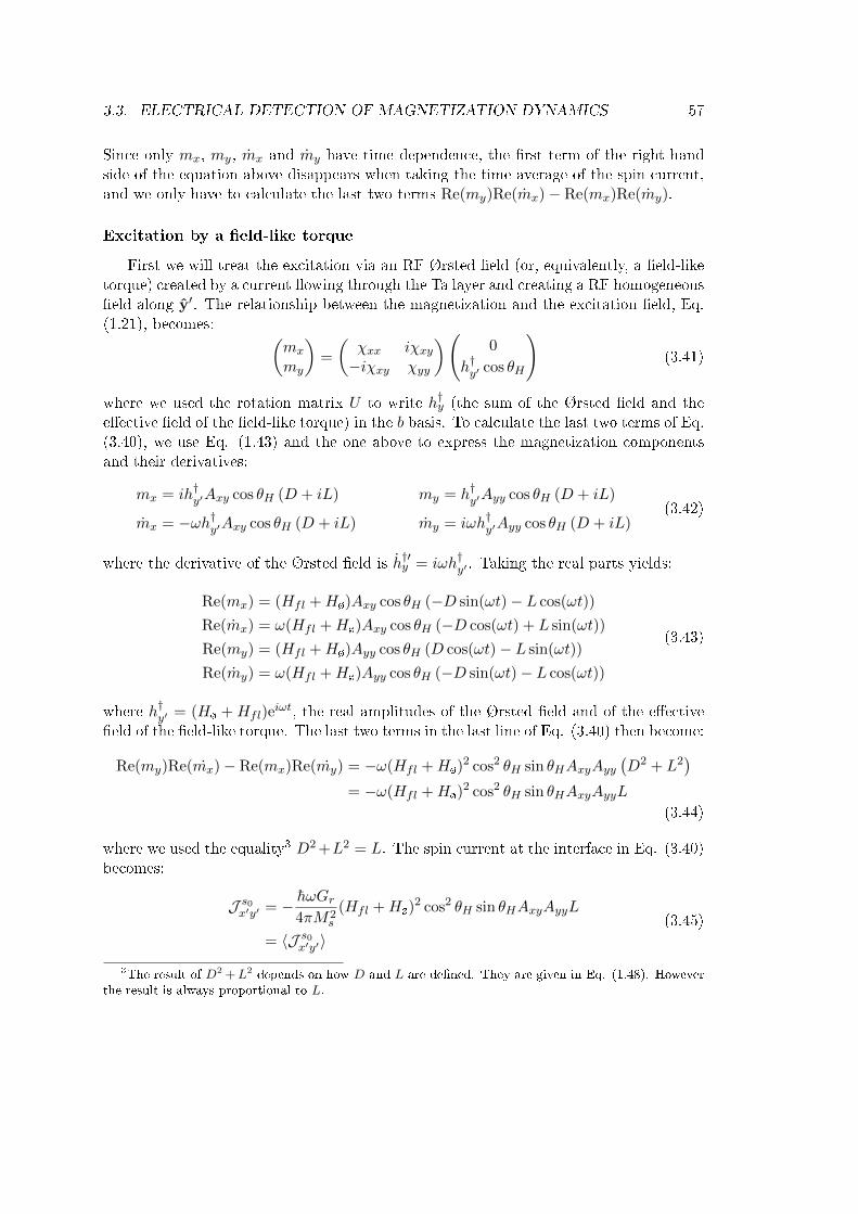
3.3. ELECTRICAL DETECTION OF MAGNETIZATION DYNAMICS 57
Since only mx, my, mx and my have time dependence, the rst term of the right handside of the equation above disappears when taking the time average of the spin current,and we only have to calculate the last two terms Re(my)Re(mx)− Re(mx)Re(my).
Excitation by a eld-like torque
First we will treat the excitation via an RF Ørsted eld (or, equivalently, a eld-liketorque) created by a current owing through the Ta layer and creating a RF homogeneouseld along y′. The relationship between the magnetization and the excitation eld, Eq.(1.21), becomes: (
mx
my
)=
(χxx iχxy−iχxy χyy
)(0
h†y′ cos θH
)(3.41)
where we used the rotation matrix U to write h†y (the sum of the Ørsted eld and theeective eld of the eld-like torque) in the b basis. To calculate the last two terms of Eq.(3.40), we use Eq. (1.43) and the one above to express the magnetization componentsand their derivatives:
mx = ih†y′Axy cos θH (D + iL)
mx = −ωh†y′Axy cos θH (D + iL)
my = h†y′Ayy cos θH (D + iL)
my = iωh†y′Ayy cos θH (D + iL)(3.42)
where the derivative of the Ørsted eld is h†′y = iωh†y′ . Taking the real parts yields:
Re(mx) = (Hfl +Hø)Axy cos θH (−D sin(ωt)− L cos(ωt))
Re(mx) = ω(Hfl +Hø)Axy cos θH (−D cos(ωt) + L sin(ωt))
Re(my) = (Hfl +Hø)Ayy cos θH (D cos(ωt)− L sin(ωt))
Re(my) = ω(Hfl +Hø)Ayy cos θH (−D sin(ωt)− L cos(ωt))
(3.43)
where h†y′ = (Hø + Hfl)eiωt, the real amplitudes of the Ørsted eld and of the eective
eld of the eld-like torque. The last two terms in the last line of Eq. (3.40) then become:
Re(my)Re(mx)− Re(mx)Re(my) = −ω(Hfl +Hø)2 cos2 θH sin θHAxyAyy
(D2 + L2
)= −ω(Hfl +Hø)
2 cos2 θH sin θHAxyAyyL
(3.44)
where we used the equality3 D2 +L2 = L. The spin current at the interface in Eq. (3.40)becomes:
J s0x′y′ = − hωGr4πM2
s
(Hfl +Hø)2 cos2 θH sin θHAxyAyyL
= 〈J s0x′y′〉(3.45)
3The result of D2 +L2 depends on how D and L are dened. They are given in Eq. (1.48). Howeverthe result is always proportional to L.

58 CHAPTER 3. SPIN-ORBIT TORQUES
The time dependence has disappeared, therefore the equation already gives the DC spincurrent at the interface. Combining Eq. (3.45) with Eq. (1.81), we have the expressionof the spin current as a function of depth as it decays in the NM:
〈J sx′y′〉 = 〈J s0x′y′〉sinh ((x− tn)/lsd)
sinh(tn/lsd)(3.46)
Then, by combining the equation above with Eq. (3.38) and integrating along the thick-ness and the width of the NM, we have an expression for the real charge current generatedby the iSHE in the NM that ows along the z′ axis:
〈Icz′〉 =2 e θSHh〈J s0x′y′〉
∫ ww2
−ww2
∫ tn
0
sinh ((x− tn)/lsd)
sinh(tn/lsd)dx′dy′
= −2wwlsd e θSHh
〈J s0x′y′〉 tanh
(tn
2lsd
) (3.47)
where tn is the thickness of the NM and lsd its spin diusion length, and ww is the widthof the SWW. Replacing J s0x′y′ by its expression in Eq. (3.45) we obtain:
〈Icz′〉 =ww eGrlsdθsh
2πM2s
ω(Hfl +Hø)2 cos2 θH sin θHAxyAyyL tanh
(tn
2lsd
)(3.48)
Finally, we can write the DC voltage that arises due to the combined eects of spin-pumping and the inverse spin Hall eect, under an Ørsted eld (or equivalently, a eld-like torque) excitation:
〈Vflishe〉 =ρnlw eGrlsdθsh
2πtnM2s
ω(Hfl +Hø)2 cos2 θH sin θHAxyAyyL tanh
(tn
2lsd
)(3.49)
where ρn is the resistivity of the NM and lw the length of the SWW. Thus, we ndthat the signal that is generated by the iSHE in the case of eld excitation has a purelyLorentzian lineshape.
Excitation by damping-like excitation
Now we shall calculate the voltage that arises from a damping-like torque excitation.Starting from Eq. (3.40), we must calculate the last two terms. The relationship betweenthe magnetization and the equivalent eld of the damping-like torque is given by:(
mx
my
)=
(χxx iχxy−iχxy χyy
)(hdl,x′ cos θH
0
)(3.50)
where we used the rotation matrix dened in Eq. (3.24). The components of the mag-netization and their derivatives are:
mx = hdl,x′Axx cos θH (D + iL)
mx = iωhdl,x′Axx cos θH (D + iL)
my = −ihdl,x′Axy cos θH (D + iL)
my = ωhdl,x′Axy cos θH (D + iL)(3.51)

3.3. ELECTRICAL DETECTION OF MAGNETIZATION DYNAMICS 59
Taking the real parts yields:
Re(mx) = HdlAxx cos θH (D cos(ωt)− L sin(ωt))
Re(mx) = ωHdlAxx cos θH (−D sin(ωt)− L cos(ωt))
Re(my) = HdlAxy cos θH (D sin(ωt) + L cos(ωt))
Re(my) = ωHdlAxy cos θH (D cos(ωt)− L sin(ωt))
(3.52)
where hdl,x′ = Hdl eiωt, Hdl being the real amplitude of the eective eld of the damping-
like torque along the x′ axis. The last two terms in the last line of Eq. (3.40) thenbecome:
Re(my)Re(mx)− Re(mx)Re(my) = −ωH2dl cos2 θH sin θHAxyAxxL (3.53)
which, apart from the eld amplitude and the term Axx replacing Ayy, is the same asEq. (3.44), where the excitation source is an Ørsted eld. Following the same steps asfor Eq. (3.49), we obtain:
〈Vdlishe〉 =ρnlw eGrlsdθsh
2πtnM2s
ωH2dl cos2 θH sin θHAxyAxxL tanh
(tn
2lsd
)(3.54)
Thus, we nd that the signal that is generated by the iSHE in the case of damping-liketorque excitation has a purely Lorentzian lineshape as well.
3.3.3 Conclusion: AMR vs iSHE
To conclude, we have calculated all the voltages that we expect to contribute to thesignals detected along the SWWs, under an in-plane saturating magnetic eld at an angleθH , and injecting an RF current in the SWW at a frequency ω. There are three possibleRF excitation sources in our Ta/FeCoB/MgO system: the damping-like torque, the eld-like torque and the Ørsted eld; the latter two being indiscernible. These excitationscan each combine with anisotropic magnetoresistance rectication or the combined spin-pumping and inverse spin Hall eect, resulting in a DC signal. This results in a linearcombination of up to 4 voltages, the lineshapes of which are summarized in Table 3.1.We recall the calculated voltages here for convenience:
〈Vflamr〉 =lw∆ρamrwwtfMs
cos2 θH sin θHIf (Hfl +Hø)AyyD
〈Vdlamr〉 =lw∆ρamrwwtfMs
sin(2θH) cos θHIfHdlAxyL
〈Vflishe〉 =lwρn eGrlsdθsh
2πtnM2s
tanh
(tn
2lsd
)cos2 θH sin θHω(Hfl +Hø)
2AxyAyyL
〈Vdlishe〉 =lwρn eGrlsdθsh
2πtnM2s
tanh
(tn
2lsd
)cos2 θH sin θHωH
2dlAxyAxxL
(3.55)

60 CHAPTER 3. SPIN-ORBIT TORQUES
where the terms Aij are dened in Eq. (1.48)4. The amplitudes If , (Hfl + Hø) andHdl are all proportional to the amplitude of the current applied to the whole SWW,therefore all 4 voltages scale with the RF power. Additionally, in this conguration allof the voltages have the same dependence on the in-plane angle θH of the applied eld,despite the dierent expressions of AMR and spin-pumping and the iSHE. However,AMR and the iSHE have a dierent out-of-plane angle dependence. The AMR andiSHE voltages have been calculated for numerous congurations by Harder et al. in[Har16], including dierent RF excitation directions, detection axes, and applied elddirections. Unfortunately we could not perform out-of-plane eld measurements withthe electromagnet at our disposal.
FeCoB alloys are known to have weak ρamr compared to NiFe alloys, and the propor-tion of current owing in the FeCoB layer is expected to be small given that the Ta layeris 4 times thicker than the FeCoB, at comparable resistivities. Another dierence liesin the frequency dependence of the signals, given by the direct dependence on ω as wellas via the Aij terms (see Eq. (1.48)). However such a study would require impedancematched devices so that signals at dierent frequencies can be easily compared. As canbe seen in Fig. 3.3 in Sec. 3.4, the variability of the amplitudes of the resonance peaksfor dierent frequencies indicates that the devices are not t for a frequency-dependentstudy.
This conclusion is supported when analyzing the lineshape. We give an example inFig. 3.4 in Sec. 3.4.1, which shows that the lineshape of the peak is Lorentzian, indicatingthat Vflamr, which is the only signal with a dispersive lineshape, is negligible. This impliesthat the studied system either does not exhibit eld-like torque or does not give a strongAMR signal. However, the eld-like torque has been measured in Ta/Fe72Co8B20/MgOsamples fabricated using the same deposition machine as our devices, by other measure-ment techniques [Gar13]. The eld-like torque has also been measured in similar Fe-richsystems such as Ta/Fe60Co20B20/MgO [Kim13]. Thus it is reasonable to expect similardependencies for the materials studied here, and the absence of a dispersive lineshape inour measurements indicates that the AMR signal is weak. With this, we conclude thatthe iSHE is the dominant source of the signal in our SWWs.
Moreover, the results of Chap. 4 are obtained in a conguration where the AMR con-tribution is expected to be minimum and the iSHE contribution maximum, indicatingthat the signals detected are purely the result of spin-pumping and the iSHE (see Sec.4.4.3). This is due to the dierent geometry of the excitation eld used for the experi-ments in Chap. 4 (as compared to Chap. 3), resulting in a dierent angle-dependencefor the AMR and the iSHE signals. In any case, the exact origin of the signal does notinuence the interpretation of the results shown in this chapter.
With the iSHE as the dominant source of the detected DC signal, it will not bepossible to distinguish between the contribution of the damping-like torque and of theeld-like torque excitation by comparing the relative amplitudes of the Lorentzian contri-
4In the case of a DC damping-like torque, the o-diagonal elements Axy are modied as seen in Eq.(3.20)

3.4. ST-FMR CHARACTERIZATION AT ZERO DC CURRENT 61
bution vs the dispersive contribution.5 Thus, the method used in [Ski14; Nan15; Pai15]cannot be used here to determine the relative strength of each spin-orbit torque.
RecticationExcitation Ørsted eld or
eld-like torqueDamping-like torque
AMR
iSHE
Table 3.1: Summary of the FMR lineshapes created by the possible excitation sourcesand the possible rectication methods.
3.4 ST-FMR characterization of Ta/FeCoB/MgO at zeroDC current
In this section, ST-FMR will be used to characterize materials properties of the SWW,using an RF current for the excitation of the ferromagnetic resonance, but without a DCcurrent.
By characterizing the resonance eld Hr and the resonance linewidth ∆H as a func-tion of frequency and FeCoB layer thickness, magnetic properties such as the saturationmagnetization, interfacial anisotropy and the damping can be obtained in principle. Allthe devices measured in this chapter have a width of ww = 1 µm. First we will describethe measurement protocol and verify the angle dependence that was calculated in Eq.(3.55). Thereafter we will present the dynamic ST-FMR characterization of the SWWat zero DC current.
3.4.1 Measurement protocol
A sinusoidal RF current, set at constant frequency throughout the measurement, issent through the SWW. The electromagnet is set such that the eld will be in the planeof the device at an angle θH = 68 with respect to the long axis of the SWW, as shownin Fig. 3.2. The magnetic eld is initially at µ0H = 0 mT and is then slowly decreasedto µ0H = −170 mT and then increased to µ0H = 170 mT, and nally decreased back
5In ST-FMR experiments performed on magnetic tunnel junctions, it is possible to dierentiate themdue to the fact that the damping-like torque is antisymmetric with respect to the current, whereas theeld-like torque is symmetric with respect to the current [Kub08].

62 CHAPTER 3. SPIN-ORBIT TORQUES
to µ0H = 0 mT. The eld step, for all segments, is 1 mT. The eld is swept across theresonance a total of 4 times: twice for negative elds and twice for positive elds. TheDC voltage is measured along the SWW, with the signal-to-noise ratio enhanced via themodulation of the RF power and the lock-in amplier.
Figure 3.3: ST-FMR resonances without DC current for an in-plane magnetized SWW,with a 1.33 nm thick FeCoB layer. The applied frequency ranges from 2.5 to 6.0 GHz.The uneven decrease of the resonance peak as the frequency increases is likely due toimpedance mismatch.
The result is a Lorentzian peak centered around the resonance eld Hr, with a non-zero linewidth ∆H, which in this work corresponds to the full width at half maximum(FWHM). Examples of eld sweep measurements are shown in Fig. 3.3 for dierentfrequencies of the RF current. The resonance peaks are then individually tted using aLorentzian function:
V = Vm
∆H2
4
(Hr −H)2 + ∆H2
4
+ V0 (3.56)
where H is the applied eld, V0 is an oset voltage, Hr is the resonance eld, Vm is themaximum voltage of the resonance peak and ∆H its full width at half maximum. Anexample of a Lorentzian function tted to a resonance peak is given in Fig 3.4. Thenon-zero oset voltage V0 will be discussed in Sec. 3.5 as it has a dependence on the DCcurrent used in the experiments described in that section.

3.4. ST-FMR CHARACTERIZATION AT ZERO DC CURRENT 63
Figure 3.4: ST-FMR resonance peak at 3.5 GHz without DC for an in-plane magnetizedSWW. A Lorentzian function, dened in Eq. (3.56), is tted to the curve, yieldingV0 = 2.45 µV, VA = 2.92 µV, Hr = 64.45 mT and ∆H = 5.4 mT.
Linearity with respect to RF power
The models and equations provided in Sec. 3.2 and 3.3 have been developed inthe linear approximation of the Landau-Lifshitz equation, which is inherently nonlinear.Thus, we must make sure that the magnetization dynamics we study are in the linearresponse regime. In the nonlinear regime, eects take place such as two magnon scatteringcan take place [Hei85; Hur98; Kri10]. The two-magnon scattering process involves thecoupling between the uniform FMRmode and degenerate spin-waves which have the sameresonance frequency, leading to increased relaxation of the uniform mode. In practice, thelinear regime is characterized by the FMR linewidth being proportional to the frequency,or the square of the resonance peak voltage being proportional to the absorbed RF power.
We attempted to reach the non-linearity by increasing the RF power up to the limitof our signal generator. When plotting the logarithm of the resonance peak voltage asa function of the power in dBm (resulting in a log-log plot), the peak voltage is stilllinear with respect to RF power even at +10 dBm. This is due to the fact that theSWW is not impedance-matched to the signal generator which has a source impedanceof 50Ω. Indeed, the 1 µm-wide SWWs have a resistance between 2 and 3 kΩ, resultingin a reection coecient of:
Γ =Zl − ZsZl + Zs
=2000− 50
2000 + 50≈ 95%
(3.57)
64 CHAPTER 3. SPIN-ORBIT TORQUES
where Zl is the SWW load impedance and where Zs is the source impedance of the signalgenerator, and we considered only purely resistive behavior. This means that less than5% of the RF power is transmitted to the SWW. For an RF power of +10 dBm at thethe signal generator output, only -3 dBm is transmitted to the SWW.6
In fact, the linearity limit can be observed in the data presented in Fig. 3.24 in Sec.3.5, where a DC current is added to the RF power in the SWW. The combined RF+DCpower in this case leads to non-linear behavior visible in the linewidth of the resonance.
3.4.2 Angle dependence
Since both AMR and the iSHE have the same angle dependence for an in-plane eldin ST-FMR, the two rectication eects cannot be decoupled this way. We neverthe-less performed an angle-dependent measurement to verify that the signal has at leastthe expected symmetry calculated in Eq. (3.55). The resonance peak amplitude as afunction of eld angle is shown in Fig. 3.5 and is tted by sin θH cos2 θH , which carriesthe expected symmetry for in-plane AMR and the iSHE, calculated in Sec. 3.3.1 and3.3.2. To completely ascertain the source of the signal, an out-of-plane angle-dependentmeasurement is necessary but such an electromagnet was not at out disposal.
The angular dependence in Fig. 3.5 shows that the signal has a maximum at 45 andminima at 0 and 90, which are repeated periodically. Therefore it would make sense toset the external eld at 45. This angle takes into account the angular dependence of thedetection mechanism (iSHE in our case) and the angular dependence of the excitationmechanism (a greater excitation would result in a larger precession cone and thus agreater signal). However, for the experiments in Sec. 3.5.1 and 3.5.2, where the DCeld-like and damping-like torques are studied, it is favorable to use an angle where theiramplitudes are maximized, which is 90. Thus, θH = 68 was chosen as a compromisebetween signal strength and DC torque eciency.
The contribution at resonance of the anomalous Nernst eect, which has a cos θHdependence on the applied eld angle [Sch12], can also be dismissed. This is due tothe extremely small thickness of the FM layer, which likely has a negligible temperaturegradient.
Another possible rectication is the spin Hall magnetoresistance,
3.4.3 Saturation magnetization and interfacial anisotropy
ST-FMR can be used to extract basic material parameters such as the saturationmagnetization and the interfacial anisotropy. By sweeping the eld while applying anRF current at constant frequency, we extract the resonance eld from the Lorentzian t,dened in Eq. (3.56). This measurement is repeated for a number of frequencies in theGHz range, at zero DC current for devices of dierent FM layer thickness, listed in Table
6In reality the transmission cables, contact probes, contact pads and the SWW itself all have compleximpedance. Since the SWW is much smaller than the wavelength in free space of the applied RF current,the impedances can be approximated by their real resistances. The other components have much smallerresistances than the SWW.
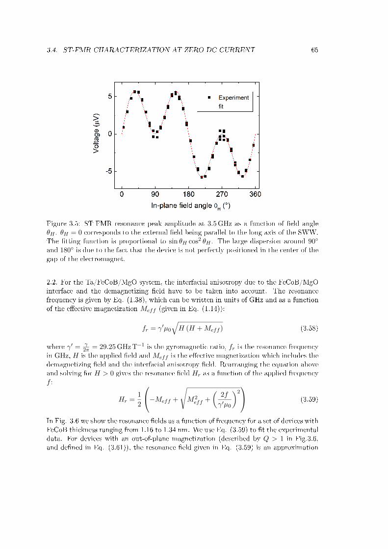
3.4. ST-FMR CHARACTERIZATION AT ZERO DC CURRENT 65
Figure 3.5: ST-FMR resonance peak amplitude at 3.5 GHz as a function of eld angleθH . θH = 0 corresponds to the external eld being parallel to the long axis of the SWW.The tting function is proportional to sin θH cos2 θH . The large dispersion around 90
and 180 is due to the fact that the device is not perfectly positioned in the center of thegap of the electromagnet.
2.2. For the Ta/FeCoB/MgO system, the interfacial anisotropy due to the FeCoB/MgOinterface and the demagnetizing eld have to be taken into account. The resonancefrequency is given by Eq. (1.38), which can be written in units of GHz and as a functionof the eective magnetization Meff (given in Eq. (1.14)):
fr = γ′µ0
√H (H +Meff ) (3.58)
where γ′ = γ2π = 29.25 GHz T−1 is the gyromagnetic ratio, fr is the resonance frequency
in GHz, H is the applied eld andMeff is the eective magnetization which includes thedemagnetizing eld and the interfacial anisotropy eld. Rearranging the equation aboveand solving for H > 0 gives the resonance eld Hr as a function of the applied frequencyf :
Hr =1
2
−Meff +
√M2eff +
(2f
γ′µ0
)2 (3.59)
In Fig. 3.6 we show the resonance elds as a function of frequency for a set of devices withFeCoB thickness ranging from 1.16 to 1.34 nm. We use Eq. (3.59) to t the experimentaldata. For devices with an out-of-plane magnetization (described by Q > 1 in Fig.3.6,and dened in Eq. (3.61)), the resonance eld given in Eq. (3.59) is an approximation

66 CHAPTER 3. SPIN-ORBIT TORQUES
under the assumption that the eld saturates the magnetization (this is further discussedat the end of this subsection). We extract Meff from the ts, and plot it as a functionof thickness in Fig. 3.7. The eective magnetization is related to the thickness by Eq.(1.14):
Meff = Ms −2Ki
µ0Mstf(3.60)
which allows us to linearly t the eective magnetization as a function of the inverseFeCoB thickness. The equation ts the data very well for devices with Meff > 0, butnot as much for devices with Meff < 0.
Figure 3.6: Resonance eld for devices with dierent ferromagnetic layer thickness. Eachdata set, identied by its color, corresponds to a device of a certain thickness and thecorresponding value indicated in the legend is the device's Q-factor, dened in Eq. (3.61).In-plane samples are characterized by Q < 1 and out-of-plane samples by Q > 1. Con-tinuous lines are tted to the data using Eq. (3.59).
The t yields Ms = (1.48± 0.04) MA m−1 for the saturation magnetization7 and aninterfacial anisotropy constant of Ki = (1.67± 0.07) mJ m−2, which results from bothinterfaces. The critical thickness where the magnetization switches from in-plane to out-of-plane magnetized, extracted from the condition Meff = 0, is tc = (1.21± 0.05) nm asshown in Fig. 3.7.
It is convenient to characterize the thickness dependence via the Q-factor8 which isthe ratio between the anisotropy eld and the demagnetizing eld, or equivalently the
7µ0Ms = (1.87 ± 0.05) T.8Not to be confused with the quality factor used to describe how underdamped a harmonic oscillator
is, or how sharp a resonance peak is relative to its base.

3.4. ST-FMR CHARACTERIZATION AT ZERO DC CURRENT 67
Figure 3.7: Eective magnetization as a function of the inverse of the ferro-magnetic layer's thickness. The linear t yields a saturation magnetization ofMs = (1.48± 0.04) MA m−1 and an interfacial anisotropy constant of Ki =(1.67± 0.07) mJ m−2. The top scale for tf is non-linear.
ratio between the anisotropy energy and the demagnetizing energy [Bea07]:
Q =2Ki
µ0M2s tf
=tctf
(3.61)
where the condition tf = tc is equivalent to Q = 1 and Meff = 0. Thus, in zero eld,an in-plane magnetized SWW is characterized by Q < 1 and an out-of-plane SWW byQ > 1. The devices measured in this chapter vary from Q = 0.90 (tf = 1.34 nm) toQ = 1.05 (tf = 1.16 nm). The relation between Q and tf is shown in Fig. 3.8. From nowon, data and devices will be referred to by their Q-factor, instead of their thickness.
We did not take into account a possible dead layer for the thickness of the ferromagnetand for the Q-factors described in this work. When a ferromagnetic layer is sputteredonto Ta (or vice-versa), part of the ferromagnetic material intermixes with the Ta. Theresulting non-magnetic layer is called the dead layer. It has been shown by Cuchet inher thesis [Cuc15], using the same deposition machine and the same FeCoB alloy, thatthe FeCoB/Ta interface results in a magnetic dead layer. The thickness of the dead layerdepends on the Ta thickness and on the order of deposition: for Ta deposited on topof FeCoB, it can be up to 0.6 nm thick, whereas for FeCoB deposited on top of Ta, itis only 0.3 nm. The thicker dead-layer resulting from the deposition of Ta on top of

68 CHAPTER 3. SPIN-ORBIT TORQUES
FeCoB can be explained by the bombardment of the latter by heavy Ta ions, increasingthe intermixing between the materials. In our case, since the Ta is deposited rst, weexpect a moderate dead layer thickness, but we have not measured it precisely. To givean idea of the Q-factor that would result from taking into a possible account dead layer,we provide in Fig. 3.8 the Q-factor for the devices (blue stars) calculated using:
Q =tc − tdtf − td
(3.62)
where the dead layer thickness estimate is td = 0.3 nm. The transition from out-of-planeto in-plane magnetization is dened by Q = 1 in both models. The values of Q forthe devices do not change signicantly because they are near Q = 1, which is wherethe dierence between the models with and without dead layers is smallest. If we as-sume 0.3 nm of dead layer, we obtain Ms = (1.15± 0.04) MA m−1 for the saturationmagnetization9 and Ki = (0.75± 0.07) mJ m−1 for the anisotropy constant.10 For com-parison, in [Cuc15], Cuchet found Ms = 1.03 MA m−1 with 0.24 nm of dead layer inTa(0.3)/Fe72Co8B20(1.2-2.2)/MgO (thicknesses in nm).11
While the possible errors for Ms and Ki are potentially signicant, most of the datarepresented in this chapter depend on either Q, which changes by up to 2.5% when ac-counting a dead layer of 0.3 nm, or onMeff , which is unaected. Due to the fact that wedid not measure the dead layer thickness, in this chapter we simply used the uncorrectedvalues of Q that do not take into account the dead layer thickness (black squares in Fig.3.8). The thicknesses we indicate for each device are the nominal thicknesses at eachposition on the wafer that we expect from the calibration of the deposition machine.Thus, any drift from the calibration introduces errors that we cannot easily account for.Therefore, in any thickness-dependent graph, the error bars do not take into account thepossible error in the thickness or the Q-factor of the device.
To demonstrate the self-consistency of the ts, we calculate the expected resonanceeld for fr = 3.5 GHz, which is the frequency used for the DC SOT characterization inSec. 3.5.1 and 3.5.2, using Eq. (3.59) as a function of the Q-factor, and compare it to theexperimental results. The results are shown in Fig. 3.9, and we nd that the calculatedvalues t the variation in thickness adequately.
In order to extract material parameters from FMR it is preferable to be in the con-dition where the equilibrium magnetization is aligned with the external eld's direction,i.e., the magnetization is saturated. The formulas for the FMR resonance eld and thelinewidth in Sec. 1.2.5 were derived under this condition. For SWWs with Q < 1 thisis always the case since the in-plane shape anisotropy is negligible. However for deviceswith Q > 1, we must verify that the magnetization is saturated by our electromagnet,which can apply a maximum eld of µ0H = 170 mT in the plane. Using the saturation
9µ0Ms = (1.44 ± 0.05) T.10This result is obtained by plotting µ0Meff as a function of (tf − 0.3 nm), where tf is the nominal
FeCoB thickness, and performing a linear t similarly to the one done in Fig. 3.7.11The composition is abbreviated. The full stack composition is:
substrate/Ta(3)/Pt(5)/(Co(0.5)/Pt(0.25))5/Co(0.5)/Ru(0.9)/(Co(0.5)/Pt(0.25))3/Co(0.5)/Ta(0.3)/Fe72Co8B20(1.2-2.2)/MgO/Fe72Co8B20(0.8-1.8)/Ta(1)/Pt(2) (thicknesses in nm).

3.4. ST-FMR CHARACTERIZATION AT ZERO DC CURRENT 69
Figure 3.8: Q-factor as a function of FeCoB thickness. Black squares are calculatedwithout consideration of a possible dead layer, using Eq. (3.61). Blue stars are calculatedby taking into account a dead layer 0.3 nm thick, using Eq. (3.62). However the abscissaused for the blue stars is the nominal FeCoB thickness tf .
magnetization and anisotropy constants obtained from the experiments, we calculate theresonance frequency for the saturated and unsaturated state as a function of the appliedeld for various Q-factors. The results are shown in Fig. 3.10. For a given Q-factor suchthat Q > 1, the resonance curve is described by two monotonic parts with the satura-tion eld Hsat marking a clear divide between the parts. For H < Hsat, the resonancefrequency fr decreases with the applied eld H while for H > Hsat, fr increases withH. Comparing Fig. 3.10 to Fig. 3.6, we see that the experimentally extracted resonanceelds for all thicknesses always increases with f , thus for all Q, the devices have beensaturated.12 With this, Eq. (3.59) gives a good approximation of the resonance eld fordevices with Q > 1. For SWWs with a Q-factor up to 1.08, the magnetization should besaturated by the maximum available eld. However, in practice we could not adequatelymeasure resonances for a SWW with a Q-factor higher than 1.05, therefore, devices withQ > 1.05 are not included in the discussions here.
3.4.4 Linewidth and damping in the absence of DC current
The eld linewidth ∆H can be used to extract information on the damping constantα of the material as well as inhomogeneous contributions to the linewidth. Using the
12Fig. 3.10 is a plot of resonance frequency as a function of applied eld, while Fig. 3.6 is a plot ofresonance eld as a function of applied frequency.

70 CHAPTER 3. SPIN-ORBIT TORQUES
Figure 3.9: Resonance eld as a function of Q-factor at 3.5 GHz. Eq. (3.59) and Eq.(3.61) are used to t the data as a function of Q.
expression of the Gilbert-type linewidth in Eq. (1.50) when H is near the resonance eldHr, the eld linewidth is related to the damping parameter:
∆H0 =2αfrγ′µ0
(3.63)
where γ′ is the gyromagnetic ratio in GHz T−1 and ∆H0 is the Gilbert-type contributionto the linewidth. However the linewidth can have other contributions, therefore insteadof calculating α from only one data point, the usual method is to measure the linewidthat several frequencies and to t the curve with a linear function. The slope is equal to
2αγ′µ0
according to Eq. (3.63). As an example, we show the linear tting of the linewidthin Fig. 3.11 for a device with Q = 0.91, obtaining α = 0.016. Unfortunately, not alldevices were investigated with the same range of frequencies,13 resulting in an incompletepicture in terms of linewidth vs. frequency, and thus α. Furthermore, while we were ableto measure the damping for devices with Q < 0.95, obtaining values in the 0.015− 0.020range, in other devices, especially those with Q > 1 and Q ≈ 1, the linewidth doesnot increase linearly with the frequency. Instead, it decreases or is non-linear, as shownin Fig. 3.12, and it is not possible to extract α for these SWWs in the small range offrequencies that we used, using Eq. (3.63). Additionally, we treated the devices as thin
13This is due to several factors. For high frequencies, the resonance eld exceeds the maximum eldthe electromagnet can generate. For lower frequencies, the resonance eld approaches zero, where themeasurement setup produces an unexplained large noisy peak, which can overlap with the resonancepeak. Additionally, the bias-T imposed its own limit on low frequencies for f < 1 GHz.
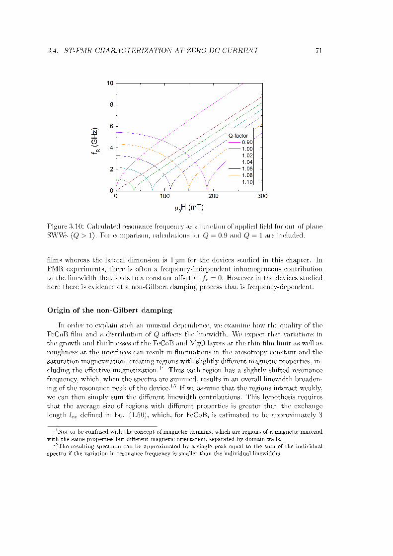
3.4. ST-FMR CHARACTERIZATION AT ZERO DC CURRENT 71
Figure 3.10: Calculated resonance frequency as a function of applied eld for out-of-planeSWWs (Q > 1). For comparison, calculations for Q = 0.9 and Q = 1 are included.
lms whereas the lateral dimension is 1µm for the devices studied in this chapter. InFMR experiments, there is often a frequency-independent inhomogeneous contributionto the linewidth that leads to a constant oset at fr = 0. However in the devices studiedhere there is evidence of a non-Gilbert damping process that is frequency-dependent.
Origin of the non-Gilbert damping
In order to explain such an unusual dependence, we examine how the quality of theFeCoB lm and a distribution of Q aects the linewidth. We expect that variations inthe growth and thicknesses of the FeCoB and MgO layers at the thin lm limit as well asroughness at the interfaces can result in uctuations in the anisotropy constant and thesaturation magnetization, creating regions with slightly dierent magnetic properties, in-cluding the eective magnetization.14 Thus each region has a slightly shifted resonancefrequency, which, when the spectra are summed, results in an overall linewidth broaden-ing of the resonance peak of the device.15 If we assume that the regions interact weakly,we can then simply sum the dierent linewidth contributions. This hypothesis requiresthat the average size of regions with dierent properties is greater than the exchangelength lex dened in Eq. (1.60), which, for FeCoB, is estimated to be approximately 3
14Not to be confused with the concept of magnetic domains, which are regions of a magnetic materialwith the same properties but dierent magnetic orientation, separated by domain walls.
15The resulting spectrum can be approximated by a single peak equal to the sum of the individualspectra if the variation in resonance frequency is smaller than the individual linewidths.

72 CHAPTER 3. SPIN-ORBIT TORQUES
Figure 3.11: Linewidth as a function of inverse thickness for a SWW with Q = 0.91. Thet yields a damping parameter α = 0.016.
nm depending on the value of Ms.16 We were not able to quantify that the average sizeof such regions is greater than lex, though with the Brillouin light scattering microscopedescribed in Sec. 4.5, which has a spatial resolution of 250 nm, we were able to observevariations in the local eective magnetization. Thus we assume that the sizes of theregions described above are large enough. We write the total linewidth:
∆H = ∆H0 + ∆Hin (3.64)
where ∆H0 is the Gilbert-type linewidth given in Eq. (3.63) and ∆Hin represents thefrequency-dependent non-linear linewidth contribution due to the inhomogeneity of themagnetic properties of the SWW.
The linewidth broadening arises from the uctuations of the resonance eld over thevolume. As written in Eq. (3.59), the resonance eld is a function of the FeCoB thickness,the anisotropy constant and the saturation magnetization. Thus, for a xed frequency,we can estimate a nite variation of the resonance eld using its partial derivatives,following McMichael's example [McM04]:
∆Hr = 2
√(∂Hr
∂Ms
)2
∆M2s +
(∂Hr
∂Ki
)2
∆K2i +
(∂Hr
∂tf
)2
∆t2f
∆Hr = ∆Hin
(3.65)
where ∆t, ∆Ki and ∆Ms represent the dispersion of the values of the FeCoB thickness,the anisotropy constant and the saturation magnetization, assuming that the magnetic
16Assuming Aex = 10 pJ m−1 from [Bel17] and Ms = 1.48 MA m−1, we obtained lex = 2.7µm.

3.4. ST-FMR CHARACTERIZATION AT ZERO DC CURRENT 73
Figure 3.12: Linewidth as a function of inverse thickness for a SWW with Q = 1.02.
properties of the dierent regions have Gaussian distributions. The Q-factor is a functionof the same variables, therefore the dispersion of the values of Q (dened in Eq. (3.61))can be written as:
∆Q = 2
√(∂Q
∂Ms
)2
∆M2s +
(∂Q
∂Ki
)2
∆K2i +
(∂Q
∂tf
2)∆t2f (3.66)
We can use this result to write ∆Hin as a function of ∆Q only:
∆Hin = 2
√(∂Hr
∂Q
∂Q
∂Ms
)2
∆M2s +
(∂Hr
∂Q
∂Q
∂Ki
)2
∆K2i +
(∂Hr
∂Q
∂Q
∂tf
)2
∆t2f
= 2
∣∣∣∣∂Hr
∂Q
∣∣∣∣√(
∂Q
∂Ms
)2
∆M2s +
(∂Q
∂Ki
)2
∆K2i +
(∂Q
∂t
)2
∆t2f
=
∣∣∣∣∂Hr
∂Q
∣∣∣∣∆Q(3.67)
Thus, we can study the eect of the variations of all these quantities on the linewidthusing a single uctuating parameter ∆Q. Before calculating the derivative in the equationabove, we rewrite the resonance eld in Eq. (3.59) as a function of the Q-factor:
Hr =1
2
−Ms(1−Q) +
√M2s (1−Q)2 +
(2ω
γ
)2 (3.68)
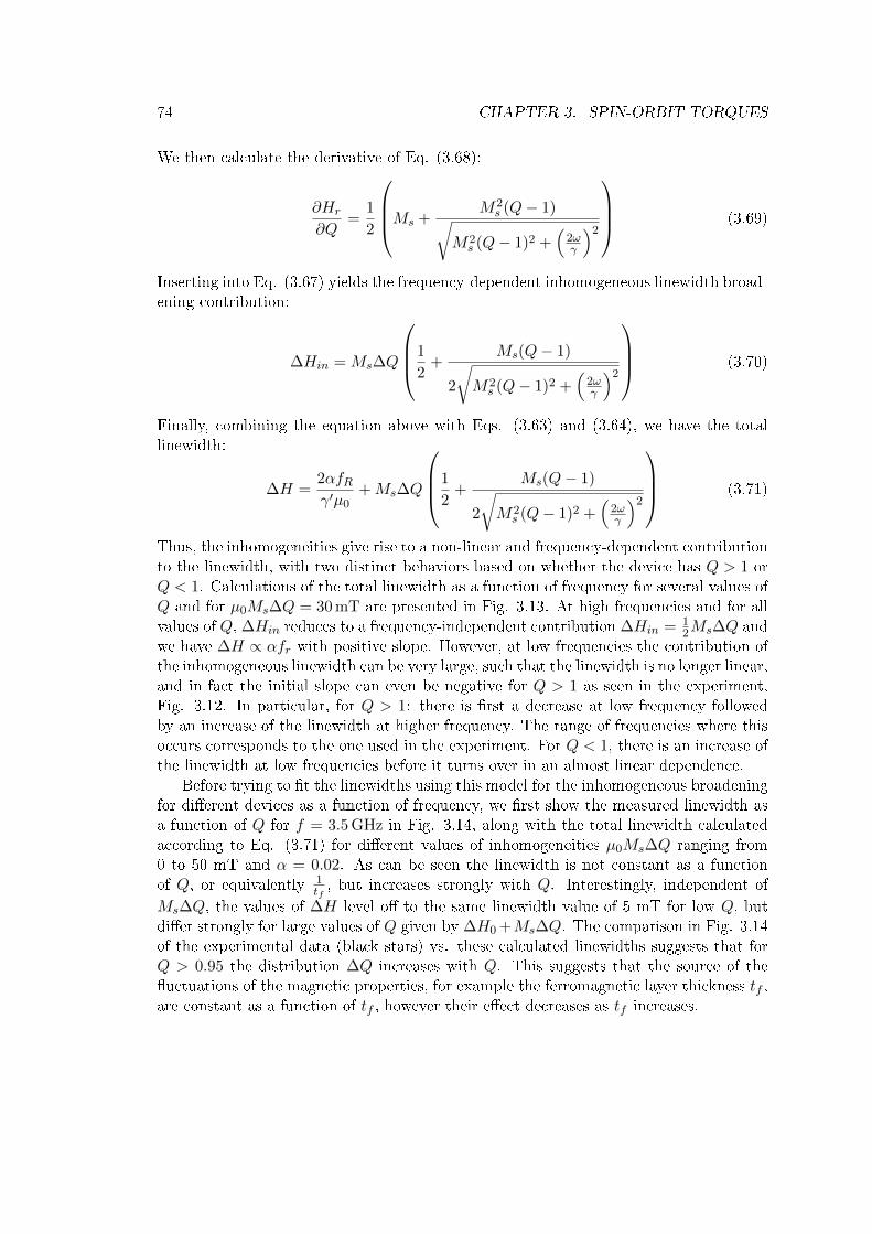
74 CHAPTER 3. SPIN-ORBIT TORQUES
We then calculate the derivative of Eq. (3.68):
∂Hr
∂Q=
1
2
Ms +M2s (Q− 1)√
M2s (Q− 1)2 +
(2ωγ
)2
(3.69)
Inserting into Eq. (3.67) yields the frequency-dependent inhomogeneous linewidth broad-ening contribution:
∆Hin = Ms∆Q
1
2+
Ms(Q− 1)
2
√M2s (Q− 1)2 +
(2ωγ
)2
(3.70)
Finally, combining the equation above with Eqs. (3.63) and (3.64), we have the totallinewidth:
∆H =2αfRγ′µ0
+Ms∆Q
1
2+
Ms(Q− 1)
2
√M2s (Q− 1)2 +
(2ωγ
)2
(3.71)
Thus, the inhomogeneities give rise to a non-linear and frequency-dependent contributionto the linewidth, with two distinct behaviors based on whether the device has Q > 1 orQ < 1. Calculations of the total linewidth as a function of frequency for several values ofQ and for µ0Ms∆Q = 30 mT are presented in Fig. 3.13. At high frequencies and for allvalues of Q, ∆Hin reduces to a frequency-independent contribution ∆Hin = 1
2Ms∆Q andwe have ∆H ∝ αfr with positive slope. However, at low frequencies the contribution ofthe inhomogeneous linewidth can be very large, such that the linewidth is no longer linear,and in fact the initial slope can even be negative for Q > 1 as seen in the experiment,Fig. 3.12. In particular, for Q > 1: there is rst a decrease at low frequency followedby an increase of the linewidth at higher frequency. The range of frequencies where thisoccurs corresponds to the one used in the experiment. For Q < 1, there is an increase ofthe linewidth at low frequencies before it turns over in an almost linear dependence.
Before trying to t the linewidths using this model for the inhomogeneous broadeningfor dierent devices as a function of frequency, we rst show the measured linewidth asa function of Q for f = 3.5 GHz in Fig. 3.14, along with the total linewidth calculatedaccording to Eq. (3.71) for dierent values of inhomogeneities µ0Ms∆Q ranging from0 to 50 mT and α = 0.02. As can be seen the linewidth is not constant as a functionof Q, or equivalently 1
tf, but increases strongly with Q. Interestingly, independent of
Ms∆Q, the values of ∆H level o to the same linewidth value of 5 mT for low Q, butdier strongly for large values of Q given by ∆H0 +Ms∆Q. The comparison in Fig. 3.14of the experimental data (black stars) vs. these calculated linewidths suggests that forQ > 0.95 the distribution ∆Q increases with Q. This suggests that the source of theuctuations of the magnetic properties, for example the ferromagnetic layer thickness tf ,are constant as a function of tf , however their eect decreases as tf increases.

3.4. ST-FMR CHARACTERIZATION AT ZERO DC CURRENT 75
Figure 3.13: Calculated total linewidth µ0∆H as a function of frequency for values ofQ ranging from 0.86 to 1.04. The linewidth is calculated using (3.71) with α = 0.02and µ0Ms∆Q = 30 mT for all curves. The inhomogeneous linewidth contribution isresponsible for the non-linear behavior at low frequency (approximately < 3 GHz) of thetotal linewidth for Q 6= 0, as well as the initial value at f = 0 for Q ≥ 0.
Due to this dependence, we tted the total linewidth ∆H vs. the frequencyf for eachSWW of dierent thickness, where Ms∆Q was the tting parameter. In principle thereis also a thickness-dependent contribution to the damping arising from spin-pumping αsp[Tse02a; Tse05], but it would be dicult to t the experimental data keeping bothMs∆Qand α + αsp as t parameters for devices of dierent Q. Therefore, for the qualitativestudy we present here, we assumed α to be constant using a value of 0.02 based on therelatively constant linewidth at f = 3.5 GHz found for 3 devices with 0.91 < Q < 0.93(see ts shown in Fig. 3.14).17 These devices also present the smallest linewidths. Thisis under the assumption that for these values of Q, the inhomogeneous contribution issmall compared to the Gilbert-type damping and spin-pumping.
We present in Fig. 3.15 the linewidths plotted as a function of frequency for SWWswith dierent Q-factors. Eq. (3.71) is tted to each curve, usingMs∆Q as tting variable.The accuracy of the tted total linewidth varies greatly from device to device and therange of frequencies used for some SWWs is insucient for a satisfying t. Thus we are far
17For these 3 devices, we assume the damping to be constant because the contribution of spin-pumpingto the eective damping is small due to the small variation in thickness between the devices. Weextracted the real part of the spin mixing conductance Gr by plotting αeff vs. 1/tf and using αeff =α+hγGr/(4πMstf ) (see Eq. (60) in [Tse05]) from 4 separately prepared samples with FeCoB thicknessesof 2.5, 5, 20 and 40 nm, obtaining Gr ≈ 12 nm−2. This results in variations of 2% due to spin-pumpingfor the eective damping for the very small thickness range covered by the three devices.

76 CHAPTER 3. SPIN-ORBIT TORQUES
Figure 3.14: Linewidth as a function of Q for fr = 3.5 GHz. Lines represent calculatedlinewidths for values of µ0Ms∆Q ranging from 0 to 50 mT, with α = 0.02. Stars representexperimental data.
from a quantitative agreement. However the inhomogeneous linewidth broadening modelis capable of qualitatively predicting the non-linear behavior: for Q < 1, it accounts forthe increase of the linewidth with respect to intrinsic linewidth, and for Q > 1, it explainsthe initial decrease of the linewidth at low frequencies. We summarize the t results inFig 3.16. The inhomogeneity distribution ∆Q linearly increases as Q increases, indicatingthat the thinner the FeCoB layer, the greater the eect of the inhomogeneities on thelinewidth, conrming the interfacial nature of its origin.
In this section we neglected an important contribution to the linewidth, which isspin-pumping (see Sec. 1.4.3). Spin-pumping is a relaxation channel that increasesthe eective damping, and its role increases as the FeCoB thickness decreases, due tobeing an interfacial eect. While we neglected spin-pumping in this subsection, it cannotaccount for the decrease of linewidth for devices with Q > 1 at low frequencies sincethe contribution of spin-pumping to the eective damping is positive. Thus, a thickness-dependent eective damping parameter does not call into question our model. However,a quantitative validation of our model would require accurately measuring the eectivedamping at high frequencies such that ∆H ∝ αefffr, as well as taking into accountspin-pumping, whose contribution can be obtained by performing a thickness-dependentstudy.

3.4. ST-FMR CHARACTERIZATION AT ZERO DC CURRENT 77
Figure 3.15: Linewidths as a function of frequency for devices with Q ranging from 1.044to 0.905. Symbols represent experimental data. Each data set is tted by Eq. (3.71),with α = 0.02, and represented by either full or dashed lines. Some curves cross due tothe fact that dierent values of Ms∆Q were used for each device.
Figure 3.16: Summary of the tted parameter µ0Ms∆Q (squares) as a function of Q,obtained from tting Eq. (3.71) to the experimental data. The linear t (red line) doesnot take into account the red square data point.

78 CHAPTER 3. SPIN-ORBIT TORQUES
3.5 ST-FMR characterization of Ta/FeCoB/MgO with DCcurrent
We now seek to characterize how the spin-orbit torques generated by a DC currentwithin the Ta layer as well as at the Ta/ FeCoB interface aect the magnetization dynam-ics. In Sec. 3.3 it was shown that the RF excitation, whether by the Ørsted eld or bythe SOTs, results in Lorentzian resonance peaks in the case where the rectication phe-nomenon is the iSHE. Thus, it is impossible to characterize the SOTs with RF currentsin these devices. However, if in addition a DC current is injected, each torque changesthe susceptibility components, as shown in Sec. 3.2.3 and 3.2.4: the eld-like torqueis expected to shift the resonance eld, and the damping-like torque is expected to en-hance or reduce the resonance linewidth. This technique was used for bilayers in [Liu11;Kas14; Nan15] as well as for the characterization of spin Hall nanoscillators [Zah18] andmagnetic tunnel junctions [Tar18].
Figure 3.17: Example of ST-FMR resonances for a device with Q = 0.974. The symbolsrepresent experimental data, the red curves are Lorentzian functions tted to the data,and the vertical dashed lines are guides for the eye to indicate resonance elds. Withnear zero DC current injected (black symbols), the resonances are antisymmetric withrespect to the eld. With -0.8 mA DC (green symbols), the resonance at negative eldhas reduced linewidth while the resonance at positive eld has increased linewidth. With+0.8 mA DC (blue symbols), this behavior is reversed with respect to the eld. For both-0.8 and +0.8 mA DC, the resonance eld is shifted toward zero.
In Fig. 3.17, we give an example of resonance peaks measured for the same device,at 3.5 Ghz, for 3 dierent currents. The black symbols represent data taken at Idc =−0.01 mA, which for this paragraph serves as the zero DC current example. For thiscurrent, the resonance eld and the linewidth of the peaks at negative eld and positiveeld are equal in magnitude. The blue symbols represent data taken at Idc = 0.8 mA.

3.5. ST-FMR CHARACTERIZATION WITH DC CURRENT 79
For both eld polarities the resonance peak is shifted toward smaller absolute eld values,however the shift is more pronounced for H > 0. Additionally, the peak at H > 0 has asmaller linewidth than the peak at H < 0. For data taken at Idc = −0.8 mA, symbolizedby green circles, there is also a shift of the resonance eld toward smaller values for bothpolarities, but this time the shift is greater for H < 0. Likewise, the linewidth is smallerat H < 0 than for H > 0 for the data represented by the green circles. It is this eld andcurrent dependent behavior that we will study to characterize the eld-like torque andthe damping-like torque in the next two subsections, for devices of dierent Q-factor.
The measurement protocol is similar as in the previous section: the eld is swept at a68 angle, starting at 0 and down to µ0H = −170 mT, then back to 0. The measurementis then immediately repeated for positive elds. In addition, measurements are made atdierent DC currents, from -1 to +1 mA, in steps of 0.1 or 0.2 mA. Thus, each pair ofeld polarity and current polarity is measured twice. Due to the limited magnetic eldrange available, we could not vary the frequency to a reasonable range on all devices(due to the resonance moving outside the eld range. Thus we limit the frequency usedin this section to 3.5 GHz. We remind that all of the devices measured in this chapterhave a width of ww = 1 µm.
Oset voltage dependence on Idc
As mentioned in Sec. 3.4.1, the detected signal has an oset voltage, shown by V0
in Fig. 3.4, which is dependent of the DC current (in Fig. 3.17, the oset voltages havebeen removed to compare the resonance peaks).
Though a contribution of the anomalous Nernst eect (ANE) to the peak resonancesignal was dismissed in Sec. 3.4.2, it be responsible for the oset voltage. It has beenmeasured in a system similar to ours, Ta/Fe60Co20B20/MgO [Tu17]. The ANE is ob-served when a ferromagnet is has a thermal gradient, resulting in an electric eld that isperpendicular to both the thermal gradient and the FM's magnetization. In the SWWs,it is likely that there is a heat gradient perpendicular to the layers, due to uniform Jouleheating by the RF current and asymmetric heat dissipation between the top and bottominterfaces of the SWW. The RF power is modulated by the lock-in amplier, thereforethe heat gradient also varies at the modulation frequency. Thus, a Nernst voltage can bedetected by the lock-in amplier. In the experiments described in this section, an addi-tional DC current is injected in the SWW, and the oset voltage increases considerablywith the current. Fig. 3.18 shows the oset voltage vs. the applied DC current Idc forseveral frequencies. The following function ts the experimental data adequately:
V0 = a+ b sgn(Idc) Idc + c I2dc (3.72)
where sgn(Idc) gives the sign of Idc, and a, b > 0 and c < 0. The Nernst eect contributesto a. We expect the dynamic resistance of the SWW (due to Joule heating via themodulated RF current) to contribute to b. However we did not identify a possible causefor c which is negative nor for the dependence on sgn(Idc) of the linear term.
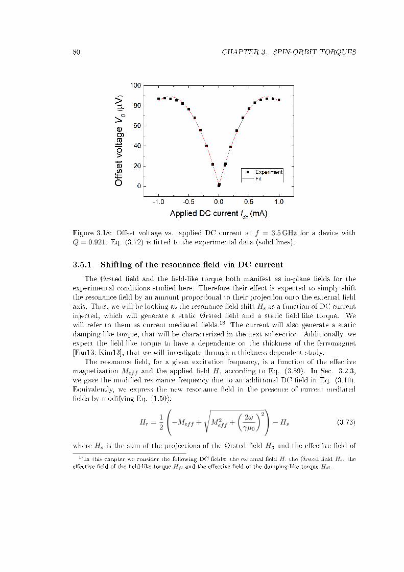
80 CHAPTER 3. SPIN-ORBIT TORQUES
Figure 3.18: Oset voltage vs. applied DC current at f = 3.5 GHz for a device withQ = 0.921. Eq. (3.72) is tted to the experimental data (solid lines).
3.5.1 Shifting of the resonance eld via DC current
The Ørsted eld and the eld-like torque both manifest as in-plane elds for theexperimental conditions studied here. Therefore their eect is expected to simply shiftthe resonance eld by an amount proportional to their projection onto the external eldaxis. Thus, we will be looking at the resonance eld shift Hs as a function of DC currentinjected, which will generate a static Ørsted eld and a static eld-like torque. Wewill refer to them as current-mediated elds.18 The current will also generate a staticdamping-like torque, that will be characterized in the next subsection. Additionally, weexpect the eld-like torque to have a dependence on the thickness of the ferromagnet[Fan13; Kim13], that we will investigate through a thickness-dependent study.
The resonance eld, for a given excitation frequency, is a function of the eectivemagnetization Meff and the applied eld H, according to Eq. (3.59). In Sec. 3.2.3,we gave the modied resonance frequency due to an additional DC eld in Eq. (3.10).Equivalently, we express the new resonance eld in the presence of current-mediatedelds by modifying Eq. (1.50):
Hr =1
2
−Meff +
√M2eff +
(2ω
γµ0
)2−Hs (3.73)
where Hs is the sum of the projections of the Ørsted eld Hø and the eective eld of18In this chapter we consider the following DC elds: the external eld H, the Ørsted eld Hø, the
eective eld of the eld-like torque Hfl and the eective eld of the damping-like torque Hdl.
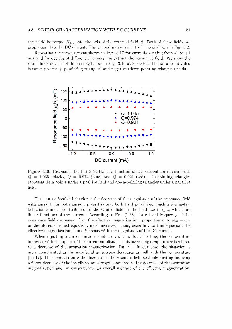
3.5. ST-FMR CHARACTERIZATION WITH DC CURRENT 81
the eld-like torque Hfl, onto the axis of the external eld, z. Both of these elds areproportional to the DC current. The general measurement scheme is shown in Fig. 3.2.
Repeating the measurement shown in Fig. 3.17 for currents ranging from -1 to +1mA and for devices of dierent thickness, we extract the resonance eld. We show theresult for 3 devices of dierent Q-factor in Fig. 3.19 at 3.5 GHz. The data are dividedbetween positive (up-pointing triangles) and negative (down-pointing triangles) elds.
Figure 3.19: Resonance eld at 3.5 GHz as a function of DC current for devices withQ = 1.035 (black), Q = 0.974 (blue) and Q = 0.921 (red). Up-pointing trianglesrepresent data points under a positive eld and down-pointing triangles under a negativeeld.
The rst noticeable behavior is the decrease of the magnitude of the resonance eldwith current, for both current polarities and both eld polarities. Such a symmetricbehavior cannot be attributed to the Ørsted eld or the eld-like torque, which arelinear functions of the current. According to Eq. (1.38), for a xed frequency, if theresonance eld decreases, then the eective magnetization, proportional to ωM − ωKin the aforementioned equation, must increase. Thus, according to this equation, theeective magnetization should increase with the magnitude of the DC current.
When injecting a current into a conductor, due to Joule heating, the temperatureincreases with the square of the current amplitude. This increasing temperature is relatedto a decrease of the saturation magnetization [Du 19]. In our case, the situation ismore complicated as the interfacial anisotropy decreases as well with the temperature[Lee17]. Thus, we attribute the decrease of the resonant eld to Joule heating inducinga faster decrease of the interfacial anisotropy compared to the decrease of the saturationmagnetization and, in consequence, an overall increase of the eective magnetization.
82 CHAPTER 3. SPIN-ORBIT TORQUES
This phenomenon is well known and is exploited to more easily control the magnetizationof a storage layer in MRAM via heating in a thermally assisted switching scheme [Pre13;Str18].
Since the saturation magnetization and the interfacial anisotropy vary with temper-ature, which itself varies with the square of the current, they are both even functions ofthe current. There are other temperature eects that may give rise to a voltage in ourexperiment, such as the Nernst eect [Tu17], but none are expected to shift the resonanceeld. A simple method of eliminating the even component of a function and keeping onlythe odd component is to calculate:
Hr,odd(I) =Hr(I)−Hr(−I)
2(3.74)
Thus, we eliminate all temperature-dependent eects from the resonance eld. Theonly odd functions of the current, that we know of, that can change the resonance eldare the Ørsted eld and the eld-like torque, which are linear with current.19 Garelloet al. [Gar13] have shown evidence of higher order SOTs, relative to the angle of themagnetization, though they are still odd functions of the current. We did not considerthem here because their eects on the magnetization dynamics are weaker than the twoSOT terms we consider in this work.20
In Fig. 3.20, we show the odd part of the resonance eld, extracted using Eq. (3.74),for a device with Q < 1 and for a device with Q > 1.21 The graph shows a lineartrend for both samples, though the slope is positive and small for Q = 0.913, while itis negative and large for Q = 1.035. We linearly t the data only for H > 0 since theother half of the graph contains the same information. The slope of the linear t, whichis the resonance eld shift per unit current, is attributed to the eld-like torque and theØrsted eld. Thus, we have:
∂Hr,odd
∂Idc=∂Hs
∂Idc(3.75)
This treatment of the extracted resonance eld is repeated for devices of dierent Q-factor. In Fig. 3.21, we plot ∂Hs
∂Idcas a function of Q, extracted from linear ts and
averaged for results from positive and negative elds. The graph shows that ∂Hs∂Idcincreases
in magnitude with Q, with a change of sign around Q = 0.93. Such a change of sign isindicative of two opposing eects: the eld-like torque and the Ørsted eld.
19Large values of the damping-like and eld-like torque can also change the resonance eld by changingthe equilibrium position of the magnetization, and thus the expression of the resonance eld, however weneglect this in our calculations. Indeed, the external eld, when reaching the value of resonance, is twoorders of magnitude larger than the eective elds of the eld-like and damping-like torques we measurein this chapter.
20This conclusion was reached after performing simulations on a uniform magnetization, adding theSOT terms one by one, using the values for Ta/FeCoB in [Gar13].
21For some devices, there is an unidentied oset that is dependent on the sign of the current, resultingin two parallel curves that do not meet at the origin. We were not able to explain this discrepancy. Sincewe are interested in the slope of the linear t, an oset does not change the treatment of the data.

3.5. ST-FMR CHARACTERIZATION WITH DC CURRENT 83
Figure 3.20: Odd component of the resonance eld with respect to the applied cur-rent, calculated according to Eq. (3.74). Only the Ørsted eld and the eld-like torquecontributions, which are odd functions of the DC current, are kept. Blue triangles rep-resent resonance elds for positive (up-pointing) and negative (down-pointing) elds forQ = 0.913. Black triangle represent resonance elds for positive (up-pointing) and neg-ative (down-pointing) elds for Q = 1.035. For Idc > 0, full lines are linear ts of thepositive eld data points, while dashed lines are linear ts of the negative eld datapoints.
We estimate the Ørsted eld under the following considerations: only part of theDC current goes into the Ta layer and the magnetic eld is applied at a 68 angle withrespect to the SWW long axis.
Let us make an estimation of the Ørsted eld by only considering the one generatedby the DC current in the Ta layer, It. We will not calculate the Ørsted eld generatedby the current in the FeCoB layer, as its net eect on itself is negligible compared to theeld generated by the Ta layer. Using Ørsted's law, we calculate the eld in the FeCoBlayer, far from the lateral and longitudinal edges, where it is assumed to be the strongestand parallel to the interface. The Ørsted eld is approximated for very thin wires, i.e.,their thickness is much smaller than their width, by:
Hø =It2d
(3.76)
where d is the width of the wire and It is the current that ows in the Ta layer. Atthis stage, we do not know whether Hø and Hfl have the same sign or not,22 thus we
22The absolute direction of the Ørsted eld could have been determined from the direction of thecurrent, however this information was lost to entropy.

84 CHAPTER 3. SPIN-ORBIT TORQUES
Figure 3.21: Shift of the resonance eld per unit of current as a function of Q. Each datapoint is the average of the slopes of the linear t of the odd part of the resonance eld,for positive and negative elds, as a function of applied current.
can write the contribution of the Ørsted eld as δø∂Hø
∂It, where δø = +1 if the elds are
parallel, and δø = −1 if not.Additionally, the external eld is at a 68 angle with respect to the SWW. The change
in resonance eld is due to the projection of the current-mediated elds onto the axis ofthe external eld. Therefore the elds are overestimated by a factor of cos 22. Thus, wehave:
µ0∂Hs
∂Idc= µ0
(∂Hfl
∂Idc+ δø
∂Hø
∂Idc
)cos 22 (3.77)
Next, the SWW contains two conductive layers, Ta and FeCoB. Let us make a roughestimation of the fraction of the current that goes through the Ta layer, under theassumption that the two layers can be assimilated to two parallel resistances:
ItIdc
=
ρftf
ρftf
+ ρntn
(3.78)
where It is the current that goes through the Ta layer, ρf and tf are the resistivity andthe thickness of the FeCoB layer, and ρn and tn are the resistivity and the thickness ofthe Ta layer. The resistivity of Ta was measured to be ρn = 196 µΩ cm for a 5 nm thickTa lm23 and the resistivity of FeCoB was measured to be ρf = 275 µΩ cm for a 1.5 nm
23The Ta test sample was not capped, thus we may expect a lower resistivity for the 5 nm Ta in theSWW.

3.5. ST-FMR CHARACTERIZATION WITH DC CURRENT 85
thick lm capped by 2 nm of naturally oxidized aluminum.24 Finally the ratio of currentthat goes through the Ta layer is 85%, when using an average thickness of FeCoB, 1.2nm, according to Eq. (3.78). This ratio varies by ±1% for the two extreme thicknessesinvolved, thus we use this average value for all devices.
For each slope that we extract from the odd part of the resonance eld shift we makethe following correction :
µ0∂Hfl
∂It= µ0
(1
cos 22IdcIt
∂Hs
∂Idc− δø
∂Hø
∂It
)= µ0
(1
cos 22IdcIt
∂Hs
∂Idc− δø
1
2d
) (3.79)
where ∂Idc∂It
= IdcIt.
Finally, we report the strength of the eld-like torque βfl as a function of Q inunits of T m2 A−1 in Fig. 3.22 by multiplying by the cross section of the Ta layer,ww × tn = 1 µm× 5 nm:
βfl = wwtnµ0∂Hfl
∂It(3.80)
In Fig. 3.22, we show βfl in the case where Hfl is parallel to the Hø (black squares) andin the case where they are anti-parallel (blue circles). Under the assumption that theØrsted eld varies little with Q (see Eq. (3.76)), and that βfl can vary with Q, we inferthat the change of sign of ∂Hs∂Idc
in Fig. 3.21 signies that Hfl and Hø have the same signfor Q < 0.94 and opposite sign for Q > 0.94. Thus, we conclude that the blue circles inFig. 3.22 represent βfl correctly.
In Fig. 3.22, we drew a line suggesting that βfl follows a linear trend with Q, i.e., βflis inversely proportional to the ferromagnetic layer thickness tf . This behavior would beconsistent with the fact that as the ferromagnetic volume decreases, the eld-like torquehas a greater inuence. Although, our measurements do not allow an adequate t wenevertheless conclude that globally |βfl| increases with 1/tf . A similar result was foundby Kim et al. who studied Ta(1)/Co20Fe60B20(0.9-1.4)/MgO (thicknesses in nm), theyreported values of the eld-like torque strength that increase with 1/tf [Kim13].
Since we did not vary the thickness of the Ta, we cannot conclude on the interfacialor volumic origin of the torque, and much less contribute to the Rashba vs. spin Halleect debate [Han13]. It is also dicult to directly compare results with the literature asour Fe72Co8B20 alloy is less common and therefore less studied, and the Ta (5 nm) usedhere is thicker than most studies, which has been shown to have a large impact on thespin-orbit torques [Kim13; Zha13]. Garello et al. [Gar13] studied an out-of-plane systemconsisting of Ta(3)/Co60Fe20B20(0.9)/MgO (thicknesses in nm) and obtained |βfl| =4.5× 10¹⁴ T A−1 m2, a result within the same order of magnitude as ours for a systemthat is not too dissimilar.
24The capped FeCoB test sample was deposited directly onto a Si wafer, which can aect its growthand its resistivity compared to the FeCoB in our devices, which is grown on Ta.

86 CHAPTER 3. SPIN-ORBIT TORQUES
Figure 3.22: Strength of the eld-like torque βfl as a function of Q. The hø eld isconsidered to be either parallel (black squares) or anti-parallel (blue circles) to hfl. Theline is a guide for the eye.
3.5.2 Control of the damping via DC current
We now seek to characterize the damping-like torque, which, depending on the currentpolarity, either enhances the damping or reduces it. Thus, we will characterize thelinewidth, which is modied proportionally to the current and the damping-like torque,see Eq. (3.20). In Fig. 3.17, we see the eect of the DC current on the linewidth,either broadening or diminishing the linewidth depending on the polarities of Idc and H.Thus a study of the linewidth as a function of the injected current should allow us tocharacterize the damping-like torque. However due to the low eld resolution (due tothe relatively large eld step of 1 mT during eld sweeps) and the high increase of theoset voltage when increasing |Idc| (see Fig. 3.18) leading to a lower sensitivity settingon the lock-in amplier, the linewidth of the resonance peaks is dicult to characterizefor |Idc| > 0.1 mA.
A property of the Lorentzian function dened in Eq. (3.56) is that the linewidth(dened as the full width at half maximum) ∆H and the peak amplitude VA are inverselyproportional. However we must verify that this is true for the linewidth under theinuence of a DC damping-like torque. The DC damping-like term βdlPz is presentin the imaginary part of the denominator of the prefactor χp of Eq. (3.20), where itaects the linewidth and therefore the inverse peak voltage proportionally for all iSHElineshapes. The DC damping-like term is also present in the o-diagonal terms of Eq.(3.20), however we show in Appendix A that this eect is negligible.
To verify that the signal shares this property we measured a device with good signal-

3.5. ST-FMR CHARACTERIZATION WITH DC CURRENT 87
Figure 3.23: Field linewidth vs. inverse peak voltage for a device with Q = 0.98, obtainedfor dierent H eld sweep polarity and Idc current polarity. For H < 0, Idc < 0 (redtriangles) and H > 0, Idc > 0 (black squares), the linewidth is more or less proportionalto the inverse peak voltage (linear ts are in solid lines). For H > 0, Idc < 0 (bluecircles) and H < 0, Idc > 0 (green triangles), the linewidth and the inverse peak voltageare completely uncorrelated and the error bars are larger. For most data points, thelinewidth error bars are smaller or equal to the inverse peak amplitude error bars.
to-noise ratio and found that in the case where the DC current reduces the linewidth,the tted linewidth ∆H is proportional to the inverse of the inverse peak amplitude, asshown in Fig. 3.23, though the error bar in the linear t is considerable. However inthe case where the current increases the linewidth, the linewidth and the inverse peakamplitude are, in the worst cases, completely uncorrelated. This is due to the fact thatwhen the damping-like torque increases the linewidth, the peak broadens and decreasesin amplitude, approaching the noise level. In these conditions, the tting of the linewidthis often ineective, while the tting of the peak height yielded coherent values, even ifthe error bars is still large. Thus, we used the inverse peak height to characterize thelinewidth, under the assumption they are always proportional.
The analysis presented in this section is based on the same data as the previoussection, thus the experimental protocol is identical. In terms of data treatment, theLorentzian function dened in Eq. (3.56) is tted to the peak, and the peak height, Va,is extracted.
We show the result of the Lorentzian ts for a device with Q = 0.983 at fr = 3.5 GHz,in Fig. 3.24. The inverse of the resonance peak height is plotted as a function of DCcurrent, for both eld polarities, and are tted linearly. The dependence on the signs of

88 CHAPTER 3. SPIN-ORBIT TORQUES
Figure 3.24: Inverse resonance peak height as a function of current for negative (blacksquares) and positive (blue circles) elds, for Q = 0.983. The peak height of the ttedLorentzian curve is inversely proportional to its linewidth. The eect of the currentsaturates at high magnitudes, therefore the red squares are not taken into account forthe linear ts, represented by full lines.
Idc and H is made clear here: for IdcH > 0 (lower left and lower right quadrants), theinverse peak heights, which are proportional to linewidth, are reduced, while they areincreased for IdcH < 0 (upper left and upper right quadrants). However the reductionin linewidth saturates, as shown by the red points, for |Idc| ≥ 0.8 mA for both currentpolarities. This is assumed to be due to eects arising at high current densities such astemperature eects and non-linear magnetization dynamics. Therefore, for the purposeof data extraction, we ignore some data points corresponding to the highest currentvalues.25 This is done independently for each device. At the end of this subsection, wegive additional details on the non-linearity encountered here.
Moreover, the tting algorithm takes uncertainties into account by lowering the weightof data points associated with large error bars.26 In our case, it means that the datain the upper quadrants, which have large error bars due to low signal-to-noise ratio inthe Lorentzian peak tting, is automatically and impartially neglected as dictated bythe tting algorithm. Instead the linear ts are mostly dependent on data in the lowerquadrants, where the uncertainties of the peak tting are lowest. We show in Fig. 3.25
25For symmetry, when doing so we also remove the data points corresponding to the opposite currentand opposite eld.
26The tting algorithm described here is the default algorithm of the software Origin R©, https:
//www.originlab.com/.

3.5. ST-FMR CHARACTERIZATION WITH DC CURRENT 89
the results for two additional devices, one in-plane with Q = 0.921 and one out-of-planewith Q = 1.035.
Figure 3.25: Inverse resonance peak height as a function of current for negative (down-pointing triangles) and positive (up-pointing triangles) elds, for Q = 0.921 (black)and for Q = 1.035 (blue). Red symbols are not taken into account for the linear ts,represented by full lines.
We are interested in the slope of the linear t of the inverse resonance peak heightvs. current, as it is proportional to the linewidth reduction per unit of current. Unfortu-nately, this proportionality factor is a priori unknown, and is dependent on experimentalparameters such as SWW impedance, contact resistance, RF power used, etc. Therefore,we cannot use the slope directly. However this same proportionality factor links theintercept of the linear t, which is equal to the inverse resonance peak height at zerocurrent, to the linewidth at zero current, which we are capable of measuring accurately,as shown in Sec. 3.4.4. Thus we have the proportionality factor linking inverse peakheight and linewidth, and we can calculate the linewidth reduction per unit of current, ε(in T A−1):
ε = µ0 slope∆Hi=0
intercept(3.81)
where slope and intercept are obtained from the linear tting of the inverse peak heightvs. current. The linewidth at zero current, ∆Hi=0, is measured directly via the full widthat half maximum. Indeed, the FWHM at zero current can be reliably measured to obtainthe correct and absolute value of the FWHM that serves to determine the proportionalityfactor. The linewidth reduction per unit of current (in T A−1) extracted in this way asa function of Q is shown in Fig. 3.26.

90 CHAPTER 3. SPIN-ORBIT TORQUES
Figure 3.26: Reduction of the linewidth per unit of current as a function of Q.
Similar corrections as in Sec. 3.5.1 need to be made: the damping-like torque isunderestimated due to the 68 angle between the external eld and the SWW long axis,and the current has to be corrected to obtain the fraction going through the Ta layer,see Eq. (3.78). The corrections amount to:
ε′ = εIdcIt
1
cos 22(3.82)
We then calculate the strength of the damping-like torque in T m2 A−1 by multiplyingby the cross section of the Ta layer ww × tn = 1 µm× 5 nm:
βdl = wwtnε′ (3.83)
The results are shown in Fig. 3.27. The damping-like torque is constant and weakfor Q < 0.95, ie., for large thicknesses. For Q > 0.95, βdl increases with Q. Regard-less of the interfacial or volumic origin of the damping-like torque, for a xed Ta layerand a varying FeCoB layer thickness, we can expect the eects of the damping-liketorque to decrease as the magnetic volume increases. However Kim et al., who studieda Ta(1)/Ta/Fe60Co20B20(0.9-1.4)/MgO system (thicknesses in nm) did not nd such aclear trend [Kim13]. Once again, it is dicult to compare with results from the litera-ture due to our specic FeCoB alloy and the thicknesses used. Garello et al. measured|βdl| = 2.4× 10¹⁴ T A−1 m2 in an out-of-plane Ta(3)/Co60Fe20B20(0.9)/MgO (thicknessesin nm).
Interestingly, we found that for all tf , the damping-like torque is twice as strong asthe eld-like torque, which is in contrast to most studies where the eld-like torque is
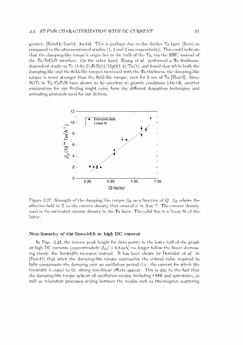
3.5. ST-FMR CHARACTERIZATION WITH DC CURRENT 91
greater: [Kim13; Gar13; Avc14]. This is perhaps due to the thicker Ta layer (5nm) ascompared to the aforementioned studies (1, 3 and 3 nm respectively). This could indicatethat the damping-like torque's origin lies in the bulk of the Ta, via the SHE, instead ofthe Ta/FeCoB interface. On the other hand, Zhang et al. performed a Ta thickness-dependent study on Ta (1-5)/CoFeB(1)/MgO(1.3)/Ta(1), and found that while both thedamping-like and the eld-like torques increased with the Ta thickness, the damping-liketorque is never stronger than the eld-like torque, even for 5 nm of Ta [Zha13]. SinceSOTs in Ta/CoFeB have shown to be sensitive to growth conditions [Avc14], anotherexplanation for our nding might come form the dierent deposition techniques andannealing protocols used for our devices.
Figure 3.27: Strength of the damping-like torque βdl as a function of Q. βdl relates theeective eld in T to the current density that created it in A m−2. The current densityused is the estimated current density in the Ta layer. The solid line is a linear t of thelatter.
Non-linearity of the linewidth at high DC current
In Figs. 3.24, the inverse peak height for data points in the lower half of the graphat high DC currents (approximately |Idc| > 0.8 mA) no longer follow the linear decreas-ing trend: the linewidth increases instead. It has been shown by Demidov et al. in[Dem11] that when the damping-like torque approaches the critical value required tofully compensate the damping over an oscillation period (i.e., the current for which thelinewidth is equal to 0), strong non-linear eects appear. This is due to the fact thatthe damping-like torque acts on all oscillation modes, including FMR and spin-waves, aswell as relaxation processes arising between the modes such as two-magnon scattering
92 CHAPTER 3. SPIN-ORBIT TORQUES
[Hei85; Hur98; Len06], all of which lead to the increase of the linewidth. For the exper-iment shown in Fig. 3.24, we can extrapolate the DC current required to obtain a zerolinewidth, obtaining a critical current Icrit = 1.4 mA.
3.6 Conclusion
In this chapter we used ST-FMR spectroscopy to study Ta/FeCoB/MgO spin-wavewaveguides as a function of thickness to characterize the magnetic properties in absenceof DC current and the damping-like and eld-like torques in presence of DC current.To analyze the experimental results, in the rst part of this chapter we derived thesusceptibility equations using the concepts established in Sec. 1.2.5, considering dier-ent excitation schemes by dynamic Ørsted eld hø, eld-like hfl and damping-like hdl,generated by an RF current in the SWW. We then calculated the expected DC volt-ages generated by AMR and iSHE rectication to determine which components of thePolder susceptibility tensor contribute to the signal for dierent excitation schemes, aswell as the lineshape (symmetric Lorentzian or anti-symmetric dispersive) of each possi-ble signal. Based on this and the purely Lorentzian nature of the measured signals, weconcluded that the dominant source of DC signal in our SWWs is the combined action ofspin-pumping and the inverse Hall eect. Finally, we derived the shift of the resonanceeld by a static Ørsted Hø and static eld-like Hfl elds, as well as the reduction of thelinewidth via a static damping-like Hdl due to a DC current in the SWW.
In the second part of this chapter, we describe the FMR experiments using ourST-FMR setup. For Idc = 0 we extracted the eective magnetization Meff as a func-tion of thickness, allowing us to extract the saturation magnetization and the interfacialanisotropy constant, as well as the ferromagnetic layer critical thickness where the mag-netization reorients from in-plane to out-of-plane. We analyzed the eld linewidth ∆Hand qualitatively explained its unexpected variation as a function of thickness, in partic-ular, negative slopes of ∆H vs. the excitation frequency. This was accounted for by theinhomogeneous distribution of the saturation magnetization, the FeCoB thickness andthe anisotropy constant, which can be taken into account by only considering an inho-mogeneous distribution of the Q-factor that leads to a frequency-dependent contributionto the eld linewidth.
By performing ST-FMR experiments with the addition of a DC current , we carriedout a careful and systematic characterization of the eld-like and damping-like torquesof Ta/Fe72Co8B20/MgO vs. the ferromagnetic layer thickness, at the transition of themagnetization from in-plane to out-of-plane orientation, i.e., for Q-factors between ap-proximately 0.9 and 1.1. Firstly, we analyzed the shift in resonance eld and removedthe Joule heating contribution, and, taking the current distribution in the SWW andthe Ørsted eld into account, we extracted βfl, the ratio between the eective eld ofthe eld-like torque and the current density. The data shows that βfl and Q, i.e., theinverse of the FeCoB thickness, are linear, with some deviations around Q ≈ 1. Secondly,we analyzed the voltage peak height, which is inversely proportional to the linewidth,and extracted βdl, the ratio between the eective eld of the damping-like torque and

3.6. CONCLUSION 93
the current density, which was found to be proportional to the inverse of the FeCoBthickness. The absolute values of the eld-like torque βfl are comprised between 0 and5× 1014 T A−1 m2 depending on the ferromagnetic layer thickness, and values of thedamping-like torque βdl betweeen 2 and 10× 1014 T A−1 m2. Surprisingly, the damping-like torque is twice as strong as the eld-like torque in our devices for all FeCoB layerthicknesses, which is in contrast to most studies on similar systems. This might be ex-plained by the thicker Ta layer we used, which may enhance the SHE contribution of thebulk Ta to the damping-like torque.
Now that we have Now that we have demonstrated that SOTs can aect the k = 0uniform mode precession (resonance eld and linewidth) in Ta/FeCoB/MgO layers, andthat the iSHE can be used to detect the dynamic response, it will be of interest to seewhether SOTs can also aect propagating k 6= 0 spin-waves and whether the iSHE canbe used to detect them. The second aspect (detection via iSHE) will be the subject ofthe next chapter, while preliminary results on the rst aspect will be summarized in theConclusion and Perspectives.

94 CHAPTER 3. SPIN-ORBIT TORQUES

Chapter 4
Spin-wave excitation and detectionin Ta/FeCoB/MgO
In this chapter we present the detection of spin-waves in a Ta/FeCoB/MgO spin-wavewaveguide using the combined eect of spin-pumping and the inverse spin Hall eect.The spin-wave waveguides are the same as those studied in Chap. 3. We use a nano-metric coplanar waveguide (CPW) antenna to excite spin-waves within a large rangeof wavevectors. A rst task is therefore to calculate the expected spin-wave spectrumfor perpendicular magnetic anisotropy materials characterized by non-zero linewidth bytaking the geometry of the CPW antenna into account that will dene the spatial pe-riodicity of the excitation. The excitation is a convolution of the excitation eld andthe dynamic spin-wave susceptibility. We summarize the approach to obtain an expres-sion for the wavevector dependent excitation eciency of spin-waves and calculate theexpected spin-wave spectrum including also nite linewidth. The calculated spectrumis then compared to the experiments where the spin-waves are electrically detected viarectication due to the inverse spin Hall eect.
The results obtained using this detection technique, which we call spin-wave rec-tication spectroscopy (SWR), are also compared to Brillouin light scattering (BLS)experiments that were carried out at the university of Kaiserslautern by T. Brächerand myself. The BLS experiments furthermore allow us to determine the spin-wave de-cay length, and to extract the spin-wave lifetime. Finally, we discuss the merits of thespin-wave rectication technique with regards to device integration compared to otherdetection schemes.
The main ndings of this chapter were published in [Brä17b]. Thus, some text andgures have been adopted from the publication.
4.1 Material and device characterization
The spin-wave waveguides investigated in this chapter are described in Chap. 2, alongwith the details of their fabrication. A schematic of the device and the electrical contacts
95

96 CHAPTER 4. SPIN-WAVE EXCITATION AND DETECTION
is shown in Fig. 4.1.
Figure 4.1: Schematic of the spin-wave waveguide. A Ta/Fe72Co8B20/MgO trilayer ispatterned into a wire with leads to measure the voltage drop between A and B. AnAl2O3 layer insulates the SWW from the shorted coplanar waveguide on top that actsas a spin-wave excitation source. Taken from [Brä17b].
The SWWs are from the same wafer as those used for the ST-FMR experiments inChap. 3 that provided the materials properties and the strength of the damping-likeand eld-like torques. However the calculations and numerical simulations described inthis chapter were performed before the thickness-dependent material characterizationdescribed in Sec. 3.4 was completed, therefore there are some dierences in the materialparameters used to analyze the results here. This does however not aect the mainresults and conclusions presented.
The devices measured in this chapter are in-plane magnetized and have 0.85 < Q <0.90 (for the Q-factor see Eq. (3.61)). Due to the low Q-factor, in these devices theinhomogeneous contribution to the linewidth described in Sec. 3.4.4 is less importantand thus we are able to estimate the damping constant α, neglecting the inhomogeneousbroadening the damping via ST-FMR measurements (see Sec. 3.4.4). The values ofthe damping were averaged for all devices in this chapter, obtaining α = 0.019. Thevalue of the saturation magnetization used here, Ms = 1.25 MA m−1,1 is assumed basedon the study of Fe60Co20B20 in [Ver14]. Using this value, the interfacial anisotropyconstant is extracted from the measured eective magnetization Meff via the methoddescribed in Sec. 3.4.3, obtaining Ki = 1.18 mJ m−1. The exchange stiness constantAex = 10 pJ m−1 is assumed based on the study of Fe60Co20B20 in [Bel17]. These threeconstants, Ms, Ki and Aex, are parameters that govern the dispersion relation given inEq. (1.70), which is the basis of most of the calculations in this chapter. As such, slightlydierent values ofMs and Ki (which are linked byMeff , and is the most easily measuredparameter) would result in a dierent value of Aex and not greatly aect the calculations
1µ0Ms = 1.57 T.

4.2. VERIFICATION OF THE DISPERSION RELATION 97
and results of this chapter.In contrast to Chap. 3, in which devices are referred to by their Q-factor, in this
chapter the devices are mainly referred to by the CPW antenna design used to excitespin-waves (see Chap. 2). Moreover, it was shown in Chap. 3 that there is a nonGilbert-type damping present arising from the local inhomogeneities of the magneticproperties of the SWW, resulting in us being unable to properly determine the Gilbertdamping parameter. We carried out a separate ST-FMR analysis on the linewidth of thedevices measured in this chapter and obtained α = 0.019, assuming the entire dampingis Gilbert-type. This value was used for all calculations and simulations in this chapter.
4.2 Verication of the frequency-wavevector dispersion re-lation
In order to compare the spin-wave rectication experiments of Sec. 4.4 to the spin-wave eciency calculated in the subsections below, we need the frequency-wavevectordispersion relation. We gave an empirically obtained expression in Eq. (1.70) for a con-tinuous lm with PMA. To verify that the expression is also correct for the wires studiedhere, micromagnetic simulation were performed by T. Brächer using Mumax3.2 Thedetails of the simulations can be found in the supporting information of [Brä17b]. A dis-cretized ferromagnetic wire is modeled by 2048×256×1 cells (length×width×thickness),and the magnetization is excited by a localized Gaussian magnetic eld pulse. Two suc-cessive FFTs of the local magnetization as a function of time and space (i.e., cell position)yields data in the frequency-wavevector domain, from which the dispersion relation is ex-tracted. The results are presented in Fig. 4.2 for several values of anisotropy constants3
Eq. (1.70) was tted to the results. The good agreement of the t shows that the disper-sion relation given in Eq. (1.70) accurately predicts the numerical results given by thesimulations. Hence we can use the dispersion relation given in Eq. (1.70) to calculate thespin-wave eciency later in this chapter, as well as the group velocity and the relaxationrate.
2mumax3 is an open-source GPU-accelerated micromagnetic simulation program developed at theDyNaMat group of Prof. Van Waeyenberge at Ghent University. For more information, see [Van14] orvisit http://mumax.github.io/.
3In reality, all simulations were performed with the same number of cells and geometry. Instead ofvarying the anisotropy eld by varying the thickness, the anisotropy constant was varied for a xedthickness (i.e., the wire always has a thickness of 1 cell).

98 CHAPTER 4. SPIN-WAVE EXCITATION AND DETECTION
Figure 4.2: Squares: numerically simulated dispersion relation in a FeCoB SWW fordierent PMA constants Ki. Solid lines: dispersion relations calculated from Eq. (1.70)with the corresponding anisotropy constants. Taken from [Brä17b].
4.3 Excitation of spin-waves via coplanar waveguides
The aim of this section is to derive an expression of the spin-wave excitation in SWWusing a CPW in order to predict the expected spin-wave spectrum, that is experimentallymeasured in Sec. 4.4. In FMR and ST-FMR experiments, a spatially uniform excitation(magnetic eld or eective eld due to damping-like torque or eld-like torque, see Sec.3.2) is used to excite ferromagnetic resonance, which are non-propagative oscillationscharacterized by a wavevector k = 0. On the other hand, spin-waves are propagatingoscillations, with nite wavevector k 6= 0. Accordingly they are excited by spatiallynon-uniform magnetic elds, which one can characterize by their Fourier transform ink-space. A coplanar waveguide, through which an RF current ows, is an example of anantenna generating a non-uniform magnetic eld.
In this section, we calculate how eciently a CPW antenna at a given frequency andeld excites spin-waves in a certain wavevector range. The derivation of this eciencyinvolves obtaining an expression for the dynamic magnetization m of spin-waves underexcitation from the combination of (i) the CPW eld and (ii) the non-local dipolar eldgenerated by the spin-waves themselves. Since these calculations depend on having acorrect frequency-wavevector dispersion relation, we rst present in the subsection belowmicromagnetic simulations that allow us to verify that the dispersion relation given inEq. (1.70) is adequate. We then address in Sec. 4.3.1 the calculation of point (i) todetermine the spatial prole of the CPW eld. In Sec. 4.3.3 and 4.3.4 we address the

4.3. EXCITATION OF SPIN-WAVES VIA COPLANAR WAVEGUIDES 99
calculation of m considering both contributions as well as the nite linewidth. We thennumerically evaluate the derived expressions to predict the expected spin-wave spectrumfor the three coplanar waveguides (for details on the CPW designs, see Tab. 2.1).
4.3.1 Magnetic eld generated by a coplanar waveguide
The coplanar waveguides used in this work are composed of three parallel, thin wireswith a rectangular cross-section, as shown in Fig. 4.1. The CPWs are shorted at one end,and have contact pads at the other end for a ground-signal-ground RF probe; both theshort and the contacts are far away from the spin-wave waveguide. The CPW is on topof the SWW and perpendicular to the SWW axis so that the RF eld is oriented alongthe SWW long axis, see Fig. 4.1. A cross section of the CPW is shown in Fig. 4.3 alongwith the coordinate system. In this chapter, we will use only one coordinate system: x isthe out-of-plane axis, y is the long axis of the SWW and also the direction of propagationof the spin-waves, and z is the in-plane axis transverse to the SWW and parallel to thelong axis of the CPW. It is also the direction of equilibrium of the magnetization sincea magnetic DC eld is applied in this direction to saturate the magnetization.
Figure 4.3: Cross section of the coplanar waveguide antenna. The epitaxial Al2O3 layercovers the whole SWW and insulates it from the CPW. None of the thicknesses or widthsare to scale. The curved arrows represent the Ørsted eld created by the current I in theCPW wires. The eldH is applied parallel to the long axis of the CPW and perpendicularto the long axis of the SWW. When an RF current is injected in the CPW, the RF Ørstedeld excites spin-waves that propagate away from the CPW in either direction (purplearrows), and they can be detected via the iSHE by measuring the voltage between A andB.
When a current I is driven through the CPW, one can consider that the resultingmagnetic eld is the sum of the magnetic eld of each conducting wire. The expression

100 CHAPTER 4. SPIN-WAVE EXCITATION AND DETECTION
of the magnetic eld created by a current in a conductor with a rectangular cross sectioncan be calculated using the Biot-Savart law.4 Such a derivation can be found in [Chu06].We give the expressions of the magnetic eld components generated by the central wire,called the signal line, at a point (x, y) in space outside of the wires:
Hwirex = − I
8πab
[+ (b− x)
[1
2ln
((b− x)2 + (a− y)2
(b− x)2 + (−a− y)2
)+a− yb− x
arctan
(b− xa− y
)− −a− y
b− xarctan
(b− x−a− y
)]+(b+ x)
[1
2ln
((−b− x)2 + (a− y)2
(−b− x)2 + (−a− y)2
)+
a− y−b− x
arctan
(−b− xa− y
)− −a− y−b− x
arctan
(−b− x−a− y
)]](4.1)
Hwirey = − I
8πab
[+ (a− y)
[1
2ln
((b− x)2 + (a− y)2
(−b− x)2 + (a− y)2
)+b− xa− y
arctan
(a− yb− x
)− −b− x
a− yarctan
(a− y−b− x
)]+(a+ y)
[1
2ln
((b− x)2 + (−a− y)2
(−b− x)2 + (−a− y)2
)+
b− x−a− y
arctan
(−a− yb− x
)− −b− x−a− y
arctan
(−a− y−b− x
)]](4.2)
where x is the position along the out-of-plane axis and y is the position along the SWW'slong axis; 2a and 2b are the width and the thickness of the signal line and I is thecurrent owing through it. Since the current ows from the central signal line to the twoadjacent wires, called ground lines (see Figs. 4.1 and 4.3), the currents in the latter havethe opposite sign. Thus, the eld generated by each ground line can be found by takingEqs. (4.1) and (4.2) and replacing a and b by a′ and b′, I by −I2 , and performing thevariable change: y′ = y ± s, where s is the center-to-center spacing between the signalline and the ground lines, and the plus or minus sign indicates which ground line is beingcalculated: the one to the left or the one to the right of the signal line. Then, the totalmagnetic eld created by the CPW at a given position in the SWW is simply the sumof these 3 terms.
We present in Fig. 4.4 the components of the total magnetic eld, calculated as afunction of the distance y along the SWW, at a xed position x below the center ofthe CPW, x = 54.5 nm, which corresponds to the surface of the ferromagnetic layer in
4We assume that the wire is innitely long.

4.3. EXCITATION OF SPIN-WAVES VIA COPLANAR WAVEGUIDES 101
our experiments.5 The CPW design used in the example of Fig.4.4 is type C, whichhas 2a = 70 nm wide wires with s = 150 nm center-to-center spacing, and thickness2b = 30 nm.
Figure 4.4: In-plane eld component µ0Hcpwy (blue) and out-of-plane eld component
µ0Hcpwx (orange) created by a CPW, 54.5 nm below the center of the CPW. The eld
components are calculated according to Eqs. (4.1) and (4.2), for lines with width 2a =70 nm, thickness 2b = 30 nm and center-to-center spacing s = 150 nm. The rectanglesdrawn in black represent the cross section of the CPW. Each curve is normalized to themaximum of the blue curve.
Let us make several remarks. Firstly, all CPWs are composed of 30 nm Au and 5 nmTi. Additionally, bulk Ti is 20 times more resistive than bulk Au and the true resistivityof the Ti layer is expected to be even larger given its thickness and the interface with theunderlying alumina layer. Thus, we treat the Ti as non-conductive in the calculation ofthe magnetic eld due to its lower thickness and its higher resistivity.
Secondly, the Biot-Savart equation is valid for magnetostatics, but here the aim isto inject an RF current in the GHz range and thus one would expect the Biot-Savartequation to be inadequate for this purpose. However, it has been shown in [Heu15] vianumerical calculations that the Biot-Savart equation gives a good approximation of thestrength of the magnetic eld even at frequencies in the GHz range.
Finally, at high frequencies in thick enough conductors, the electric current owsmainly within the skin depth of the conductor. This is due to eddy currents induced bythe changing magnetic eld caused by the alternating current. The skin depth is givenby:
δ =
√ρ
πfµrµ0(4.3)
where ρ = 22.2 nΩm and µr = 1 are the bulk resistivity and relative permeability of Au,
5The calculated depth corresponds to: 15 nm of Au (half of the total Au), 5 nm of Ti, 30 nm epitaxialAl2O3, 2 nm Al2O3, 1 nm Ta2O5, and 1.5 nm MgO.

102 CHAPTER 4. SPIN-WAVE EXCITATION AND DETECTION
and f = 6 GHz is the upper bound of the frequency used in the experiments describedin this chapter. The resulting skin depth is δ = 0.97 µm, which is much larger than thethickness and width of the conducting lines of the CPWs.
Thus, we take the magnetostatic elds calculated via Eqs. (4.1) and (4.2) to be validfor RF currents up to the GHz range. As shown in Fig. 4.4, the CPW gives rise toa symmetrical in-plane eld, parallel to the long axis of the SWW, which reaches itsmaximum amplitude under the center of the CPW. On the other hand, the out-of-planeeld is anti-symmetrical, vanishes under the center of the CPW and then changes sign,reaches its maximum amplitude under each ground line.
From the spatial prole in Fig. 4.4 we obtain the Fourier spectrum of an antenna'smagnetic eld, shown in Fig. 4.5. Since we are performing numerical calculations, thedata is non-continuous and we use a fast Fourier transform (FFT) algorithm to calculatethe Fourier spectrum of the magnetic eld for all three CPW designs. An interestingproperty of the magnetic eld of a given CPW is that the absolute value of the FFTof the in-plane and of the out-of-plane components are equal. The elds are calculatedas per Fig. 4.4: at a depth 54.5 nm below the center of the wires, which correspondsto the surface of the ferromagnetic layer; and as a function of y. Therefore the Fouriercoecients, written bky for either eld component, are expressed as a function of ky, thewavevector component parallel to the direction of propagation y, and they constitute theFourier spectrum of the CPW, written (bky).
6
Moreover, the Fourier spectra of all the CPW designs (A, B, C) show a similar prole:the rst maximum is the highest, each following maximum is notably smaller than theprevious one, and the amplitude is zero between maxima. More importantly, the minimaare situated at integer multiples of 2π
s , where s is the center-to-center spacing. Conse-quently, the smaller s is, the larger is the range of wavevectors between two minima. Infact, if one uses a single wire, a design called stripe antenna, there is only one maximum,at ky = 0, and the amplitude decreases to 0 for increasing wavevectors [Ciu16]. On theother hand, the width 2a only has an inuence on the maximum amplitudes of the curvebetween the minima.
Thus we have designed nanometric CPW antennae for the purpose of exciting a largerange of non-zero wavevectors. These antennae are scalable not only because one canreduce their size and spacing and still obtain elds capable of exciting spin-waves, butalso because this reduction leads to shorter wavelengths, which is a basic requirementfor scaling down any magnonic device to the nanometer scale. Moreover, the wavevectordependent spin-wave excitation of the CPWs will allow us to characterize the iSHEdetection scheme by comparing the expected spectrum vs. the measured signal, anddetermine whether the iSHE detection is wavevector independent or not.
6(bky ) refers to the Fourier spectrum, while bky refers to a specic Fourier coecient of this spectrum.

4.3. EXCITATION OF SPIN-WAVES VIA COPLANAR WAVEGUIDES 103
Figure 4.5: Absolute value of the FFT of the magnetic eld components created by threedierent CPW designs, assuming a xed current. CPW type A: in-plane (black line)and out-of-plane component (blue dots). CPW type B: in-plane (red line) and out-of-plane component (dark red dots). CPW type C : in-plane (green line) and out-of-planecomponent (dark green dots). Each curve is normalized to the maximum of the blackline curve. For details about the CPW designs, see Tab. 2.1. The blue arrows show theminima detected in the spin-wave rectication experiments for CPW A (dashed blue)and CPW B and C (solid blue). The red arrow shows the minimum of the spectrumclose to the minimum detected in the Brillouin light scattering microscopy experimentfor CPW B.
4.3.2 Spatial prole of spin-waves in a spin-wave waveguide in theDamon-Eshbach conguration
We remind the two main congurations for spin-wave excitation that were describedin Sec. 1.3.3: the backward volume conguration, where the saturating external eld isapplied parallel to the direction of propagation, and the Damon-Eshbach conguration,where the eld is applied in-plane but transversely to the direction of propagation. In thischapter, we will mainly deal with the Damon-Eshbach conguration, thus the calculationswill be done in that geometry.
We consider the Damon-Eshbach conguration, with a propagation of spin-wavesin the y direction and the magnetization saturated through a magnetic eld along thez direction. Here we summarize the expressions for the components kx, ky, kz of thecorresponding wavevector k. Dierent waveguide modes can be excited, each with adierent spatial conguration in the (x, z) plane due to the nite size, analogous to thevibration modes of a drum membrane.

104 CHAPTER 4. SPIN-WAVE EXCITATION AND DETECTION
In the x direction, perpendicular to the lm, according to Sec. 1.3.3, the ferro-magnetic layer is thin enough that the spin-waves present an homogeneous prole acrossthe thickness of the lm, with kx = 0 as higher modes require much higher excitationfrequencies.
The SWW is half a µm to several µm wide, which is small enough to induce quanti-zation of the width mode, described by the width or waveguide mode number n. Thus,spin-wave modes of dierent proles can exist along the z direction, described here bythe mode number n and kz = (n+1)π
ww. In the Damon-Eshbach conguration, the magne-
tization at the lateral edges of the SWW can be aligned with the external eld (the edgesare unpinned) or aligned with the long axis of the SWW (the edges are pinned) as wellas anywhere in between. This is due to the competition between the Zeeman energy andthe dipolar energy, and it can lead to an inhomogeneous eective eld, which is reducednear the edges. In such a case, one can dene an eective width weff as the width of theSWW where the eective eld is greater than half the external eld. For more detailson the calculation see [Brä15]. In our case, we determined using Eq. (2.56) in [Brä15]:
Heff (z) = H − Ms
π
(arctan
(tf
2z + ww
)− arctan
(tf
2z − ww
))(4.4)
that weff ≈ ww for the 5 µm wide SWW. This means that the magnetization at thelateral edges of the SWW are pinned and parallel to the edges.
Finally, ky, the wavevector component parallel to the propagation direction, is con-tinuous.
4.3.3 Excitation eciency
Now that we have calculated the magnetic eld created by the three CPW designs,we can look at the spin-waves they can excite. Interestingly, the amplitude of the FFTfor all three CPWs for ky = 0 is zero, a characteristic of CPWs. This means that an RFeld generated by the CPWs is incapable of exciting ferromagnetic resonance, which hask = 0.
As mentioned before, the aim is to have an expression for the excitation eciency,where the excitation eld has two contributions. In the previous section we consideredthe eld from the CPW, but one also has to consider the dynamic dipolar eld generatedby the SWs themselves that is obtained from the spatial prole of the spin-waves. Thisinvolves solving the equation of motion for the spin-wave magnetization as was done in[Sch08] for the Damon-Eshbach and the backward volume congurations.7 Here we willsummarize the main steps for the Damon-Eshbach conguration.
The propagation of spin-waves is aected by the dipolar eld created by the spin-waves themselves. Therefore, the relation in Eq. (1.21) becomes, for spin-waves:
m = χ (h + hd) (4.5)
7Further reading may include [Kal80; Gus02; Kos07; Dem09].

4.3. EXCITATION OF SPIN-WAVES VIA COPLANAR WAVEGUIDES 105
where h is the excitation eld generated by the CPW, hd is the spin-wave dipole eldand χ is the susceptibility tensor for the uniform mode excitation (see Eq. (1.29) in Sec.1.2.4). The dipolar eld can be written as [Sch08]:
hd(y) =
∫ +∞
−∞G(y − y′)m(y′)dy′ (4.6)
where G is a 2D tensorial Green's function. The Green's function for magnetostatics isdetailed in [Gus02]. It describes the dipolar eld at a point y created by the magnetizationat a point y′, and the integration over the ferromagnet gives the total dipolar eld at theposition y. The elements of the tensorial Green's function are related to the componentsof the susceptibility tensor for uniform magnetization dynamics using Eq. (4.6). Onecan rewrite Eq. (4.5) as an expression relating the magnetization to the uniform modesusceptibility components. In the Damon-Eshbach conguration, this is given by [Sch08;Dem09]:
mx(y, t) =4π
tf|bky |
χ⊥ − sign(ky)
χ2⊥ − χ2
‖eikyyeiωt (4.7)
where mx is the out-of-plane component of the magnetization, tf is the thickness of theferromagnetic layer, y is the position of the spin-wave along the direction of propagation,ky the component of the wavevector parallel to the direction of propagation, χ‖ and χ⊥are the diagonal and o-diagonal components of the susceptibility tensor in Eq. (1.29),|bky | is the amplitude of the Fourier transform of the CPW eld for the wavevector ky,presented in Sec. 4.3.1, and ω is the angular frequency of the excitation eld.
In Eq. (4.7), both the in-plane and the out-of-plane components of the CPW's eldare taken into account, though their combined eect on the spin-wave depends on itsdirection of propagation, given by sign(ky).8 Indeed, as seen in Fig. 4.4, the magneticeld components have the same sign under the left ground line while they have oppositesign under the right ground line. Due to the well-dened direction of rotation of themagnetization, the torques of the two components of the RF eld on the magnetizationare in phase on one side of the antenna, and out of phase on the other side of it. Theresult is an asymmetry of the amplitude of the spin-waves depending on the propagationdirection. Thus, spin-waves with ky > 0 have greater amplitude than spin-waves withky < 0.
The amplitude of dynamic magnetization oscillation |m| at a given wavevector ky isa measure of how eciently a spin-wave at ky is excited and provides the wavevectorresolved spin-wave spectrum as it can be measured in an experiment. We thereforedene the excitation eciency here η ∝ |m|. For a thin lm system with perpendicularanisotropy, the excitation eciency is written [Brä17b]:
η±n (ky) = |bz,n||bky |∣∣∣∣fn(ky)
µ0γ′± 1
µ0Meff
(fn(ky)
2
γ′2− µ2
0H2eff
)∣∣∣∣ (4.8)
8If bky,hx is the Fourier transform of the out-of-plane eld as a function of y, and bky,hy is the Fouriertransform of the in-plane eld as a function of y, then through symmetry arguments and using Maxwell'sequations, Schneider et al. found that bky,hx = i sign(y) bky,hy [Sch08].

106 CHAPTER 4. SPIN-WAVE EXCITATION AND DETECTION
where ± indicates whether ky > 0 or ky < 0, fn(ky) is the frequency of the spin-wavewith ky and n indicates the waveguide mode n due to the quantication of kz acrossthe width of the SWW, see Sec. 4.3.2.9 γ′ is the gyromagnetic ratio in GHz T−1, Meff
is the eective magnetization dened in Eq. (1.14), Heff is the eective eld in theferromagnetic layer as dened in Eq. (1.12). The bz,n factor is proportional to the nettorque that the RF elds can exert on the magnetization for a given waveguide mode n.Therefore, bz,n is proportional to the net integrated magnetic moment across the eectivewidth:
bz,n ∝1
n+ 1cos
[π(n+ 1)(z +
deff2
)
] deff2
deff2
=
1
n+1 forn even
0 forn uneven(4.9)
As a result, uneven-numbered modes cannot be excited in the Damon-Eshbach geometry,and waveguide modes of increasing number n have an excitation eciency that decreaseswith 1
n+1 .10
In the model described thus far, if one excites a SWW with a CPW, a certain rangeof wavevectors can be excited, depending on the spatial features of the CPW. However,due to the dispersion relation, the choice of applied frequency and exernal static eld willselect only one wavevector. Additionally, only uneven waveguide modes can be excited,and one direction of propagation will be favored. The asymmetry of the spin-wave'samplitude as a function of propagation direction can be a desired property for someapplications, for example spin-wave logic gates in which information must pass only inone direction.
4.3.4 Non-zero linewidth model
The eect of relaxation processes on spin-waves was not discussed in the derivation ofthe excitation eciency Eq. (4.8). In this subsection, we include the non-zero linewidthin the excitation eciency as derived by T. Brächer and P. Pirro in [Brä17b]. Phe-nomenological losses in magnetization dynamics lead to a non-zero frequency linewidth,which can be linked to the relaxation rate given in Eq. (1.71), via:
∆fn(ky) =ωrπ
(4.10)
where ∆fn(ky) is the linewidth in units of frequency for the spin-wave frequency fn(ky).A consequence of the non-zero frequency linewidth is that the spin-waves with ky can beexcited not only at frequencies fn(ky) but also at frequencies close by f ′ 6= fn(ky). The
9The frequency and the wavenumber are related by the dispersion equation (1.70) for a FeCoB thinlm system with perpendicular anisotropy. It is therefore a function of kx, ky and kz; however sincekx = 0 and kz has discrete values depending on n, we write the spin-wave frequency as fn(ky) for easeof reading.
10In other works in the literature, such as [Dem09; Brä17a; Brä17b], the mode index starts at n = 1for the fundamental mode, and thus in that numbering scheme only uneven modes can be excited andtheir eciency decreases with 1
n. We started the index at n = 0 for the fundamental mode due to the
lack of nodes in its prole, similarly to [Wan].

4.3. EXCITATION OF SPIN-WAVES VIA COPLANAR WAVEGUIDES 107
distribution of the frequencies f ′ of the spin-waves with a given wavevector ky excited atfn(ky) is given by a Lorentzian function [Hei94]:
Lky(f′) =
2
π
∆f2n(ky)
4 [f ′ − fn(ky)]2 + ∆fn(ky)2
(4.11)
This Lorentzian function is dened such that∫ +∞−∞ Lky(f
′) df ′ = 1 to reect its property asa probability density. To account for all of the spin-waves with wavevector component kyand waveguide mode n, excited by a source generating a magnetic eld at a frequency f =fn(ky), we calculate the excitation eciency of Eq. (4.8) by the frequency distributiondue to the non-zero linewidth:
c±n (f ′, ky) = η±n (ky)× Lky(f ′) (4.12)
In the following we will numerically evaluate the expression in Eq. (4.12) to predict theexcitation spectrum that we expect to measure in a wavevector independent experimentsuch as the spin-wave rectication for which only the frequency of the excitation sourceis swept continuously. For this we have to integrate Eq. (4.12) over all wavevectors toobtain an expression of the excitation eciency C±n (f ′) as a function of the excitationfrequency f'. In the numerical evaluations, due to discretization this will be a sum overky:
C±n (f ′) =∑ky
c±n (f ′, ky) (4.13)
Next we describe the procedure for the evaluation of C±n (f ′). Using the disper-sion relation given in Eq. (1.70), we substitute the variable ky by fn(ky) and calculatec±n (f ′, fn(ky)) for f ′ and fn(ky), with both variables ranging from 0 to 10 GHz in steps of1 MHz. In the resulting 2D matrix, where the values of c±n (f ′, fn(ky)) as a function of f ′
(and xed fn(ky)) are stored in the columns, a summation over the rows gives the totalexcitation eciency C±n (f ′) in the presence of non-zero linewidth, for a given waveguidemode n and for a xed external eld H.
We present in Fig. 4.6 the normalized excitation eciency C±n (f ′), calculated for allthree CPW designs, under a DC eld µ0H = 55 mT. The unnormalized data show a largedierence in amplitude. To better compare, in Fig. 4.6 we normalized each excitationeciency to its respective maximum. We compare the excitation eciency C±n (f ′) takinginto account only the waveguide mode n = 0 (solid lines) and when taking into accountthe modes with n up to n = 4 (dotted lines). As can be seen, the inuence of the n = 2and n = 4 modes is negligible for all three CPW designs, and for all frequencies in theexplored range. This is due to the fact that while the width of the SWW is small enoughfor quantization of the waveguide modes, it is large enough that the mode separation interms of frequency is small, and therefore the excitation prole changes little betweenmodes. Additionally, the amplitude of each higher mode decreases with 1/(n+ 1). Thus,for all further calculations, we ignore the eects of the higher order waveguide modesn > 0.

108 CHAPTER 4. SPIN-WAVE EXCITATION AND DETECTION
Figure 4.6: Normalized excitation eciency of the three CPW designs for a xed magneticeld µ0Heff = 55 mT and for an eective magnetization µ0Meff = 194 mT. The solidlines are the calculations including only the fundamental mode n = 0, the dotted linesinclude all modes up to n = 4. Each curve is normalized to its respective maximum.
Additionally, it is clear that we are far from exciting a single spin-wave with a givenwavevector component and its associated frequency. The combination of the large rangeof wavevectors that the CPW antenna can excite, and the non-zero linewidth leads to acomplex excitation eciency with several peaks of varying amplitude, as shown in Fig.4.6.
4.4 Spin-wave rectication experiments
4.4.1 Experimental setup
The experimental setup for spin-wave rectication spectroscopy (SWR) is somewhatsimilar to the one used for the ST-FMR experiments in Chap. 3: an electromagnetsupplies a uniform magnetic eld that is slowly varied. The setup, shown in Fig. 4.7(see also Figs. 4.1 and 4.3) for SWR measurements uses a similar principle than ST-FMR but with the important dierence that the RF current is not applied to the SWWbut to the CPW antenna fabricated on top. As described in Sec. 4.3 this will excitespin-waves of non-zero wavevector (see Fig. 4.6), and the experiment can thus provideinformation on the propagating spin-waves. For their excitation, high-frequency probesare connected to nanometric shorted CPWs on top of the SWWs. A signal generatorsupplies a high frequency current in the GHz range, which is modulated in power at a

4.4. SPIN-WAVE RECTIFICATION EXPERIMENTS 109
frequency in the 10 kHz range via a lock-in amplier (LIA). The LIA is connected to theleads of the SWWs. It is used to detect the voltage rectied via iSHE which arises fromthe resulting spin-wave dynamics in the FeCoB. In the SWR experimental geometry, themagnetization is oriented along the short axis of the SWW by the external eld. Thismaximizes the iSHE signal, as will be discussed in Sec. 4.4.3.
Figure 4.7: Schematic of the spin-wave rectication setup. An electromagnet generatesa magnetic eld H perpendicularly to the long axis of the SWW. A signal generatorsupplies the CPW antenna with an RF current which is modulated at fmod by the lock-in amplier. The lock-in amplier measures the iSHE voltage between A and B.
Like in the ST-FMR measurements, the rectied voltage is detected as a functionof the applied eld for a given excitation frequency. The applied power of -1 dBmcorresponds to the regime of linear excitation, whereas an increase of the power by about2-3 dB leads to a deviation of the linear scaling of the measured voltage with the appliedmicrowave power.
4.4.2 Measurement protocol
A sinusoidal RF current, set at constant frequency throughout the measurement, issent through the CPW antenna. The electromagnet is set such that the eld will be inthe plane of the device at an angle θH = 90 with respect to the long axis of the SWW,as shown in Fig. 4.1. The magnetic eld is then decreased down to a minimum of µ0H =−170 mT, sweeping across the resonance and then decreased back to 0. The measurementis then immediately repeated for positive elds. The DC voltage is measured across theSWW Au contacts, with the signal-to-noise ratio enhanced via the modulation of the RFpower and the lock-in amplier.
Unlike ST-FMR experiments, the result of SWR is not a Lorentzian peak. When theeld is swept, it excites a continuous range of spin-waves, resulting in one or more non-Lorentzian peaks, depending on the CPW design used. Thus, the linewidth cannot be

110 CHAPTER 4. SPIN-WAVE EXCITATION AND DETECTION
characterized. The results are then compared to the expected excitation proles obtainedvia the calculations derived in Sec. 4.3.
Linearity with respect to RF power
As with the ST-FMR experiments (see Sec. 3.4.1), we seek to study spin waves in thelinear excitation regime, which we characterize by the proportionality between the squareof the resonance peak voltage and the RF power injected in the CPW. Of course, we aresimultaneously exciting a continuum of spin-waves with a certain range of wavevectors,and thus cannot compare two spin-wave resonance peaks individually. Thus, we plot thelogarithm of the maximum voltage of the measured spin-wave spectrum as function of theRF power injected in the CPW, shown in Fig. 4.8. In the resulting log-log plot, the lineart is adequate until a power threshold of about −1 dBm. Thus the SWR experimentsare performed at this power or below. Unfortunately, the BLS experiments described inSec. 4.5 were carried out before we could determine the linearity power threshold.
Figure 4.8: Maximum voltage of the spin-wave spectrum as a function of the RF powerinjected in the CPW antenna. The linear t on the log-log scale shows the linearitythreshold at approximately −1 dBm.
4.4.3 Angle dependence of spin-wave rectication
We performed an angle-dependent measurement of the spin-wave rectication, simi-larly to the ST-FMR measurements by varying the in-plane eld angle θH similarly to theexperiment described in Sec. 3.4.2 for ST-FMR. From the spin-wave spectra we extract
4.4. SPIN-WAVE RECTIFICATION EXPERIMENTS 111
the maximum amplitude and plot the results as a function of the in-plane angle of theeld in Fig. 4.9.
There are some key dierences with ST-FMR. Firstly, the spin-wave excitation is theresult of two eld components, an in-plane one and an out-of-plane one (see Fig. 4.4).In the case of uniform FMR, the angle dependences for AMR and iSHE for these eldcongurations have been calculated in [Har16].11 We summarize their ndings here:
V xishe ∝ sin θH
V yishe ∝ sin θ3
H
V xamr ∝ sin(2θH)
V yamr ∝ sin(2θH) sin θH
(4.14)
where V xishe is the signal generated by the out-of-plane CPW eld excitation via the iSHE,
V yamr is the signal generated by the longitudinal CPW eld excitation via AMR, and θH
is the in-plane angle of the external eld.In the experiments described in this chapter we deal with spin-waves, therefore the
signals obtained may deviate from these results. As one rotates the electromagnet in theplane of the thin lm, the geometry changes from the Damon-Eshbach conguration tothe backward-volume conguration periodically meaning that, as shown in Fig. 1.4(b),the dispersion relation continuously shifts from one curve to the other.12 As seen in Eq.(4.8), the excitation eciency of a CPW antenna depends on the frequency and thereforeon the dispersion relation. Hence the spectrum of the excited spin-waves is expectedchange as a function of the angle as well. In Fig. 4.9, we only plot the maximumamplitude of the spectra as a function of the angle, and we are not able to take intoaccount the change in dispersion relation due to the angle.
As seen in Fig. 4.9, the angular dependence of the maximum voltage of the excitedspin-wave spectrum is well tted by a linear combination of V x
ishe and V yishe from Eq.
(4.14), and cannot be tted adequately by V xamr or V
yamr. This allows us to conclude that
the SWR signal in the SWW due to AMR is negligible, and that the combined eectsof spin-pumping and the iSHE are the dominant source of the signal. Furthermore, theexperiments presented in this chapter are performed at 90, an angle for which the AMRsignal is minimum, while the iSHE is maximum.
As mentioned for the ST-FMR case in Sec. 3.4.2, the Nernst eect, which has a cos θHdependence on the applied eld angle [Sch12], can also be dismissed. This is likely due tothe extremely small thickness of the FM layer, which likely has a negligible temperaturegradient.
4.4.4 Experimental results
In the following, we address the excitation and detection of propagating spin-waveswith non-zero wavevectors in spin-wave rectication (SWR) experiments and we showthat this technique allows for the wavevector independent detection of the locally excitedspin-wave dynamics in a large wavevector range. In the SWR experiment, the CPWs
11In [Har16], the rectication voltages for AMR can be found in Tab. 4 and the voltages for the iSHEin Tab. 6.
12Here, θk = θH .

112 CHAPTER 4. SPIN-WAVE EXCITATION AND DETECTION
Figure 4.9: Angle dependence of the spin-wave rectication signal. The maximum voltageof the detected spin-wave spectrum is plotted vs. the applied eld angle θH (blacksquares). The solid curves are the calculated angle-dependence of the iSHE voltages,given in Eq. (4.14), tted to the experimental data.
are used to excite propagating spin-waves and the rectied DC voltage arising from thedriven spin-wave dynamics is measured by the leads at the edges of the SWW. Thereforethe excitation as a function of the spin-wave wavevector is determined by the spatialextent of the excitation source, which is shown in reciprocal space in Fig. 4.5. TheSWWs are magnetized along their short axis to maximize the torque from the in-planeOersted eld created by the CPWs, in the Damon-Eshbach conguration.
Experimental results of the spin-wave rectication (SWR) measurements are shownin Fig. 4.10 for all three CPW designs A, B and C (see Tab. 4.1). Each device hasa dierent CPW design and a a dierent FM layer thickness and therefore a dierenteective magnetization. The characteristics of the 3 devices are resumed in Tab. 4.1.13
The three CPW designs gives access to dierent wavevector ranges (see Fig. 4.5).The SWR voltage due to spin-pumping and the iSHE is proportional to the square ofthe dynamic magnetization m2 (see Eq. (1.80)), and thus to the square of the spin-waveexcitation eciency calculated in Sec. 4.3.3. The measurements have been performedwith an applied RF power of P = 800 µW = −1 dBm at a frequency of 4.8 GHz. Thevoltages have been normalized to their individual maximum, which is on the order of µV.Further details on the absolute values of the measured voltages are given in a subsectionbelow.
As can be seen in Fig. 4.10 the spin-wave rectication spectra vs eld for f = 4.8 GHz
13The devices investigated in this section are 7-C1, 7-D1 and 7-E1 in Tab. 2.2.

4.4. SPIN-WAVE RECTIFICATION EXPERIMENTS 113
Figure 4.10: Measured spin-wave intensity spectra (solid lines) and analytical calculationsof the expected excitation spectra (dashed lines), at a xed frequency of 4.8 GHz, for3 dierent CPW designs and eective magnetizations. Black lines: CPW type A andµ0Meff = 168 mT. Red lines: CPW type B and µ0Meff = 194 mT. Green lines: CPWtype C and µ0Meff = 221 mT (See Tab. 4.1 for details on the CPWs). The shadedpeaks show the ST-FMR peaks of each spin-wave waveguide, colored correspondingly.All measured voltages and calculated spectra have been normalized to their respectivemaximums for comparison. The blue arrow shows the approximate eld value where thecalculated spectra fall below the noise level of the measurement.
(full lines) show one large peak, with a subsidiary peak in some cases. The dashed linesrepresent the square of the spin-wave excitation eciency calculated via Eq. (4.13). Forcomparison, the ST-FMR peaks of the same devices are shown (shaded peaks). Thewidth of the SWR peaks as well as the eld separation between the SWR peaks andthe FMR peak increase as the distance s between the signal line and ground lines of theCPWs decrease. This is because the smaller CPWs excite a wider range of wavevectors,centered around a higher wavevector component ky, as predicted by Fig. 4.5.
Using the analytical formalism presented in Sec. 4.3, we determine the spin-wavespectrum in the SWWs. Taking into account the perpendicular magnetic anisotropy, thenon-zero linewidth, an eective width of the SWW of weff = 5 µm, we calculate theexpected spin-wave intensity spectrum excited by the CPWs, which is proportional tothe square of the excitation eciency calculated in Eq. (4.13) and shown in Fig. 4.6.They are represented by the dashed lines in Fig. 4.10, plotted as a function of appliedeld instead of applied frequency.
We average over the two emission directions along the wire, which are not equal due to

114 CHAPTER 4. SPIN-WAVE EXCITATION AND DETECTION
Table 4.1: Characteristics of the SWW used for the spin-wave rectication experiments.Each device has a dierent CPW design and a dierent FM layer thickness. The devicesare referred to by their CPW design.
CPWdesign
2a (nm)wire width
s (nm)wire spacing
µ0Meff
(mT)A 120 500 168B 70 300 195C 70 150 221
the interplay of the in-plane and out-of-plane component of the CPW eld, as describedby the ± symbol in Eq. (4.8). Furthermore, we only consider the fundamental waveguidemode n = 014 in the calculations since the inuence of higher modes is negligible as shownin Fig. 4.11. The analytical calculations assuming a wavevector independent detectioneciency by the iSHE are in good agreement with the experimentally obtained spectra.The small visible deviations are likely caused by a too simple description of the material'sdamping, which is assumed to be entirely Gilbert-type,15 and by an idealization of theCPWs which neglects their edge roughness.
The calculated intensity drops close to the noise level of our experimental setup forµ0H ≈ 52 mT. We convert this eld value into a wavevector for each device via Eq.(4.13),16 obtaining a dierent value for each CPW design. Thus, the calculated intensitydrops to the noise level of the setup for wavevectors beyond the third minimum of theCPWs of type A, beyond the second minimum for type B and beyond the rst minimumfor type C (see the blue vertical arrow in Figs. 4.5 and 4.10). This eld value corre-sponds to approximately 40 rad µm−1 for all three types of CPWs and is equivalent to awavelength of λ = 166 nm for type A and of λ = 150 nm for type B and C, because theminima are situated at integer multiples of 2π
s , where s is the center-to-center spacingof the CPWs. The experimentally accessible wavevector range and the envelopes of themeasured spectra are predominantly determined by the features of the excitation sourceand no systematic discrepancy with increasing wavevector is observed. Thus, the detec-tion eciency via iSHE is independent of the spin-wave wavevector in the experimentallyaccessible wavevector range.
To demonstrate the feasibility of the iSHE detection for a broader range of frequencies,Fig. 4.11 compares the measured excitation spectra of the three dierent CPW types tothe corresponding expected excitation spectra for frequencies between 2 and 5.5 GHz,determined by the available eld range of our experiments. The measured voltage andthe expected spin-wave intensity are displayed color-coded as a function of the applied
14We remind that in other works, the fundamental width mode can be referred to as n = 1.15In Sec. 3.4.4, we qualitatively characterize a non-Gilbert-type damping in ST-FMR experiments,
caused by a inhomogeneous eective magnetization of the ferromagnetic layer. This non-Gilbert-typedamping is also present in the devices used in this section but has not been characterized.
16For each device, we calculate Eq. (4.13) for µ0H = 52 mT and f = 4.8 GHz and using the device'sMeff and its CPW design. We sum over the rows to account for the non-zero linewidth, and look upthe corresponding wavevector.

4.4. SPIN-WAVE RECTIFICATION EXPERIMENTS 115
eld and frequency. The white lines correspond to the Kittel ts obtained from the ST-FMR measurements. The spectra have been normalized individually to their maximumat each frequency to account for the changes of the input impedance. All color mapsuse an identical, logarithmic scale. As can be seen from Fig. 4.11, the measured spectraare in good qualitative agreement in the probed eld and frequency range. In the entirerange, the noise-limited maximum detectable wavevector is about 40 rad µm−1 and isdetermined by the Fourier spectrum of the excitation source. The visible small peak atelds larger than the FMR, which corresponds to a spin-wave mode below the spin-waveband, is associated with an edge mode, [Gub04] which is weakly excited by the CPW.
Figure 4.11: Color-coded measured and calculated spin-wave intensities as a function ofthe applied frequency and applied magnetic eld. Both have been normalized to theirrespective maximum for a given frequency. The upper panel shows the measurement andthe lower panel the analytical calculations. (a): CPW type A and µ0Meff = 168 mT.(b): CPW type B and µ0Meff = 194 mT. (c): CPW type C and µ0Meff = 221 mT.The white lines represent the Kittel ts obtained from the ST-FMR measurements. Inboth panels, the dashed lines are guides to the eye indicating the position of the maximaof the spectra expected from the calculations. Taken from [Brä17b].

116 CHAPTER 4. SPIN-WAVE EXCITATION AND DETECTION
Comparison of measured voltages
In the following paragraphs, we provide a more quantitative analysis of the ampli-tude of the iSHE signals. In order to check whether there is a dependence of the iSHEvoltage level on the excited wavevector itself we compare the voltage levels for the dif-ferent types of CPW that have their rst maximum at dierent wavevectors. The peakvoltages for the dierent CPW antennae obtained in the experiments are: CPW typeA: Vmax = (13.2± 1.3) µV, CPW type B: Vmax = (2.5± 0.3) µV, and CPW type C:Vmax = (1.1± 0.1) µV. The ratio between the voltages for each CPW, [C:B:A], is thus[(1) : (2 ± 1) : (12 ± 2)]; the error following from assuming a 10% uncertainty in thevoltages arising from the variations in the contacting and the device resistance. Theseexperimental values are compared to calculations from Sec. 4.3. These are determinedby three factors:
In the following we will try to estimate the expected voltage ratios between thedierent CPWs, which are determined by three factors:
1. The Fourier spectrum of the CPWs: Fig. 4.12 shows the square of the Fourierspectrum of the three CPWs normalized to CPW type C. This corresponds to therelative excitation amplitude which is expected if the current sent into the CPWs iskept xed. It corresponds to a dierent voltage ratio [C:B:A] of [1:2.7:4.1] betweenthe dierent CPWs.
2. The dierent transmission characteristics of the CPWs: for a xed microwave cur-rent, the peak values of the microwave elds created by all three CPWs are thesame within ±10%, so we assume them to be equal for simplicity. The CPWs oftype B and C feature identical resistances, typically around 550Ω; devices of typeA feature a twice larger track width and, thus, a twice smaller resistance, typi-cally around 275Ω. Assuming that due to the very small size of the structures incomparison to the microwave wavelength the impedance is essentially determinedby the resistance, this results in a larger reection from CPW B and C than fromCPW A. The transmission coecient of the antennae is related to the reexioncoecient given in Eq. (3.57):
T = 1− Γ =2× 50
Rcpw + 50(4.15)
whereRcpw is the resistance of the considered CPW design and the source impedanceof the signal generator is 50Ω. The ratio of the transmission coecient for CPWA over the transmission coecient for CPW B and C is 1.85, thus we have acontribution of [1:1:1.85].
3. The excitation volume of the CPWs: given that the FM layer is ultra-thin andthat all of the antennae designs feature CPWs that extend over the whole widthof the SWW, we can consider that the excited SWW thickness tf and width ww(see Fig. 4.3) is equal for all CPW designs. However the width of the signal andground lines are not equal among the CPW designs: type B and C feature three 70

4.5. BRILLOUIN LIGHT SCATTERING EXPERIMENTS 117
nm wide lines whereas type A features 120 nm wide lines and, hence, the excitedSWW length is 120/70 ≈ 1.71 times larger. The iSHE voltage is proportional tothe excited volume, therefore this leads to an increase of the expected iSHE voltagefor CPW type A by a factor of 1.71, leading to [1:1:1.71].
Figure 4.12: Square of the absolute value of the FFT of the eld created by the CPWantennae. Black line: CPW type A. Red line: CPW type B. Green line: CPW type C.
Multiplying these 3 contributions together, the expected voltage ratio is [1:2.7:13], whichis in very good agreement with the experimentally obtained ratio [(1) : (2±1) : (12±2)].We can conclude that the ratio is determined by the experimental setup and that theiSHE voltage level does not depend on the excited wavevector, within the experimentallyaccessible wavevector range, and within the range of frequencies explored in Fig. 4.11.
4.5 Brillouin light scattering experiments
In the previous section, we successfully detected magnetization dynamics via theiSHE rectication eect. To prove that we are measuring propagating spin-waves, weperformed micro-focused Brillouin light scattering (BLS) experiments. Additionally, weare interested in characterizing the propagation of the spin-waves, which is possible withspatially resolved BLS microscopy, for two reasons. Firstly, to characterize the decaylength of the spin-waves and thus their lifetime. Secondly, to verify that the spin-wavesdetected via the iSHE are far away from the contacts, to show that the iSHE detectionscheme is sensitive to localized spin-waves dynamics.
118 CHAPTER 4. SPIN-WAVE EXCITATION AND DETECTION
Micro-focused Brillouin light scattering is an optical technique that allows the de-tection of local magnetization dynamics. We17 were given the opportunity to performmeasurements on our devices using a Brillouin light scattering microscope in the groupof B. Hillebrands at the State Research Center OPTIMAS at the Technical Universityof Kaiserslautern. Measurements were performed with the help of T. Meyer, T. Fischerand P. Pirro. The working principles of BLS, as well as a detailed description of themicroscope itself and of the measurement technique can be found in the dissertation ofT. Brächer [Brä15]. Alternatively, reviews on BLS microscopy can be found here [Seb15;Dem15]. In the following, we will only give a very brief overview.
4.5.1 Working principle
Brillouin light scattering is based on the interaction of light (photons) with oscillationsin a material. The nature of these oscillations can be acoustic (phonons), dielectric(polarons) or magnetic (magnons).18 The scattering of photons with magnons is inelastic,meaning that the energy of the photon is not conserved following the interaction withthe ferromagnetic material. However, the total energy of all particles involved in theinteraction is conserved:
hν ′ = hν ± hf(k) (4.16)
where h is Planck's constant, ν and ν ′ are the photon's frequency before and after thescattering process respectively and f(k) is the frequency of the interacting magnon withwavenumber k. During the scattering process, the photon can either create or annihilatea magnon (the creation of a magnon is illustrated in Fig. 4.13), which is represented bythe ± sign. Thus, the interaction of photons with magnons results in a frequency-shiftof the photons that is equal to the frequency of the detected spin-wave.
4.5.2 Description of the microscope
A schematic of the microscope is given in Fig. 4.14. A solid-state laser provides amonochromatic light source at a wavelength of 532 nm. The light is guided onto thesample by a microscope objective and focused down to a spot size of about 400 nm,with an eective spatial resolution of about 250 nm. Micro-step motors and an auxiliaryoptical microscope allow precise positioning of the spot on the sample's surface. Theinelastically scattered light is recollected by the objective and guided into a 3+3-passJRS Tandem Fabry-Pérot interferometer [Moc87] where it is analyzed with respect tofrequency and intensity. The obtained BLS intensity at a given frequency is proportionalto the number of inelastic scattering events of the light with magnons of this frequency inthe probing spot. Thus, it is directly proportional to the local spin-wave intensity underthe laser spot.
In addition to the change in energy described in Eq. (4.16), the photon also experi-ences a change in momentum. In the simplied case where the magnon's wavenumber is
17T. Brächer and I.18Following the concept of wave-particle duality, magnons are quantized spin-waves.

4.5. BRILLOUIN LIGHT SCATTERING EXPERIMENTS 119
Figure 4.13: Sketch of magnon-photon scattering processes. The incident photon withfrequency ν and wavevector ky,photon creates a magnon in the ferromagnetic layer withfrequency f(ky) and wavevector ky. The scattered photon has a reduced frequency ν ′ andreduced wavevector k′y,photon due to energy and momentum conservation. In the oppositeprocess, a magnon is annihilated by the incident photon, and the scattered photon hasan increased frequency and increased wavevector. Taken from [Brä15].
simply k = ky, y being the direction of propagation and along the axis of the SWW, wehave:
k′y,photon = ky,photon ± ky (4.17)
where ky,photon and k′y,photon are the photon's wavevector component parallel to y beforeand after the scattering, respectively. Since the reected light is collected by the samemicroscope objective that focuses the incident light, this change of wavevector has an im-portant consequence. The direction of propagation of a photon is given by its wavevector,which means that the interaction with a magnon changes the reected photon's direction.Since the objective has a limited aperture, a reected photon with too great a change inwavevector cannot be captured by the objective. In other words, such BLS microscopesare inherently limited by their optics and cannot detect spin-waves beyond a certainwavevector. The resolution limit of the microscope used in this work is 19 rad µm−1.
Unlike the ST-FMR experiments of Chap. 3 and the SWR experiments of Sec. 4, inthe BLS experiments presented in this section the applied eld is set to a xed value.There is no RF current or eld. The analysis of the scattered photons gives the spin-wavespectrum in the frequency domain.
4.5.3 BLS measurements
The BLS measurements are performed on a 2 µm wide SWW with a type B CPW,µ0Meff = 195 mT,19 in the Damon-Eshbach conguration: the SWW is magnetizedalong the short axis by a xed external magnetic eld. The microwave frequency is sweptat an applied power of 1.26 mW = +1 dBm. This is above the non-linearity threshold
19Device 8-D2 in Tab. 2.2.

120 CHAPTER 4. SPIN-WAVE EXCITATION AND DETECTION
Figure 4.14: Schematic of a Brillouin light scattering micro-focused microscope. Formore information, see the source [Brä15], Sec. 3.2.
identied in Fig. 4.8 for the ST-FMR experiment, which may not be accurate for theBLS experiments presented here. Non-linearities appear as kinks in the exponentialdecay length (see Sec. 4.5.4), which were not observed. Thus we assume that we arein the linear excitation regime. Fig. 4.15 shows the BLS intensity spectra measured ata distance of about 200 nm to the right edge of the CPW for µ0H = ±55 mT. Themeasured spectrum in the vicinity of the CPW is compared to the analytically expectedspin-wave excitation spectrum (dashed lines) calculated in Sec. 4.3, Fig. 4.6,20 and tothe spin-wave dispersion relation of the fundamental mode (dotted green line). Bothmeasurement and calculations have been normalized to the maximum intensity in theecient emission direction (in this case for positive magnetic elds). As can be seenfrom Fig. 4.15, the two eld polarities exhibit a strong asymmetry in terms of theoverall intensity, the ratio is approximately 10 to 1. The strong asymmetry is mediatedby the PMA together with the excitation characteristics of the CPW described by Eq.(4.8), owing to the dependence on the wavevector sign ±ky. The PMA decreases theellipticity of precession and this way increases the relative spin-wave excitation eciencyof the dynamic out-of-plane elds created by the CPWs [Sch08; Kos13]. Consequently,the interplay of the dynamic out-of-plane and the dynamic in-plane eld componentsbecomes more pronounced, which is responsible for the asymmetric emission of antennaein this geometry (see Sec. 4.3.3). Thus, the use of CPWs or similar excitation sourcesfor the spin-wave excitation in ultra-thin lms with large PMA results intrinsically in
20The BLS measurement gives access to the spin-wave intensity, which is proportional to the squareof the excitation eciency calculated in Fig. 4.6.

4.5. BRILLOUIN LIGHT SCATTERING EXPERIMENTS 121
a pronounced unidirectional emission. Therefore, this excitation non-reciprocity is afeature of the CPW excitation and not directly connected to the intrinsic non-reciprocityof the classical Damon-Eshbach waves [Gur96] (see Sec. 4.3.3).
Figure 4.15: Measured (solid line) and calculated (dashed line) spin-wave intensityspectra detected at a distance of about 200 nm to the right edge of the CPW forµ0H = ±55 mT. The dotted green line shows the dispersion relation of the funda-mental mode (right y-axis). The red arrows mark the BLS detection limit in terms ofspin-wave wavevector (ky ≈ 19 rad µm−1) as well as spin-wave frequency.
The calculation and experiments agree up to the rst minimum of the CPW excita-tion at ky ≈ 21 rad µm−1 (compare the red arrow in Fig. 4.15 and in Fig. 4.5). This isexpected because this minimum incidentally almost corresponds to the maximum wave-vector which can be detected by the micro-focused BLS setup ky ≈ 19 rad µm−1. Incontrast, the detection via the iSHE can eciently detect spin-waves with larger wave-vectors. Moreove, the position of the rst minimum and the cuto appear at the samefrequency for both emission directions, indicating the absence of a sizable Dzyaloshinskii-Moriya interaction (DMI) in our Ta/FeCoB/MgO. For systems consisting of layers of Taand FeCoB-based alloys, the presence [Tet15; Gro16] or absence [Sou16; Kha16; Sou16]of DMI is still debated.
4.5.4 Spin-wave decay length
We now seek to characterize the propagation length of the spin-waves in the SWW.Due to relaxation processes, the amplitude of the spin-wave decays exponentially as thewave propagates in the ferromagnetic material. We previously described the spin-waverelaxation rate ωr in Eq. (1.72), which is related to the spin-wave lifetime τ via ωr = 2π
τ .
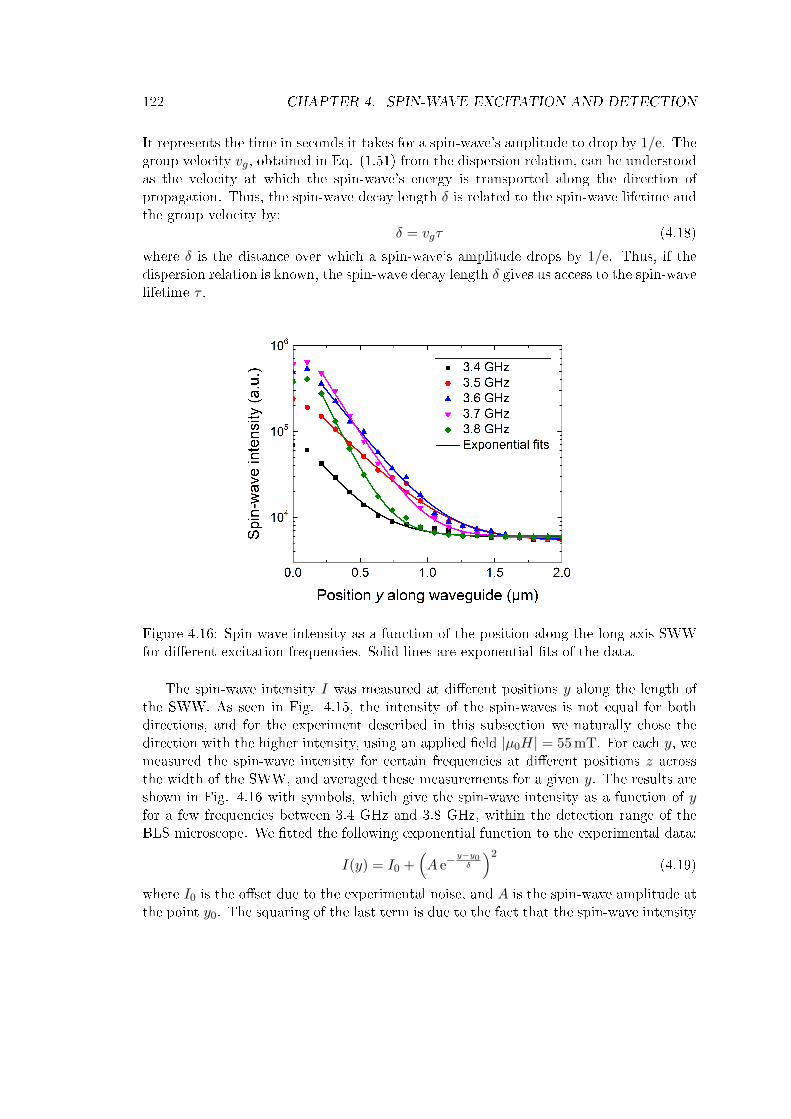
122 CHAPTER 4. SPIN-WAVE EXCITATION AND DETECTION
It represents the time in seconds it takes for a spin-wave's amplitude to drop by 1/e. Thegroup velocity vg, obtained in Eq. (1.51) from the dispersion relation, can be understoodas the velocity at which the spin-wave's energy is transported along the direction ofpropagation. Thus, the spin-wave decay length δ is related to the spin-wave lifetime andthe group velocity by:
δ = vgτ (4.18)
where δ is the distance over which a spin-wave's amplitude drops by 1/e. Thus, if thedispersion relation is known, the spin-wave decay length δ gives us access to the spin-wavelifetime τ .
Figure 4.16: Spin-wave intensity as a function of the position along the long axis SWWfor dierent excitation frequencies. Solid lines are exponential ts of the data.
The spin-wave intensity I was measured at dierent positions y along the length ofthe SWW. As seen in Fig. 4.15, the intensity of the spin-waves is not equal for bothdirections, and for the experiment described in this subsection we naturally chose thedirection with the higher intensity, using an applied eld |µ0H| = 55 mT. For each y, wemeasured the spin-wave intensity for certain frequencies at dierent positions z acrossthe width of the SWW, and averaged these measurements for a given y. The results areshown in Fig. 4.16 with symbols, which give the spin-wave intensity as a function of yfor a few frequencies between 3.4 GHz and 3.8 GHz, within the detection range of theBLS microscope. We tted the following exponential function to the experimental data:
I(y) = I0 +(A e−
y−y0δ
)2(4.19)
where I0 is the oset due to the experimental noise, and A is the spin-wave amplitude atthe point y0. The squaring of the last term is due to the fact that the spin-wave intensity

4.5. BRILLOUIN LIGHT SCATTERING EXPERIMENTS 123
is the square of the spin-wave amplitude. The exponential ts are performed only fory > 200 nm, suciently far from the CPW so that the laser spot is not partially on theCPW, which would distort the detected spin-wave intensity.
As can be seen in Fig. 4.16, the spin-wave intensity is highest near the CPW and itdecays exponentially along the SWW, indicating that the spin-waves are excited locallyby the CPW and propagate with losses. Because of the exponential decay of the spin-waves, the iSHE voltage is dominated by the dynamics of the spin-waves in the vicinityof the CPW.
Figure 4.17: Exponential spin-wave decay length as a function of applied frequency,extracted from spatially resolved BLS measurements at |µ0H| = 55 mT using Eq. (4.19).
In Fig. 4.17, we plot the spin-wave exponential decay length δ as a function offrequency. It initially increases with increasing frequencies up until approximately 3.45GHz and then the decay decreases with increasing frequencies. Around a frequency of3.45 GHz, δ reaches its largest value of about δ ≈ 600 nm. We compare this to the decaylength calculated from the dispersion relation in Eq. (1.70), by using the expressions ofthe relaxation rate in Eq. (1.71), the group velocity in Eq. (1.51), the decay length inEq. (4.18) as well as ωr = 2π
τ :
δ = vg2π
ωr
= 2π
∣∣∣∣∂ω(k)
∂k
∣∣∣∣ (αω∂ω(k)
∂ωH
)−1 (4.20)
Assuming the aforementioned values of α = 0.019 and µ0Meff = 195 mT for the devicewith CPW type B (see Tab. 4.1), the exponential decay length obtained is δ = 400 nm

124 CHAPTER 4. SPIN-WAVE EXCITATION AND DETECTION
at 3.45 GHz, which is in reasonable agreement with the experimentally measured valueabove.
Using Eq. (4.18), we calculate the spin-wave lifetime corresponding to the spin-wavedecay lengths in Fig. 4.17. The spin-wave lifetimes presented in Fig. 4.18 show amaximum value of around 3 ns close to 3.45 GHz. These values are comparable to the
Figure 4.18: Spin-wave lifetimes obtained from the experimentally measured spin-wavedecay lengths in Fig. 4.17 via Eq. (4.18).
ones obtained by micromagnetic simulations carried out by T. Brächer, presented in theSupporting Information of [Brä17b]. Based on the same Mumax3 model presented inSec. 4.2, the spin-wave lifetime is extracted from the same simulations. The lifetimesobtained from the simulations are presented in Fig. 4.19 for dierent values of theanisotropy constant. For comparison, the spin-wave lifetime calculated according to Eq.(1.72) is also shown for the same anisotropy constants.
The spin-wave lifetimes obtained by experiments, the analytical calculations and themicromagnetic simulations are all large in comparison to the values expected from amaterial system with similar values of Ms and α but no PMA. This can be understoodfrom the ellipticity contribution to the lifetime for the ferromagnetic resonance. TheFMR lifetime τfmr, in seconds, is given by [Hei94]:
1
τfmr= αγ′µ0
(H +
Meff
2
)(4.21)
A reduction of Meff due to the PMA signicantly increases the lifetime at low magneticelds where H ≈Meff . The experimentally obtained value of 3 ns is comparable to thelifetime in thicker ferromagnetic lms on the order of tens of nanometers from metallic

4.5. BRILLOUIN LIGHT SCATTERING EXPERIMENTS 125
Figure 4.19: Spin-wave lifetimes obtained via Eq. (1.72) (green lines) and by micromag-netic simulations (squares) for dierent values of interfacial anisotropy. The interfacialanisotropy measured in devices for this chapter is Ki = 1.18 mJ m−1. The importantspread of the results is due to the nite resolution in space (the number of cells thatcompose the simulated magnetic volume) and in time of the simulation model. Takenfrom [Brä17b].
materials such as NiFe [Bau15] or the half-metallic Heusler compound Co2Mn0.6Fe0.4Siin the absence of pronounced interfacial damping [Seb12].21
For slightly larger frequencies, above 3.45 GHz, the spin-wave lifetimes obtainedexperimentally in Fig. 4.18 shows an unexpectedly strong decrease in the short rangeof frequencies measured as compared to the numerically obtained lifetimes in Fig. 4.19.This potentially indicates the presence of a wavevector-dependent relaxation process inthe measured devices. This is not incorporated into the analytical formalism, which mightalso explain why the maxima/minima in the measured spectra are not as well resolved aspredicted. We recall that in the ST-FMR experiments described in Sec. 3.4.4, we founda frequency-dependent and thickness-dependent contribution to the linewidth, though itmanifests itself at lower frequencies and smaller FeCoB thicknesses than the ones usedhere.
21Heusler compounds are alloys which can present a unique mix of properties such as semi- or half-metallicity, ferro- or antiferromagnetism, low magnetic damping, etc. [Tru10].

126 CHAPTER 4. SPIN-WAVE EXCITATION AND DETECTION
4.6 Comparison of spin-wave detection methods
Ultimately, we would like to compare the iSHE detection to other detection methods:BLS detection (and other magneto-optical techniques like Kerr magnetometry) is localand the measured intensity depends on the local spin-wave density, which makes it avery powerful tool that does not require a large magnetic volume [Seb15; Dem15]. Inprinciple, it is possible to measure the phase-evolution of propagating spin-waves directlyby BLS, meaning that this method can give information on the wave amplitude and phasesimultaneously. In contrast, the maximum resolvable wavevector is quite low (aroundk = 19 rad µm−1 for the microscope used in this chapter), which does not suce to studythe short-waved spin-waves of interest for future magnonic applications. In addition,the limitations by optical diraction also limit the usefulness of BLS for nanoscopicstructures. The optical setup makes it a good tool for laboratory work but will bedicult to implement in actual magnonic devices integrated on chips. For this electricalexcitation and detection schemes are required.
For the detection of spin waves, we can use also use antennae (CPWs and other de-signs) in a reciprocal eect as discussed here for excitation of spin-waves. Such inductivetechniques are used in many laboratories and can be integrated on a chip. However theycan only give information about the spin-wave phase if costly microwave equipment likevector network analyzers or ultrafast oscilloscopes are used [Bai03]. In addition, induc-tive antennae exhibit a strong wavevector selectivity given by their Fourier spectrum.22
Furthermore, the weak inductive coupling between the antenna and the dynamic mag-netization limits the applicability of inductive detection to microscopic devices; theirsensitivity is insucient for nanoscopic structures. Because it scales with the magneticvolume, inductive detection are less suited for miniaturized structures made from ultra-thin lms or lms with low magnetization.
In contrast, the iSHE detection excels in such layer systems as shown here: iSHEdetectors can be easily integrated on a chip and show enough sensitivity and signal-to-noise ratio. The iSHE scales with the length over which spin-waves propagate, whereasinductive detection scale with the size of the antenna used. If only thin metallic layers areinvolved, the iSHE voltage is not shunted and is straightforward to detect. In contrast,in thick ferromagnetic layers, the iSHE voltage is reduced due to shunting eects andother phenomena, such as thermal eects arising from an inhomogeneous heating ofthe magnetic layer that can dominate the electric signal. As shown in the experimentsdescribed here, the iSHE detection limit is at least k = 40 rad µm−1 (determined by theexcitation antenna used), though there is nothing in the detection mechanisms leading tothe DC voltage that suggests that there is an intrinsic limit to the range of wavevectorsdetectable by the iSHE. The same holds true for the wavevector-independence of thistechnique. Thus, it is an ideal detection method for the development of scalable magnonicdevices which calls for the reduction of the spin-wave wavelengths used. However, the
22The Fourier spectrum that gives an antenna's spin-wave excitation prole (see Sec. 4.3.1) alsogives its spin-wave detection prole, making antennae an intrinsically wavevector-dependent detectiontechnique.
4.7. CONCLUSION 127
iSHE detection can, by itself, always only provide amplitude and no phase information.Thus, the phase must be converted into another type of information, for instance, bytranslating it into an amplitude information [Brä16].
The studied spin-wave rectication experiment is similar to the thermoelectric detec-tion in [Sch12], in which spin-waves propagate in a 100 nm thick NiFe SWW. Insteadof the iSHE, spin-waves are detected via the anomalous Nernst eect (ANE). The decayof magnons create a temperature gradient which is detected as a voltage drop via theANE. Such a detection technique is also expected to have no limit in wavelength andto be wavevector-independent. However, as shown in Sec. 4.4.3, we did not detect anysignicant ANE signal, which is likely due to the fact that the FM layer in our devicesis so thin that a thermal gradient is negligible. Thus, ANE detection is not suited forultrathin SWWs.
4.7 Conclusion
Using the model derived by T. Brächer and P. Pirro, we have calculated the completespectrum of the spin-wave excitation eciency of the coplanar waveguides, taking intoaccount the perpendicular anisotropy of the Ta/FeCoB/MgO system and the non-zerolinewidth of the spin-waves.
We detected propagating spin-waves presenting a large range of wavevectors up to≈ 40 rad µm−1 via the inverse spin Hall eect for several devices and CPW designs.Furthermore, the wavevector dependence that can be observed (the maxima and minimaof the spectra) as well as the upper limit of detectable wavevector can be exclusivelyattributed to the excitation scheme using CPW antennae. Hence it is concluded thatiSHE is wavevector independent and can be used for detecting spin-waves in a muchlarger range of wavevectors.
By performing Brillouin light scattering experiments on the same spin-wave wave-guides, we conrmed that the voltage generated by iSHE is due to propagating spin-waves, and that the iSHE is capable of detecting spin-waves localized far away fromthe where the DC signal is measured. A strong asymmetry was measured between thespin-waves propagating in either direction away from the CPW, which was predicted bythe spin-wave excitation eciency. This is due to the interplay between the in-plane andout-of-plane RF eld of the CPW and is not related to the non-reciprocity of the classicalDamon-Eshbach waves or to the Dzyaloshinskii-Moriya interaction, which is shown to beabsent in the Ta/FeCoB/MgO material system.
Using BLS, we measured the spin-wave decay length in Ta/FeCoB/MgO, allowing usto calculate the spin-wave lifetime. We obtained a lifetime that is comparable to systemswith relatively low intrinsic damping, due to the role of the perpendicular magneticanisotropy in the Ta/FeCoB/MgO system, in which the demagnetizing eld is almostcompensated by the PMA eld.
To conclude, the Ta/Fe/MgO system with strong PMA investigated here, togetherwith the iSHE detection technique, are compatible with the integration into conventionalmicroelectronics, owing to the compatibility of the material deposition and fabrication

128 CHAPTER 4. SPIN-WAVE EXCITATION AND DETECTION
techniques, and the fact that the iSHE voltage naturally arises in any bilayer systemwhere a FM and a NM with a signicant spin Hall angle share a large interface. Addi-tionally, the iSHE detection scheme is an ideal candidate for scalable magnonic devices,as its wavevector sensitivity shows no indication of an upper limit nor any wavevectordependence, allowing the reduction of the device size and the wavelength used. Moreover,the chosen material system allows the manipulation of spin-waves with a simple electriccurrent via the spin-orbit torques demonstrated in Chap. 3. Finally, the Ta/FeCoB/MgOstack is also compatible with other spintronic technologies such as MRAM, which arealready commercialized. This paves the way for the development of scalable wave-basedlogic devices integrated onto CMOS electronics, with the possibility of including STT-MRAM or newer generation SOT-MRAM for fast, non-volatile memory.

Conclusion and perspectives 129
Conclusion and perspectives
This thesis addresses the applicability of a Ta/FeCoB/MgO slab with an ultrathinferromagnetic layer and characterized by a strong PMA, as a spin-wave waveguide. Inparticular, we focused on the characterization of the spin-orbit torques with the aim ofusing them to manipulate spin-waves as well as the capacity of the inverse spin Hall eectto provide a wavevector independent method of detecting spin-waves.
The rst experimental chapter is dedicated to the characterization of the magneticproperties of Ta/FeCoB/MgO spin-wave waveguides via spin-torque ferromagnetic res-onance. The expected voltages arising from this technique were calculated, taking intoaccount the dierent RF excitation sources as well as the two possible rectication mech-anisms. It was concluded that in our spin-wave waveguides the main source of the DCsignal is the combined eects of spin-pumping and the inverse spin Hall eect, and thatanisotropic magnetoresistance rectication is negligible. Due to the lineshapes of thesignals generated by the inverse spin Hall eect, it was impossible for us to dierentiatebetween Ørsted eld, eld-like torque or damping-like torque excitations. However, thisdoes not mean that measuring the spin-orbit torques via ST-FMR is impossible. Indeed,we derived the modications to the susceptibilities induced by a DC eld-like torqueand a DC damping-like torque, both produced by a DC current injected in the SWW.Following an analysis of the linewidth of the resonance peak as well as its resonanceeld as a function of the injected DC current, we characterized βfl (respectively βdl),the ratio between the eective eld of the eld-like (respectively damping-like) torqueand the current density in the Ta layer. From the characterization as a function offerromagnetic layer thickness, we concluded that both βfl and βdl increase as the ferro-magnetic layer thickness decreases, which is consistent with the fact that βfl and βdl areinversely proportional to the volume, i.e. the thickness.
Before analyzing the DL and FL torque as a function of current and ferromagneticlayer thickness, we performed an analysis at Idc = 0 and extracted the eective mag-netization as a function of ferromagnetic layer thickness, which governs the balance be-tween the demagnetization energy and the perpendicular magnetic anisotropy energy,determining the orientation of the magnetization. We identied the critical thicknessof reorientation and studied devices around and at the transition. The extraction ofthe damping proved to be more complicated than expected, as an unexpected variationof the eld linewidth ∆H vs. the excitation frequency appeared for many devices. Wequalitatively explained this result, particularly the negative slope of the linewidth vs. the

130 Conclusion and perspectives
excitation frequency by taking into account an inhomogeneous distribution of the mag-netic properties of the ferromagnetic layer, resulting in a non-linear frequency-dependentcontribution to the eld linewidth.
The second experimental chapter is devoted to the excitation, propagation and de-tection of spin-waves in the same Ta/FeCoB/MgO spin-wave waveguides. The excitationspectrum of the nanometric coplanar waveguides was calculated, taking into accountthe perpendicular magnetic anisotropy as well as the non-zero linewidth of the spin-waves. Taking advantage of the same detection mechanism that was demonstrated inTa/FeCoB/MgO for uniform (k = 0) modes in the previous chapter, we performed spin-wave rectication experiments. By comparing the measured spin-wave spectrum to thecalculated excitation spectrum, we concluded that the detection mechanism is wavevectorindependent up to a wavevector of at least 40 rad µm−1, at which value the signal dropsbelow the noise level. This value corresponds to minima for the excitation by the coplanarwaveguides, hinting that the iSHE-based detection method is eective and wavevectorindependent even for higher wavevectors.
The spin-wave rectication experiments were complemented by Brillouin light scatter-ing microscopy, conrming that the detected signal arises from propagating spin-waves.We then measured the spin-wave intensity as a function of distance from the coplanarwaveguide and extracted the spin-wave decay length, which allowed us to calculate thespin-wave lifetime. We found a spin-wave decay length of 600 nm and a spin-wave life-time of approximately 3 ns, which is comparable to the lifetime of thicker NiFe systemswhich lack a pronounced interfacial damping. The large lifetime is attributed to the per-pendicular anisotropy of the Ta/FeCoB/MgO, which reduces the eective magnetizationand its contribution to the ellipticity, leading to a reduced lifetime.
In comparison to other spin-wave detection methods such as BLS and inductive cou-pling, the main advantage of the iSHE method used in this work is its wavevector-independence. More importantly it can be directly integrated with the device and themeasurement requires no extensive laboratory equipment: the spin-wave dynamics isconverted to a charge current, which can be detected by a transistor for example. Addi-tionally, it shows no limit in terms of scalability, in terms of nanofabrication or wavelengthlimit. Of course, it lacks an important feature, namely that it cannot measure the phaseof a spin-wave.
The next logical step is therefore combining the two main concepts studied in thiswork: spin-orbit torques and spin-waves. By injecting a DC current in the waveguidewith the correct polarity, the damping-like torque can reduce the eective damping of thesystem, enhancing the lifetime of the spin-waves. We present in Fig. 4.20 preliminaryresults in which the voltage of the highest peak of the measured spin-wave spectrumis plotted as a function of the DC current injected longitudinally in the SWW. An RFcurrent with f = 4.8 GHz is supplied to the CPW antenna for several values between 0and -12 dBm, while the applied eld is swept across the resonance. In this conguration,a negative DC current is expected to enhance the eective damping, while a positiveone is expected to reduce it. Surprisingly, for both current polarities, the peak heightincreases as the current magnitude increases. In fact the eect is more pronounced for

Conclusion and perspectives 131
Figure 4.20: Spin-wave rectication experiment with DC current injected in a 1µm wideSWW, at f = 4.8 GHz. The voltage of the highest peak is plotted as a function ofapplied DC current. Each curve corresponds to a dierent RF power injected in theCPW antenna.
negative currents, which is contrary to our expectations. In Fig. 4.21, we plot the peakvoltage as a function of the power applied to the CPW antenna, for ±0.5 mA and ±1 mA.Since the power is in dBm, and the voltage scale is in logarithm, this is a log-log plot.Thus, the linearity between the measured voltage (which is related to the square of thedynamic magnetization) and the applied power is straightforward to verify. We see thatfor positive currents, the voltage is linear up to at least −2 dBm, while for negativecurrents, the voltage is non-linear for values starting at −8 dBm. Additionally, we seethat doubling the positive current does not result in signicant changes, while doublingthe negative current changes the non-linearity threshold and changes the slope of thelinear t.
We were unable to explain both the very high increase of the peak for currentsexpected to increase the eective damping (negative currents), nor the lack of eect onthe peak for currents expected to decrease the eective damping (positive currents). Inany case, the decrease of the nonlinear threshold for negative currents shows that forone polarity, there is a clear increase in nonlinear relaxation processes. It would beinteresting for future work to address these questions, as the enhancement of spin-wavesvia spin-orbit torques was achieved in dierent material and geometric congurations[Dem14; Che16], including nanowires [Dua14] similar to our SWWs. In these studies, theexcited magnetic volume is much reduced, resulting in the separation of the spin-wavemodes such that at a given excitation frequency, only one mode may exist, and therefore,

132 Conclusion and perspectives
Figure 4.21: Spin-wave rectication experiment with DC current injected in a 1 µm wideSWW, at f = 4.8 GHz. The voltage of the highest peak is plotted as a function of powerapplied to the CPW antenna. Up-pointing triangles correspond to positive currents, anddown-pointing triangles correspond to negative currents. The solid lines are partial linearts of the data.
only one mode can be excited by the spin-orbit torques. Thus, one can expect that insuciently narrow Ta/FeCoB/MgO, spin-waves enhanced by spin-orbit torques mightreach propagation lengths of several µm, paving the way for the development of metallicmagnonic devices that were previously only demonstrated in YIG, as well as their scalingdown to nanometric sizes to contend with CMOS logic.

Appendix A
Linewidth and peak height under aDC damping-like torque
In this section we verify that for the iSHE signal, the inverse peak height of theresonance is proportional to the eld linewidth. Using the expression of the susceptibilityunder a DC damping-like torque derived in Eq. (3.20) in Sec. 3.2.4, we calculate ∆H ×Peak height, where ∆H is the linewidth and Peak height is the amplitude at resonanceof the real and imaginary parts of each susceptibility components.1 They are plotted asfunction of normalized current density in Fig. A.1. The current density is normalizedby the critical current, which is dened as the current density for which the linewidthis reduced to zero. For Re(χxy), the product of peak height and linewidth increaseswith J due to the DC damping-like torque (see Eq. (3.20)). However compared to theamplitudes of the other terms, which are constant as a function of J , this increase is small.Thus, when we consider the iSHE voltages in Eq. (3.55), we expect that the mixing of theo-diagonal and diagonal components of the susceptibility results in Lorentzian peaks inwhich the linewidth and the inverse peak height can be approximated as proportional.
1We usedMs = 1.25 MA m−1,Ki = 1.18 mJ m−1, tf = 1.35 nm, α = 0.02, βdlPz = 5 × 10¹⁴ T A−1 m2.
133

134 APPENDIX A. LINEWIDTH UNDER A DC DAMPING-LIKE TORQUE
Figure A.1: Product of the peak height and the linewidth, where the Peak heightand ∆H are calculated for each susceptibility component's real and imaginary part:∆H(χkl) × Re(χkl) and ∆H(χkl) × Im(χkl), for kl = xx, xy, yy. For the imaginaryparts of χxx and χyy, the lines are superimposed because they have dispersive lineshapesand thus their amplitude at resonance is zero. The current density J is normalized tothe critical current density Jc.

Bibliography
[All15] G. Allen, S. Manipatruni, D. E. Nikonov, M. Doczy, and I. A. Young. Exper-imental Demonstration of the Coexistence of Spin Hall and Rashba Eects inβtantalum/ferromagnet bilayers. Physical Review B 91, 14 (2015).doi: 10.1103/PhysRevB.91.144412.
[And09] K. Ando, J. Ieda, K. Sasage, S. Takahashi, S. Maekawa, and E. Saitoh. ElectricDetection of Spin Wave Resonance Using Inverse Spin-Hall Eect. AppliedPhysics Letters 94, 26 (2009).doi: 10.1063/1.3167826.
[And08] K. Ando, Y. Kajiwara, S. Takahashi, S. Maekawa, K. Takemoto, M. Takatsu,and E. Saitoh. Angular Dependence of Inverse SpinHall Eect Induced bySpin Pumping Investigated in a Ni81Fe19/Pt Thin Film. Physical Review B78, 1 (2008).doi: 10.1103/PhysRevB.78.014413.
[And11] K. Ando, S. Takahashi, J. Ieda, Y. Kajiwara, H. Nakayama, T. Yoshino, K.Harii, Y. Fujikawa, M. Matsuo, S. Maekawa, and E. Saitoh. Inverse Spin-Hall Eect Induced by Spin Pumping in Metallic System. Journal of AppliedPhysics 109, 10 (2011).doi: 10.1063/1.3587173.
[Ash69] H. Ashworth, D. Sengupta, G. Schnakenberg, L. Shapiro, and L. Berger. Gal-vanomagnetic Eects, Magnetostriction, and Spin-Orbit Interaction in Cu-Ni-Fe and Other Ferromagnetic Nickel Alloys. Physical Review 185, 2 (1969).doi: 10.1103/PhysRev.185.792.
[Avc14] C. O. Avci, K. Garello, C. Nistor, S. Godey, B. Ballesteros, A. Mugarza,A. Barla, M. Valvidares, E. Pellegrin, A. Ghosh, I. M. Miron, O. Boulle, S.Auret, G. Gaudin, and P. Gambardella. Fieldlike and Antidamping Spin-Orbit Torques in as-Grown and Annealed Ta/CoFeB/MgO Layers. PhysicalReview B 89, 21 (2014).doi: 10.1103/PhysRevB.89.214419.
[Aze11] A. Azevedo, L. H. Vilela-Leão, R. L. Rodríguez-Suárez, A. F. Lacerda Santos,and S. M. Rezende. Spin Pumping and Anisotropic Magnetoresistance Volt-ages in Magnetic Bilayers: Theory and Experiment. Physical Review B 83, 14
135

136 BIBLIOGRAPHY
(2011).doi: 10.1103/PhysRevB.83.144402.
[Bai88] M. N. Baibich, J. M. Broto, A. Fert, F. N. Van Dau, F. Petro, P. Eti-enne, G. Creuzet, A. Friederich, and J. Chazelas. Giant Magnetoresistanceof (001)Fe/(001)Cr Magnetic Superlattices. Physical Review Letters 61, 21(1988).doi: 10.1103/PhysRevLett.61.2472.
[Bai03] M. Bailleul, D. Olligs, and C. Fermon. Propagating Spin Wave Spectroscopyin a Permalloy Film: A Quantitative Analysis. Applied Physics Letters 83, 5(2003).doi: 10.1063/1.1597745.
[Bak84] A. Bakun, B. Zakharchenya, A. Rogachev, M. Tkachuk, and V. Fleisher. Ob-servation of a Surface Photocurrent Caused by Optical Orientation of Elec-trons in a Semiconductor. JETP Lett 40, 11 (1984).url: http://www.jetpletters.ac.ru/ps/1262/article_19087.shtml.
[Bau15] H. G. Bauer, P. Majchrak, T. Kachel, C. H. Back, and G. Woltersdorf. Non-linear Spin-Wave Excitations at Low Magnetic Bias Fields. Nature Commu-nications 6 (2015).doi: 10.1038/ncomms9274.
[Bea07] J.-M. Beaujour, W. Chen, K. Krycka, C.-C. Kao, J. Z. Sun, and A. D. Kent.Ferromagnetic Resonance Study of Sputtered Co|Ni Multilayers. The Euro-pean Physical Journal B 59, 4 (2007).doi: 10.1140/epjb/e2007-00071-1.
[Bel17] M. Belmeguenai, D. Apalkov, Y. Roussigné, M. Chérif, A. Stashkevich, G.Feng, and X. Tang. Exchange Stiness and Damping Constants in DilutedCoxFeyB1-x-y Thin Films. Journal of Physics D: Applied Physics 50, 41 (2017).doi: 10.1088/1361-6463/aa81a5.
[Ber04] D. Bercioux. Spin-Dependent Transport in Nanostructures, PhD thesis. Uni-versità degli studi di Napoli Federico II, 2004.url: http://www.fedoa.unina.it/136/1/masterthesis.pdf.
[Ber64] L. Berger. Inuence of Spin-Orbit Interaction on the Transport Processes inFerromagnetic Nickel Alloys, in the Presence of a Degeneracy of the 3d Band.Physica 30, 6 (1964).doi: 10.1016/0031-8914(64)90105-3.
[Ber70] L. Berger. Side-Jump Mechanism for the Hall Eect of Ferromagnets. PhysicalReview B 2, 11 (1970).doi: 10.1103/PhysRevB.2.4559.
[Ber96] L. Berger. Emission of Spin Waves by a Magnetic Multilayer Traversed by aCurrent. Physical Review B 54, 13 (1996).doi: 10.1103/PhysRevB.54.9353.

BIBLIOGRAPHY 137
[Bil07] C. Bilzer, T. Devolder, P. Crozat, C. Chappert, S. Cardoso, and P. P. Fre-itas. Vector Network Analyzer Ferromagnetic Resonance of Thin Films onCoplanar Waveguides: Comparison of Dierent Evaluation Methods. Journalof Applied Physics 101, 7 (2007).doi: 10.1063/1.2716995.
[Bin89] G. Binasch, P. Grünberg, F. Saurenbach, and W. Zinn. Enhanced Magnetore-sistance in Layered Magnetic Structures with Antiferromagnetic InterlayerExchange. Physical Review B 39, 7 (1989).doi: 10.1103/PhysRevB.39.4828.
[Boz42] R. M. Bozorth and D. M. Chapin. Demagnetizing Factors of Rods. Journalof Applied Physics 13, 5 (1942).doi: 10.1063/1.1714873.
[Brä17a] T. Brächer, O. Boulle, G. Gaudin, and P. Pirro. Creation of UnidirectionalSpin-Wave Emitters by Utilizing Interfacial Dzyaloshinskii-Moriya Interac-tion. Physical Review B 95, 6 (2017).doi: 10.1103/PhysRevB.95.064429.
[Brä17b] T. Brächer, M. Fabre, T. Meyer, T. Fischer, S. Auret, O. Boulle, U. Ebels,P. Pirro, and G. Gaudin. Detection of Short-Waved Spin Waves in IndividualMicroscopic Spin-Wave Waveguides Using the Inverse Spin Hall Eect. NanoLetters 17, 12 (2017).doi: 10.1021/acs.nanolett.7b02458.
[Brä16] T. Brächer, F. Heussner, P. Pirro, T. Meyer, T. Fischer, M. Geilen, B. Heinz,B. Lägel, A. A. Serga, and B. Hillebrands. Phase-to-Intensity Conversion ofMagnonic Spin Currents and Application to the Design of a Majority Gate.Scientic Reports 6 (2016).doi: 10.1038/srep38235.
[Brä15] T. Brächer. Parallel Parametric Amplication of SpinWaves in Micro-Structures.PhD Thesis. Technischen Universität Kaiserslautern, 2015.url: https://www.physik.uni-kl.de/fileadmin/hillebrands/Diplom-_und_Doktorarbeiten/PhD_Braecher.pdf.
[Byc84] Y. A. Bychkov and É. I. Rashba. Properties of a 2D Electron Gas with LiftedSpectral Degeneracy. Journal of Experimental and Theoretical Physics 39, 2(1984).url: http://www.jetpletters.ac.ru/ps/1264/article_19121.pdf.
[Che16] T. Chen, R. K. Dumas, A. Eklund, P. K. Muduli, A. Houshang, A. A. Awad,P. Dürrenfeld, B. G. Malm, A. Rusu, and J. Åkerman. Spin-Torque and Spin-Hall Nano-Oscillators. Proceedings of the IEEE 104, 10 (2016).doi: 10.1109/JPROC.2016.2554518.

138 BIBLIOGRAPHY
[Che93] V. Cherepanov, I. Kolokolov, and V. L'vov. The Saga of YIG: Spectra, Ther-modynamics, Interaction and Relaxation of Magnons in a Complex Magnet.Physics Reports 229, 3 (1993).doi: 10.1016/0370-1573(93)90107-O.
[Che09] A. Chernyshov, M. Overby, X. Liu, J. K. Furdyna, Y. Lyanda-Geller, andL. P. Rokhinson. Evidence for Reversible Control of Magnetization in a Ferro-magnetic Material by Means of SpinOrbit Magnetic Field. Nature Physics5, 9 (2009).doi: 10.1038/nphys1362.
[Chu17] A. V. Chumak, A. A. Serga, and B. Hillebrands. Magnonic Crystals for DataProcessing. Journal of Physics D: Applied Physics 50, 24 (2017).doi: 10.1088/1361-6463/aa6a65.
[Chu14] A. V. Chumak, A. A. Serga, and B. Hillebrands. Magnon Transistor for All-Magnon Data Processing. Nature Communications 5 (2014).doi: 10.1038/ncomms5700.
[Chu06] D. Chumakov. High Frequency Behaviour of Magnetic Thin Film Elementsfor Microelectronics. Leibniz-Institut für Festkörper- und WerkstoforschungDresden, 2006.url: https://www.ifw-dresden.de/userfiles/groups/imw_folder/publications/theses/Dr_Chumakov.pdf.
[Ciu16] F. Ciubotaru, T. Devolder, M. Manfrini, C. Adelmann, and I. P. Radu. AllElectrical Propagating Spin Wave Spectroscopy with Broadband WavevectorCapability. Applied Physics Letters 109, 1 (2016).doi: 10.1063/1.4955030.
[Con13] A. Conca, J. Greser, T. Sebastian, S. Klingler, B. Obry, B. Leven, and B. Hille-brands. Low Spin-Wave Damping in Amorphous Co40Fe40B20 Thin Films.Journal of Applied Physics 113, 21 (2013).doi: 10.1063/1.4808462.
[Cub18] M. Cubukcu, O. Boulle, N. Mikuszeit, C. Hamelin, T. Bracher, N. Lamard,M.-C. Cyrille, L. Buda-Prejbeanu, K. Garello, I. M. Miron, O. Klein, G. deLoubens, V. V. Naletov, J. Langer, B. Ocker, P. Gambardella, and G. Gaudin.Ultra-Fast Perpendicular SpinOrbit Torque MRAM. IEEE Transactions onMagnetics 54, 4 (2018).doi: 10.1109/TMAG.2017.2772185.
[Cuc15] L. Cuchet. Magnetic and transport properties of single and double perpen-dicular magnetic tunnel junctions. Université Grenoble Alpes, 2015.url: https://tel.archives-ouvertes.fr/tel-01312194/document.
[Dam61] R. Damon and J. Eshbach. Magnetostatic Modes of a Ferromagnet Slab. Jour-nal of Physics and Chemistry of Solids 19, 3-4 (1961).doi: 10.1016/0022-3697(61)90041-5.

BIBLIOGRAPHY 139
[Dem15] V. E. Demidov and S. O. Demokritov. Magnonic Waveguides Studied by Mi-crofocus Brillouin Light Scattering. IEEE Transactions on Magnetics 51, 4(2015).doi: 10.1109/TMAG.2014.2388196.
[Dem11] V. E. Demidov, S. Urazhdin, E. R. J. Edwards, M. D. Stiles, R. D. McMichael,and S. O. Demokritov. Control of Magnetic Fluctuations by Spin Current.Physical Review Letters 107, 10 (2011).doi: 10.1103/PhysRevLett.107.107204.
[Dem14] V. E. Demidov, S. Urazhdin, A. Zholud, A. V. Sadovnikov, and S. O. Demokri-tov. Nanoconstriction-Based Spin-Hall Nano-Oscillator. Applied Physics Let-ters 105, 17 (2014).doi: 10.1063/1.4901027.
[Dem09] V. E. Demidov, M. P. Kostylev, K. Rott, P. Krzysteczko, G. Reiss, and S. O.Demokritov. Excitation of Microwaveguide Modes by a Stripe Antenna. Ap-plied Physics Letters 95, 11 (2009).doi: 10.1063/1.3231875.
[Dev13] T. Devolder, P.-H. Ducrot, J.-P. Adam, I. Barisic, N. Vernier, J.-V. Kim, B.Ockert, and D. Ravelosona. Damping of CoxFe80-xB20 Ultrathin Films withPerpendicular Magnetic Anisotropy. Applied Physics Letters 102, 2 (2013).doi: 10.1063/1.4775684.
[Die19] G. Dieterle, J. Förster, H. Stoll, A. S. Semisalova, S. Finizio, A. Gangwar,M. Weigand, M. Noske, M. Fähnle, I. Bykova, J. Gräfe, D. A. Bozhko, H. Y.Musiienko-Shmarova, V. Tiberkevich, A. N. Slavin, C. H. Back, J. Raabe, G.Schütz, and S. Wintz. Coherent Excitation of Heterosymmetric Spin Waveswith Ultrashort Wavelengths. Physical Review Letters 122, 11 (2019).doi: 10.1103/PhysRevLett.122.117202.
[Dor93] P. C. Dorsey, S. E. Bushnell, R. G. Seed, and C. Vittoria. Epitaxial YttriumIron Garnet Films Grown by Pulsed Laser Deposition. Journal of AppliedPhysics 74, 2 (1993).doi: 10.1063/1.354927.
[Du 19] E. Du Trémolet de Lacheisserie. Magnétisme - Tome I. 2019.url: /en/product/201/9782759801312/Magnetisme%20-%20Tome%20I.
[Dua14] Z. Duan, A. Smith, L. Yang, B. Youngblood, J. Lindner, V. E. Demidov, S. O.Demokritov, and I. N. Krivorotov. Nanowire Spin Torque Oscillator Drivenby Spin Orbit Torques. Nature Communications 5 (2014).doi: 10.1038/ncomms6616.
[Dya71a] M. I. Dyakonov and V. I. Perel. Current-Induced Spin Orientation of Electronsin Semiconductors. Physics Letters A 35, 6 (1971).doi: 10.1016/0375-9601(71)90196-4.
140 BIBLIOGRAPHY
[Dya71b] M. I. Dyakonov and V. I. Perel. Possibility of Orienting Electron Spins withCurrent. Soviet Journal of Experimental and Theoretical Physics Letters 13,11 (1971).url: http://www.jetpletters.ac.ru/ps/1587/article_24366.pdf.
[Esh60] J. R. Eshbach and R. W. Damon. Surface Magnetostatic Modes and SurfaceSpin Waves. Physical Review 118, 5 (1960).doi: 10.1103/PhysRev.118.1208.
[Fan13] X. Fan, J. Wu, Y. Chen, M. J. Jerry, H. Zhang, and J. Q. Xiao. Observation ofthe Nonlocal Spin-Orbital Eective Field. Nature Communications 4 (2013).doi: 10.1038/ncomms2709.
[Fre14] F. Freimuth, S. Blügel, and Y. Mokrousov. Spin-Orbit Torques in Co/Pt(111)and Mn/W(001) Magnetic Bilayers from First Principles. Physical Review B90, 17 (2014).doi: 10.1103/PhysRevB.90.174423.
[Gal06] W. J. Gallagher and S. S. P. Parkin. Development of the Magnetic TunnelJunction MRAM at IBM: From First Junctions to a 16-Mb MRAM Demon-strator Chip. IBM Journal of Research and Development 50, 1 (2006).doi: 10.1147/rd.501.0005.
[Gan75] A. Ganguly and D. Webb. Microstrip Excitation of Magnetostatic SurfaceWaves: Theory and Experiment. IEEE Transactions on Microwave Theoryand Techniques 23, 12 (1975).doi: 10.1109/TMTT.1975.1128733.
[Gar18] K. Garello, F. Yasin, S. Couet, L. Souriau, J. Swerts, S. Rao, S. Van Beek,W. Kim, E. Liu, S. Kundu, D. Tsvetanova, K. Croes, N. Jossart, E. Grimaldi,M. Baumgartner, D. Crotti, A. Fumemont, P. Gambardella, and G. Kar.SOT-MRAM 300MM Integration for Low Power and Ultrafast EmbeddedMemories. IEEE, 2018.doi: 10.1109/VLSIC.2018.8502269.
[Gar13] K. Garello, I. M. Miron, C. O. Avci, F. Freimuth, Y. Mokrousov, S. Blügel, S.Auret, O. Boulle, G. Gaudin, and P. Gambardella. Symmetry and Magnitudeof SpinOrbit Torques in Ferromagnetic Heterostructures. Nature Nanotech-nology 8, 8 (2013).doi: 10.1038/nnano.2013.145.
[Gho12] A. Ghosh. Spin Pumping and Spin Absorption in Magnetic Heterostruc-tures. Theses. Université de Grenoble, 2012.url: https://tel.archives-ouvertes.fr/tel-00846031.
[Gil55] T. L. Gilbert and J. M. Kelly. Anomalous Rotational Damping in Ferro-magnetic Sheets. Anomalous Rotational Damping in Ferromagnetic Sheets.Magnetism and Magnetic Materials Conference. Pittsburgh, USA, 1955.url: http://people.physics.tamu.edu/saslow/MMMConf55_253GilbertKelly.pdf.

BIBLIOGRAPHY 141
[Gla76] H. L. Glass and M. T. Elliot. Attainment of the Intrinsic FMR Linewidthin Yttrium Iron Garnet Films Grown by Liquid Phase Epitaxy. Journal ofCrystal Growth 34, 2 (1976).doi: 10.1016/0022-0248(76)90141-X.
[Gro16] I. Gross, L. J. Martínez, J.-P. Tetienne, T. Hingant, J.-F. Roch, K. Garcia,R. Soucaille, J. P. Adam, J.-V. Kim, S. Rohart, A. Thiaville, J. Torrejon, M.Hayashi, and V. Jacques. Direct Measurement of Interfacial Dzyaloshinskii-Moriya Interaction in X|CoFeB|MgO Heterostructures with a Scanning NVMagnetometer (X = Ta, TaN, and W. Physical Review B 94, 6 (2016).doi: 10.1103/PhysRevB.94.064413.
[Gub04] G. Gubbiotti, M. Conti, G. Carlotti, P. Candeloro, E. D. Fabrizio, K. Y.Guslienko, A. Andre, C. Bayer, and A. N. Slavin. Magnetic Field Dependenceof Quantized and Localized Spin Wave Modes in Thin Rectangular MagneticDots. Journal of Physics: Condensed Matter 16, 43 (2004).doi: 10.1088/0953-8984/16/43/011.
[Gur96] A. G. Gurevich and G. A. Melkov. Magnetization Oscillations and Waves.CRC Press, 1996.
[Gus02] K. Y. Guslienko, S. O. Demokritov, B. Hillebrands, and A. N. Slavin. EectiveDipolar Boundary Conditions for Dynamic Magnetization in Thin MagneticStripes. Physical Review B 66, 13 (2002).doi: 10.1103/PhysRevB.66.132402.
[Hah13] C. Hahn, G. de Loubens, O. Klein, M. Viret, V. V. Naletov, and J. BenYoussef. Comparative Measurements of Inverse Spin Hall Eects and Magne-toresistance in YIG/Pt and YIG/Ta. Physical Review B 87, 17 (2013).doi: 10.1103/PhysRevB.87.174417.
[Ham14] A. Hamadeh, O. d'Allivy Kelly, C. Hahn, H. Meley, R. Bernard, A. H. Molpeceres,V. V. Naletov, M. Viret, A. Anane, V. Cros, S. O. Demokritov, J. L. Prieto, M.Muñoz, G. de Loubens, and O. Klein. Full Control of the Spin-Wave Damp-ing in a Magnetic Insulator Using Spin-Orbit Torque. Physical Review Letters113, 19 (2014).doi: 10.1103/PhysRevLett.113.197203.
[Han13] P. M. Haney, H.-W. Lee, K.-J. Lee, A. Manchon, and M. D. Stiles. CurrentInduced Torques and Interfacial Spin-Orbit Coupling: Semiclassical Modeling.Physical Review B 87, 17 (2013).doi: 10.1103/PhysRevB.87.174411.
[Har16] M. Harder, Y. Gui, and C.-M. Hu. Electrical Detection of MagnetizationDynamics via Spin Rectication Eects. Physics Reports 661 (2016).doi: 10.1016/j.physrep.2016.10.002.

142 BIBLIOGRAPHY
[Har68] K. J. Harte. Theory of Magnetization Ripple in Ferromagnetic Films. Journalof Applied Physics 39, 3 (1968).doi: 10.1063/1.1656388.
[Heh96] M. Hehn, S. Padovani, K. Ounadjela, and J. P. Bucher. Nanoscale MagneticDomain Structures in Epitaxial Cobalt Films. Physical Review B 54, 5 (1996).doi: 10.1103/PhysRevB.54.3428.
[Hei85] B. Heinrich, J. F. Cochran, and R. Hasegawa. FMR Linebroadening in MetalsDue to Two-magnon Scattering. Journal of Applied Physics 57, 8 (1985).doi: 10.1063/1.334991.
[Hei94] B. Heinrich and J. A. C. Bland, eds. Ultrathin Magnetic Structures II: Mea-surement Techniques and Novel Magnetic Properties. Berlin Heidelberg: Springer-Verlag, 1994.url: https://www.springer.com/fr/book/9783540219569.
[Hei28] W. Heisenberg. Zur Theorie des Ferromagnetismus. Zeitschrift für Physik 49,9-10 (1928).doi: 10.1007/BF01328601.
[Her51] C. Herring and C. Kittel. On the Theory of Spin Waves in FerromagneticMedia. Physical Review 81, 5 (1951).doi: 10.1103/PhysRev.81.869.
[Heu15] T. Heussner. Lokalisierte Parallele Parametrische Verstärkung von KohärentAngeregten Spinwellen in Ni81Fe19-Mikrostreifen. Technischen UniversitätKaiserslautern, 2015.
[Hic09] M. C. Hickey and J. S. Moodera. Origin of Intrinsic Gilbert Damping. PhysicalReview Letters 102, 13 (2009).doi: 10.1103/PhysRevLett.102.137601.
[Hir99] J. E. Hirsch. Spin Hall Eect. Physical Review Letters 83, 9 (1999).doi: https://doi.org/10.1103/PhysRevLett.83.1834.
[Hol40] T. Holstein and H. Primako. Field Dependence of the Intrinsic Domain Mag-netization of a Ferromagnet. Physical Review 58, 12 (1940).doi: 10.1103/PhysRev.58.1098.
[Hou07] D. Houssameddine, U. Ebels, B. Delaët, B. Rodmacq, I. Firastrau, F. Ponthe-nier, M. Brunet, C. Thirion, J.-P. Michel, L. Prejbeanu-Buda, M.-C. Cyrille,O. Redon, and B. Dieny. Spin-Torque Oscillator Using a Perpendicular Po-larizer and a Planar Free Layer. Nature Materials 6, 6 (2007).doi: 10.1038/nmat1905.
[Hur95] M. J. Hurben and C. E. Patton. Theory of Magnetostatic Waves for In-PlaneMagnetized Isotropic Films. Journal of Magnetism and Magnetic Materials139, 3 (1995).doi: 10.1016/0304-8853(95)90006-3.

BIBLIOGRAPHY 143
[Hur98] M. J. Hurben and C. E. Patton. Theory of Two Magnon Scattering MicrowaveRelaxation and Ferromagnetic Resonance Linewidth in Magnetic Thin Films.Journal of Applied Physics 83, 8 (1998).doi: 10.1063/1.367194.
[Iih16] S. Iihama, Y. Sasaki, A. Sugihara, A. Kamimaki, Y. Ando, and S. Mizukami.Quantication of a Propagating Spin-Wave Packet Created by an UltrashortLaser Pulse in a Thin Film of a Magnetic Metal. Physical Review B 94, 2(2016).doi: 10.1103/PhysRevB.94.020401.
[Jac12] P. Jacquod, R. S. Whitney, J. Meair, and M. Büttiker. Onsager Relationsin Coupled Electric, Thermoelectric, and Spin Transport: The Tenfold Way.Physical Review B 86, 15 (2012).doi: 10.1103/PhysRevB.86.155118.
[Jeo10] H. Jeon, Y.-B. Kim, and M. Choi. Standby Leakage Power Reduction Tech-nique for Nanoscale CMOS VLSI Systems. IEEE Transactions on Instrumen-tation and Measurement 59, 5 (2010).doi: 10.1109/TIM.2010.2044710.
[Ji03] Y. Ji, C. L. Chien, and M. D. Stiles. Current-Induced Spin-Wave Excitationsin a Single Ferromagnetic Layer. Physical Review Letters 90, 10 (2003).doi: 10.1103/PhysRevLett.90.106601.
[Jos65] R. I. Joseph and E. Schlömann. Demagnetizing Field in Nonellipsoidal Bodies.Journal of Applied Physics 36, 5 (1965).doi: 10.1063/1.1703091.
[Jul75] M. Julliere. Tunneling between Ferromagnetic Films. Physics Letters A 54, 3(1975).doi: 10.1016/0375-9601(75)90174-7.
[Jur60] H. J. Juretschke. Electromagnetic Theory of Dc Eects in Ferromagnetic Res-onance. Journal of Applied Physics 31, 8 (1960).doi: 10.1063/1.1735851.
[Kaj10] Y. Kajiwara, K. Harii, S. Takahashi, J. Ohe, K. Uchida, M. Mizuguchi, H.Umezawa, H. Kawai, K. Ando, K. Takanashi, S. Maekawa, and E. Saitoh.Transmission of Electrical Signals by Spin-Wave Interconversion in a MagneticInsulator. Nature 464, 7286 (2010).doi: 10.1038/nature08876.
[Kal06] S. S. Kalarickal, P. Krivosik, M. Wu, C. E. Patton, M. L. Schneider, P. Ka-bos, T. J. Silva, and J. P. Nibarger. Ferromagnetic Resonance Linewidth inMetallic Thin Films: Comparison of Measurement Methods. Journal of Ap-plied Physics 99, 9 (2006).doi: 10.1063/1.2197087.

144 BIBLIOGRAPHY
[Kal81] B. A. Kalinikos. Spectrum and Linear Excitation of Spin Waves in Ferro-magnetic Films. Soviet Physics Journal 24, 8 (1981).doi: 10.1007/BF00941342.
[Kal86] B. A. Kalinikos and A. N. Slavin. Theory of Dipole-Exchange Spin WaveSpectrum for Ferromagnetic Films with Mixed Exchange Boundary Condi-tions. Journal of Physics C: Solid State Physics 19, 35 (1986).doi: 10.1088/0022-3719/19/35/014.
[Kal80] B. Kalinikos. Excitation of Propagating Spin Waves in Ferromagnetic Films.IEE Proceedings H Microwaves, Optics and Antennas 127, 1 (1980).doi: 10.1049/ip-h-1.1980.0002.
[Kam70] V. Kamberský. On the LandauLifshitz Relaxation in Ferromagnetic Metals.Canadian Journal of Physics 48, 24 (1970).doi: 10.1139/p70-361.
[Kas14] S. Kasai, K. Kondou, H. Sukegawa, S. Mitani, K. Tsukagoshi, and Y. Otani.Modulation of Eective Damping Constant Using Spin Hall Eect. AppliedPhysics Letters 104, 9 (2014).doi: 10.1063/1.4867649.
[Kat04a] Y. K. Kato, R. C. Myers, A. C. Gossard, and D. D. Awschalom. Current-Induced Spin Polarization in Strained Semiconductors. Physical Review Let-ters 93, 17 (2004).doi: 10.1103/PhysRevLett.93.176601.
[Kat04b] Y. K. Kato, R. C. Myers, A. C. Gossard, and D. D. Awschalom. Observationof the Spin Hall Eect in Semiconductors. Science 306, 5703 (2004).doi: 10.1126/science.1105514.
[Kha16] R. A. Khan, P. M. Shepley, A. Hrabec, A. W. J. Wells, B. Ocker, C. H. Mar-rows, and T. A. Moore. Eect of Annealing on the Interfacial Dzyaloshinskii-Moriya Interaction in Ta/CoFeB/MgO Trilayers. Applied Physics Letters 109,13 (2016).doi: 10.1063/1.4963731.
[Khi11] A. Khitun and K. L. Wang. Non-Volatile Magnonic Logic Circuits Engineer-ing. Journal of Applied Physics 110, 3 (2011).doi: 10.1063/1.3609062.
[Kim13] J. Kim, J. Sinha, M. Hayashi, M. Yamanouchi, S. Fukami, T. Suzuki, S.Mitani, and H. Ohno. Layer Thickness Dependence of the Current-InducedEective Field Vector in Ta|CoFeB|MgO. Nature Materials 12, 3 (2013).doi: 10.1038/nmat3522.
[Kis03] S. I. Kiselev, J. C. Sankey, I. N. Krivorotov, N. C. Emley, R. J. Schoelkopf,R. A. Buhrman, and D. C. Ralph. Microwave Oscillations of a NanomagnetDriven by a Spin-Polarized Current. Nature 425, 6956 (2003).doi: 10.1038/nature01967.
BIBLIOGRAPHY 145
[Kit48] C. Kittel. On the Theory of Ferromagnetic Resonance Absorption. PhysicalReview 73, 2 (1948).
[Kli14] S. Klingler, P. Pirro, T. Brächer, B. Leven, B. Hillebrands, and A. V. Chumak.Design of a Spin-Wave Majority Gate Employing Mode Selection. AppliedPhysics Letters 105, 15 (2014).doi: 10.1063/1.4898042.
[Kos13] M. Kostylev. Non-Reciprocity of Dipole-Exchange Spin Waves in Thin Ferro-magnetic Films. Journal of Applied Physics 113, 5 (2013).doi: 10.1063/1.4789962.
[Kos07] M. P. Kostylev, A. A. Serga, T. Schneider, T. Neumann, B. Leven, B. Hille-brands, and R. L. Stamps. Resonant and Nonresonant Scattering of Dipole-Dominated Spin Waves from a Region of Inhomogeneous Magnetic Field in aFerromagnetic Film. Physical Review B 76, 18 (2007).doi: 10.1103/PhysRevB.76.184419.
[Koz10] X. Kozina, S. Ouardi, B. Balke, G. Stryganyuk, G. H. Fecher, C. Felser, S.Ikeda, H. Ohno, and E. Ikenaga. A Nondestructive Analysis of the B Diu-sion in Ta-CoFeBMgO-CoFeB-Ta Magnetic Tunnel Junctions by Hard x-RayPhotoemission. Applied Physics Letters 96, 7 (2010).doi: 10.1063/1.3309702.
[Kri10] P. Krivosik and C. E. Patton. Hamiltonian Formulation of Nonlinear Spin-Wave Dynamics: Theory and Applications. Physical Review B 82, 18 (2010).doi: 10.1103/PhysRevB.82.184428.
[Kub08] H. Kubota, A. Fukushima, K. Yakushiji, T. Nagahama, S. Yuasa, K. Ando,H. Maehara, Y. Nagamine, K. Tsunekawa, D. D. Djayaprawira, N. Watanabe,and Y. Suzuki. Quantitative Measurement of Voltage Dependence of Spin-Transfer Torque in MgO-Based Magnetic Tunnel Junctions. Nature Physics4, 1 (2008).doi: 10.1038/nphys784.
[Lan35] L. Landau and E. Lifshits. On the Theory of the Dispersion of MagneticPermeability in Ferromagnetic Bodies.Pdf. Phys. Zeitsch. der Sow. 8 (1935).url: https://pdfs.semanticscholar.org/0c90/4c5ff5fff97bced606a5dc4d98cf9ebc4ed6.pdf.
[Lee17] K.-M. Lee, J. W. Choi, J. Sok, and B.-C. Min. Temperature Dependence ofthe Interfacial Magnetic Anisotropy in W/CoFeB/MgO. AIP Advances 7, 6(2017).doi: 10.1063/1.4985720.
[Len06] K. Lenz, H. Wende, W. Kuch, K. Baberschke, K. Nagy, and A. Jánossy. Two-Magnon Scattering and Viscous Gilbert Damping in Ultrathin Ferromagnets.Physical Review B 73, 14 (2006).doi: 10.1103/PhysRevB.73.144424.
146 BIBLIOGRAPHY
[Lin09] C. J. Lin, S. H. Kang, Y. J. Wang, K. Lee, X. Zhu, W. C. Chen, X. Li, W. N.Hsu, Y. C. Kao, M. T. Liu, W. C. Chen, YiChing Lin, M. Nowak, N. Yu,and Luan Tran. 45nm Low Power CMOS Logic Compatible Embedded STTMRAM Utilizing a Reverse-Connection 1T/1MTJ Cell. 2009 IEEE Interna-tional Electron Devices Meeting (IEDM). 2009 IEEE International ElectronDevices Meeting (IEDM). 2009.doi: 10.1109/IEDM.2009.5424368.
[Lin03] J. Lindner, K. Lenz, E. Kosubek, K. Baberschke, D. Spoddig, R. Meckenstock,J. Pelzl, Z. Frait, and D. L. Mills. Non-Gilbert-Type Damping of the Mag-netic Relaxation in Ultrathin Ferromagnets: Importance of Magnon-MagnonScattering. Physical Review B 68, 6 (2003).doi: 10.1103/PhysRevB.68.060102.
[Liu11] L. Liu, T. Moriyama, D. C. Ralph, and R. A. Buhrman. Spin-Torque Ferro-magnetic Resonance Induced by the Spin Hall Eect. Physical Review Letters106, 3 (2011).doi: 10.1103/PhysRevLett.106.036601.
[Liu12] L. Liu, C.-F. Pai, Y. Li, H. W. Tseng, D. C. Ralph, and R. A. Buhrman.Spin-Torque Switching with the Giant Spin Hall Eect of Tantalum. Science336, 6081 (2012).
[Mad11] M. Madami, S. Bonetti, G. Consolo, S. Tacchi, G. Carlotti, G. Gubbiotti, F. B.Manco, M. A. Yar, and J. Åkerman. Direct Observation of a PropagatingSpin Wave Induced by Spin-Transfer Torque. Nature Nanotechnology 6, 10(2011).doi: 10.1038/nnano.2011.140.
[Man08] A. Manchon and S. Zhang. Theory of Nonequilibrium Intrinsic Spin Torquein a Single Nanomagnet. Physical Review B 78, 21 (2008).doi: 10.1103/PhysRevB.78.212405.
[Man09] A. Manchon and S. Zhang. Theory of Spin Torque Due to Spin-Orbit Cou-pling. Physical Review B 79, 9 (2009).doi: 10.1103/PhysRevB.79.094422.
[McG75] T. McGuire and R. Potter. Anisotropic Magnetoresistance in Ferromagnetic3d Alloys. IEEE Transactions on Magnetics 11, 4 (1975).doi: 10.1109/TMAG.1975.1058782.
[McM04] R. D. McMichael. Ferromagnetic Resonance Linewidth Models for Perpendic-ular Media. Journal of Applied Physics 95, 11 (2004).doi: 10.1063/1.1667446.
[Mec07] N. Mecking, Y. S. Gui, and C.-M. Hu. Microwave Photovoltage and Pho-toresistance Eects in Ferromagnetic Microstrips. Physical Review B 76, 22(2007).doi: 10.1103/PhysRevB.76.224430.
BIBLIOGRAPHY 147
[Mer19] R. Mertens. Everspin Starts to Ship Customer Samples of Its 28nm 1Gb STT-MRAM Chips | MRAM-Info. 2019. url: https://www.mram-info.com/everspin-starts-ship-customer-samples-its-28nm-1gb-stt-mram-chips.
[Mir11] I. M. Miron, K. Garello, G. Gaudin, P.-J. Zermatten, M. V. Costache, S. Auf-fret, S. Bandiera, B. Rodmacq, A. Schuhl, and P. Gambardella. PerpendicularSwitching of a Single Ferromagnetic Layer Induced by In-Plane Current In-jection. Nature 476, 7359 (2011).doi: 10.1038/nature10309.
[Mir10] I. M. Miron, G. Gaudin, S. Auret, B. Rodmacq, A. Schuhl, S. Pizzini, J. Vo-gel, and P. Gambardella. Current-Driven Spin Torque Induced by the RashbaEect in a Ferromagnetic Metal Layer. Nature Materials 9, 3 (2010).doi: 10.1038/nmat2613.
[Moc87] R. Mock, B. Hillebrands, and R. Sandercock. Construction and Performanceof a Brillouin Scattering Set-up Using a Triple-Pass Tandem Fabry-Perot In-terferometer. Journal of Physics E: Scientic Instruments 20, 6 (1987).doi: 10.1088/0022-3735/20/6/017.
[Mon02] S. Monso, B. Rodmacq, S. Auret, G. Casali, F. Fettar, B. Gilles, B. Di-eny, and P. Boyer. Crossover from In-Plane to Perpendicular Anisotropy inPt/CoFe/AlOx Sandwiches as a Function of Al Oxidation: A Very AccurateControl of the Oxidation of Tunnel Barriers. Applied Physics Letters 80, 22(2002).doi: 10.1063/1.1483122.
[Mor01] A. H. Morrish. The Physical Principles of Magnetism. John Wiley & Sons,Inc., 2001.
[Mos10] O. Mosendz, J. E. Pearson, F. Y. Fradin, G. E. W. Bauer, S. D. Bader, andA. Homann. Quantifying Spin Hall Angles from Spin Pumping: Experimentsand Theory. Physical Review Letters 104, 4 (2010).doi: 10.1103/PhysRevLett.104.046601.
[Mot29] N. F. Mott and B. A. The Scattering of Fast Electrons by Atomic Nuclei.Proc. R. Soc. Lond. A 124, 794 (1929).doi: 10.1098/rspa.1929.0127.
[Nan15] T. Nan, S. Emori, C. T. Boone, X. Wang, T. M. Oxholm, J. G. Jones, B. M.Howe, G. J. Brown, and N. X. Sun. Comparison of Spin-Orbit Torques andSpin Pumping across NiFe/Pt and NiFe/Cu/Pt Interfaces. Physical Review B91, 21 (2015).doi: 10.1103/PhysRevB.91.214416.

148 BIBLIOGRAPHY
[Nem11] H. T. Nembach, T. J. Silva, J. M. Shaw, M. L. Schneider, M. J. Carey, S. Maat,and J. R. Childress. Perpendicular Ferromagnetic Resonance Measurementsof Damping and Lande G-Factor in Sputtered (Co2Mn)1-xGex Thin Films.Physical Review B 84, 5 (2011).doi: 10.1103/PhysRevB.84.054424.
[New93] A. J. Newell, W. Williams, and D. J. Dunlop. A Generalization of the De-magnetizing Tensor for Nonuniform Magnetization. Journal of GeophysicalResearch 98, B6 (1993).doi: 10.1029/93JB00694.
[Nik15] A. A. Nikitin, A. B. Ustinov, A. A. Semenov, A. V. Chumak, A. A. Serga,V. I. Vasyuchka, E. Lähderanta, B. A. Kalinikos, and B. Hillebrands. A Spin-Wave Logic Gate Based on a Width-Modulated Dynamic Magnonic Crystal.Applied Physics Letters 106, 10 (2015).doi: 10.1063/1.4914506.
[OHa99] R. C. O'Handley. Modern Magnetic Materials: Principles and Applications.Wiley, 1999.
[Ohk74] F. J. Ohkawa and Y. Uemura. Quantized Surface States of a Narrow GapSemiconductor. Japanese Journal of Applied Physics 13, S2 (1974).doi: 10.7567/JJAPS.2S2.355.
[Ols67] F. A. Olson, E. K. Kirchner, K. B. Mehta, F. J. Peternell, and B. C. Morley.Propagation of Magnetostatic Surface Waves in YIG Rods. Journal of AppliedPhysics 38, 3 (1967).doi: 10.1063/1.1709546.
[Osb45] J. A. Osborn. Demagnetizing Factors of the General Ellipsoid. Physical Review67, 11-12 (1945).doi: 10.1103/PhysRev.67.351.
[Pai15] C.-F. Pai, Y. Ou, L. H. Vilela-Leão, D. C. Ralph, and R. A. Buhrman.Dependence of the Eciency of Spin Hall Torque on the Transparency ofPt/Ferromagnetic Layer Interfaces. Physical Review B 92, 6 (2015).doi: 10.1103/PhysRevB.92.064426.
[Par02] J. P. Park, P. Eames, D. M. Engebretson, J. Berezovsky, and P. A. Crowell.Spatially Resolved Dynamics of Localized Spin-Wave Modes in FerromagneticWires. Physical Review Letters 89, 27 (2002).doi: 10.1103/PhysRevLett.89.277201.
[Pat84] C. E. Patton. Magnetic Excitations in Solids. Physics Reports 103, 5 (1984).doi: 10.1016/0370-1573(84)90023-1.
BIBLIOGRAPHY 149
[Pir14] P. Pirro, T. Sebastian, T. Brächer, A. A. Serga, T. Kubota, H. Naganuma,M. Oogane, Y. Ando, and B. Hillebrands. Non-Gilbert-Damping Mechanismin a Ferromagnetic Heusler Compound Probed by Nonlinear Spin Dynamics.Physical Review Letters 113, 22 (2014).doi: 10.1103/PhysRevLett.113.227601.
[Pre13] I. L. Prejbeanu, S. Bandiera, J. Alvarez-Hérault, R. C. Sousa, B. Dieny, andJ.-P. Nozières. Thermally Assisted MRAMs: Ultimate Scalability and LogicFunctionalities. Journal of Physics D: Applied Physics 46, 7 (2013).doi: 10.1088/0022-3727/46/7/074002.
[Pre09] G. Prenat, B. Dieny, W. Guo, M. E. Baraji, V. Javerliac, and J. Nozieres. Be-yond MRAM, CMOS/MTJ Integration for Logic Components. IEEE Trans-actions on Magnetics 45, 10 (2009).doi: 10.1109/TMAG.2009.2025257.
[Pre16] G. Prenat, K. Jabeur, P. Vanhauwaert, G. D. Pendina, F. Oboril, R. Bishnoi,M. Ebrahimi, N. Lamard, O. Boulle, K. Garello, J. Langer, B. Ocker, M.-C.Cyrille, P. Gambardella, M. Tahoori, and G. Gaudin. Ultra-Fast and High-Reliability SOT-MRAM: From Cache Replacement to Normally-O Comput-ing. IEEE Transactions on Multi-Scale Computing Systems 2, 1 (2016).doi: 10.1109/TMSCS.2015.2509963.
[Ral08] D. C. Ralph and M. D. Stiles. Spin Transfer Torques. Journal of Magnetismand Magnetic Materials 320, 7 (2008).doi: 10.1016/j.jmmm.2007.12.019.
[Ran17] B. Rana, Y. Fukuma, K. Miura, H. Takahashi, and Y. Otani. Excitationof Coherent Propagating Spin Waves in Ultrathin CoFeB Film by Voltage-Controlled Magnetic Anisotropy. Applied Physics Letters 111, 5 (2017).doi: 10.1063/1.4990724.
[Rod09] B. Rodmacq, A. Manchon, C. Ducruet, S. Auret, and B. Dieny. Inuence ofThermal Annealing on the Perpendicular Magnetic Anisotropy of Pt/Co/AlOxTrilayers. Physical Review B 79, 2 (2009).doi: 10.1103/PhysRevB.79.024423.
[Sad15a] A. V. Sadovnikov, E. N. Beginin, S. E. Sheshukova, D. V. Romanenko, Y. P.Sharaevskii, and S. A. Nikitov. Directional Multimode Coupler for PlanarMagnonics: Side-Coupled Magnetic Stripes. Applied Physics Letters 107, 20(2015).doi: 10.1063/1.4936207.
[Sad15b] A. V. Sadovnikov, C. S. Davies, S. V. Grishin, V. V. Kruglyak, D. V. Roma-nenko, Y. P. Sharaevskii, and S. A. Nikitov. Magnonic Beam Splitter: TheBuilding Block of Parallel Magnonic Circuitry. Applied Physics Letters 106,19 (2015).doi: 10.1063/1.4921206.

150 BIBLIOGRAPHY
[Sai17] D. Saida, S. Kashiwada, M. Yakabe, T. Daibou, M. Fukumoto, S. Miwa, Y.Suzuki, K. Abe, H. Noguchi, J. Ito, and S. Fujita. 1× to 2× -Nm Perpendic-ular MTJ Switching at Sub-3-Ns Pulses Below 100µA for High-PerformanceEmbedded STT-MRAM for Sub-20-Nm CMOS. IEEE Transactions on Elec-tron Devices 64, 2 (2017).doi: 10.1109/TED.2016.2636326.
[Sai06] E. Saitoh, M. Ueda, H. Miyajima, and G. Tatara. Conversion of Spin Currentinto Charge Current at Room Temperature: Inverse Spin-Hall Eect. AppliedPhysics Letters 88, 18 (2006).doi: 10.1063/1.2199473.
[San77] D. J. Sanders and D. Walton. Eect of Magnon-Phonon Thermal Relaxationon Heat Transport by Magnons. Physical Review B 15, 3 (1977).doi: 10.1103/PhysRevB.15.1489.
[San06] J. C. Sankey, P. M. Braganca, A. G. F. Garcia, I. N. Krivorotov, R. A.Buhrman, and D. C. Ralph. Spin-Transfer-Driven Ferromagnetic Resonanceof Individual Nanomagnets. Physical Review Letters 96, 22 (2006).doi: 10.1103/PhysRevLett.96.227601.
[Sch08] T. Schneider, A. A. Serga, T. Neumann, B. Hillebrands, and M. P. Kostylev.Phase Reciprocity of Spin-Wave Excitation by a Microstrip Antenna. PhysicalReview B 77, 21 (2008).doi: 10.1103/PhysRevB.77.214411.
[Sch12] H. Schultheiss, J. E. Pearson, S. D. Bader, and A. Homann. ThermoelectricDetection of Spin Waves. Physical Review Letters 109, 23 (2012).doi: 10.1103/PhysRevLett.109.237204.
[Seb12] T. Sebastian, Y. Ohdaira, T. Kubota, P. Pirro, T. Brächer, K. Vogt, A. A.Serga, H. Naganuma, M. Oogane, Y. Ando, and B. Hillebrands. Low-DampingSpin-Wave Propagation in a Micro-Structured Co2Mn0.6Fe0.4Si Heusler Wave-guide. Applied Physics Letters 100, 11 (2012).doi: 10.1063/1.3693391.
[Seb15] T. Sebastian, K. Schultheiss, B. Obry, B. Hillebrands, and H. Schultheiss.Micro-Focused Brillouin Light Scattering: Imaging SpinWaves at the Nanoscale.Frontiers in Physics 3 (2015).doi: 10.3389/fphy.2015.00035.
[Sho85] M. Shone. The Technology of YIG Film Growth. Circuits, Systems and SignalProcessing 4, 1 (1985).doi: 10.1007/BF01600074.
[Sin04] J. Sinova, D. Culcer, Q. Niu, N. A. Sinitsyn, T. Jungwirth, and A. H. Mac-Donald. Universal Intrinsic Spin Hall Eect. Physical Review Letters 92, 12(2004).doi: 10.1103/PhysRevLett.92.126603.

BIBLIOGRAPHY 151
[Sin15] J. Sinova, S. O. Valenzuela, J. Wunderlich, C. H. Back, and T. Jungwirth.Spin Hall Eects. Reviews of Modern Physics 87, 4 (2015).doi: 10.1103/RevModPhys.87.1213.
[Ski14] T. D. Skinner, M. Wang, A. T. Hindmarch, A. W. Rushforth, A. C. Irvine, D.Heiss, H. Kurebayashi, and A. J. Ferguson. Spin-Orbit Torque Opposing theOersted Torque in Ultrathin Co/Pt Bilayers. Applied Physics Letters 104, 6(2014).doi: 10.1063/1.4864399.
[Sla05] A. Slavin and V. Tiberkevich. Spin Wave Mode Excited by Spin-PolarizedCurrent in a Magnetic Nanocontact Is a Standing Self-Localized Wave Bullet.Physical Review Letters 95, 23 (2005).doi: 10.1103/PhysRevLett.95.237201.
[Slo96] J. C. Slonczewski. Current-Driven Excitation of Magnetic Multilayers. Jour-nal of Magnetism and Magnetic Materials 159, 1 (1996).doi: 10.1016/0304-8853(96)00062-5.
[Sou16] R. Soucaille, M. Belmeguenai, J. Torrejon, J.-V. Kim, T. Devolder, Y. Rous-signé, S.-M. Chérif, A. A. Stashkevich, M. Hayashi, and J.-P. Adam. Probingthe Dzyaloshinskii-Moriya Interaction in CoFeB Ultrathin Films Using Do-main Wall Creep and Brillouin Light Spectroscopy. Physical Review B 94, 10(2016).doi: 10.1103/PhysRevB.94.104431.
[Sta09] D. D. Stancil and A. Prabhakar. Spin Waves: Theory and Applications. SpringerUS, 2009.
[Stö06] J. Stöhr and H. C. Siegmann. Magnetism: From Fundamentals to NanoscaleDynamics. Springer-Verlag, 2006.
[Str18] N. Strelkov, A. Chavent, A. Timopheev, R. C. Sousa, I. L. Prejbeanu, L. D.Buda-Prejbeanu, and B. Dieny. Impact of Joule Heating on the StabilityPhase Diagrams of Perpendicular Magnetic Tunnel Junctions. Physical ReviewB 98, 21 (2018).doi: 10.1103/PhysRevB.98.214410.
[Sun12] Y. Sun, Y.-Y. Song, H. Chang, M. Kabatek, M. Jantz, W. Schneider, M.Wu, H. Schultheiss, and A. Homann. Growth and Ferromagnetic ResonanceProperties of Nanometer-Thick Yttrium Iron Garnet Films. Applied PhysicsLetters 101, 15 (2012).doi: 10.1063/1.4759039.

152 BIBLIOGRAPHY
[Tak07] T. Takeuchi, K. Tsunekawa, Y.-s. Choi, Y. Nagamine, D. D. Djayaprawira,A. Genseki, Y. Hoshi, and Y. Kitamoto. Crystallization of Amorphous CoFeBFerromagnetic Layers in CoFeB/MgO/CoFeB Magnetic Tunnel Junctions.Japanese Journal of Applied Physics 46 (No. 25 2007).doi: 10.1143/JJAP.46.L623.
[Tan08] T. Tanaka, H. Kontani, M. Naito, T. Naito, D. S. Hirashima, K. Yamada,and J. Inoue. Intrinsic Spin Hall Eect and Orbital Hall Eect in 4d and 5dTransition Metals. Physical Review B 77, 16 (2008).doi: 10.1103/PhysRevB.77.165117.
[Tar18] M. Tarequzzaman, T. Bohnert, A. S. Jenkins, J. Borme, E. Paz, R. Ferreira,and P. P. Freitas. Inuence of MgO Tunnel Barrier Thickness on the OutputPower of Three-Terminal Spin Hall Nano-Oscillators. IEEE Transactions onMagnetics 54, 11 (2018).doi: 10.1109/TMAG.2018.2831242.
[Teh99] S. Tehrani, J. M. Slaughter, E. Chen, M. Durlam, J. Shi, and M. DeHerren.Progress and Outlook for MRAM Technology. IEEE Transactions on Mag-netics 35, 5 (1999).doi: 10.1109/20.800991.
[Tet15] J.-P. Tetienne, T. Hingant, L. J. Martínez, S. Rohart, A. Thiaville, L. H. Diez,K. Garcia, J.-P. Adam, J.-V. Kim, J.-F. Roch, I. M. Miron, G. Gaudin, L.Vila, B. Ocker, D. Ravelosona, and V. Jacques. The Nature of Domain Wallsin Ultrathin Ferromagnets Revealed by Scanning Nanomagnetometry. NatureCommunications 6 (2015).doi: 10.1038/ncomms7733.
[Tho57] W. Thomson. On the Electro-Dynamic Qualities of Metals:Eects of Mag-netization on the Electric Conductivity of Nickel and of Iron. Proceedings ofthe Royal Society of London 8 (1857).doi: 10.1098/rspl.1856.0144.
[Tru10] S. Trudel, O. Gaier, J. Hamrle, and B. Hillebrands. Magnetic Anisotropy,Exchange and Damping in Cobalt-Based Full-Heusler Compounds: An Ex-perimental Review. Journal of Physics D: Applied Physics 43, 19 (2010).doi: 10.1088/0022-3727/43/19/193001.
[Tse05] Y. Tserkovnyak, A. Brataas, G. E. W. Bauer, and B. I. Halperin. NonlocalMagnetization Dynamics in Ferromagnetic Heterostructures. Rev. Mod. Phys.77, 4 (2005).
[Tse02a] Y. Tserkovnyak, A. Brataas, and G. E. W. Bauer. Enhanced Gilbert Dampingin Thin Ferromagnetic Films. Physical Review Letters 88, 11 (2002).doi: 10.1103/PhysRevLett.88.117601.
BIBLIOGRAPHY 153
[Tse02b] Y. Tserkovnyak, A. Brataas, and G. E. W. Bauer. Spin Pumping and Magne-tization Dynamics in Metallic Multilayers. Physical Review B 66, 22 (2002).doi: 10.1103/PhysRevB.66.224403.
[Tso98] M. Tsoi, A. G. M. Jansen, J. Bass, W.-C. Chiang, M. Seck, V. Tsoi, and P.Wyder. Excitation of a Magnetic Multilayer by an Electric Current. PhysicalReview Letters 80, 19 (1998).doi: 10.1103/PhysRevLett.80.4281.
[Tu17] S. Tu, J. Hu, G. Yu, H. Yu, C. Liu, F. Heimbach, X. Wang, J. Zhang, Y.Zhang, A. Hamzi¢, K. L. Wang, W. Zhao, and J.-P. Ansermet. AnomalousNernst Eect in Ir 22 Mn 78 /Co 20 Fe 60 B 20 /MgO Layers with PerpendicularMagnetic Anisotropy. Applied Physics Letters 111, 22 (2017).doi: 10.1063/1.4996399.
[Tul05] A. A. Tulapurkar, Y. Suzuki, A. Fukushima, H. Kubota, H. Maehara, K.Tsunekawa, D. D. Djayaprawira, N. Watanabe, and S. Yuasa. Spin-TorqueDiode Eect in Magnetic Tunnel Junctions. Nature 438, 7066 (2005).doi: 10.1038/nature04207.
[Val06] S. O. Valenzuela and M. Tinkham. Direct Electronic Measurement of the SpinHall Eect. Nature 442, 7099 (2006).doi: 10.1038/nature04937.
[Van14] A. Vansteenkiste, J. Leliaert, M. Dvornik, M. Helsen, F. Garcia-Sanchez, andB. Van Waeyenberge. The Design and Verication of MuMax3. AIP Advances4, 10 (2014).doi: 10.1063/1.4899186.
[Ver14] N. Vernier, J.-P. Adam, S. Eimer, G. Agnus, T. Devolder, T. Hauet, B. Ocker,F. Garcia, and D. Ravelosona. Measurement of Magnetization Using Do-main Compressibility in CoFeB Films with Perpendicular Anisotropy. AppliedPhysics Letters 104, 12 (2014).doi: 10.1063/1.4869482.
[Vog14] K. Vogt, F. Y. Fradin, J. E. Pearson, T. Sebastian, S. D. Bader, B. Hillebrands,A. Homann, and H. Schultheiss. Realization of a Spin-Wave Multiplexer.Nature Communications 5 (2014).doi: 10.1038/ncomms4727.
[Wal58] L. R. Walker. Resonant Modes of Ferromagnetic Spheroids. Journal of AppliedPhysics 29, 3 (1958).doi: 10.1063/1.1723117.
[Wan] Q. Wang, B. Heinz, R. Verba, M. Kewenig, P. Pirro, M. Schneider, T. Meyer,B. Lägel, C. Dubs, T. Brächer, and A. V. Chumak. Spin Pinning and Spin-Wave Dispersion in Nanoscopic Ferromagnetic Waveguides ().url: https://arxiv.org/pdf/1807.01358.

154 BIBLIOGRAPHY
[Yam07] A. Yamaguchi, H. Miyajima, T. Ono, Y. Suzuki, S. Yuasa, A. Tulapurkar,and Y. Nakatani. Rectication of Radio Frequency Current in FerromagneticNanowire. Applied Physics Letters 90, 18 (2007).doi: 10.1063/1.2737134.
[Yam09] A. Yamaguchi, K. Motoi, A. Hirohata, and H. Miyajima. Anomalous HallVoltage Rectication and Quantized Spin-Wave Excitation Induced by Si-multaneous Application of Dc and Rf Currents in a Single-Layered Ni81Fe19Nanoscale Wire. Physical Review B 79, 22 (2009).doi: 10.1103/PhysRevB.79.224409.
[Yan11] H. X. Yang, M. Chshiev, B. Dieny, J. H. Lee, A. Manchon, and K. H. Shin.First-Principles Investigation of the Very Large Perpendicular Magnetic Anisotropyat Fe | MgO and Co | MgO Interfaces. Physical Review B 84, 5 (2011).doi: 10.1103/PhysRevB.84.054401.
[Yua05] S. Yuasa, Y. Suzuki, T. Katayama, and K. Ando. Characterization of Growthand Crystallization Processes in CoFeB/MgO/CoFeB Magnetic Tunnel Junc-tion Structure by Reective High-Energy Electron Diraction. Applied PhysicsLetters 87, 24 (2005).doi: 10.1063/1.2140612.
[Zah18] M. Zahedinejad, H. Mazraati, H. Fulara, J. Yue, S. Jiang, A. A. Awad, andJ. Åkerman. CMOS Compatible W/CoFeB/MgO Spin Hall Nano-Oscillatorswith Wide Frequency Tunability. Applied Physics Letters 112, 13 (2018).doi: 10.1063/1.5022049.
[Zha13] C. Zhang, M. Yamanouchi, H. Sato, S. Fukami, S. Ikeda, F. Matsukura, and H.Ohno. Magnetotransport Measurements of Current Induced Eective Fieldsin Ta/CoFeB/MgO. Applied Physics Letters 103, 26 (2013).doi: 10.1063/1.4859656.
[Zha11] H. Zhao, A. Lyle, Y. Zhang, P. K. Amiri, G. Rowlands, Z. Zeng, J. Katine,H. Jiang, K. Galatsis, K. L. Wang, I. N. Krivorotov, and J.-P. Wang. LowWriting Energy and Sub Nanosecond Spin Torque Transfer Switching of In-Plane Magnetic Tunnel Junction for Spin Torque Transfer Random AccessMemory. Journal of Applied Physics 109, 7 (2011).doi: 10.1063/1.3556784.

Abstract
Spin-waves have been proposed as a possible technological path to overcome the hur-dles encountered by the miniaturization of complementary metal-oxide-semiconductor(CMOS) into the nanometer range, demonstrated by recent developments in spin-wave-based logic devices. However the industrial appeal of these proofs-of-concept is con-ditional upon their scalable integration with CMOS technology. Here, we report onultrathin Ta/CoFeB/MgO wires used as spin-wave waveguides. This system is chosenfor its compatibility with CMOS processes, its perpendicular magnetic anisotropy andstrong spin-orbit interactions. The latter are of interest for manipulating spin wavesand are characterized via spin-torque ferromagnetic resonance where it is shown thatthe inverse spin Hall eect is responsible for the detection of magnetization dynamics.Following this, we use integrated nanometric coplanar waveguides to locally excite spin-waves in a broad range of wavevectors. Comparison of the measured spin-wave spectrumwith analytical calculations show that the inverse spin Hall eect allows the wavevector-independent detection of spin-waves with wavelengths down to 150 nm. ComplementaryBrillouin light scattering experiments reveal that spin-waves in the ultrathin spin-wavewaveguide with perpendicular magnetic anisotropy have unexpectedly high propagationlengths considering the relatively high damping in Ta/CoFeB/MgO systems. These nd-ings pave the way for ultrathin CMOS-compatible spin-wave devices with excitation anddetection techniques that are scalable into the nanometer range, with the prospect ofcontrolling spin-waves via spin-orbit torques.
155

156 BIBLIOGRAPHY
Résumé
Les ondes de spin sont une des voies technologiques proposées pour surmonter les ob-stacles que rencontre la miniaturisation des complementary metal-oxide-semiconductor(CMOS) dans la gamme du nanomètre, comme en témoignent les derniers développe-ments en matière de dispositifs logiques à ondes de spin. Cependant, l'attrait industrielde ces preuves de concept est conditionné par leur intégration évolutive à la technologieCMOS. Ici, nous présentons des pistes ultranes de Ta/CoFeB/MgO utilisées commeguides d'ondes de spin. Ce système a été choisi pour sa compatibilité avec les procédésCMOS, son anisotropie magnétique perpendiculaire et sa fortes interactions spin-orbite.Ces derniers sont intéressants pour manipuler les ondes de spin et ont été caractériséspar résonance ferromagnétique à couple de spin où il est démontré que l'eet Hall de spininverse est responsable de la détection de la dynamique de magnétisation. Ensuite, nousutilisons des guides d'ondes coplanaires nanométriques intégrés pour exciter localementdes ondes de spin dans une large gamme de vecteurs d'onde. La comparaison du spectred'ondes de spin mesuré avec les calculs analytiques montre que l'eet Hall de spin inversepermet la détection des ondes de spin indépendamment de leur vecteur d'onde avec deslongueurs d'onde allant jusqu'à 150 nm. Des expériences complémentaires de diusionde la lumière de Brillouin révèlent que les ondes de spin dans le guide d'ondes de spinultra-mince à anisotropie magnétique perpendiculaire ont des longueurs de propagationétonnamment élevées compte tenu de l'amortissement relativement élevé des systèmesTa/CoFeB/MgO. Ces résultats ouvrent la voie à des dispositifs à ondes de spin ultra-minces compatibles CMOS avec des techniques d'excitation et de détection évolutivesjusqu'à l'ordre du nanomètre, avec la perspective de contrôler les ondes de spin via descouples de spin-orbite.