Embed Size (px)
Citation preview
1.29.2018
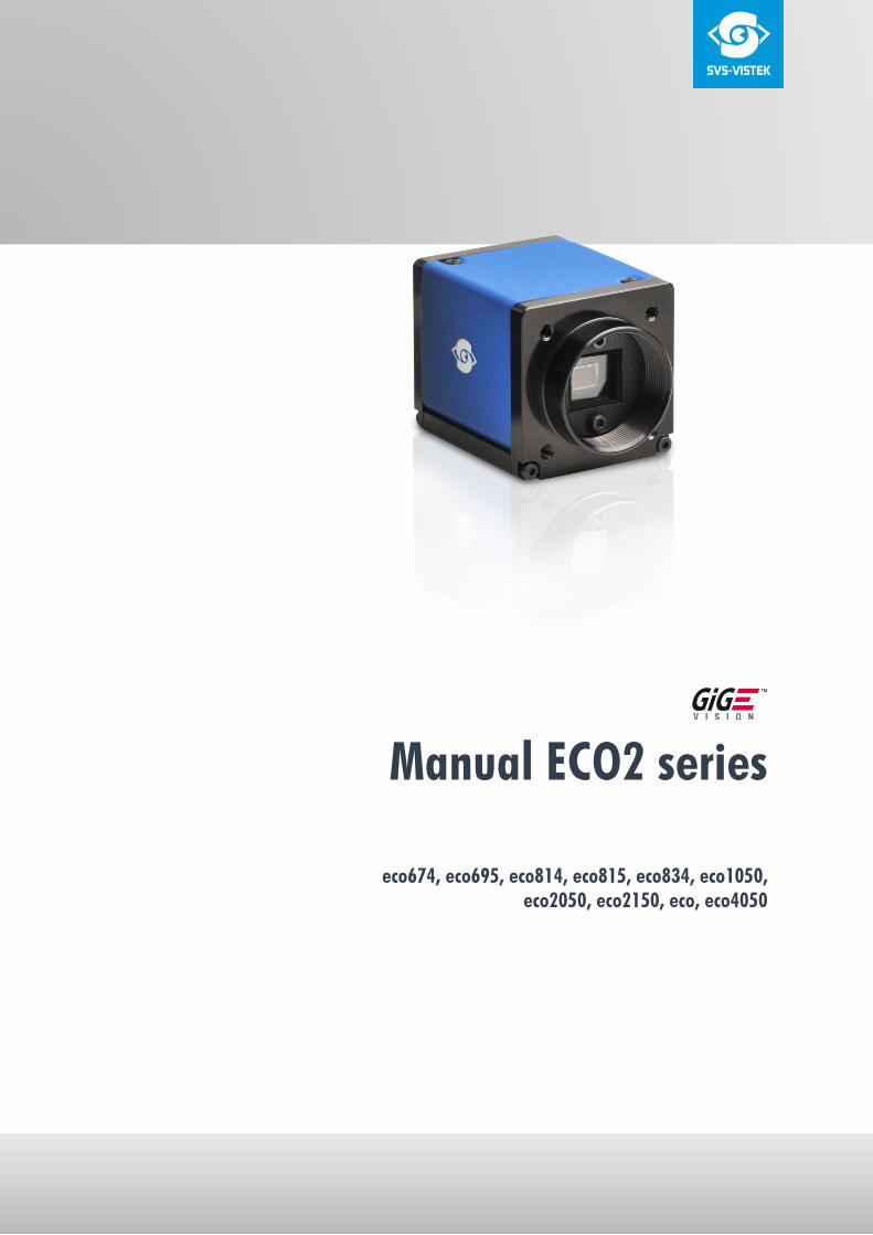
Manual ECO2 series
eco674, eco695, eco814, eco815, eco834, eco1050, eco2050, eco2150, eco, eco4050
Manual ECO 4I/O 1.24.2018
Distributor Information PYRAMID IMAGING, INC.
945 E. 11th Avenue Tampa, FL 33605
Tel.: +1 (813) 984-0125 Fax: +1 (866) 874-9521 Mail: [email protected] Web: https://pyramidimaging.com
This Operation Manual is based on the following standards:
DIN EN 62079 DIN EN ISO 12100 ISO Guide 37 DIN ISO 3864-2 DIN ISO 3864-4
This Operation Manual contains important instructions for safe and efficient handling of SVCam Cameras (hereinafter referred to as „camera“). This Operating Manual is part of the camera and must be kept accessible in the immediate vicinity of the camera for any person working on or with this camera.
Read carefully and make sure you understand this Operation Manual prior to starting any work with this camera. The basic prerequisite for safe work is compliant with all specified safety and handling instructions.
Accident prevention guidelines and general safety regulations shoud be applied.
Illustrations in this Operation Manual are provided for basic understanding and can vary from the actual model of this camera. No claims can be derived from the illustrations in this Operation Manual.
The camera in your possession has been produced with great care and has been thoroughly tested. Nonetheless, should you have reasons for complaint, then please contact Pyramid Imaging.
Copyright Protection Statement (as per DIN ISO 16016:2002-5)
Forwarding and duplicating of this document, as well as using or revealing its contents are prohibited without written approval. All rights reserved with regard to patent claims or submission of design or utility patent.
Pyramid Imaging
Contents
iii
Contents 1 Safety Messages ...................................................... 6
2 Legal Information ..................................................... 7
3 The ECO² – GigE Vision ........................................... 8
3.1 The SVCam-ECO² Series – ........................................ 8
3.2 Feature List: ............................................................ 9
3.3 GigE-Vision features ................................................. 9
3.4 4IO adds Light and Functionality .............................. 11
4 Getting Started ...................................................... 12
4.1 Contents of Camera Set .......................................... 12
4.2 Power supply ......................................................... 12
4.3 Camera status LED codes ........................................ 12
4.4 Software ............................................................... 13 4.4.1 SVCapture 2.x ............................................................ 13
4.5 Firmware .............................................................. 20 4.5.1 Firmware Update GigE ................................................ 20
4.6 GigE IP Setup ........................................................ 20
4.7 Driver Circuit Schematics ........................................ 22
5 Connectors ........................................................... 23
5.1 GigE Vision ........................................................... 23 5.1.1 Network (TCP/IP) ........................................................ 23 5.1.2 XML Files ................................................................... 26
5.2 Input / output connectors ........................................ 27
6 Dimensions ........................................................... 28
6.1 ECO² GigE C-mount ............................................. 28 6.1.1 front .......................................................................... 28 6.1.2 side Left ..................................................................... 29 6.1.3 Bottom ....................................................................... 29 6.1.4 Back .......................................................................... 30 6.1.5 Cross Section ............................................................. 30
6.2 C & CS Mount ...................................................... 31
7 Feature-Set ........................................................... 32
7.1 Basic Understanding............................................... 32 7.1.1 Basic Understanding of CCD Technology ..................... 32 7.1.2 Interline Transfer ......................................................... 33 7.1.3 Global shutter ............................................................ 34 7.1.4 Frames per Second ..................................................... 36
Contents
iv
7.1.5 Acquisition and Processing Time .................................. 36 7.1.6 Exposure .................................................................... 37 7.1.7 Auto Luminance .......................................................... 37 7.1.8 Bit-Depth ................................................................... 38 7.1.9 Color ......................................................................... 40 7.1.10 Resolution – active & effective ...................................... 41 7.1.11 Offset ........................................................................ 42 7.1.12 Gain .......................................................................... 43 7.1.13 Image Flip .................................................................. 44 7.1.14 Binning ...................................................................... 45 7.1.15 Decimation ................................................................ 46 7.1.16 Burst Mode ................................................................ 46
7.2 Camera Features ................................................... 48 7.2.1 Tap geometries ........................................................... 48 7.2.2 Standard Tap Geometries ............................................ 48 7.2.3 Tap Structure .............................................................. 48 7.2.4 Tap Reconstruction ..................................................... 50 7.2.5 Tap Balancing ............................................................ 50 7.2.6 System Clock Frequency .............................................. 51 7.2.7 Temperature Sensor .................................................... 51 7.2.8 Read-Out-Control....................................................... 51 7.2.9 Basic Capture Modes .................................................. 52 7.2.10 LookUp Table ............................................................. 55 7.2.11 ROI / AOI .................................................................. 57 7.2.12 Defect Pixel Correction ................................................ 58
7.3 I/O Features ......................................................... 58 7.3.1 Assigning I/O Lines – IOMUX ...................................... 59 7.3.2 Strobe Control ............................................................ 65 7.3.3 Sequencer .................................................................. 72 7.3.4 PWM ......................................................................... 74 7.3.5 PLC/Logical Operation on Inputs ................................. 76 7.3.6 Serial data interfaces ................................................... 77 7.3.7 Trigger-Edge Sensitivity ................................................ 80 7.3.8 Debouncing Trigger Signals ......................................... 80 7.3.9 Prescale ..................................................................... 82
7.4 IR Cut Filter ........................................................... 83
8 Specifications ........................................................ 85
8.1 eco1050*TLGEC ................................................... 85 1.1.1 Spectral Sensitivity Characteristics KAI-01050-C .............. 87 1.1.2 Spectral Sensitivity Characteristics KAI-01050-A .............. 87
8.2 eco2050*TLGEC ................................................... 88 1.1.3 Spectral Sensitivity Characteristics KAI-02050-C .............. 90 1.1.4 Spectral Sensitivity Characteristics KAI-02050-A .............. 90
8.3 eco2150*TLGEC ................................................... 91 1.1.5 Spectral Sensitivity Characteristics KAI-02150-C .............. 93 1.1.6 Spectral Sensitivity Characteristics KAI-02150-A .............. 93
1.2 eco4050*TLGEC ................................................... 94 1.2.1 Spectral Sensitivity Characteristics KAI-04050-C .............. 96 1.2.2 Spectral Sensitivity Characteristics KAI-04050-A .............. 96
8.4 eco674*TLGEC ..................................................... 97 1.2.3 Spectral Sensitivity Characteristics ICX674AQG ............... 99 1.2.4 Spectral Sensitivity Characteristics ICX674ALG ................ 99
Contents
v
8.5 eco694*TLGEC ................................................... 100 1.2.5 Spectral Sensitivity Characteristics ICX694AQG ............. 102 1.2.6 Spectral Sensitivity Characteristics ICX694ALG .............. 102
8.6 eco695*TLGEC ................................................... 103 1.2.7 Spectral Sensitivity Characteristics ICX695AQG ............. 105 1.2.8 Spectral Sensitivity Characteristics ICX695ALG .............. 105
8.7 eco814*TLGEC ................................................... 106 1.2.9 Spectral Sensitivity Characteristics ICX814AQA.............. 108 1.2.10 Spectral Sensitivity Characteristics ICX814ALA .............. 108
8.8 eco815CTLGEC .................................................. 109 1.2.11 Spectral Sensitivity Characteristics ICX815AQA.............. 111 1.2.12 Spectral Sensitivity Characteristics ICX815ALA .............. 111
8.9 eco834*TLGEC ................................................... 112 1.2.13 Spectral Sensitivity Characteristics ICX834AQG ............. 114 1.2.14 Spectral Sensitivity Characteristics ICX834ALG .............. 114
9 Terms of warranty ................................................ 115
10 Troubleshooting ................................................ 117
10.1 FAQ ............................................................... 117
10.2 Support Request Form / Check List ...................... 118
11 IP protection classes .......................................... 120
12 Glossary of Terms ............................................. 122
13 Index of figures ................................................. 125
14 Index ............................................................... 128
SVS-VISTEK– The SVCam-ECO² Series – 6
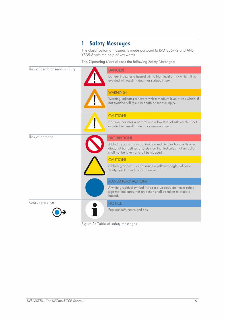
1 Safety Messages The classification of hazards is made pursuant to ISO 3864-2 and ANSI Y535.6 with the help of key words.
This Operating Manual uses the following Safety Messages:
Risk of death or serious injury
DANGER!
Danger indicates a hazard with a high level of risk which, if not avoided will result in death or serious injury.
WARNING!
Warning indicates a hazard with a medium level of risk which, if not avoided will result in death or serious injury.
CAUTION!
Caution indicates a hazard with a low level of risk which, if not avoided will result in death or serious injury.
Risk of damage
PROHIBITION!
A black graphical symbol inside a red circular band with a red diagonal bar defines a safety sign that indicates that an action shall not be taken or shall be stopped.
CAUTION!
A black graphical symbol inside a yellow triangle defines a safety sign that indicates a hazard.
MANDATORY ACTION!
A white graphical symbol inside a blue circle defines a safety sign that indicates that an action shall be taken to avoid a hazard.
Cross-reference
NOTICE
Provides references and tips
Figure 1: Table of safety messages

SVS-VISTEK–Legal Information The SVCam-ECO² Series – 7
2 Legal Information Information given within the manual accurate as to: January 29, 2018, errors and omissions excepted.
These products are designed for industrial applications only. Cameras from SVS-Vistek are not designed for life support systems where malfunction of the products might result in any risk of personal harm or injury. Customers, integrators and end users of SVS-Vistek products might sell these products and agree to do so at their own risk, as SVS-Vistek will not take any liability for any damage from improper use or sale.
Europe This camera is CE tested, rules of EN 55022:2010+AC2011 and EN61000-6-2:2005 apply.
The product is in compliance with the requirements of the following European directives:
2014/30/EU Electromagnetic compatibility (EMC) 2011/65/EU Restriction of the use of certain hazardous substances in electrical and electronic equipment (RoHS)
All SVS-VISTEK cameras comply with the recommendation of the European Union concerning RoHS Rules
USA and Canada This device complies with part 15 of the FCC Rules. Operation is subject to the following conditions: (1) This device may not cause harmful interference, and (2) this device must accept any interference received, including interference that may cause undesired operation.
Warning: This equipment is compliant with Class A of CISPR 32. In a residential environment this equipment may cause radio interference.
This equipment has been tested and found to comply with the limits for a Class A digital device, pursuant to part 15 of the FCC Rules.
It is necessary to use a shielded power supply cable. You can then use the “shield contact” on the connector which has GND contact to the camera housing. This is essential for any use. If not done and camera is destroyed due to Radio Magnetic Interference (RMI) WARRANTY is void!
• Power: US/UK and European line adapter can be delivered. Otherwise use filtered and stabilized DC power supply.
• Shock & Vibration Resistance is tested: For detailed Specifications refer to Specification.

SVS-VISTEK–The ECO² – GigE Vision The SVCam-ECO² Series – 8
3 The ECO² – GigE Vision 3.1 The SVCam-ECO² Series –
More Resolution – More Speed
The SVCam-ECO² extends the range of the SVCam-ECO: In the same housing sensors up to 12 megapixel are supported with reasonable pixel sizes and the possible bandwidth of the GigE Vision interface is fully exploited.
Compact Power
The SVCam-ECO² series expands the diversity of the SVCam-ECO series. Recent high-quality CCD sensors from ON Semiconductor and Sony are integrated and optimized in terms of image quality and operating modes. Thus, extremely demanding solutions can be solved easily.
SVS-VISTEK
The ECO² – GigE Vision 9
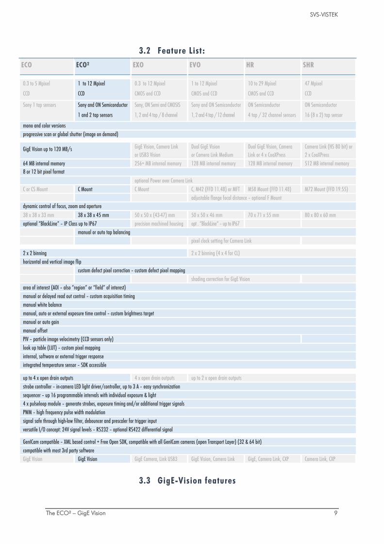
3.2 Feature List:
ECO ECO² EXO EVO HR SHR 0.3 to 5 Mpixel
CCD 1 to 12 Mpixel
CCD 0.3 to 12 Mpixel
CMOS and CCD 1 to 12 Mpixel
CMOS and CCD 10 to 29 Mpixel
CMOS and CCD 47 Mpixel
CCD Sony 1 tap sensors
Sony and ON Semiconductor
1 and 2 tap sensors Sony, ON Semi and CMOSIS
1, 2 and 4 tap / 8 channel Sony and ON Semiconductor
1, 2 and 4 tap / 12 channel ON Semiconductor
4 tap / 32 channel sensors ON Semiconductor
16 (8 x 2) tap sensor mono and color versions progressive scan or global shutter (image on demand) GigE Vision up to 120 MB/s GigE Vision, Camera Link
or USB3 Vision Dual GigE Vision or Camera Link Medium
Dual GigE Vision, Camera Link or 4 x CoaXPress
Camera Link (HS 80 bit) or 2 x CoaXPress
64 MB internal memory 256+ MB internal memory 128 MB internal memory 128 MB internal memory 512 MB internal memory 8 or 12 bit pixel format optional Power over Camera Link C or CS Mount C Mount C Mount C, M42 (FFD 11.48) or MFT M58 Mount (FFD 11.48) M72 Mount (FFD 19.55) adjustable flange focal distance – optional F Mount dynamic control of focus, zoom and aperture 38 x 38 x 33 mm 38 x 38 x 45 mm 50 x 50 x (43-47) mm 50 x 50 x 46 mm 70 x 71 x 55 mm 80 x 80 x 60 mm optional “BlackLine” – IP Class up to IP67 precision machined housing opt . “BlackLine“ – up to IP67 manual or auto tap balancing pixel clock setting for Camera Link 2 x 2 binning 2 x 2 binning (4 x 4 for CL) horizontal and vertical image flip custom defect pixel correction – custom defect pixel mapping shading correction for GigE Vision area of interest (AOI – also “region” or “field” of interest) manual or delayed read out control – custom acquisition timing
manual white balance manual, auto or external exposure time control – custom brightness target manual or auto gain manual offset PIV – particle image velocimetry (CCD sensors only) look up table (LUT) – custom pixel mapping internal, software or external trigger response integrated temperature sensor – SDK accessible up to 4 x open drain outputs 4 x open drain outputs up to 2 x open drain outputs strobe controller – in-camera LED light driver/controller, up to 3 A – easy synchronization sequencer – up 16 programmable intervals with individual exposure & light 4 x pulseloop module – generate strobes, exposure timing and/or additional trigger signals PWM – high frequency pulse width modulation signal safe through high-low filter, debouncer and prescaler for trigger input versatile I/O concept: 24V signal levels – RS232 – optional RS422 differential signal GenICam compatible – XML based control + Free Open SDK, compatible with all GenICam cameras (open Transport Layer) (32 & 64 bit) compatible with most 3rd party software GigE Vision GigE Vision GigE Camera, Link USB3 GigE Vision, Camera Link GigE, Camera Link, CXP Camera Link, CXP
3.3 GigE-Vision features
SVS-VISTEK
The ECO² – GigE Vision 10
GigE Vision is an industrial interface standard for video transmission and device control over Ethernet networks. It provides numerous software and hardware advantages for machine vision. Being an industry standard, it facilitates easy and quick interchangeability between units, shortening design cycles and reducing development costs.
> Cost effective > Wide range of „off the shelf“ industrial-standard plugs and cables > High bandwidth data transfer rate (120 MB/sec per output) > Up to 100 m range without additional switch > Wide range of applications in image processing > Remote service capability > GenICam compliant > SDK for Windows XP/10 (32/64 bit) and Linux
SVS-VISTEK
The ECO² – GigE Vision 11
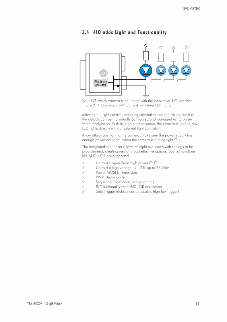
3.4 4IO adds Light and Functionality
Your SVS-Vistek camera is equipped with the innovative 4IO-interface
allowing full light control, replacing external strobe controllers. Each of the outputs can be individually configured and managed using pulse-width modulation. With its high current output, the camera is able to drive LED lights directly without external light controller.
If you attach any light to the camera, make sure the power supply has enough power not to fail when the camera is putting light ON.
The integrated sequencer allows multiple exposures with settings to be programmed, creating new and cost effective options. Logical functions like AND / OR are supported.
> Up to 4 x open drain high power OUT > Up to 4 x high voltage IN – TTL up to 25 Volts > Power MOSFET transistors > PWM strobe control > Sequencer for various configurations > PLC fuctionality with AND, OR and timers > Safe Trigger (debouncer, prescaler, high low trigger)
Figure 2: 4IO concept with up to 4 switching LED lights
SVS-VISTEK–Getting Started Contents of Camera Set 12
4 Getting Started
4.1 Contents of Camera Set > Camera > Power supply (if ordered/option) > DVD > 3D CAD files > Manuals > Software: GigE-Kit (Win 32/64 & Linux)
4.2 Power supply
Connect the power supply.
CAUTION! – This camera does not support hotplugging
1. First, connect the data cable.
2. Then connect power supply.
When using your own power supply (e.g. 10 -25 V DC) see also Hirose 12-pin for a detailed pin layout of the power connector. For power input specifications refer to specifications.
4.3 Camera status LED codes On power up, the camera will indicate its current operation status with a flashing LED on its back. The LED will change color and rhythm.
The meaning of the blinking codes translates as follows:
Figure 3: Camera status LED codes
Flashing Description
Yellow slow (1Hz) No Connection
Yellow quickly ( 8 Hz ) Assignment of Network address
Yellow permanent Network address assigned
Green permanent Connected with application
Green slow (1Hz) Streaming channel available
Green quickly ( 8 Hz) Acquisition enabled
Red slow ( 1 Hz ) Problem with initialization
Red quickly ( 8 Hz) Camera overheating
Blue permanent Waiting for trigger
Cyan permanent Exposure active
Violet permanent Readout/FVAL
SVS-VISTEK
Getting Started 13
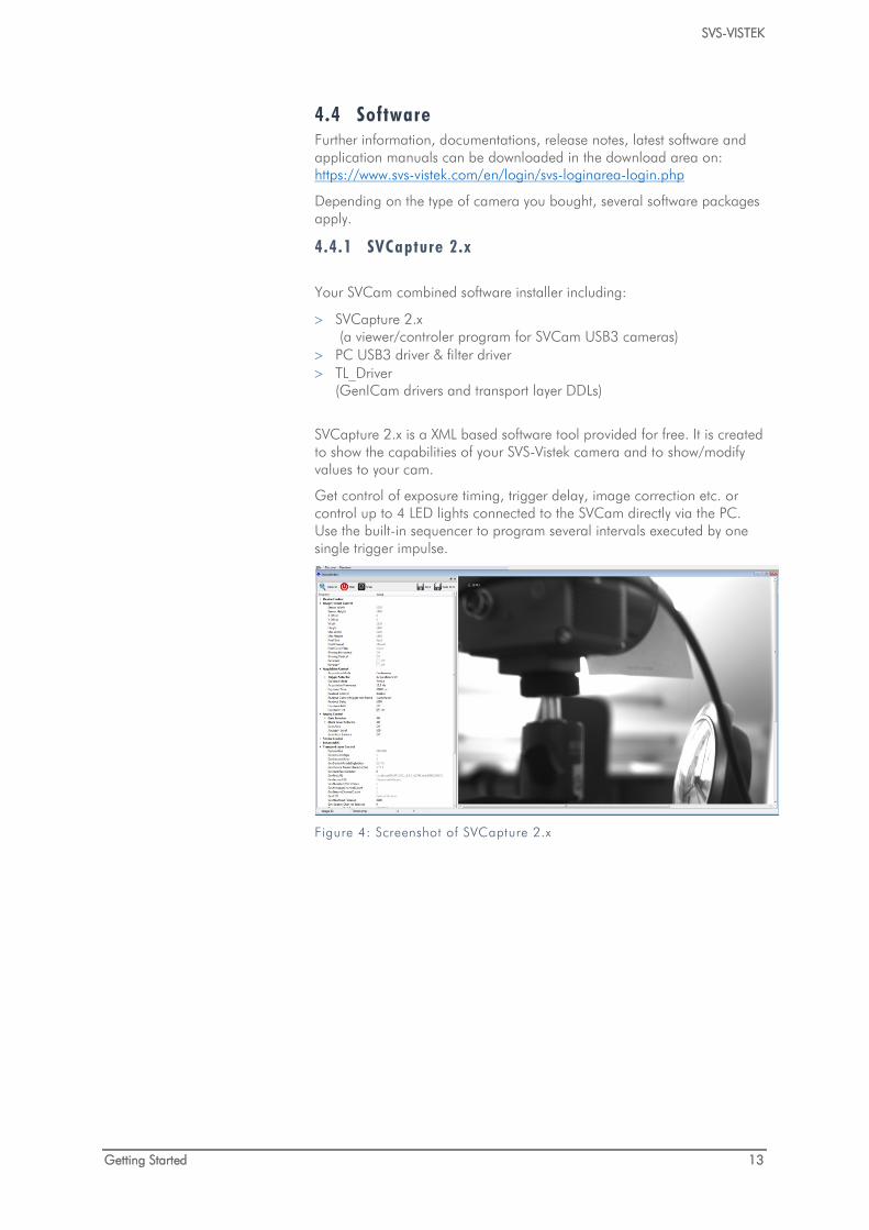
4.4 Software Further information, documentations, release notes, latest software and application manuals can be downloaded in the download area on: https://www.svs-vistek.com/en/login/svs-loginarea-login.php
Depending on the type of camera you bought, several software packages apply.
4.4.1 SVCapture 2.x
Your SVCam combined software installer including:
> SVCapture 2.x (a viewer/controler program for SVCam USB3 cameras)
> PC USB3 driver & filter driver > TL_Driver
(GenICam drivers and transport layer DDLs)
SVCapture 2.x is a XML based software tool provided for free. It is created to show the capabilities of your SVS-Vistek camera and to show/modify values to your cam.
Get control of exposure timing, trigger delay, image correction etc. or control up to 4 LED lights connected to the SVCam directly via the PC. Use the built-in sequencer to program several intervals executed by one single trigger impulse.
Figure 4: Screenshot of SVCapture 2.x
SVS-VISTEK
Getting Started 14
Software Setup Installation prosecco may differ from PC to PC. It is recommended to install the whole software package.
1. Copy/expand the installation executable file to your hard drive.
2. Run installation
3. Read and accept the terms of license agreement
4. Choose destination folder
SVS-VISTEK
Getting Started 15
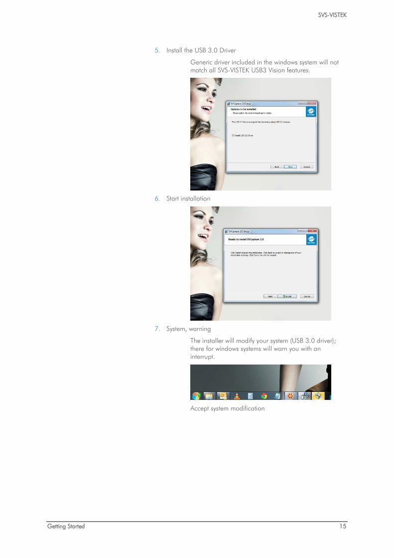
5. Install the USB 3.0 Driver
Generic driver included in the windows system will not match all SVS-VISTEK USB3 Vision features.
6. Start installation
7. System, warning
The installer will modify your system (USB 3.0 driver); there for windows systems will warn you with an interrupt.
Accept system modification
SVS-VISTEK
Getting Started 16
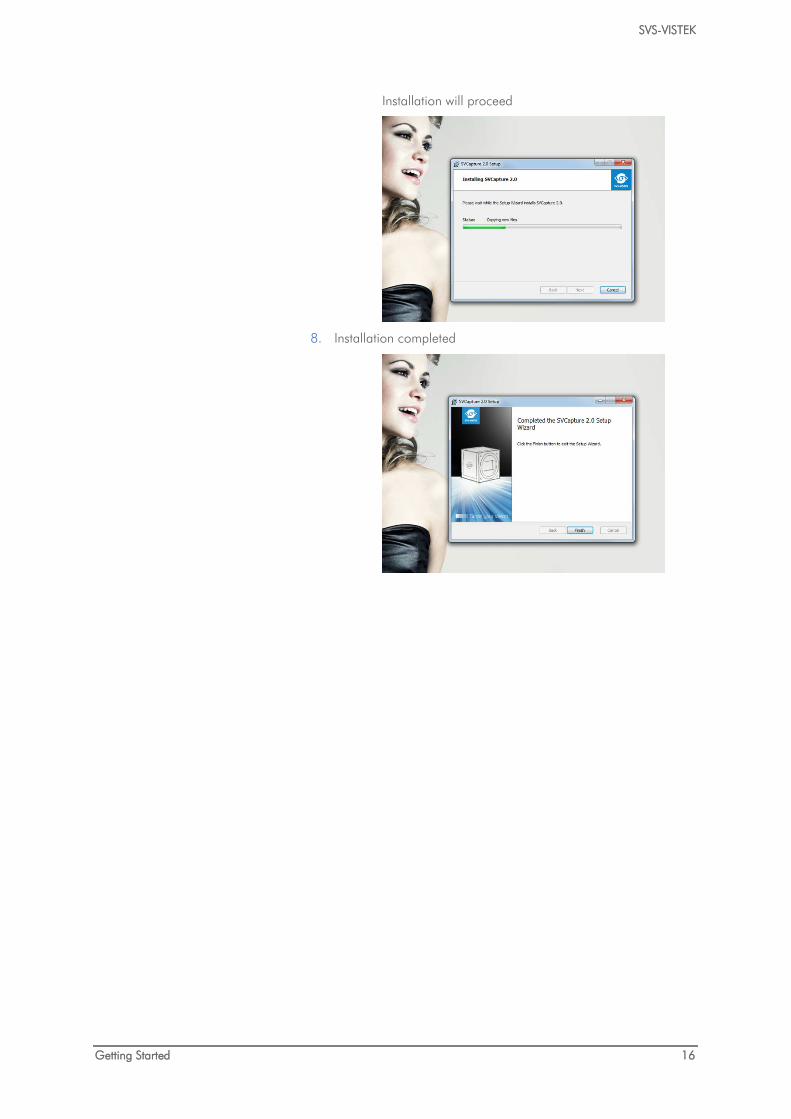
Installation will proceed
8. Installation completed
SVS-VISTEK
Getting Started 17
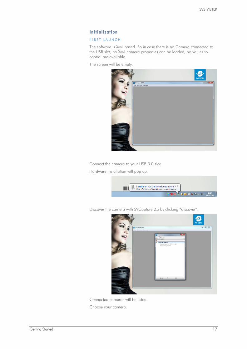
Ini t ial izat ion F I R S T L A U N C H
The software is XML based. So in case there is no Camera connected to the USB slot, no XML camera properties can be loaded, no values to control are available.
The screen will be empty.
Connect the camera to your USB 3.0 slot.
Hardware installation will pop up.
Discover the camera with SVCapture 2.x by clicking “discover”.
Connected cameras will be listed.
Choose your camera.
SVS-VISTEK
Getting Started 18
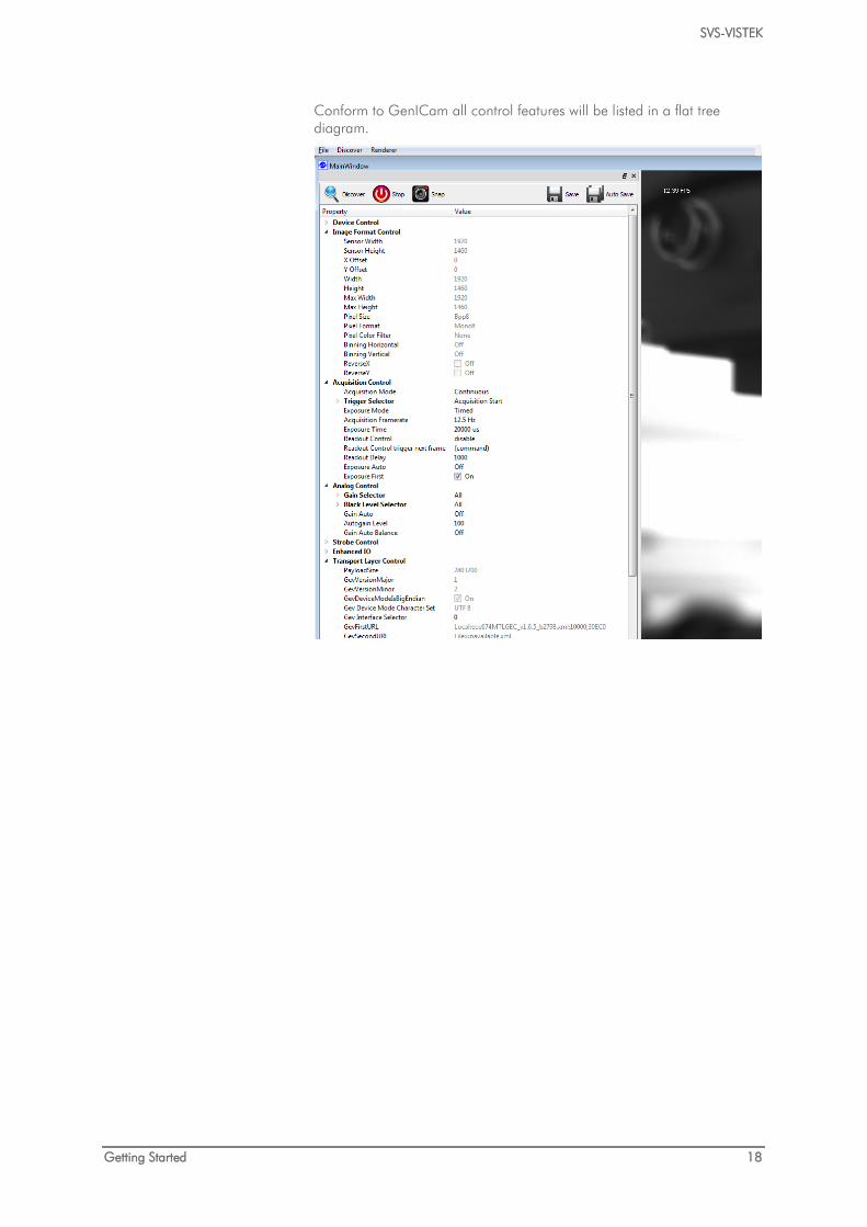
Conform to GenICam all control features will be listed in a flat tree diagram.
SVS-VISTEK
Getting Started 19
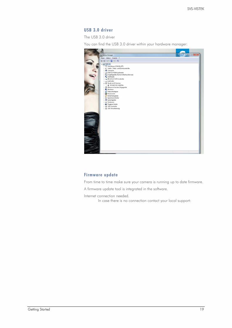
USB 3.0 driver The USB 3.0 driver
You can find the USB 3.0 driver within your hardware manager:
Firmware update From time to time make sure your camera is running up to date firmware.
A firmware update tool is integrated in the software.
Internet connection needed. In case there is no connection contact your local support:
SVS-VISTEK
Getting Started 20
4.5 Firmware Some features may not have been implemented in older versions. For updating your camera firmware to the most recent version, you need the firmware tool and a firmware file (download it from website, login area) matching your camera model.
4.5.1 Firmware Update GigE
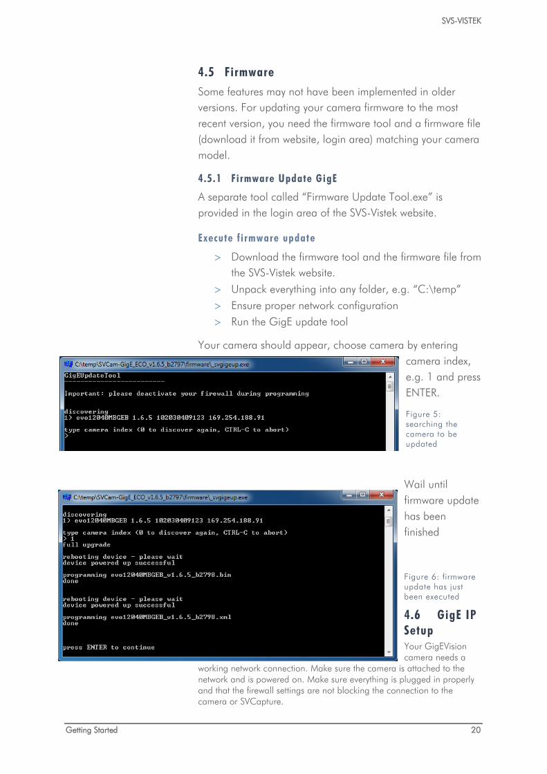
A separate tool called “Firmware Update Tool.exe” is provided in the login area of the SVS-Vistek website.
Execute f i rmware update
> Download the firmware tool and the firmware file from the SVS-Vistek website.
> Unpack everything into any folder, e.g. “C:\temp” > Ensure proper network configuration > Run the GigE update tool
Your camera should appear, choose camera by entering camera index, e.g. 1 and press ENTER.
Figure 5: searching the camera to be updated
Wail until firmware update has been finished
Figure 6: firmware update has just been executed
4.6 GigE IP Setup Your GigEVision camera needs a
working network connection. Make sure the camera is attached to the network and is powered on. Make sure everything is plugged in properly and that the firewall settings are not blocking the connection to the camera or SVCapture.
SVS-VISTEK
Getting Started 21
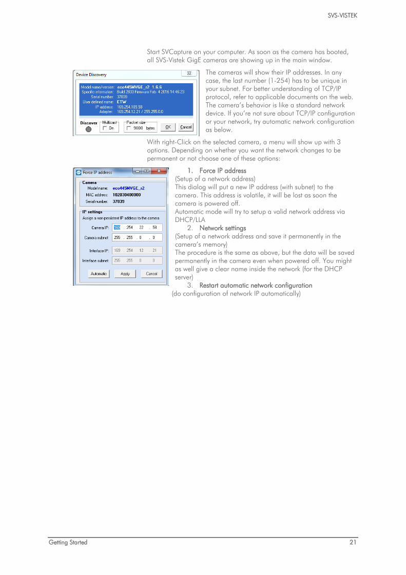
Start SVCapture on your computer. As soon as the camera has booted, all SVS-Vistek GigE cameras are showing up in the main window.
The cameras will show their IP addresses. In any case, the last number (1-254) has to be unique in your subnet. For better understanding of TCP/IP protocol, refer to applicable documents on the web. The camera’s behavior is like a standard network device. If you’re not sure about TCP/IP configuration or your network, try automatic network configuration as below.
With right-Click on the selected camera, a menu will show up with 3 options. Depending on whether you want the network changes to be permanent or not choose one of these options:
1. Force IP address (Setup of a network address) This dialog will put a new IP address (with subnet) to the camera. This address is volatile, it will be lost as soon the camera is powered off. Automatic mode will try to setup a valid network address via DHCP/LLA
2. Network settings (Setup of a network address and save it permanently in the camera’s memory) The procedure is the same as above, but the data will be saved permanently in the camera even when powered off. You might as well give a clear name inside the network (for the DHCP server)
3. Restart automatic network configuration (do configuration of network IP automatically)
SVS-VISTEK
Getting Started 22
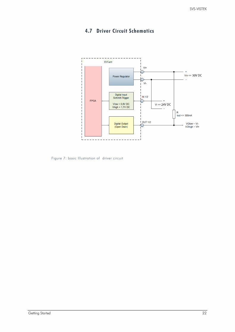
4.7 Driver Circuit Schematics
Figure 7: basic Illustration of driver circuit
SVS-VISTEK–Connectors GigE Vision 23
5 Connectors
5.1 GigE Vision
5.1.1 Network (TCP/IP)
Address Assignment
By default, the camera does not have a persistent IP address.
When forcing an IP address by using the PC internal network dialog, changes are only valid until the next restart of the Camera.
For a peer-to-peer connection of a GigE camera to a PC a network address assignment based on LLA (Local Link Address) is recommended. This involves a network mask “255.255.0.0” as well as a fixed preamble “169.254.xxx.xxx” of the network address range. A GigE camera will fall back to LLA when no DHCP server is available and no fixed network address was assigned to the camera.
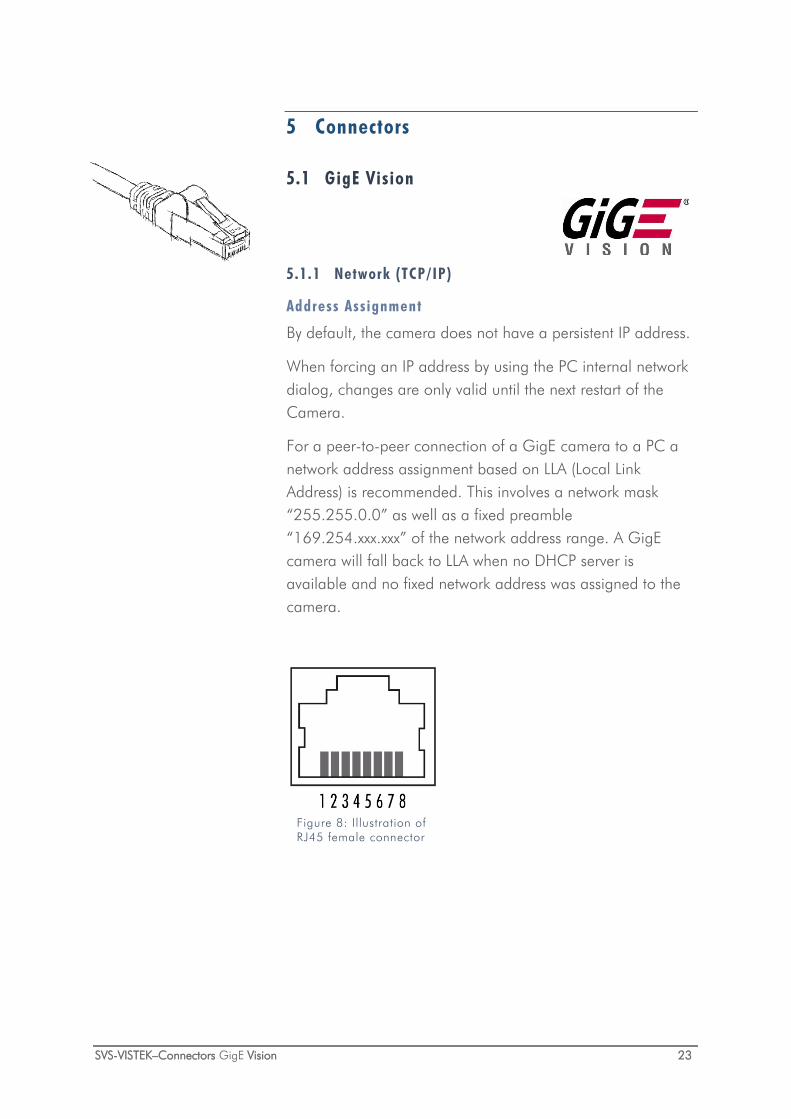
Figure 8: Illustration of RJ45 female connector
SVS-VISTEK
Connectors 24
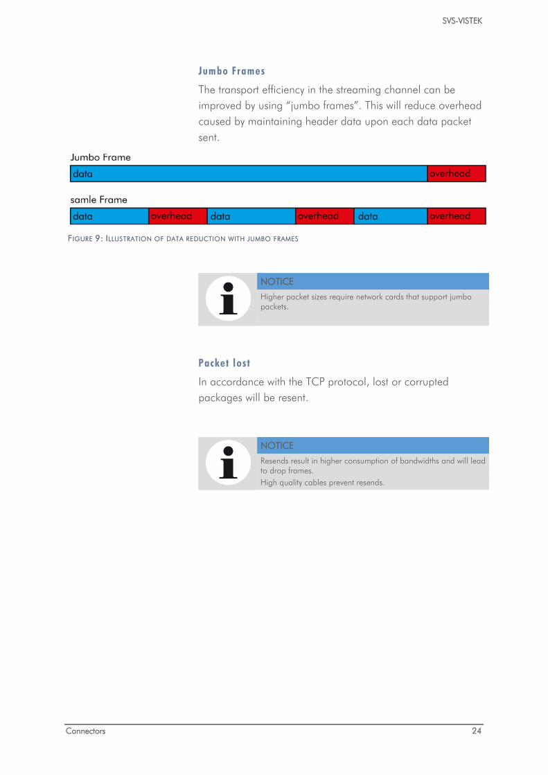
Jumbo Frames
The transport efficiency in the streaming channel can be improved by using “jumbo frames”. This will reduce overhead caused by maintaining header data upon each data packet sent.
FIGURE 9: ILLUSTRATION OF DATA REDUCTION WITH JUMBO FRAMES
NOTICE
Higher packet sizes require network cards that support jumbo packets.
Packet lost
In accordance with the TCP protocol, lost or corrupted packages will be resent.
NOTICE
Resends result in higher consumption of bandwidths and will lead to drop frames. High quality cables prevent resends.
SVS-VISTEK
Connectors 25
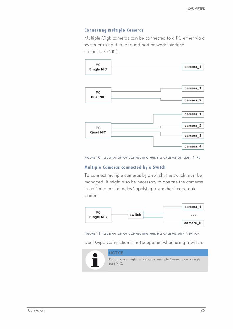
Connecting mult iple Cameras
Multiple GigE cameras can be connected to a PC either via a switch or using dual or quad port network interface connectors (NIC).
FIGURE 10: ILLUSTRATION OF CONNECTING MULTIPLE CAMERAS ON MULTI NIPS
Multiple Cameras connected by a Switch
To connect multiple cameras by a switch, the switch must be managed. It might also be necessary to operate the cameras in an “inter packet delay” applying a smother image data stream.
FIGURE 11: ILLUSTRATION OF CONNECTING MULTIPLE CAMERAS WITH A SWITCH
Dual GigE Connection is not supported when using a switch.
NOTICE
Performance might be lost using multiple Cameras on a single port NIC.
SVS-VISTEK
Connectors 26
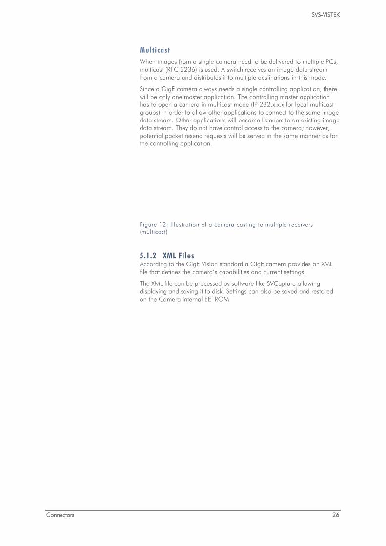
Multicast When images from a single camera need to be delivered to multiple PCs, multicast (RFC 2236) is used. A switch receives an image data stream from a camera and distributes it to multiple destinations in this mode.
Since a GigE camera always needs a single controlling application, there will be only one master application. The controlling master application has to open a camera in multicast mode (IP 232.x.x.x for local multicast groups) in order to allow other applications to connect to the same image data stream. Other applications will become listeners to an existing image data stream. They do not have control access to the camera; however, potential packet resend requests will be served in the same manner as for the controlling application.
Figure 12: Illustration of a camera casting to multiple receivers (multicast)
5.1.2 XML Fi les According to the GigE Vision standard a GigE camera provides an XML file that defines the camera’s capabilities and current settings.
The XML file can be processed by software like SVCapture allowing displaying and saving it to disk. Settings can also be saved and restored on the Camera internal EEPROM.
SVS-VISTEK
Connectors 27
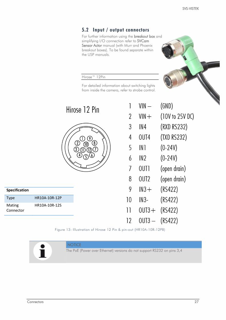
5.2 Input / output connectors For further information using the breakout box and simplifying I/O connection refer to SVCam Sensor Actor manual (with Murr and Phoenix breakout boxes). To be found separate within the USP manuals.
Hirose™ 12Pin
For detailed information about switching lights from inside the camera, refer to strobe control.
Figure 13: Illustration of Hirose 12 Pin & pin-out (HR10A-10R-12PB)
NOTICE
The PoE (Power over Ethernet) versions do not support RS232 on pins 3,4
Specification
Type HR10A-10R-12P
Mating Connector
HR10A-10R-12S

SVS-VISTEK–Dimensions ECO² GigE C-mount 28
6 Dimensions All length units in mm. Find drawings in the web download area at https://www.svs-vistek.com/en/support/svs-support-download-center.php
CAD step files available with valid login at SVS-VISTEK.com
6.1 ECO² GigE C-mount CAD step files available on DVD or SVS-VISTEK.com.
Including: eco1050CTLGEC, eco1050MTLGEC, eco2050CTLGEC, eco2050MTLGEC, eco2150CTLGEC, eco2150MTLGEC, eco4050CTLGEC, eco4050MTLGEC, eco674CTLGEC, eco674MTLGEC, eco694CTLGEC, eco694MTLGEC, eco695CTLGEC, eco695MTLGEC, eco814CTLGEC, eco814MTLGEC, eco815CTLGEC, eco815MTLGEC, eco834CTLGEC, eco834MTLGEC
6.1.1 front
SVS-VISTEK
Dimensions 29
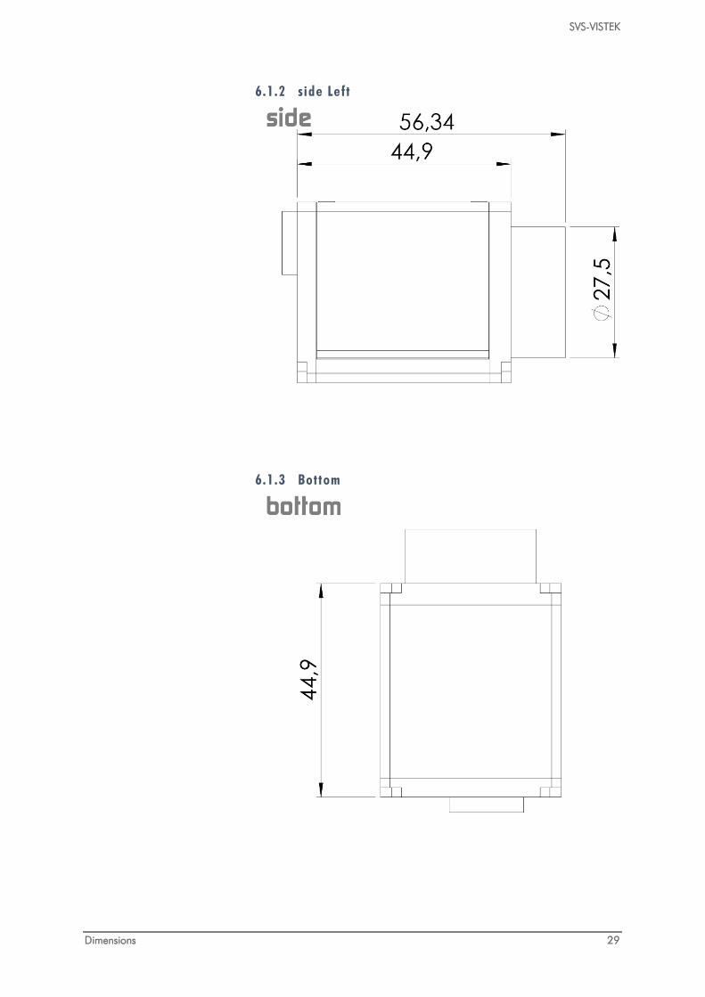
6.1.2 side Left
6.1.3 Bottom
SVS-VISTEK
Dimensions 30
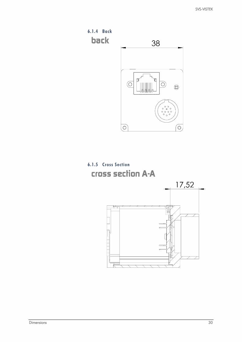
6.1.4 Back
6.1.5 Cross Sect ion
SVS-VISTEK
Dimensions 31
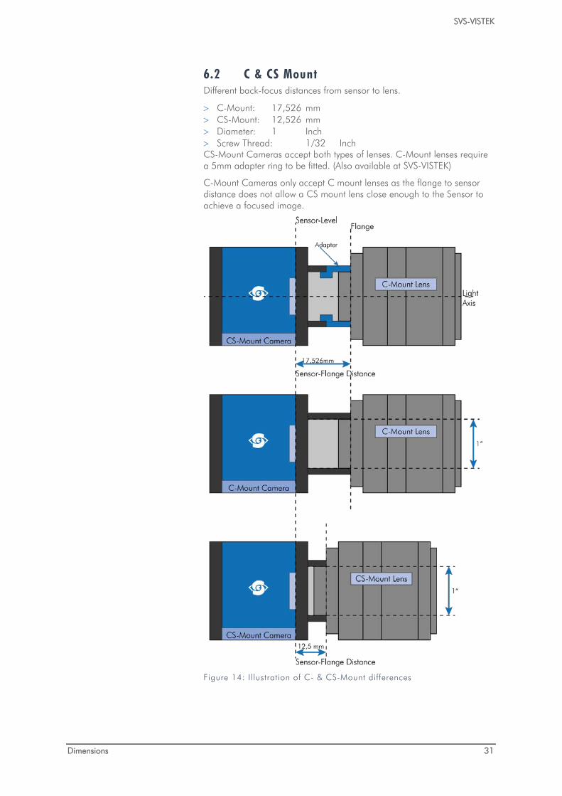
6.2 C & CS Mount Different back-focus distances from sensor to lens.
> C-Mount: 17,526 mm > CS-Mount: 12,526 mm > Diameter: 1 Inch > Screw Thread: 1/32 Inch CS-Mount Cameras accept both types of lenses. C-Mount lenses require a 5mm adapter ring to be fitted. (Also available at SVS-VISTEK)
C-Mount Cameras only accept C mount lenses as the flange to sensor distance does not allow a CS mount lens close enough to the Sensor to achieve a focused image.
Figure 14: Illustration of C- & CS-Mount differences
SVS-VISTEK–Feature-Set Basic Understanding 32
7 Feature-Set 7.1 Basic Understanding
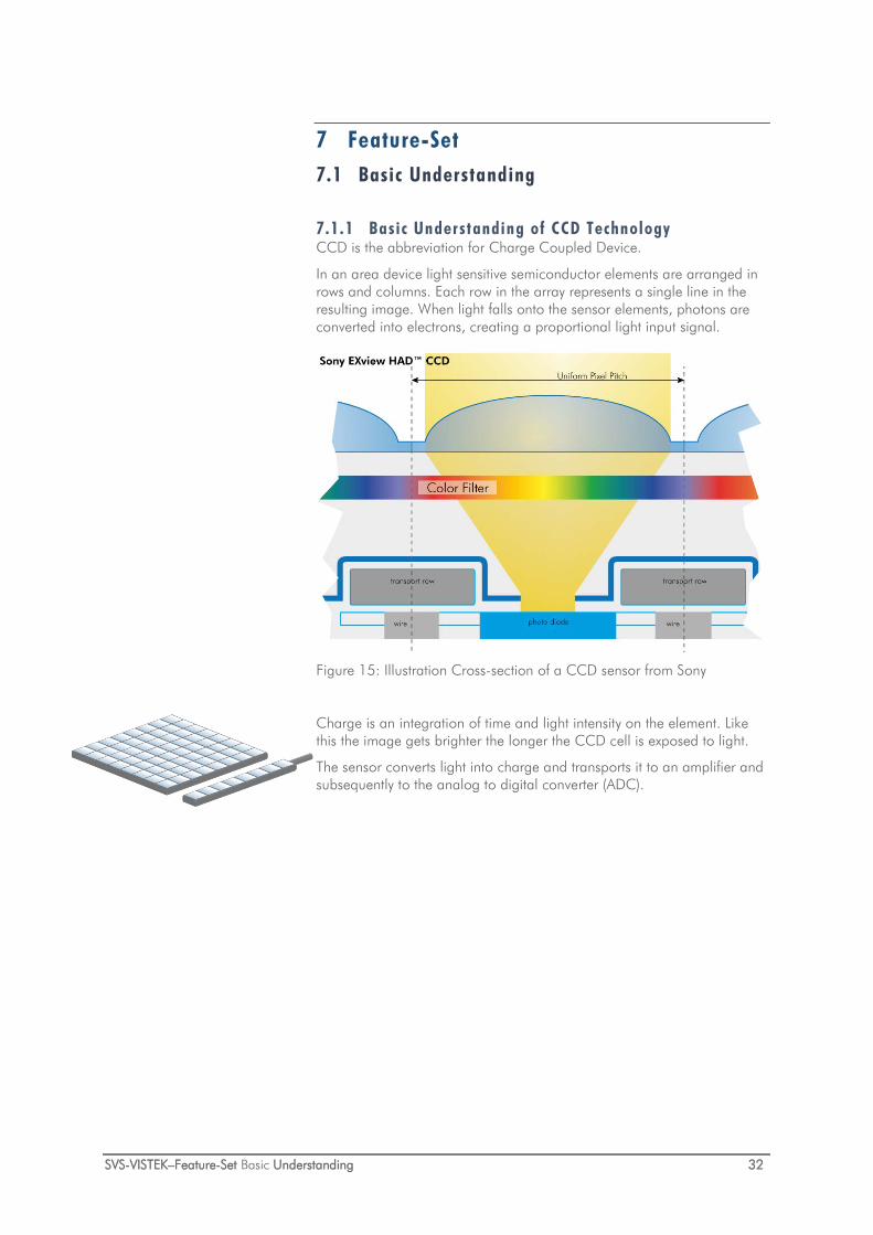
7.1.1 Basic Understanding of CCD Technology CCD is the abbreviation for Charge Coupled Device.
In an area device light sensitive semiconductor elements are arranged in rows and columns. Each row in the array represents a single line in the resulting image. When light falls onto the sensor elements, photons are converted into electrons, creating a proportional light input signal.
Figure 15: Illustration Cross-section of a CCD sensor from Sony
Charge is an integration of time and light intensity on the element. Like this the image gets brighter the longer the CCD cell is exposed to light.
The sensor converts light into charge and transports it to an amplifier and subsequently to the analog to digital converter (ADC).
SVS-VISTEK
Feature-Set 33
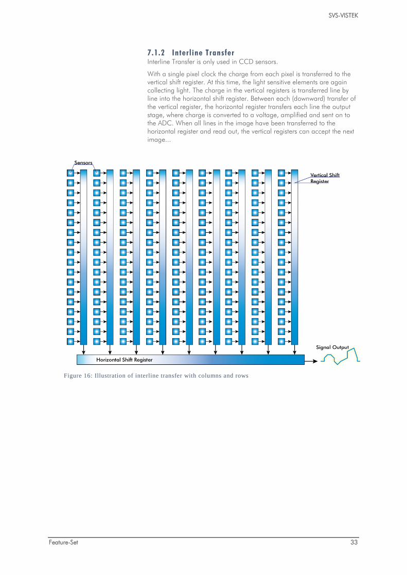
7.1.2 Interl ine Transfer Interline Transfer is only used in CCD sensors.
With a single pixel clock the charge from each pixel is transferred to the vertical shift register. At this time, the light sensitive elements are again collecting light. The charge in the vertical registers is transferred line by line into the horizontal shift register. Between each (downward) transfer of the vertical register, the horizontal register transfers each line the output stage, where charge is converted to a voltage, amplified and sent on to the ADC. When all lines in the image have been transferred to the horizontal register and read out, the vertical registers can accept the next image...
Figure 16: Illustration of interline transfer with columns and rows
SVS-VISTEK
Feature-Set 34
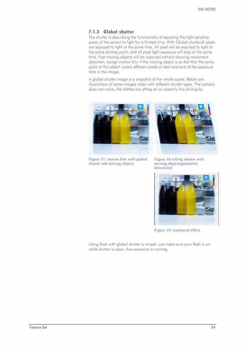
7.1.3 Global shutter The shutter is describing the functionality of exposing the light sensitive pixels of the sensor to light for a limited time. With Global shutterall pixels are exposed to light at the same time. All pixel will be exposed to light at the same starting point, and all pixel light exposure will stop at the same time. Fast moving objects will be captured without showing movement distortion, except motion blur if the moving object is so fast that the same point of the object covers different pixels at start and end of the exposure time in the image.
A global shutter image is a snapshot of the whole scene. Below are illustrations of some images taken with different shutter types. The camera does not move, the bottles are sitting on an assemly line driving by.
Figure 17: motion blur with global shutter and moving objects
Figure 18 rolling shutter with moving objects(geometric distortion)
Figure 19: interlaced effect
Using flash with global shutter is simpel: just make sure your flash is on while shutter is open, thus exposure is running.
SVS-VISTEK
Feature-Set 35
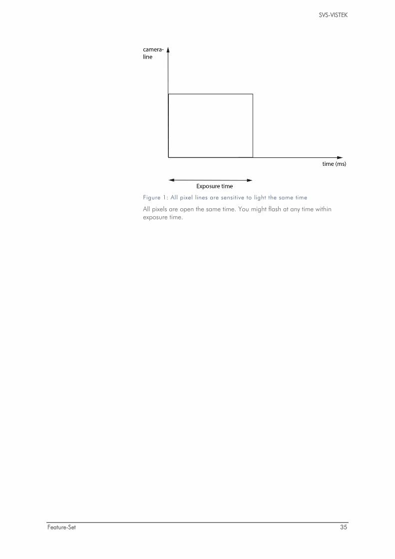
Figure 1: All pixel lines are sensitive to light the same time
All pixels are open the same time. You might flash at any time within exposure time.
SVS-VISTEK
Feature-Set 36
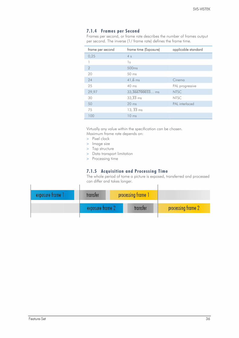
7.1.4 Frames per Second Frames per second, or frame rate describes the number of frames output per second. The inverse (1/ frame rate) defines the frame time.
frame per second frame time (Exposure) applicable standard
0,25 4 s
1 1s
2 500ms
20 50 ms
24 41,6 ms Cinema
25 40 ms PAL progressive
29,97 33,366700033… ms NTSC
30 33,33 ms NTSC
50 20 ms PAL interlaced
75 13, 33 ms
100 10 ms
Virtually any value within the specification can be chosen. Maximum frame rate depends on: > Pixel clock > Image size > Tap structure > Data transport limitation > Processing time
7.1.5 Acquisi t ion and Processing Time The whole period of tome a picture is exposed, transferred and processed can differ and takes longer.
SVS-VISTEK
Feature-Set 37
7.1.6 Exposure See various exposure and timing modes in chapter: Basic capture modes.
Combine various exposure timings with PWM LED illumination, refer to sequencer.
Sett ing Exposure t ime Exposure time can be set by width of the external or internal triggers or programmed by a given value.
7.1.7 Auto Luminance
Auto Luminance automatically calculates and adjusts exposure time and gain, frame-by-frame.
The auto exposure or automatic luminance control of the camera signal is a combination of an automatic adjustment of the camera exposure time (electronic shutter) and the gain.
The first priority is to adjust the exposure time and if the exposure time range is not sufficient, gain adjustment is applied. It is possibility to pre-define the range (min. / max. -values) of exposure time and of gain.
The condition to use this function is to set a targeted averaged brightness of the camera image. The algorithm computes a gain and exposure for each image to reach this target brightness in the next image (control loop). Enabling this functionality uses always both – gain and exposure time.
Limitation As this feature is based on a control loop, the result is only useful in an averaged, continuous stream of images. Strong variations in brightness from one image to next image will result in a swing of the control loop. Therefore it is not recommended to use the auto-luminance function in such cases.
SVS-VISTEK
Feature-Set 38
Figure 21: Simplified illustration of a quantification graph
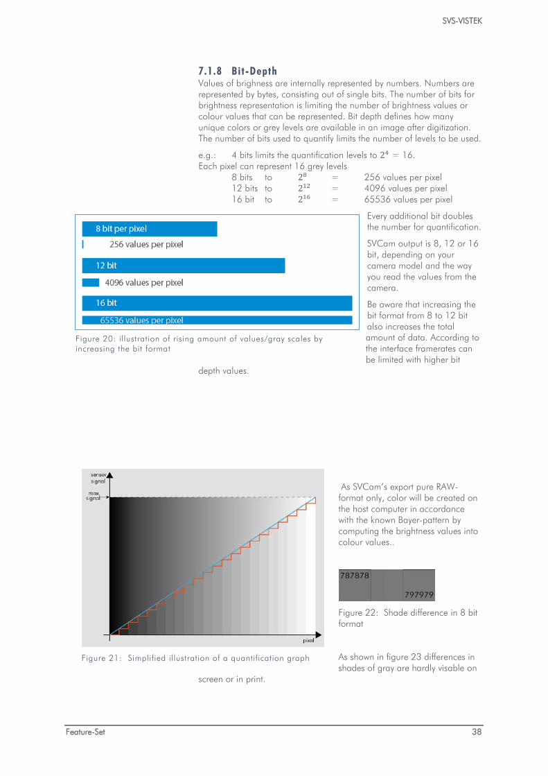
7.1.8 Bit-Depth Values of brighness are internally represented by numbers. Numbers are represented by bytes, consisting out of single bits. The number of bits for brightness representation is limiting the number of brightness values or colour values that can be represented. Bit depth defines how many unique colors or grey levels are available in an image after digitization. The number of bits used to quantify limits the number of levels to be used.
e.g.: 4 bits limits the quantification levels to 24 = 16. Each pixel can represent 16 grey levels 8 bits to 28 = 256 values per pixel 12 bits to 212 = 4096 values per pixel 16 bit to 216 = 65536 values per pixel
Every additional bit doubles the number for quantification.
SVCam output is 8, 12 or 16 bit, depending on your camera model and the way you read the values from the camera.
Be aware that increasing the bit format from 8 to 12 bit also increases the total amount of data. According to the interface framerates can be limited with higher bit
depth values.
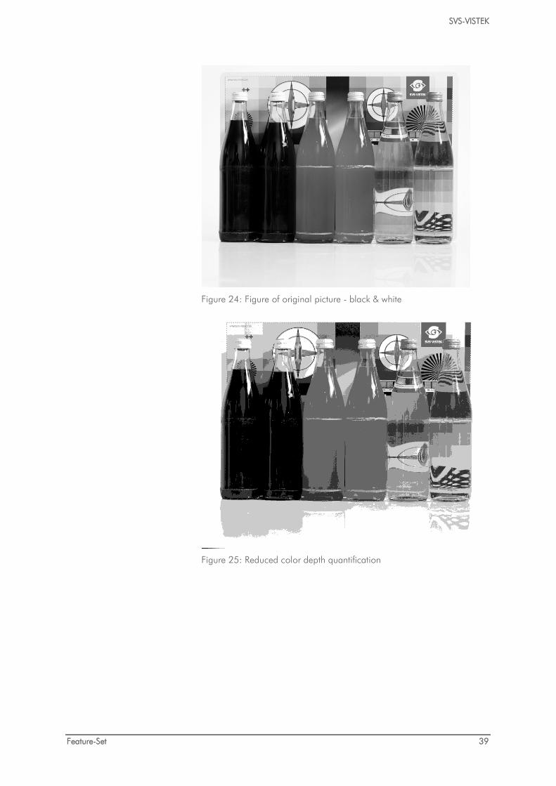
As SVCam’s export pure RAW-format only, color will be created on the host computer in accordance with the known Bayer-pattern by computing the brightness values into colour values..
Figure 22: Shade difference in 8 bit format
As shown in figure 23 differences in shades of gray are hardly visable on
screen or in print.
Figure 20: illustration of rising amount of values/gray scales by increasing the bit format
SVS-VISTEK
Feature-Set 39
Figure 24: Figure of original picture - black & white
Figure 25: Reduced color depth quantification
SVS-VISTEK
Feature-Set 40
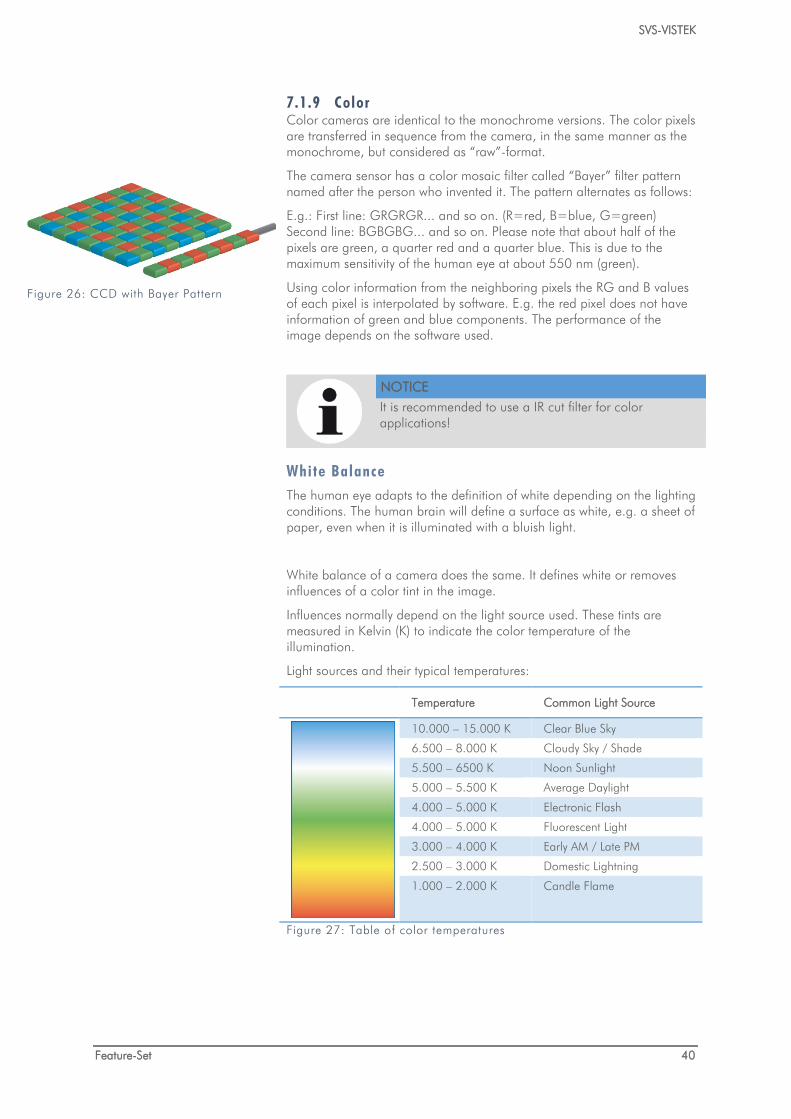
7.1.9 Color Color cameras are identical to the monochrome versions. The color pixels are transferred in sequence from the camera, in the same manner as the monochrome, but considered as “raw”-format.
The camera sensor has a color mosaic filter called “Bayer” filter pattern named after the person who invented it. The pattern alternates as follows:
E.g.: First line: GRGRGR... and so on. (R=red, B=blue, G=green) Second line: BGBGBG... and so on. Please note that about half of the pixels are green, a quarter red and a quarter blue. This is due to the maximum sensitivity of the human eye at about 550 nm (green).
Using color information from the neighboring pixels the RG and B values of each pixel is interpolated by software. E.g. the red pixel does not have information of green and blue components. The performance of the image depends on the software used.
NOTICE
It is recommended to use a IR cut filter for color applications!
White Balance The human eye adapts to the definition of white depending on the lighting conditions. The human brain will define a surface as white, e.g. a sheet of paper, even when it is illuminated with a bluish light.
White balance of a camera does the same. It defines white or removes influences of a color tint in the image.
Influences normally depend on the light source used. These tints are measured in Kelvin (K) to indicate the color temperature of the illumination.
Light sources and their typical temperatures:
Temperature Common Light Source
10.000 – 15.000 K Clear Blue Sky
6.500 – 8.000 K Cloudy Sky / Shade
5.500 – 6500 K Noon Sunlight
5.000 – 5.500 K Average Daylight
4.000 – 5.000 K Electronic Flash
4.000 – 5.000 K Fluorescent Light
3.000 – 4.000 K Early AM / Late PM
2.500 – 3.000 K Domestic Lightning
1.000 – 2.000 K Candle Flame
Figure 27: Table of color temperatures
Figure 26: CCD with Bayer Pattern
SVS-VISTEK
Feature-Set 41
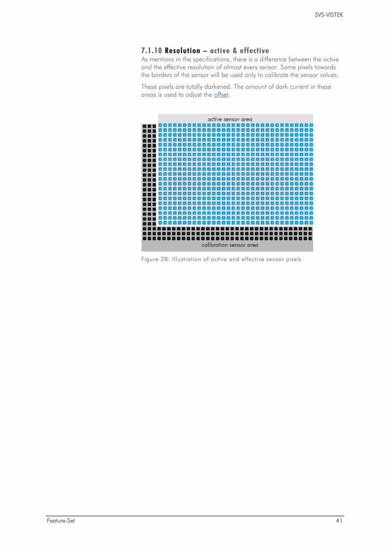
7.1.10 Resolution – act ive & effect ive As mentions in the specifications, there is a difference between the active and the effective resolution of almost every sensor. Some pixels towards the borders of the sensor will be used only to calibrate the sensor values.
These pixels are totally darkened. The amount of dark current in these areas is used to adjust the offset.
Figure 28: Illustration of active and effective sensor pixels
SVS-VISTEK
Feature-Set 42
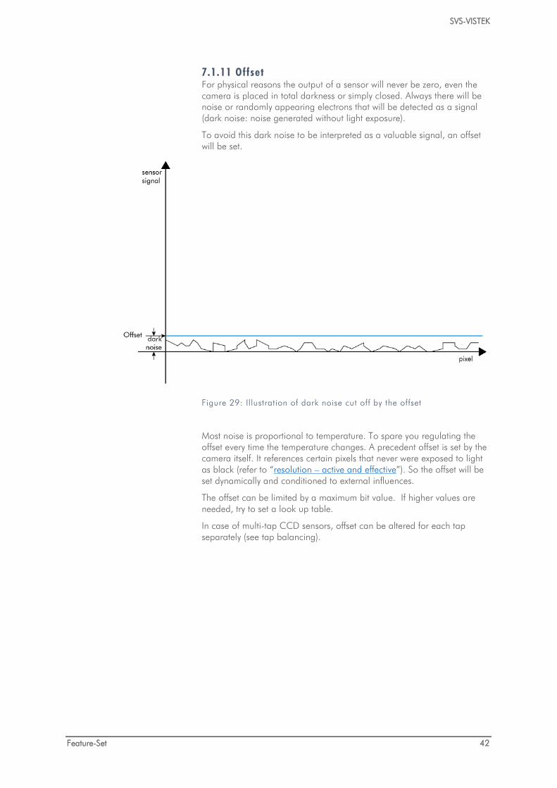
7.1.11 Offset For physical reasons the output of a sensor will never be zero, even the camera is placed in total darkness or simply closed. Always there will be noise or randomly appearing electrons that will be detected as a signal (dark noise: noise generated without light exposure).
To avoid this dark noise to be interpreted as a valuable signal, an offset will be set.
Figure 29: Illustration of dark noise cut off by the offset
Most noise is proportional to temperature. To spare you regulating the offset every time the temperature changes. A precedent offset is set by the camera itself. It references certain pixels that never were exposed to light as black (refer to “resolution – active and effective”). So the offset will be set dynamically and conditioned to external influences.
The offset can be limited by a maximum bit value. If higher values are needed, try to set a look up table.
In case of multi-tap CCD sensors, offset can be altered for each tap separately (see tap balancing).
SVS-VISTEK
Feature-Set 43
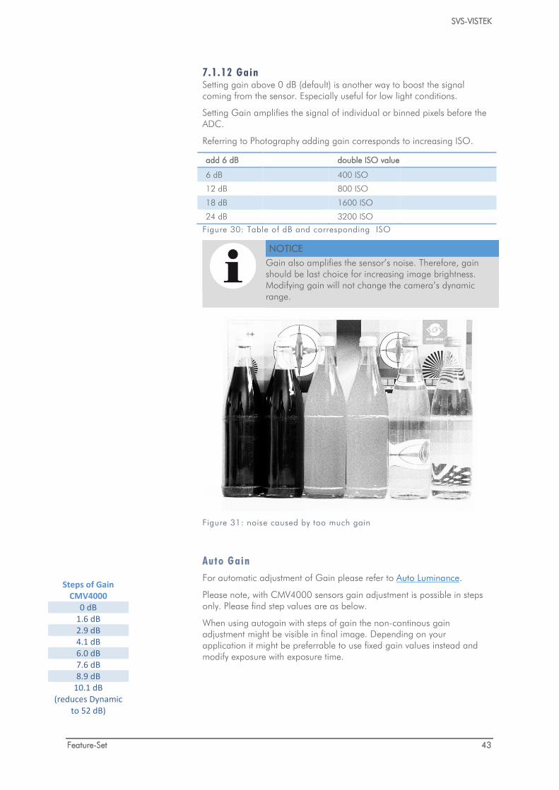
7.1.12 Gain Setting gain above 0 dB (default) is another way to boost the signal coming from the sensor. Especially useful for low light conditions.
Setting Gain amplifies the signal of individual or binned pixels before the ADC.
Referring to Photography adding gain corresponds to increasing ISO.
add 6 dB double ISO value
6 dB 400 ISO
12 dB 800 ISO
18 dB 1600 ISO
24 dB 3200 ISO
Figure 30: Table of dB and corresponding ISO
NOTICE
Gain also amplifies the sensor’s noise. Therefore, gain should be last choice for increasing image brightness. Modifying gain will not change the camera’s dynamic range.
Figure 31: noise caused by too much gain
Auto Gain For automatic adjustment of Gain please refer to Auto Luminance.
Please note, with CMV4000 sensors gain adjustment is possible in steps only. Please find step values are as below.
When using autogain with steps of gain the non-continous gain adjustment might be visible in final image. Depending on your application it might be preferrable to use fixed gain values instead and modify exposure with exposure time.
Steps of Gain CMV4000
0 dB 1.6 dB 2.9 dB 4.1 dB 6.0 dB 7.6 dB 8.9 dB
10.1 dB (reduces Dynamic
to 52 dB)
SVS-VISTEK
Feature-Set 44
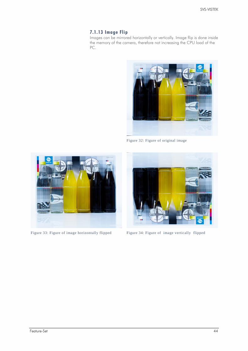
7.1.13 Image Fl ip Images can be mirrored horizontally or vertically. Image flip is done inside the memory of the camera, therefore not increasing the CPU load of the PC.
Figure 32: Figure of original image
Figure 33: Figure of image horizontally flipped Figure 34: Figure of image vertically flipped
SVS-VISTEK
Feature-Set 45
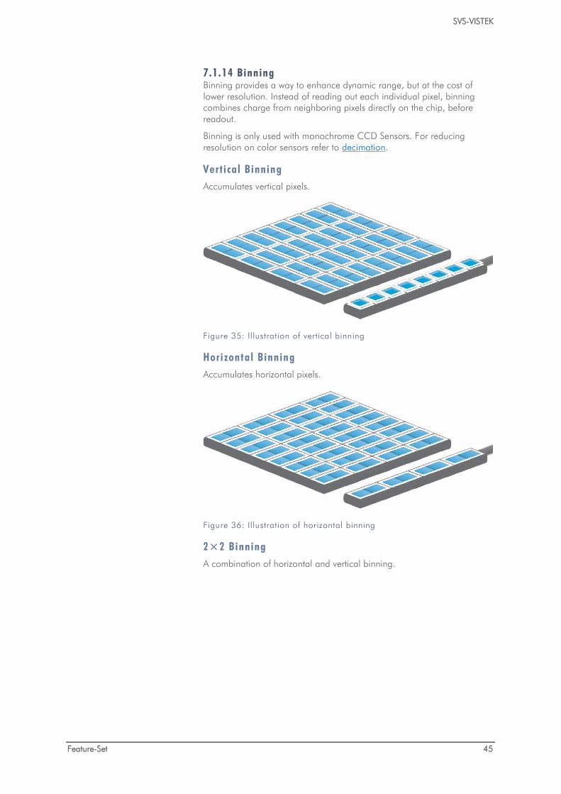
7.1.14 Binning Binning provides a way to enhance dynamic range, but at the cost of lower resolution. Instead of reading out each individual pixel, binning combines charge from neighboring pixels directly on the chip, before readout.
Binning is only used with monochrome CCD Sensors. For reducing resolution on color sensors refer to decimation.
Vert ical Binning Accumulates vertical pixels.
Figure 35: Illustration of vertical binning
Horizontal Binning Accumulates horizontal pixels.
Figure 36: Illustration of horizontal binning
2×2 Binning A combination of horizontal and vertical binning.
SVS-VISTEK
Feature-Set 46
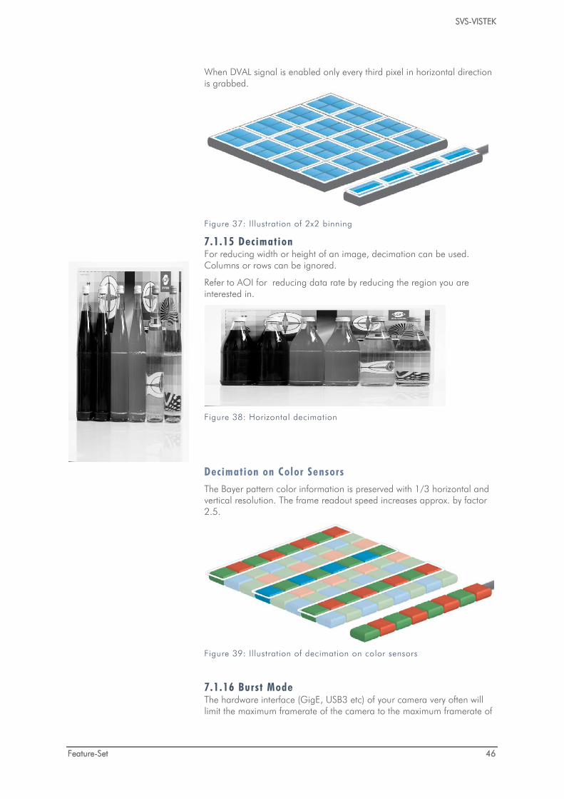
When DVAL signal is enabled only every third pixel in horizontal direction is grabbed.
Figure 37: Illustration of 2x2 binning
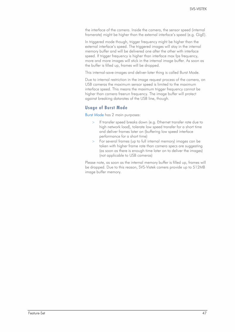
7.1.15 Decimation For reducing width or height of an image, decimation can be used. Columns or rows can be ignored.
Refer to AOI for reducing data rate by reducing the region you are interested in.
Figure 38: Horizontal decimation
Decimation on Color Sensors The Bayer pattern color information is preserved with 1/3 horizontal and vertical resolution. The frame readout speed increases approx. by factor 2.5.
Figure 39: Illustration of decimation on color sensors
7.1.16 Burst Mode The hardware interface (GigE, USB3 etc) of your camera very often will limit the maximum framerate of the camera to the maximum framerate of
SVS-VISTEK
Feature-Set 47
the interface of the camera. Inside the camera, the sensor speed (internal framerate) might be higher than the external interface’s speed (e.g. GigE).
In triggered mode though, trigger frequency might be higher than the external interface’s speed. The triggered images will stay in the internal memory buffer and will be delivered one after the other with interface speed. If trigger frequency is higher than interface max fps frequency, more and more images will stick in the internal image buffer. As soon as the buffer is filled up, frames will be dropped.
This internal-save-images and deliver-later thing is called Burst Mode.
Due to internal restriction in the image request process of the camera, on USB cameras the maximum sensor speed is limited to the maximum interface speed. This means the maximum trigger frequency cannot be higher than camera freerun frequency. The image buffer will protect against breaking datarates of the USB line, though.
Usage of Burst Mode Burst Mode has 2 main purposes:
> If transfer speed breaks down (e.g. Ethernet transfer rate due to high network load), tolerate low speed transfer for a short time and deliver frames later on (buffering low speed interface performance for a short time)
> For several frames (up to full internal memory) images can be taken with higher frame rate than camera specs are suggesting (as soon as there is enough time later on to deliver the images) (not applicable to USB cameras)
Please note, as soon as the internal memory buffer is filled up, frames will be dropped. Due to this reason, SVS-Vistek camers provide up to 512MB image buffer memory.
SVS-VISTEK
Feature-Set 48
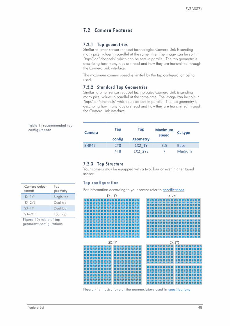
Camera output format
Tap geometry
1X–1Y Single tap
1X–2YE Dual tap
2X–1Y Dual tap
2X–2YE Four tap
Figure 40: table of tap geometry/configurations
7.2 Camera Features
7.2.1 Tap geometries Similar to other sensor readout technologies Camera Link is sending many pixel values in parallel at the same time. The image can be split in “taps” or “channels” which can be sent in parallel. The tap geometry is describing how many taps are read and how they are transmitted through the Camera Link interface.
The maximum camera speed is limited by the tap configuration being used.
7.2.2 Standard Tap Geometries Similar to other sensor readout technologies Camera Link is sending many pixel values in parallel at the same time. The image can be split in “taps” or “channels” which can be sent in parallel. The tap geometry is describing how many taps are read and how they are transmitted through the Camera Link interface.
Camera Tap Tap Maximum
speed CL type config geometry
SHR47 2T8 1X2_1Y 3,5 Base
4T8 1X2_2YE 7 Medium
7.2.3 Tap Structure Your camera may be equipped with a two, four or even higher taped sensor.
Tap configuration For information according to your sensor refer to specifications.
Figure 41: Illustrations of the nomenclature used in specifications
Table 1: recommended tap configurations
SVS-VISTEK
Feature-Set 49
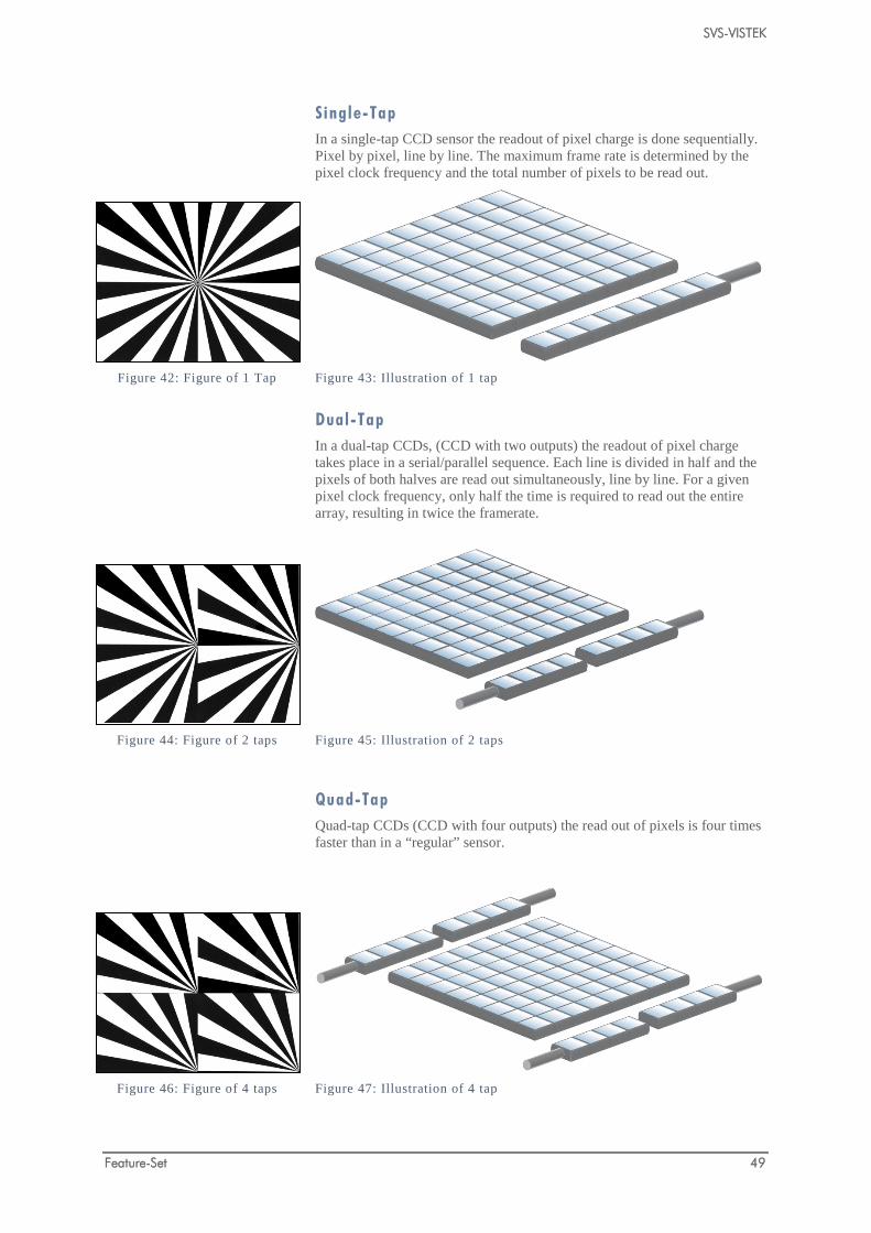
Single-Tap
Figure 42: Figure of 1 Tap
In a single-tap CCD sensor the readout of pixel charge is done sequentially. Pixel by pixel, line by line. The maximum frame rate is determined by the pixel clock frequency and the total number of pixels to be read out.
Figure 43: Illustration of 1 tap
Dual-Tap
Figure 44: Figure of 2 taps
In a dual-tap CCDs, (CCD with two outputs) the readout of pixel charge takes place in a serial/parallel sequence. Each line is divided in half and the pixels of both halves are read out simultaneously, line by line. For a given pixel clock frequency, only half the time is required to read out the entire array, resulting in twice the framerate.
Figure 45: Illustration of 2 taps
Quad-Tap
Figure 46: Figure of 4 taps
Quad-tap CCDs (CCD with four outputs) the read out of pixels is four times faster than in a “regular” sensor.
Figure 47: Illustration of 4 tap
SVS-VISTEK
Feature-Set 50
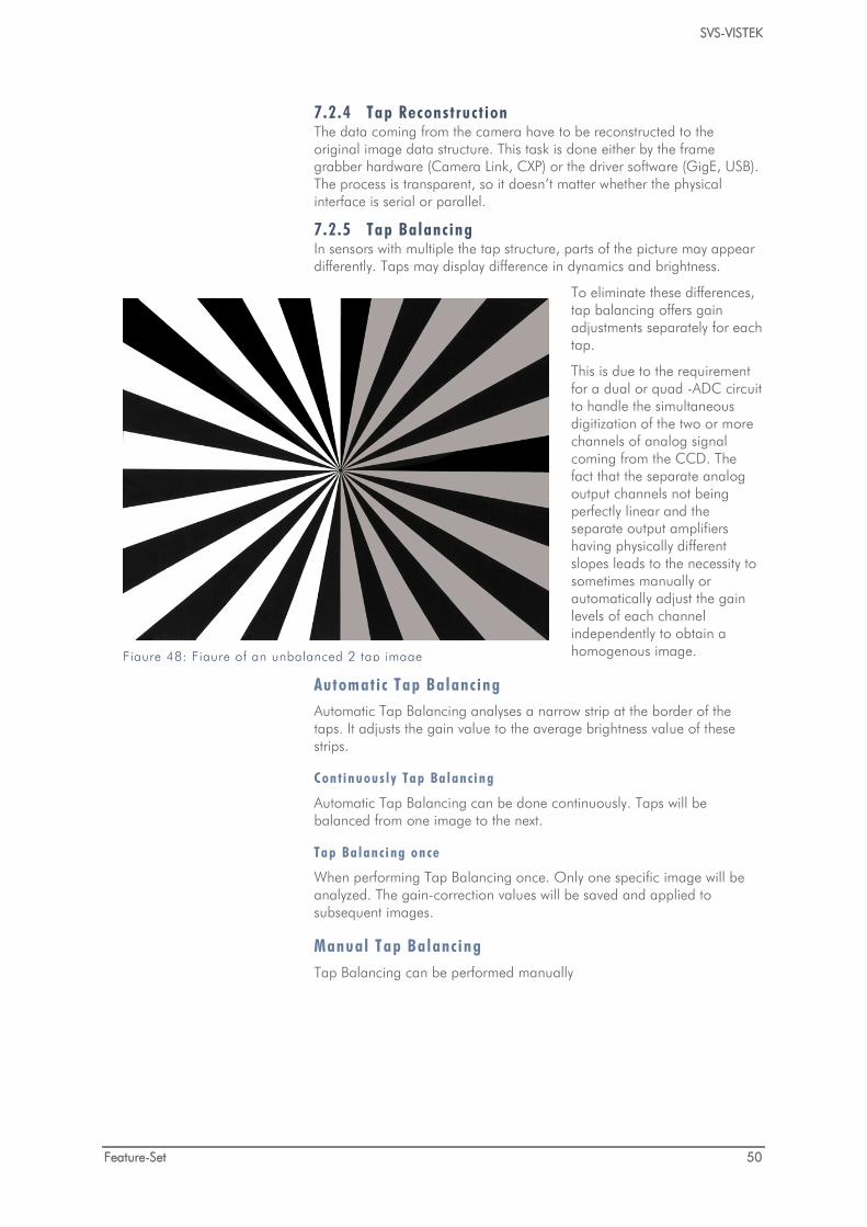
Figure 48: Figure of an unbalanced 2 tap image
7.2.4 Tap Reconstruct ion The data coming from the camera have to be reconstructed to the original image data structure. This task is done either by the frame grabber hardware (Camera Link, CXP) or the driver software (GigE, USB). The process is transparent, so it doesn’t matter whether the physical interface is serial or parallel.
7.2.5 Tap Balancing In sensors with multiple the tap structure, parts of the picture may appear differently. Taps may display difference in dynamics and brightness.
To eliminate these differences, tap balancing offers gain adjustments separately for each tap.
This is due to the requirement for a dual or quad -ADC circuit to handle the simultaneous digitization of the two or more channels of analog signal coming from the CCD. The fact that the separate analog output channels not being perfectly linear and the separate output amplifiers having physically different slopes leads to the necessity to sometimes manually or automatically adjust the gain levels of each channel independently to obtain a homogenous image.
Automatic Tap Balancing Automatic Tap Balancing analyses a narrow strip at the border of the taps. It adjusts the gain value to the average brightness value of these strips.
Con t inuous ly Tap Ba lanc i ng
Automatic Tap Balancing can be done continuously. Taps will be balanced from one image to the next.
Tap Ba lanc i ng once
When performing Tap Balancing once. Only one specific image will be analyzed. The gain-correction values will be saved and applied to subsequent images.
Manual Tap Balancing Tap Balancing can be performed manually
SVS-VISTEK
Feature-Set 51
7.2.6 System Clock Frequency Default system clock frequency in almost every SVCam is set to 66.6 MHz. To validate your system frequency refer to: specifications.
Using the system clock as reference of time, time settings can only be made in steps. In this example, the transfer rate is 66.7 MHz, thus resulting in steps of 15 ns.
𝑡 =1
66. 6 𝑀𝑀𝑀=
1
66 666 666. 6 1𝑠
= 15 ∙ 10−9 𝑠 = 15 𝑛𝑠
NOTICE
Use multiples of 15 ns to write durations into camera memory
7.2.7 Temperature Sensor A temperature sensor is installed on the mainboard of the camera.
To avoid overheating, the temperature is constantly monitored and read. Besides software monitoring, the camera indicates high temperature by a red flashing LED. (See flashing LED codes)
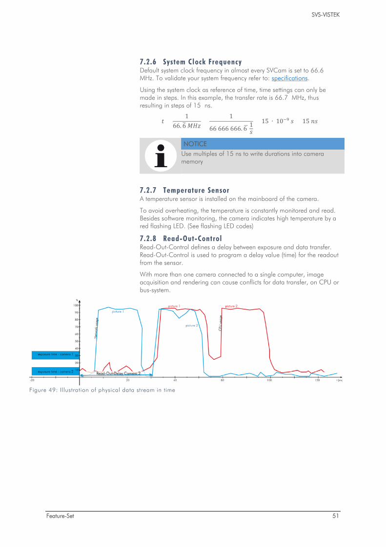
7.2.8 Read-Out-Control Read-Out-Control defines a delay between exposure and data transfer. Read-Out-Control is used to program a delay value (time) for the readout from the sensor.
With more than one camera connected to a single computer, image acquisition and rendering can cause conflicts for data transfer, on CPU or bus-system.
Figure 49: Illustration of physical data stream in time
SVS-VISTEK
Feature-Set 52
7.2.9 Basic Capture Modes
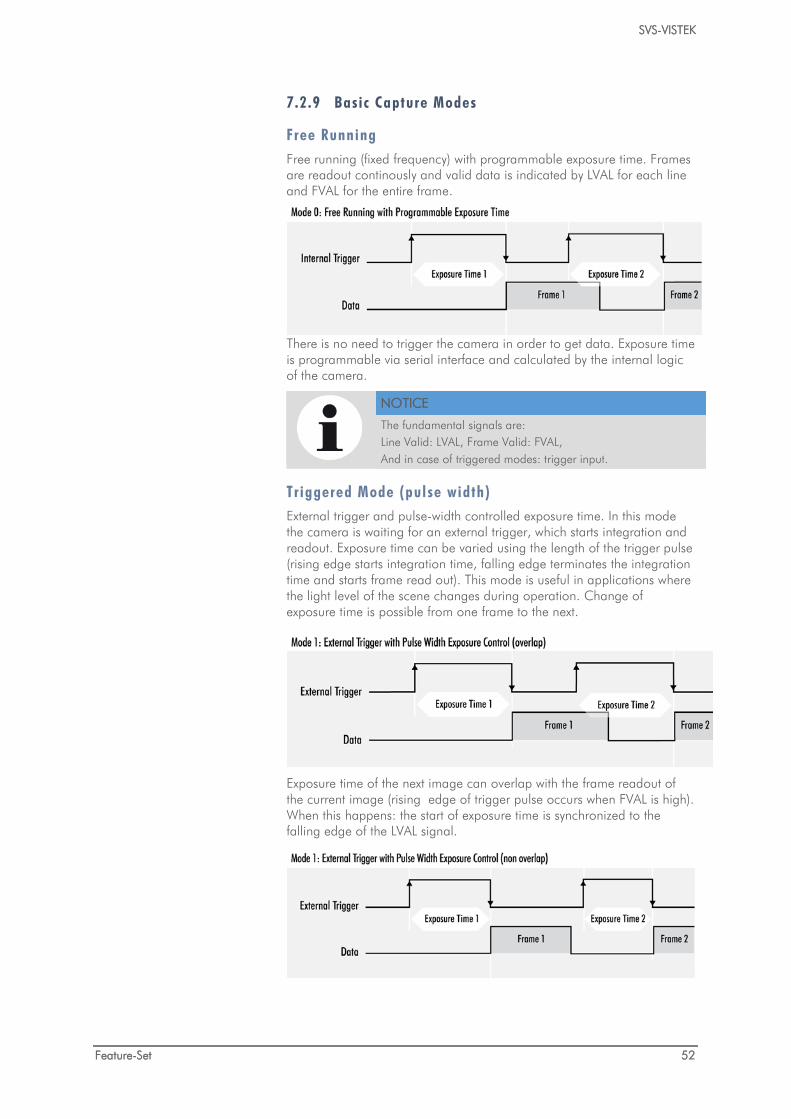
Free Running Free running (fixed frequency) with programmable exposure time. Frames are readout continously and valid data is indicated by LVAL for each line and FVAL for the entire frame.
There is no need to trigger the camera in order to get data. Exposure time is programmable via serial interface and calculated by the internal logic of the camera.
NOTICE
The fundamental signals are: Line Valid: LVAL, Frame Valid: FVAL, And in case of triggered modes: trigger input.
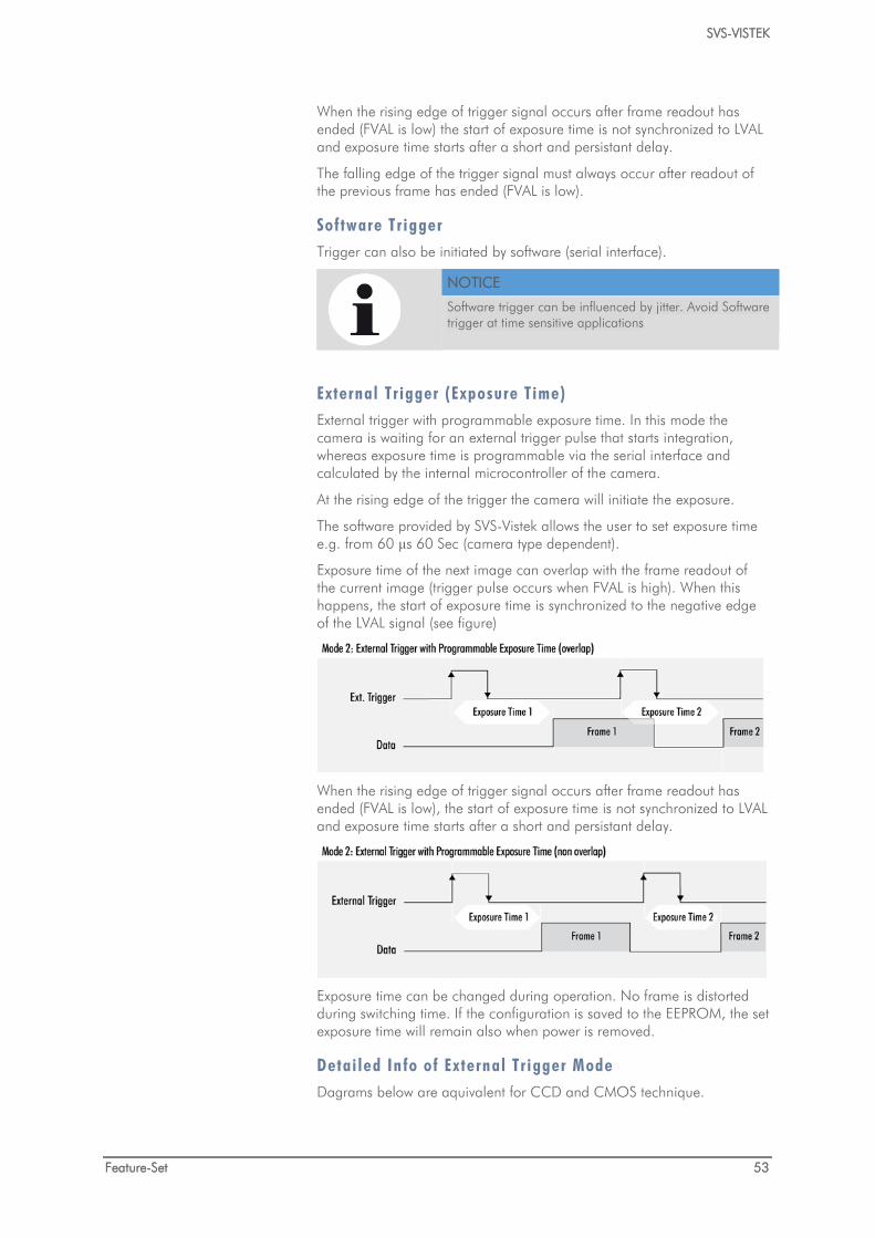
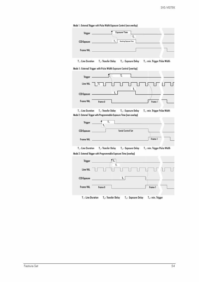
Triggered Mode (pulse width) External trigger and pulse-width controlled exposure time. In this mode the camera is waiting for an external trigger, which starts integration and readout. Exposure time can be varied using the length of the trigger pulse (rising edge starts integration time, falling edge terminates the integration time and starts frame read out). This mode is useful in applications where the light level of the scene changes during operation. Change of exposure time is possible from one frame to the next.
Exposure time of the next image can overlap with the frame readout of the current image (rising edge of trigger pulse occurs when FVAL is high). When this happens: the start of exposure time is synchronized to the falling edge of the LVAL signal.
SVS-VISTEK
Feature-Set 53
When the rising edge of trigger signal occurs after frame readout has ended (FVAL is low) the start of exposure time is not synchronized to LVAL and exposure time starts after a short and persistant delay.
The falling edge of the trigger signal must always occur after readout of the previous frame has ended (FVAL is low).
Software Trigger Trigger can also be initiated by software (serial interface).
NOTICE
Software trigger can be influenced by jitter. Avoid Software trigger at time sensitive applications
External Tr igger (Exposure Time) External trigger with programmable exposure time. In this mode the camera is waiting for an external trigger pulse that starts integration, whereas exposure time is programmable via the serial interface and calculated by the internal microcontroller of the camera.
At the rising edge of the trigger the camera will initiate the exposure.
The software provided by SVS-Vistek allows the user to set exposure time e.g. from 60 μs 60 Sec (camera type dependent).
Exposure time of the next image can overlap with the frame readout of the current image (trigger pulse occurs when FVAL is high). When this happens, the start of exposure time is synchronized to the negative edge of the LVAL signal (see figure)
When the rising edge of trigger signal occurs after frame readout has ended (FVAL is low), the start of exposure time is not synchronized to LVAL and exposure time starts after a short and persistant delay.
Exposure time can be changed during operation. No frame is distorted during switching time. If the configuration is saved to the EEPROM, the set exposure time will remain also when power is removed.
Detai led Info of External Tr igger Mode Dagrams below are aquivalent for CCD and CMOS technique.
SVS-VISTEK
Feature-Set 54
SVS-VISTEK
Feature-Set 55
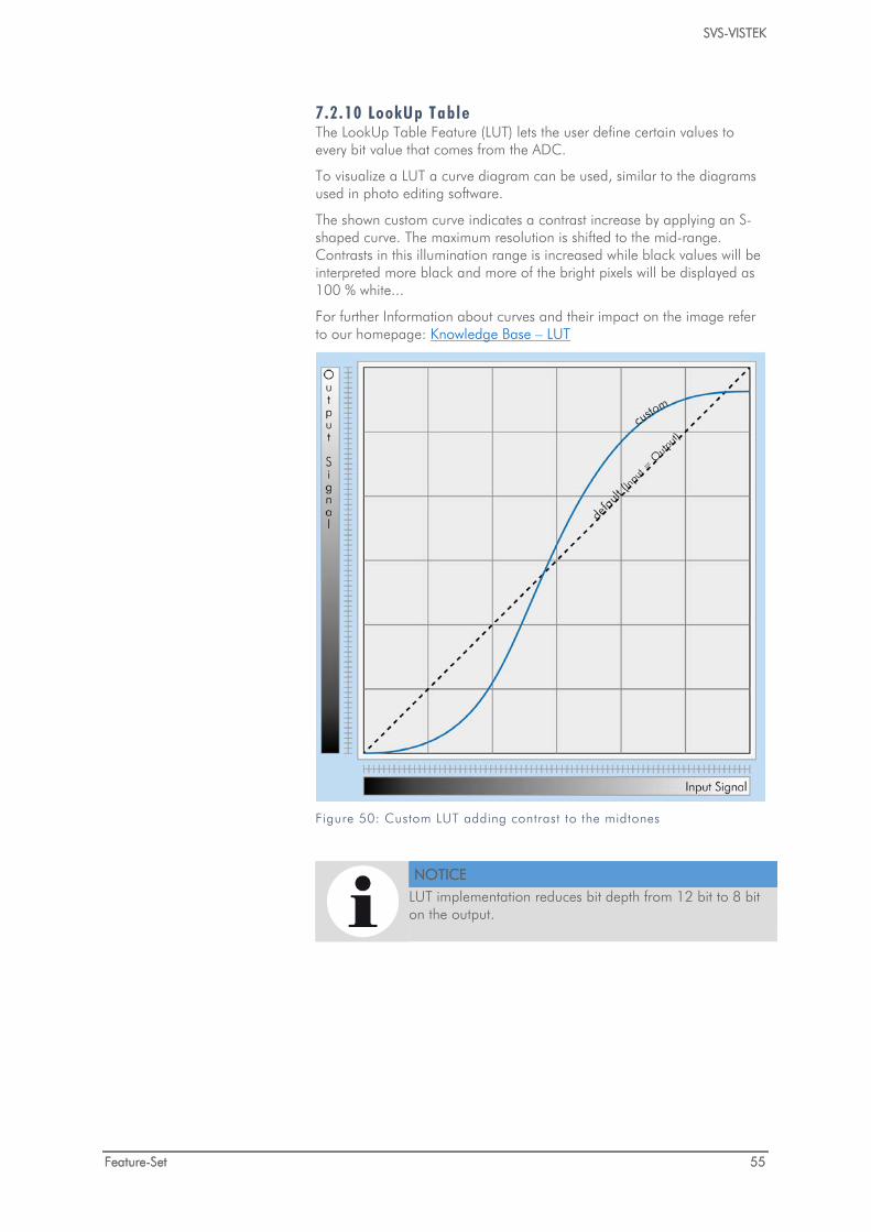
7.2.10 LookUp Table The LookUp Table Feature (LUT) lets the user define certain values to every bit value that comes from the ADC.
To visualize a LUT a curve diagram can be used, similar to the diagrams used in photo editing software.
The shown custom curve indicates a contrast increase by applying an S-shaped curve. The maximum resolution is shifted to the mid-range. Contrasts in this illumination range is increased while black values will be interpreted more black and more of the bright pixels will be displayed as 100 % white...
For further Information about curves and their impact on the image refer to our homepage: Knowledge Base – LUT
Figure 50: Custom LUT adding contrast to the midtones
NOTICE
LUT implementation reduces bit depth from 12 bit to 8 bit on the output.
SVS-VISTEK
Feature-Set 56
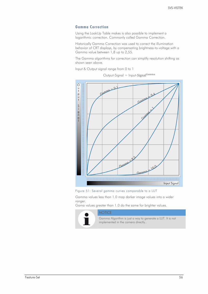
Gamma Correct ion Using the LookUp Table makes is also possible to implement a logarithmic correction. Commonly called Gamma Correction.
Historically Gamma Correction was used to correct the illumination behavior of CRT displays, by compensating brightness-to-voltage with a Gamma value between 1,8 up to 2,55.
The Gamma algorithms for correction can simplify resolution shifting as shown seen above.
Input & Output signal range from 0 to 1
Output-Signal = Input-SignalGamma
Figure 51: Several gamma curves comparable to a LUT
Gamma values less than 1.0 map darker image values into a wider ranger. Gama values greater than 1.0 do the same for brighter values.
NOTICE
Gamma Algorithm is just a way to generate a LUT. It is not implemented in the camera directly..
SVS-VISTEK
Feature-Set 57
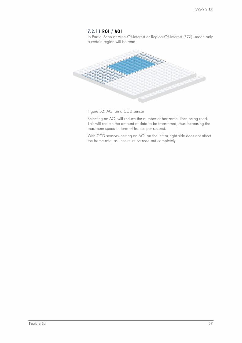
7.2.11 ROI / AOI In Partial Scan or Area-Of-Interest or Region-Of-Interest (ROI) -mode only a certain region will be read.
Figure 52: AOI on a CCD sensor
Selecting an AOI will reduce the number of horizontal lines being read. This will reduce the amount of data to be transferred, thus increasing the maximum speed in term of frames per second.
With CCD sensors, setting an AOI on the left or right side does not affect the frame rate, as lines must be read out completely.
SVS-VISTEK
Feature-Set 58
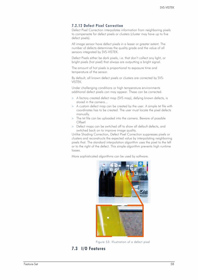
7.2.12 Defect Pixel Correct ion Defect Pixel Correction interpolates information from neighboring pixels to compensate for defect pixels or clusters (cluster may have up to five defect pixels).
All image sensor have defect pixels in a lesser or greater extent. The number of defects determines the quality grade and the value of all sensors integrated by SVS-VISTEK.
Defect Pixels either be dark pixels, i.e. that don’t collect any light, or bright pixels (hot pixel) that always are outputting a bright signal.
The amount of hot pixels is proportional to exposure time and temperature of the sensor.
By default, all known defect pixels or clusters are corrected by SVS-VISTEK.
Under challenging conditions or high temperature environments additional defect pixels can may appear. These can be corrected.
> A factory created defect map (SVS map), defying known defects, is stored in the camera...
> A custom defect map can be created by the user. A simple txt file with coordinates has to be created. The user must locate the pixel defects manually.
> The txt file can be uploaded into the camera. Beware of possible Offset!
> Defect maps can be switched off to show all default defects, and switched back on to improve image quality.
Unlike Shading Correction, Defect Pixel Correction suppresses pixels or clusters and reconstructs the expected value by interpolating neighboring pixels that. The standard interpolation algorithm uses the pixel to the left or to the right of the defect. This simple algorithm prevents high runtime losses.
More sophisticated algorithms can be used by software.
Figure 53: Illustration of a defect pixel
7.3 I/O Features
SVS-VISTEK
Feature-Set 59
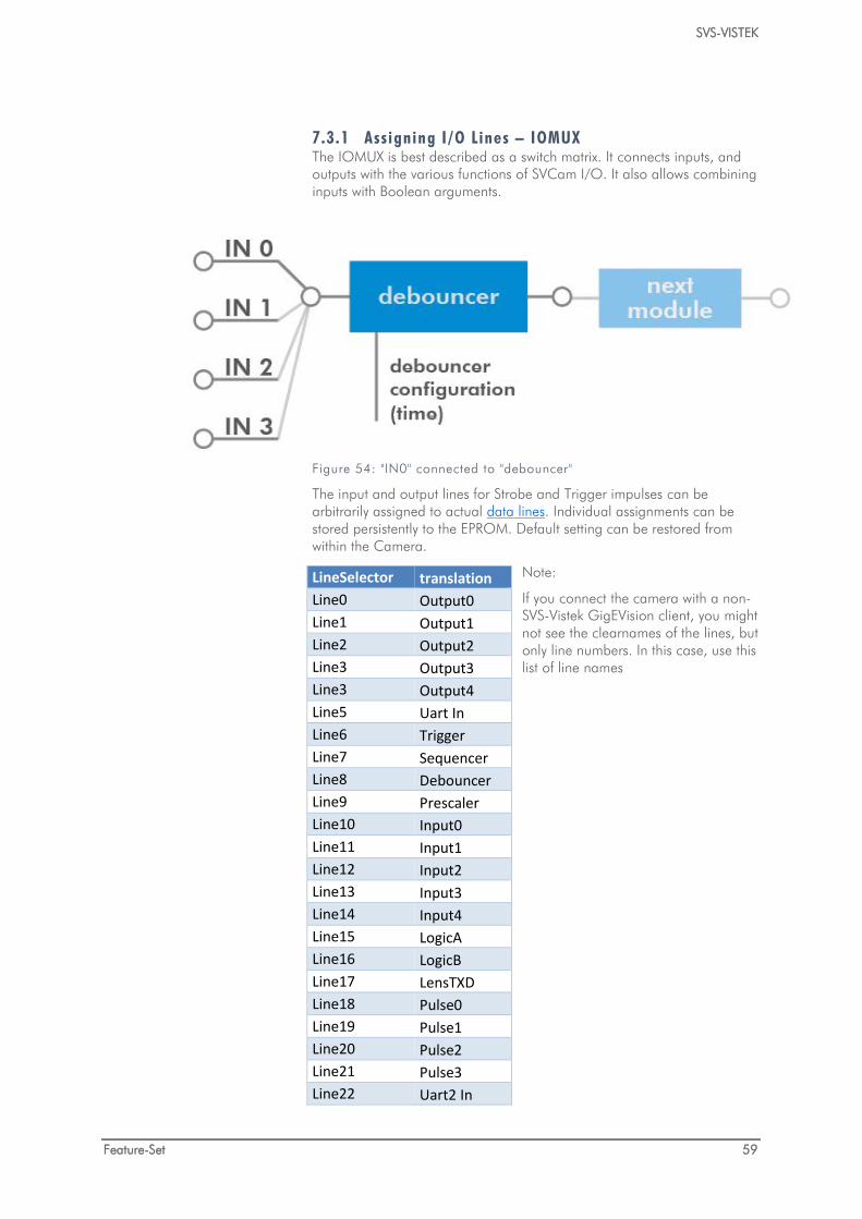
7.3.1 Assigning I/O Lines – IOMUX The IOMUX is best described as a switch matrix. It connects inputs, and outputs with the various functions of SVCam I/O. It also allows combining inputs with Boolean arguments.
Figure 54: "IN0" connected to "debouncer"
The input and output lines for Strobe and Trigger impulses can be arbitrarily assigned to actual data lines. Individual assignments can be stored persistently to the EPROM. Default setting can be restored from within the Camera.
Note:
If you connect the camera with a non-SVS-Vistek GigEVision client, you might not see the clearnames of the lines, but only line numbers. In this case, use this list of line names
LineSelector translation Line0 Output0 Line1 Output1 Line2 Output2 Line3 Output3 Line3 Output4 Line5 Uart In Line6 Trigger Line7 Sequencer Line8 Debouncer Line9 Prescaler Line10 Input0 Line11 Input1 Line12 Input2 Line13 Input3 Line14 Input4 Line15 LogicA Line16 LogicB Line17 LensTXD Line18 Pulse0 Line19 Pulse1 Line20 Pulse2 Line21 Pulse3 Line22 Uart2 In
SVS-VISTEK
Feature-Set 60
Refer to pinout in input / output connectors when physically wiring.
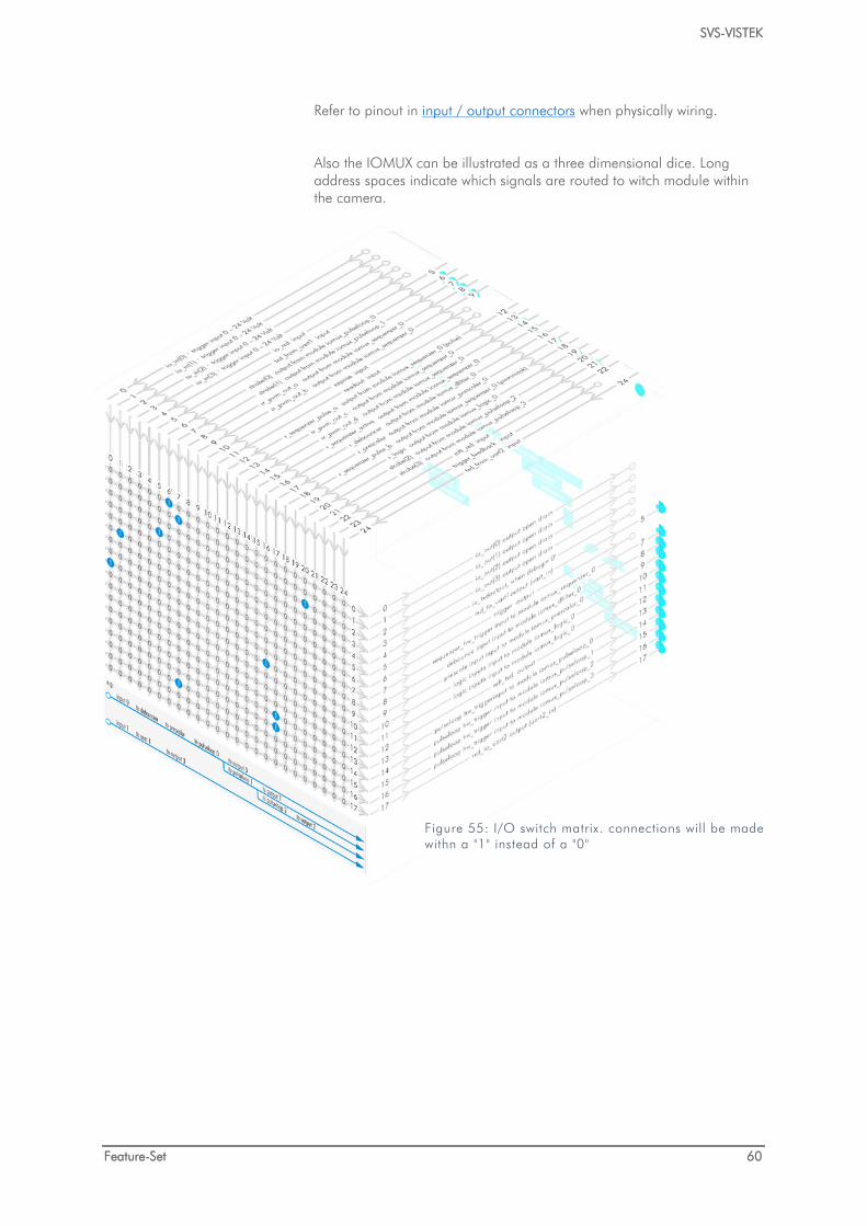
Also the IOMUX can be illustrated as a three dimensional dice. Long address spaces indicate which signals are routed to witch module within the camera.
Figure 55: I/O switch matrix. connections will be made withn a "1" instead of a "0"
SVS-VISTEK
Feature-Set 61
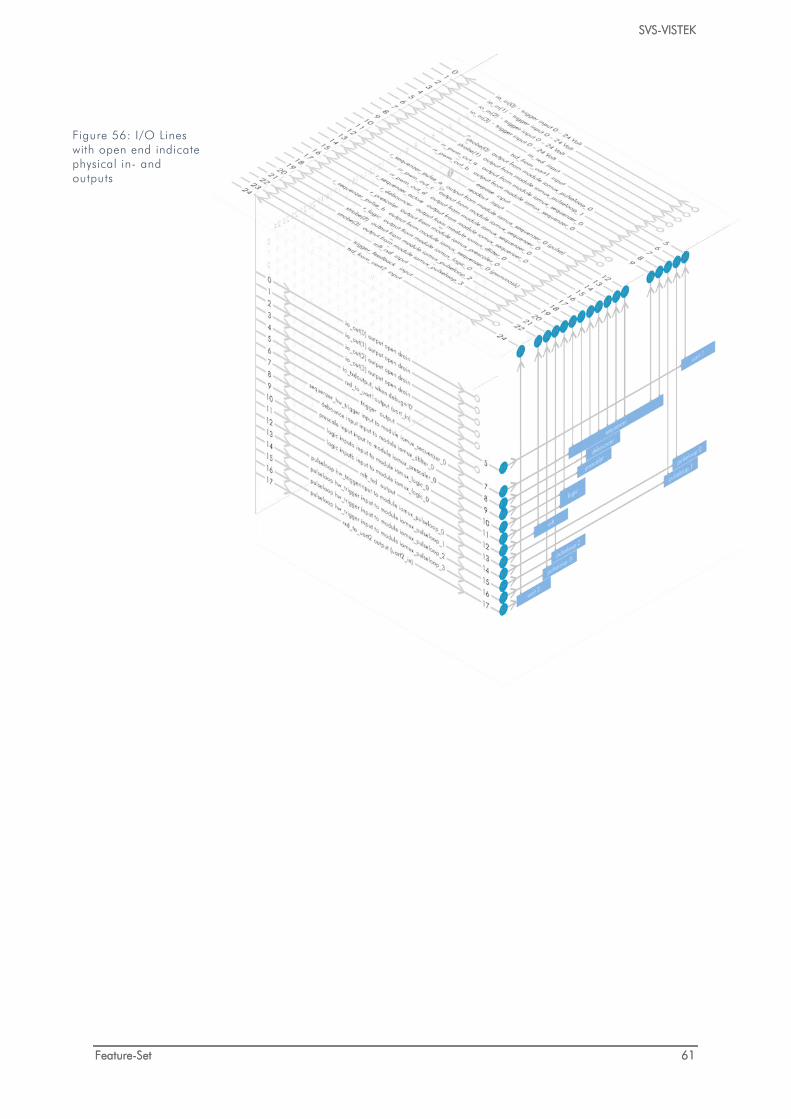
Figure 56: I/O Lines with open end indicate physical in- and outputs
SVS-VISTEK
Feature-Set 62
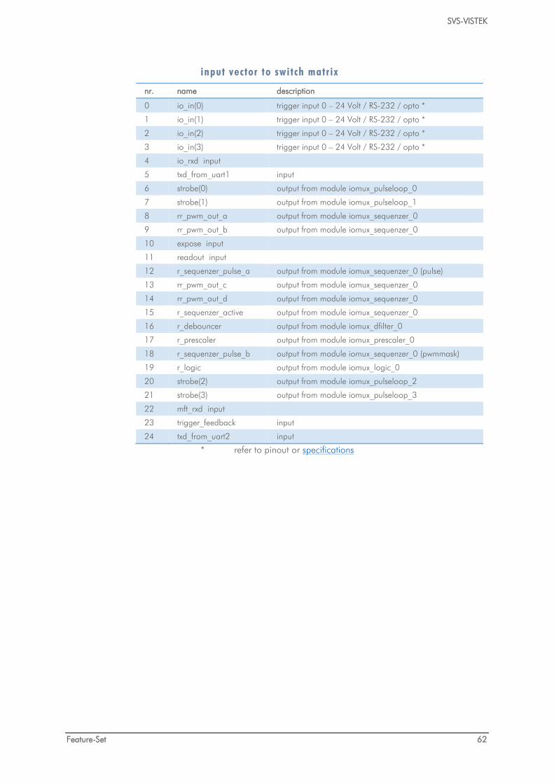
input vector to switch matrix
nr. name description
0 io_in(0) trigger input 0 – 24 Volt / RS-232 / opto *
1 io_in(1) trigger input 0 – 24 Volt / RS-232 / opto *
2 io_in(2) trigger input 0 – 24 Volt / RS-232 / opto *
3 io_in(3) trigger input 0 – 24 Volt / RS-232 / opto *
4 io_rxd input
5 txd_from_uart1 input
6 strobe(0) output from module iomux_pulseloop_0
7 strobe(1) output from module iomux_pulseloop_1
8 rr_pwm_out_a output from module iomux_sequenzer_0
9 rr_pwm_out_b output from module iomux_sequenzer_0
10 expose input
11 readout input
12 r_sequenzer_pulse_a output from module iomux_sequenzer_0 (pulse)
13 rr_pwm_out_c output from module iomux_sequenzer_0
14 rr_pwm_out_d output from module iomux_sequenzer_0
15 r_sequenzer_active output from module iomux_sequenzer_0
16 r_debouncer output from module iomux_dfilter_0
17 r_prescaler output from module iomux_prescaler_0
18 r_sequenzer_pulse_b output from module iomux_sequenzer_0 (pwmmask)
19 r_logic output from module iomux_logic_0
20 strobe(2) output from module iomux_pulseloop_2
21 strobe(3) output from module iomux_pulseloop_3
22 mft_rxd input
23 trigger_feedback input
24 txd_from_uart2 input
* refer to pinout or specifications
SVS-VISTEK
Feature-Set 63
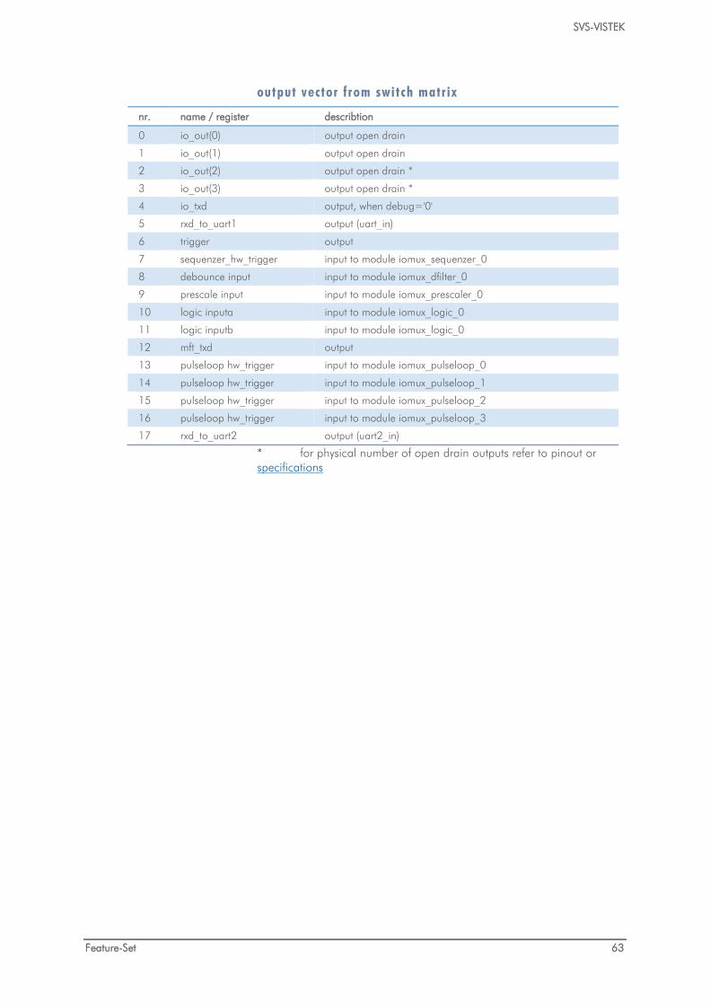
output vector from switch matrix
nr. name / register describtion
0 io_out(0) output open drain
1 io_out(1) output open drain
2 io_out(2) output open drain *
3 io_out(3) output open drain *
4 io_txd output, when debug='0'
5 rxd_to_uart1 output (uart_in)
6 trigger output
7 sequenzer_hw_trigger input to module iomux_sequenzer_0
8 debounce input input to module iomux_dfilter_0
9 prescale input input to module iomux_prescaler_0
10 logic inputa input to module iomux_logic_0
11 logic inputb input to module iomux_logic_0
12 mft_txd output
13 pulseloop hw_trigger input to module iomux_pulseloop_0
14 pulseloop hw_trigger input to module iomux_pulseloop_1
15 pulseloop hw_trigger input to module iomux_pulseloop_2
16 pulseloop hw_trigger input to module iomux_pulseloop_3
17 rxd_to_uart2 output (uart2_in)
* for physical number of open drain outputs refer to pinout or specifications
SVS-VISTEK
Feature-Set 64
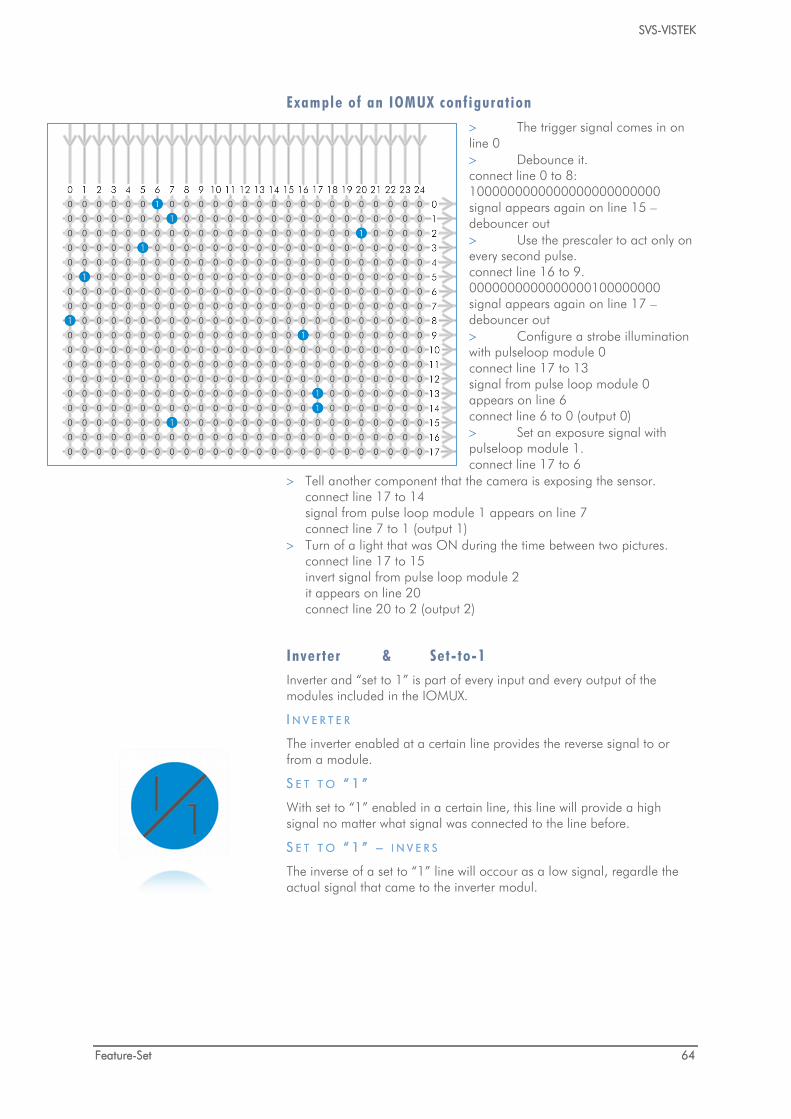
Example of an IOMUX configuration
> The trigger signal comes in on line 0 > Debounce it. connect line 0 to 8: 1000000000000000000000000 signal appears again on line 15 – debouncer out > Use the prescaler to act only on every second pulse. connect line 16 to 9. 0000000000000000100000000 signal appears again on line 17 – debouncer out > Configure a strobe illumination with pulseloop module 0 connect line 17 to 13 signal from pulse loop module 0 appears on line 6 connect line 6 to 0 (output 0) > Set an exposure signal with pulseloop module 1. connect line 17 to 6
> Tell another component that the camera is exposing the sensor. connect line 17 to 14 signal from pulse loop module 1 appears on line 7 connect line 7 to 1 (output 1)
> Turn of a light that was ON during the time between two pictures. connect line 17 to 15 invert signal from pulse loop module 2 it appears on line 20 connect line 20 to 2 (output 2)
Inverter & Set-to-1 Inverter and “set to 1” is part of every input and every output of the modules included in the IOMUX.
I N V E R T E R
The inverter enabled at a certain line provides the reverse signal to or from a module.
S E T T O “ 1 ”
With set to “1” enabled in a certain line, this line will provide a high signal no matter what signal was connected to the line before.
S E T T O “ 1 ” – I N V E R S
The inverse of a set to “1” line will occour as a low signal, regardle the actual signal that came to the inverter modul.
SVS-VISTEK
Feature-Set 65
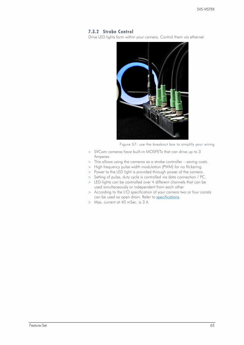
7.3.2 Strobe Control Drive LED lights form within your camera. Control them via ethernet.
Figure 57: use the breakout box to simplify your wiring
> SVCam cameras have built-in MOSFETs that can drive up to 3 Amperes.
> This allows using the cameras as a strobe controller – saving costs. > High frequency pulse width modulation (PWM) for no flickering. > Power to the LED light is provided through power of the camera. > Setting of pulse, duty cycle is controlled via data connection / PC. > LED-lights can be controlled over 4 different channels that can be
used simultaneously or independent from each other > According to the I/O specification of your camera two or four canals
can be used as open drain. Refer to specifications. > Max. current at 40 mSec. is 3 A
SVS-VISTEK
Feature-Set 66
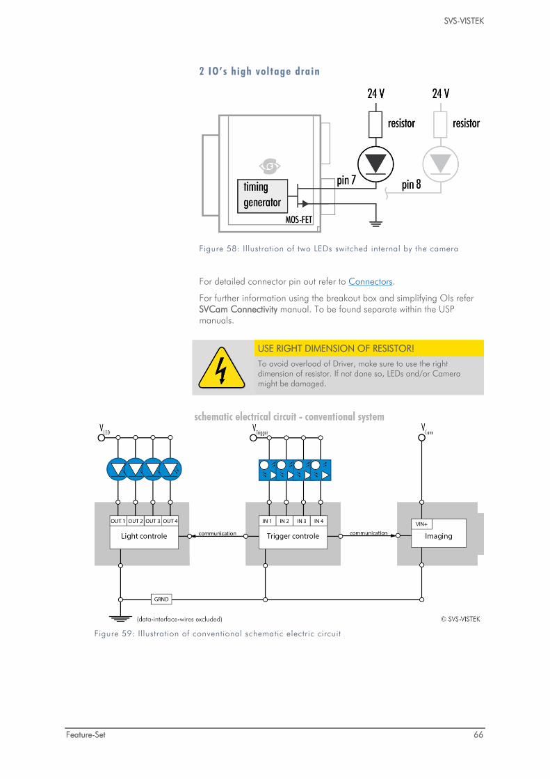
2 IO’s high voltage drain
Figure 58: Illustration of two LEDs switched internal by the camera
For detailed connector pin out refer to Connectors.
For further information using the breakout box and simplifying OIs refer SVCam Connectivity manual. To be found separate within the USP manuals.
Figure 59: Illustration of conventional schematic electric circuit
USE RIGHT DIMENSION OF RESISTOR!
To avoid overload of Driver, make sure to use the right dimension of resistor. If not done so, LEDs and/or Camera might be damaged.
SVS-VISTEK
Feature-Set 67
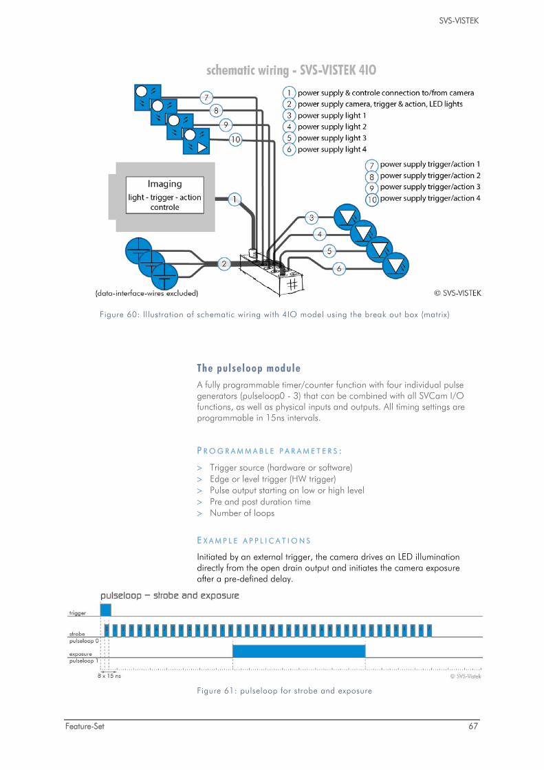
Figure 60: Illustration of schematic wiring with 4IO model using the break out box (matrix)
The pulseloop module A fully programmable timer/counter function with four individual pulse generators (pulseloop0 - 3) that can be combined with all SVCam I/O functions, as well as physical inputs and outputs. All timing settings are programmable in 15ns intervals.
P R O G R A M M A B L E P A R A M E T E R S :
> Trigger source (hardware or software) > Edge or level trigger (HW trigger) > Pulse output starting on low or high level > Pre and post duration time > Number of loops
E X A M P L E A P P L I C A T I O N S
Initiated by an external trigger, the camera drives an LED illumination directly from the open drain output and initiates the camera exposure after a pre-defined delay.
Figure 61: pulseloop for strobe and exposure
SVS-VISTEK
Feature-Set 68
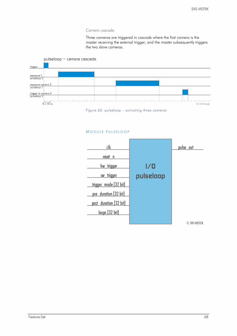
Camera cascade
Three cameras are triggered in cascade where the first camera is the master receiving the external trigger, and the master subsequently triggers the two slave cameras.
Figure 62: pulseloop – activating three cameras
M O D U L E P U L S E L O O P
SVS-VISTEK
Feature-Set 69
LEDs in Continuous Mode
Example Calculation “No Flash” (CW Mode)
Voltage drop al 5 LEDs, 2,2 V per LED (see spec. of LED) 11 V
Max. continuous current (see spec. of LED) 250 mA
Voltage Supply 24 V
Voltage drop at Resistor (24 V – 11 V) 13 V
Pull up Resistor R = 𝟏𝟏 𝑽𝟐𝟐𝟐 𝒎𝒎
52 Ω
Total Power ( 𝑷 = 𝑼 × 𝑰 ) 6 W
Power at LEDs (𝟏𝟏 𝑽 × 𝟐𝟐𝟐 𝒎𝒎) 2,75 W
Power Loss at Resistor ( 𝟏𝟏 𝑽 × 𝟐𝟐𝟐 𝒎𝒎 ) 3,25 W
LEDs in Flash Mode The MOS FETs at “OUT1” and “OUT2” are used like a “switch”. By controlling “on time” and “off time” (duty cycle) the intensity of light and current can be controlled.
Current “time ON” within a 1 Sec PWM %
0,75 A 500 ms 50 %
1 A 300 ms 33,3 %
2 A 70 ms 7 %
3 A 40 ms 4 %
Example: If pulse is 1.5 A the max. “on” time is 150 mSec. This means the “off” time is 850 mSec. The sum of “time on” and “time off” is 1000 mSec = 1 Sec.
NOTICE
The shorter the „time on“ – the higher current can be used –the longer LEDs will work.
SVS-VISTEK
Feature-Set 70
Strobe Timing
Exposu re De l ay
A value, representing the time between the (logical) positive edge of trigger pulse and start of integration time. Unit is 1μs. Default is 0μs.
S t r obe Po lar i ty
Positive or negative polarity of the hardware strobe output can be selected.
S t r obe Dura t ion
The exposure time of LED lights can be set in µsec. The min duration is 1 µsec. The longest time is 1 second.
S t r obe De lay
The delay between the (logical) positive edge of trigger pulse and strobe pulse output can be set in µsec. Unit is 1μs. Default is 0μs.
SVS-VISTEK
Feature-Set 71
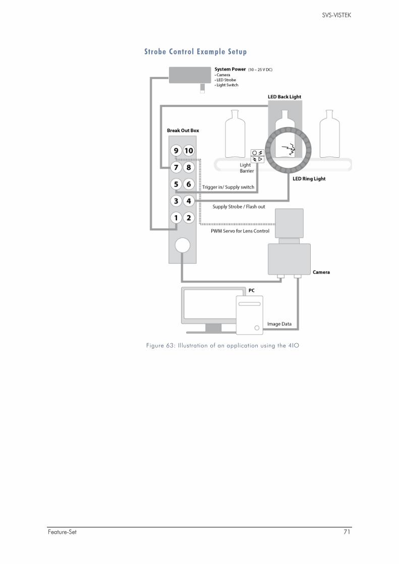
Strobe Control Example Setup
Figure 63: Illustration of an application using the 4IO
SVS-VISTEK
Feature-Set 72
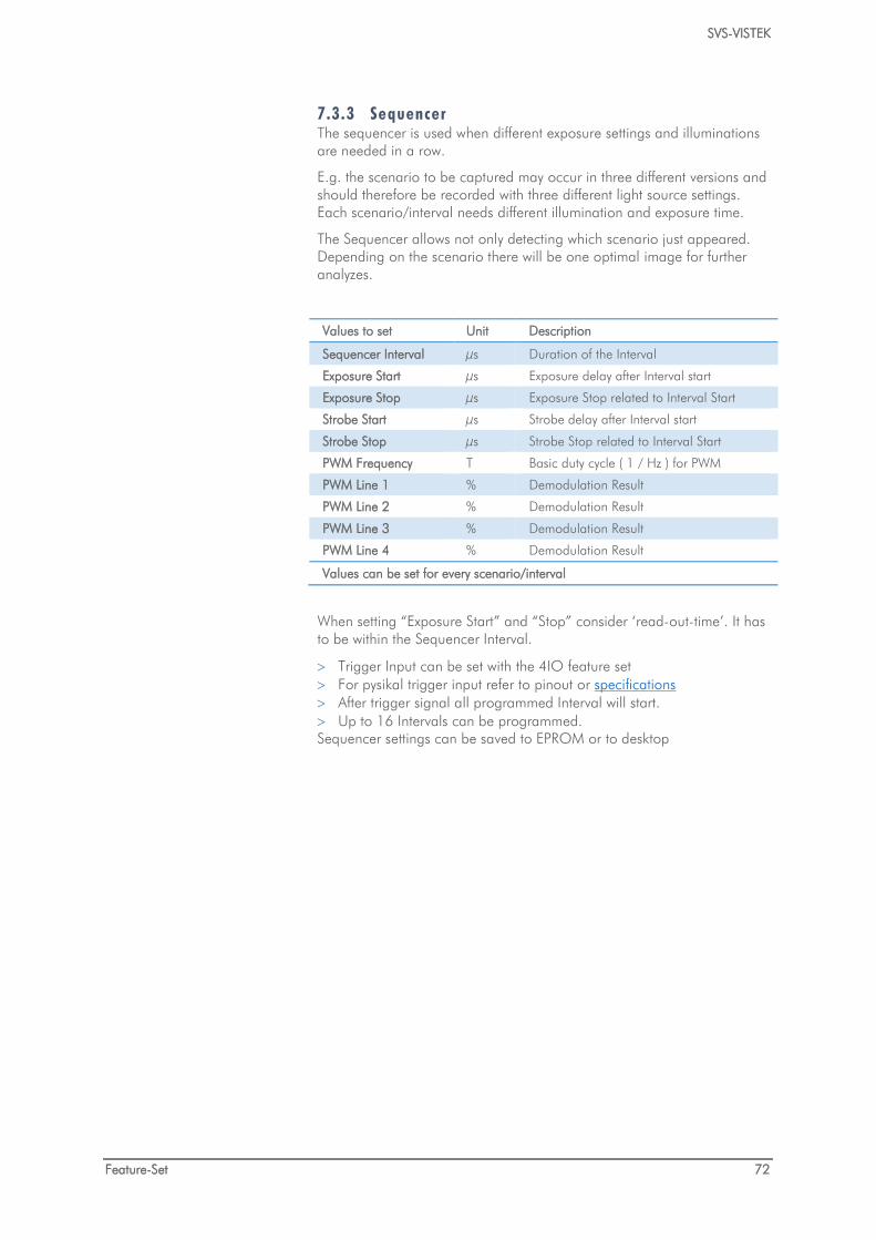
7.3.3 Sequencer The sequencer is used when different exposure settings and illuminations are needed in a row.
E.g. the scenario to be captured may occur in three different versions and should therefore be recorded with three different light source settings. Each scenario/interval needs different illumination and exposure time.
The Sequencer allows not only detecting which scenario just appeared. Depending on the scenario there will be one optimal image for further analyzes.
Values to set Unit Description
Sequencer Interval µs Duration of the Interval
Exposure Start µs Exposure delay after Interval start
Exposure Stop µs Exposure Stop related to Interval Start
Strobe Start µs Strobe delay after Interval start
Strobe Stop µs Strobe Stop related to Interval Start
PWM Frequency T Basic duty cycle ( 1 / Hz ) for PWM
PWM Line 1 % Demodulation Result
PWM Line 2 % Demodulation Result
PWM Line 3 % Demodulation Result
PWM Line 4 % Demodulation Result
Values can be set for every scenario/interval
When setting “Exposure Start” and “Stop” consider ‘read-out-time’. It has to be within the Sequencer Interval.
> Trigger Input can be set with the 4IO feature set > For pysikal trigger input refer to pinout or specifications > After trigger signal all programmed Interval will start. > Up to 16 Intervals can be programmed. Sequencer settings can be saved to EPROM or to desktop
SVS-VISTEK
Feature-Set 73
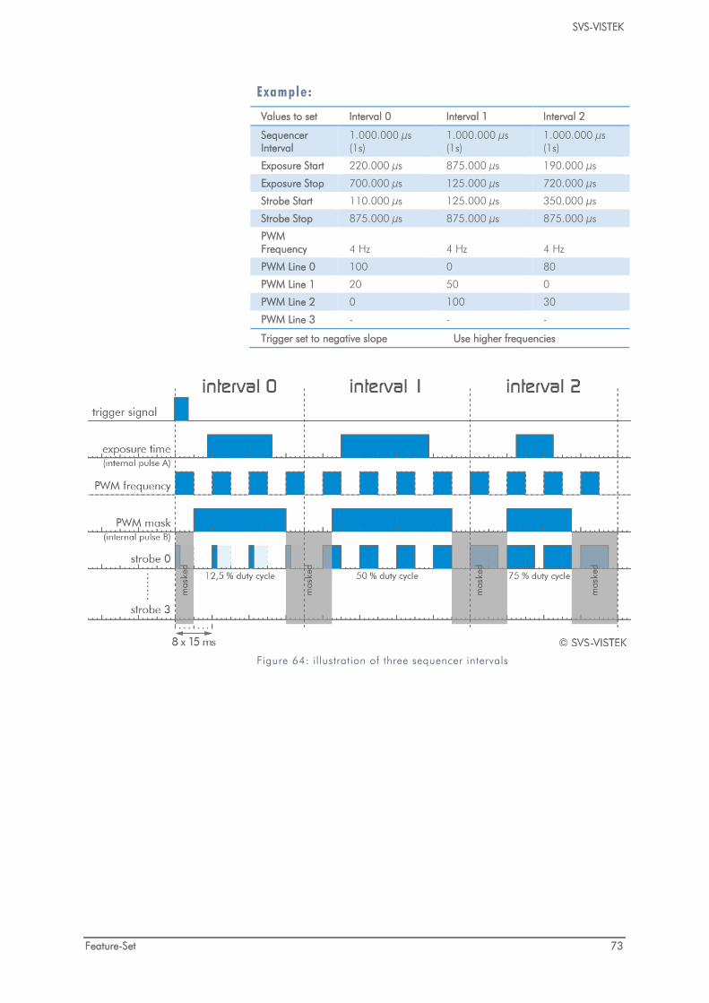
Example:
Values to set Interval 0 Interval 1 Interval 2
Sequencer Interval
1.000.000 µs (1s)
1.000.000 µs (1s)
1.000.000 µs (1s)
Exposure Start 220.000 µs 875.000 µs 190.000 µs
Exposure Stop 700.000 µs 125.000 µs 720.000 µs
Strobe Start 110.000 µs 125.000 µs 350.000 µs
Strobe Stop 875.000 µs 875.000 µs 875.000 µs
PWM Frequency 4 Hz 4 Hz 4 Hz
PWM Line 0 100 0 80
PWM Line 1 20 50 0
PWM Line 2 0 100 30
PWM Line 3 - - -
Trigger set to negative slope Use higher frequencies
Figure 64: illustration of three sequencer intervals
SVS-VISTEK
Feature-Set 74
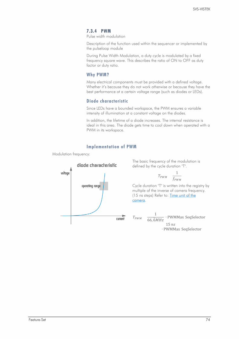
7.3.4 PWM Pulse width modulation
Description of the function used within the sequencer or implemented by the pulseloop module
During Pulse Width Modulation, a duty cycle is modulated by a fixed frequency square wave. This describes the ratio of ON to OFF as duty factor or duty ratio.
Why PWM? Many electrical components must be provided with a defined voltage. Whether it’s because they do not work otherwise or because they have the best performance at a certain voltage range (such as diodes or LEDs).
Diode characteri st ic Since LEDs have a bounded workspace, the PWM ensures a variable intensity of illumination at a constant voltage on the diodes.
In addition, the lifetime of a diode increases. The internal resistance is ideal in this area. The diode gets time to cool down when operated with a PWM in its workspace.
Implementation of PWM Modulation frequency:
The basic frequency of the modulation is defined by the cycle duration "T".
𝑇𝑃𝑃𝑃 =1
𝑓𝑃𝑃𝑃
Cycle duration "T" is written into the registry by multiple of the inverse of camera frequency. (15 ns steps) Refer to: Time unit of the camera.
𝑇𝑃𝑃𝑃 =1
66, 6𝑀𝑀𝑀 ∙ PWMMax[SeqSelector]
= 15 𝑛𝑠 ∙ PWMMax[SeqSelector]
SVS-VISTEK
Feature-Set 75
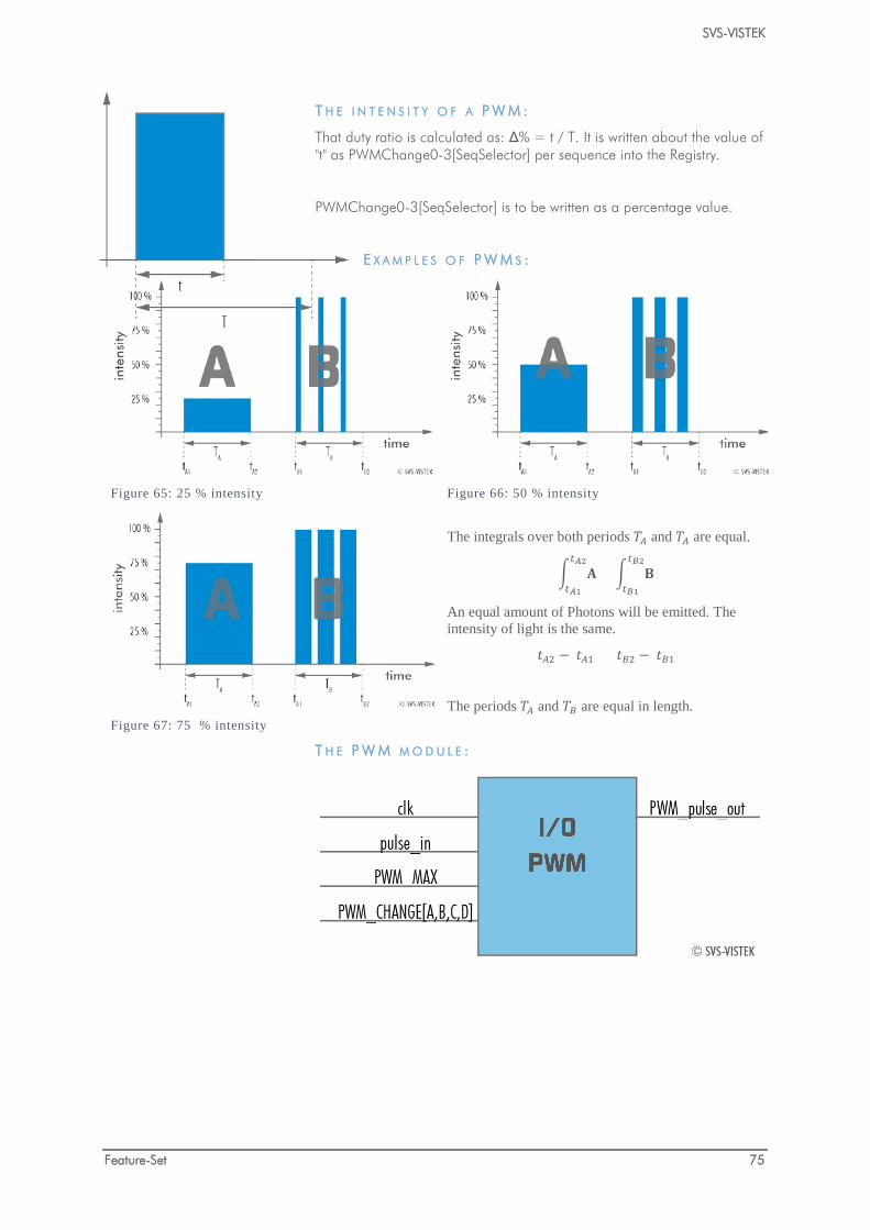
T H E I N T E N S I T Y O F A P W M :
That duty ratio is calculated as: Δ% = t / T. It is written about the value of "t" as PWMChange0-3[SeqSelector] per sequence into the Registry.
PWMChange0-3[SeqSelector] is to be written as a percentage value.
E X A M P L E S O F P W M S :
Figure 65: 25 % intensity
Figure 66: 50 % intensity
Figure 67: 75 % intensity
The integrals over both periods 𝑇𝐴 and 𝑇𝐴 are equal.
𝐀𝑡𝐴2
𝑡𝐴1= 𝐁
𝑡𝐵2
𝑡𝐵1
An equal amount of Photons will be emitted. The intensity of light is the same.
𝑡𝐴2 − 𝑡𝐴1 = 𝑡𝐵2 − 𝑡𝐵1
The periods 𝑇𝐴 and 𝑇𝐵 are equal in length.
T H E P W M M O D U L E :
SVS-VISTEK
Feature-Set 76
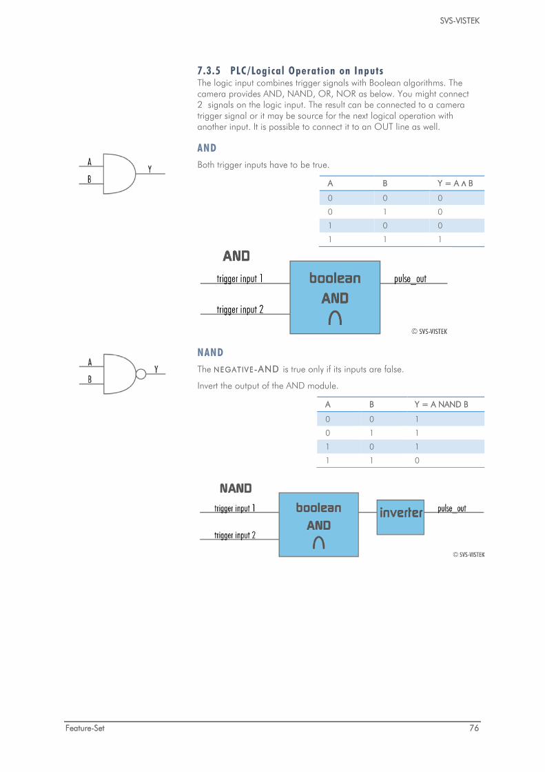
7.3.5 PLC/Logical Operation on Inputs The logic input combines trigger signals with Boolean algorithms. The camera provides AND, NAND, OR, NOR as below. You might connect 2 signals on the logic input. The result can be connected to a camera trigger signal or it may be source for the next logical operation with another input. It is possible to connect it to an OUT line as well.
AND Both trigger inputs have to be true.
A B Y = A ∧ B
0 0 0
0 1 0
1 0 0
1 1 1
NAND The NEGAT IVE-AND is true only if its inputs are false.
Invert the output of the AND module.
A B Y = A NAND B
0 0 1
0 1 1
1 0 1
1 1 0
SVS-VISTEK
Feature-Set 77
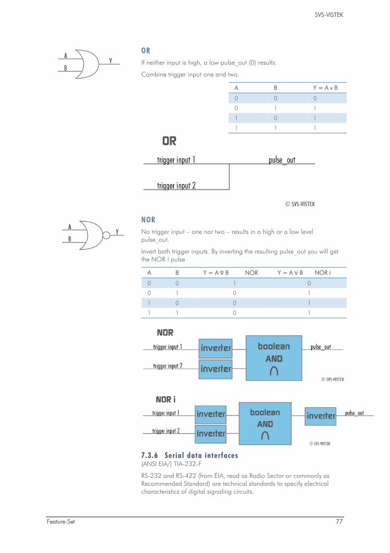
OR If neither input is high, a low pulse_out (0) results.
Combine trigger input one and two.
A B Y = A v B
0 0 0
0 1 1
1 0 1
1 1 1
NOR No trigger input – one nor two – results in a high or a low level pulse_out.
Invert both trigger inputs. By inverting the resulting pulse_out you will get the NOR I pulse
A B Y = A ⊽ B NOR Y = A ∨ B NOR i
0 0 1 0
0 1 0 1
1 0 0 1
1 1 0 1
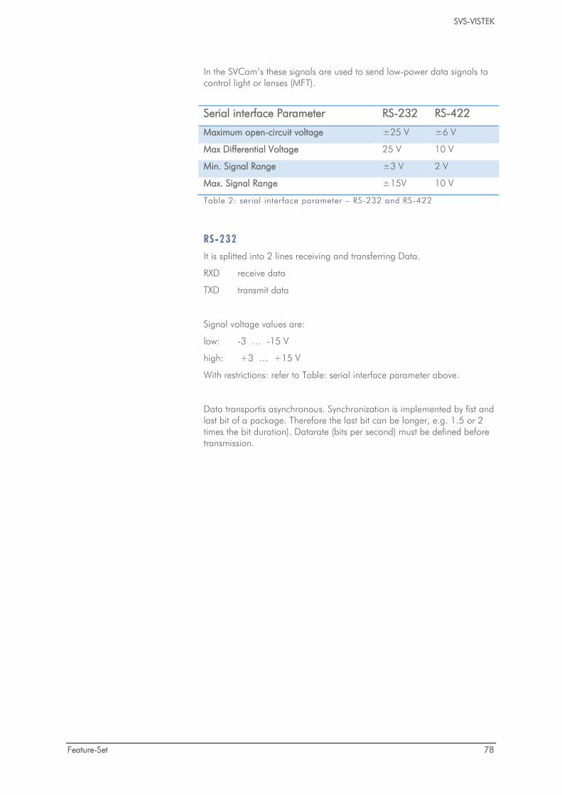
7.3.6 Serial data interfaces (ANSI EIA/) TIA-232-F
RS-232 and RS-422 (from EIA, read as Radio Sector or commonly as Recommended Standard) are technical standards to specify electrical characteristics of digital signaling circuits.
SVS-VISTEK
Feature-Set 78
In the SVCam’s these signals are used to send low-power data signals to control light or lenses (MFT).
Table 2: serial interface parameter – RS-232 and RS-422
RS-232 It is splitted into 2 lines receiving and transferring Data.
RXD receive data
TXD transmit data
Signal voltage values are:
low: -3 … -15 V
high: +3 … +15 V
With restrictions: refer to Table: serial interface parameter above.
Data transportis asynchronous. Synchronization is implemented by fist and last bit of a package. Therefore the last bit can be longer, e.g. 1.5 or 2 times the bit duration). Datarate (bits per second) must be defined before transmission.
Serial interface Parameter RS-232 RS-422
Maximum open-circuit voltage ±25 V ±6 V
Max Differential Voltage 25 V 10 V
Min. Signal Range ±3 V 2 V
Max. Signal Range ±15V 10 V
SVS-VISTEK
Feature-Set 79
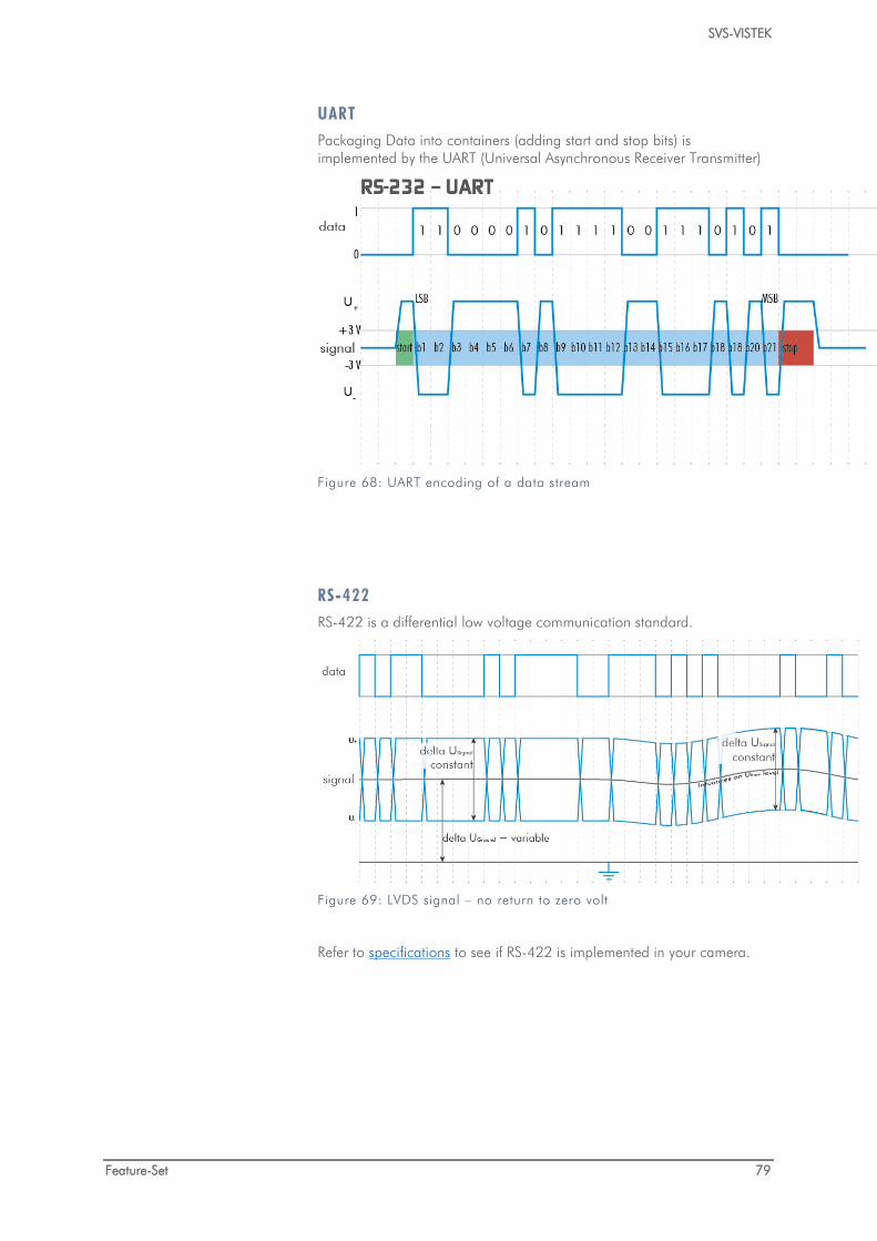
UART Packaging Data into containers (adding start and stop bits) is implemented by the UART (Universal Asynchronous Receiver Transmitter)
Figure 68: UART encoding of a data stream
RS-422 RS-422 is a differential low voltage communication standard.
Figure 69: LVDS signal – no return to zero volt
Refer to specifications to see if RS-422 is implemented in your camera.
SVS-VISTEK
Feature-Set 80
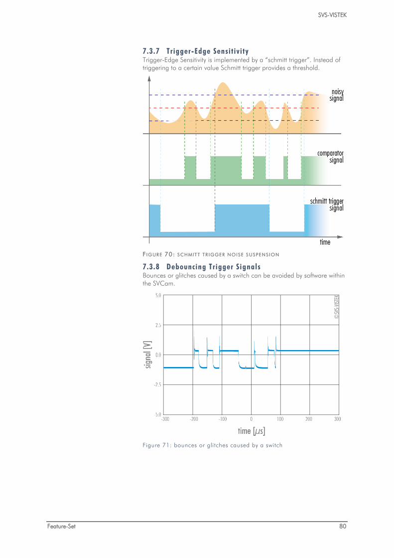
7.3.7 Trigger-Edge Sensit ivi ty Trigger-Edge Sensitivity is implemented by a “schmitt trigger”. Instead of triggering to a certain value Schmitt trigger provides a threshold.
F I G UR E 70: S C H M IT T TR I G GER N OI SE S U SPE N S I ON
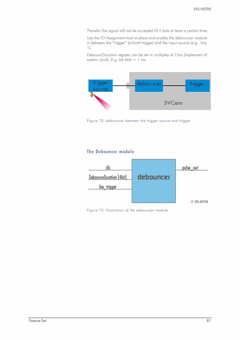
7.3.8 Debouncing Trigger Signals Bounces or glitches caused by a switch can be avoided by software within the SVCam.
Figure 71: bounces or glitches caused by a switch
SVS-VISTEK
Feature-Set 81
Therefor the signal will not be accepted till it lasts at least a certain time.
Use the IO Assignment tool to place and enable the debouncer module in between the “trigger” (schmitt trigger) and the input source (e.g.: line 1).
DebouncDuration register can be set in multiples of 15ns (implement of system clock). E.g. 66 666 ≈ 1 ms
Figure 72: debouncer between the trigger source and trigger
The Debouncer module
Figure 73: Illustration of the debouncer module
SVS-VISTEK
Feature-Set 82
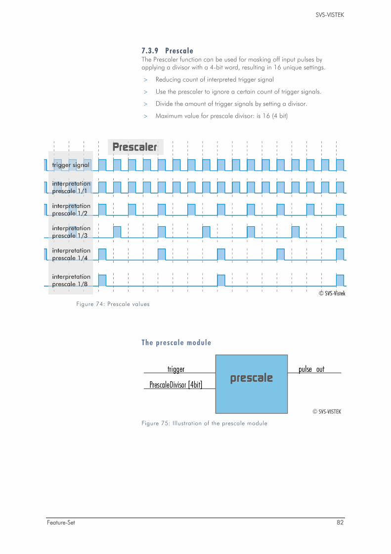
7.3.9 Prescale The Prescaler function can be used for masking off input pulses by applying a divisor with a 4-bit word, resulting in 16 unique settings.
> Reducing count of interpreted trigger signal
> Use the prescaler to ignore a certain count of trigger signals.
> Divide the amount of trigger signals by setting a divisor.
> Maximum value for prescale divisor: is 16 (4 bit)
Figure 74: Prescale values
The prescale module
Figure 75: Illustration of the prescale module
SVS-VISTEK
Feature-Set 83
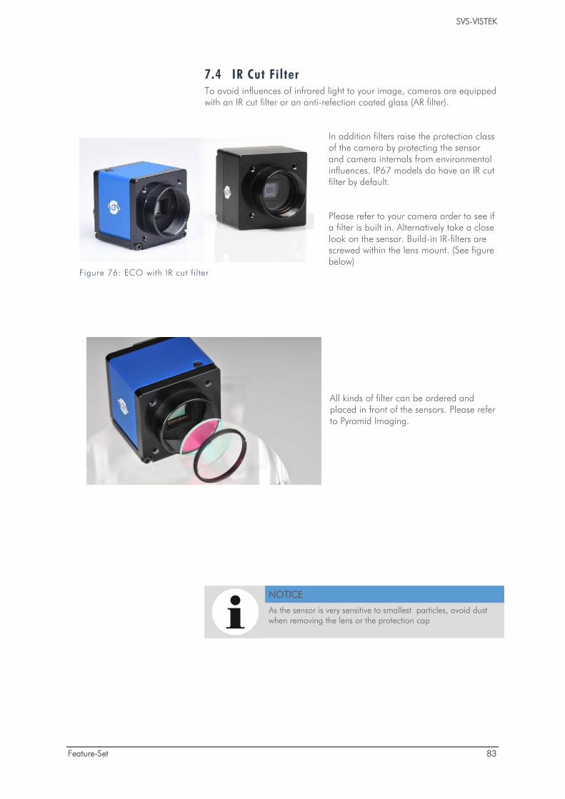
Figure 76: ECO with IR cut filter
7.4 IR Cut Filter To avoid influences of infrared light to your image, cameras are equipped with an IR cut filter or an anti-refection coated glass (AR filter).
In addition filters raise the protection class of the camera by protecting the sensor and camera internals from environmental influences. IP67 models do have an IR cut filter by default.
Please refer to your camera order to see if a filter is built in. Alternatively take a close look on the sensor. Build-in IR-filters are screwed within the lens mount. (See figure below)
All kinds of filter can be ordered and placed in front of the sensors. Please refer to Pyramid Imaging.
NOTICE
As the sensor is very sensitive to smallest particles, avoid dust when removing the lens or the protection cap
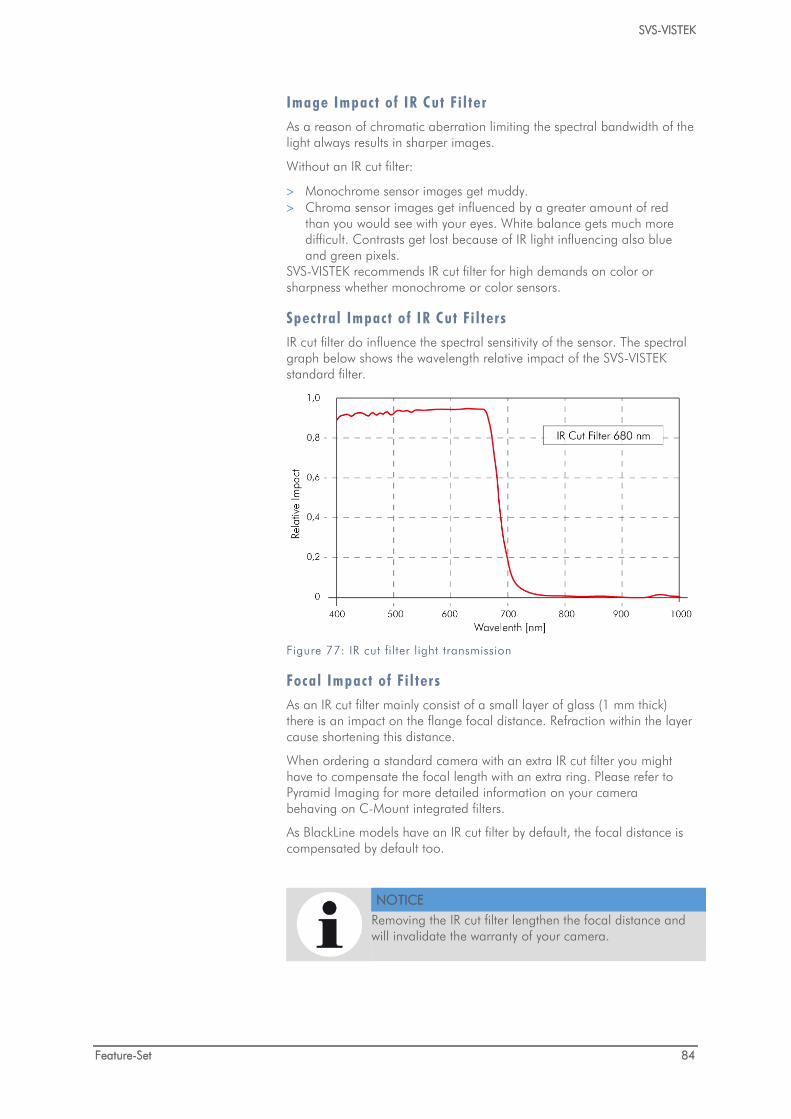
SVS-VISTEK
Feature-Set 84
Image Impact of IR Cut Fi l ter As a reason of chromatic aberration limiting the spectral bandwidth of the light always results in sharper images.
Without an IR cut filter:
> Monochrome sensor images get muddy. > Chroma sensor images get influenced by a greater amount of red
than you would see with your eyes. White balance gets much more difficult. Contrasts get lost because of IR light influencing also blue and green pixels.
SVS-VISTEK recommends IR cut filter for high demands on color or sharpness whether monochrome or color sensors.
Spectral Impact of IR Cut Fi l ters IR cut filter do influence the spectral sensitivity of the sensor. The spectral graph below shows the wavelength relative impact of the SVS-VISTEK standard filter.
Figure 77: IR cut filter light transmission
Focal Impact of Fi l ters As an IR cut filter mainly consist of a small layer of glass (1 mm thick) there is an impact on the flange focal distance. Refraction within the layer cause shortening this distance.
When ordering a standard camera with an extra IR cut filter you might have to compensate the focal length with an extra ring. Please refer to Pyramid Imaging for more detailed information on your camera behaving on C-Mount integrated filters.
As BlackLine models have an IR cut filter by default, the focal distance is compensated by default too.
NOTICE
Removing the IR cut filter lengthen the focal distance and will invalidate the warranty of your camera.
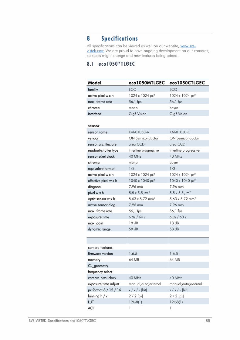
SVS-VISTEK–Specifications eco1050*TLGEC 85
8 Specifications All specifications can be viewed as well on our website, www.svs-vistek.com We are proud to have ongoing development on our cameras, so specs might change and new features being added.
8.1 eco1050*TLGEC
Model eco1050MTLGEC eco1050CTLGEC familiy ECO ECO
active pixel w x h 1024 x 1024 px² 1024 x 1024 px²
max. frame rate 56,1 fps 56,1 fps
chroma mono bayer
interface GigE Vision GigE Vision
sensor
sensor name KAI-01050-A KAI-01050-C
vendor ON Semiconductor ON Semiconductor
sensor architecture area CCD area CCD
readout/shutter type interline progressive interline progressive
sensor pixel clock 40 MHz 40 MHz
chroma mono bayer
equivalent format 1/2 1/2
active pixel w x h 1024 x 1024 px² 1024 x 1024 px²
effective pixel w x h 1040 x 1040 px² 1040 x 1040 px²
diagonal 7,96 mm 7,96 mm
pixel w x h 5,5 x 5,5 µm² 5,5 x 5,5 µm²
optic sensor w x h 5,63 x 5,72 mm² 5,63 x 5,72 mm²
active sensor diag. 7,96 mm 7,96 mm
max. frame rate 56,1 fps 56,1 fps
exposure time 6 µs / 60 s 6 µs / 60 s
max. gain 18 dB 18 dB
dynamic range 58 dB 58 dB
camera features
firmware version 1.6.5 1.6.5
memory 64 MB 64 MB
CL_geometry
frequency select
camera pixel clock 40 MHz 40 MHz
exposure time adjust manual;auto;external manual;auto;external
px format 8 / 12 / 16 x / x / - [bit] x / x / - [bit]
binning h / v 2 / 2 [px] 2 / 2 [px]
LUT 12to8(1) 12to8(1)
AOI 1 1
SVS-VISTEK
Specifications 86
white balancing auto;manual auto;manual
tap balancing manual;auto manual;auto
gain auto;manual auto;manual
offset manual manual
PIV mode
readout control manual;delayed manual;delayed
flat field correction
shading correction
defect pixel correction x x
I/O features
trigger modes internal;software;external internal;software;external
high low trigger x x
pulseloop 4 4
IOMUX pwm(4);sequencer pwm(4);sequencer
exposure output x x
trigger in 24 V 2 2
output open drain 2 2
opto input / output
RS-232 in / out 1 / 1 1 / 1
RS-422 in / out 1 / 1 1 / 1
housing features
Mount C-Mount C-Mount
lens control dimensions w / h / d mm³ 38 / 38 / 45 mm³ 38 / 38 / 45 mm³
weight 110 g 110 g
protection class IP40 IP40
temp. Sensor Mainboard Mainboard
temp. Ambient °C -10 to 45 °C -10 to 45 °C
© SVS-VISTEK Jan 29, 2018 Jan 29, 2018
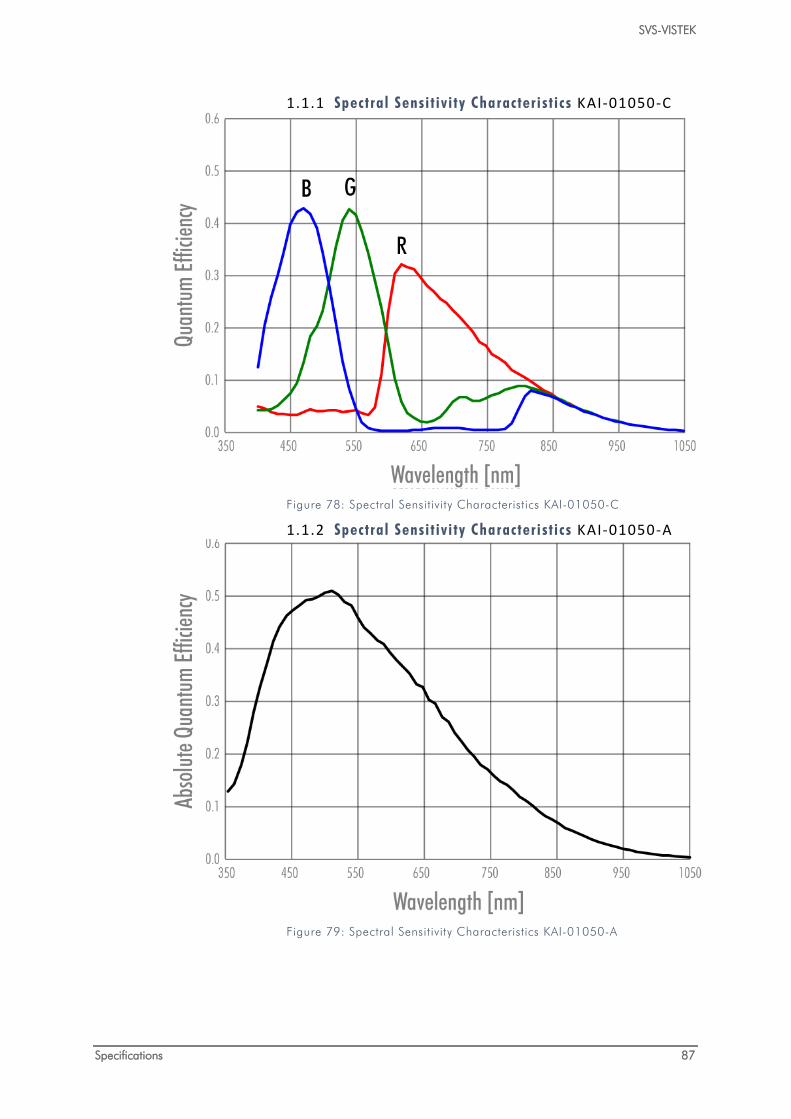
SVS-VISTEK
Specifications 87
1.1.1 Spectral Sensit ivi ty Characteri st ics KAI-01050-C
Figure 78: Spectral Sensitivity Characteristics KAI-01050-C
1.1.2 Spectral Sensit ivi ty Characteri st ics KAI-01050-A
Figure 79: Spectral Sensitivity Characteristics KAI-01050-A
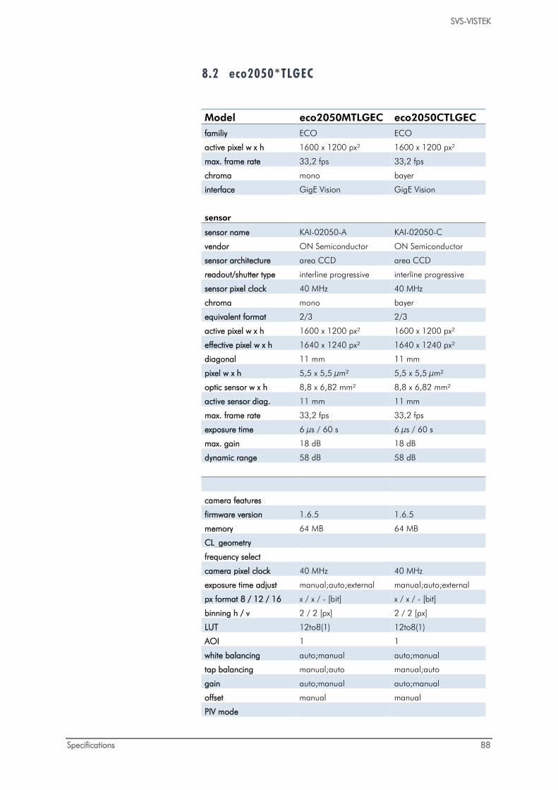
SVS-VISTEK
Specifications 88
8.2 eco2050*TLGEC
Model eco2050MTLGEC eco2050CTLGEC familiy ECO ECO
active pixel w x h 1600 x 1200 px² 1600 x 1200 px²
max. frame rate 33,2 fps 33,2 fps
chroma mono bayer
interface GigE Vision GigE Vision
sensor
sensor name KAI-02050-A KAI-02050-C
vendor ON Semiconductor ON Semiconductor
sensor architecture area CCD area CCD
readout/shutter type interline progressive interline progressive
sensor pixel clock 40 MHz 40 MHz
chroma mono bayer
equivalent format 2/3 2/3
active pixel w x h 1600 x 1200 px² 1600 x 1200 px²
effective pixel w x h 1640 x 1240 px² 1640 x 1240 px²
diagonal 11 mm 11 mm
pixel w x h 5,5 x 5,5 µm² 5,5 x 5,5 µm²
optic sensor w x h 8,8 x 6,82 mm² 8,8 x 6,82 mm²
active sensor diag. 11 mm 11 mm
max. frame rate 33,2 fps 33,2 fps
exposure time 6 µs / 60 s 6 µs / 60 s
max. gain 18 dB 18 dB
dynamic range 58 dB 58 dB
camera features
firmware version 1.6.5 1.6.5
memory 64 MB 64 MB
CL_geometry
frequency select
camera pixel clock 40 MHz 40 MHz
exposure time adjust manual;auto;external manual;auto;external
px format 8 / 12 / 16 x / x / - [bit] x / x / - [bit]
binning h / v 2 / 2 [px] 2 / 2 [px]
LUT 12to8(1) 12to8(1)
AOI 1 1
white balancing auto;manual auto;manual
tap balancing manual;auto manual;auto
gain auto;manual auto;manual
offset manual manual
PIV mode
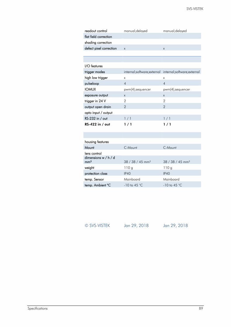
SVS-VISTEK
Specifications 89
readout control manual;delayed manual;delayed
flat field correction
shading correction
defect pixel correction x x
I/O features
trigger modes internal;software;external internal;software;external
high low trigger x x
pulseloop 4 4
IOMUX pwm(4);sequencer pwm(4);sequencer
exposure output x x
trigger in 24 V 2 2
output open drain 2 2
opto input / output
RS-232 in / out 1 / 1 1 / 1
RS-422 in / out 1 / 1 1 / 1
housing features
Mount C-Mount C-Mount
lens control dimensions w / h / d mm³ 38 / 38 / 45 mm³ 38 / 38 / 45 mm³
weight 110 g 110 g
protection class IP40 IP40
temp. Sensor Mainboard Mainboard
temp. Ambient °C -10 to 45 °C -10 to 45 °C
© SVS-VISTEK Jan 29, 2018 Jan 29, 2018
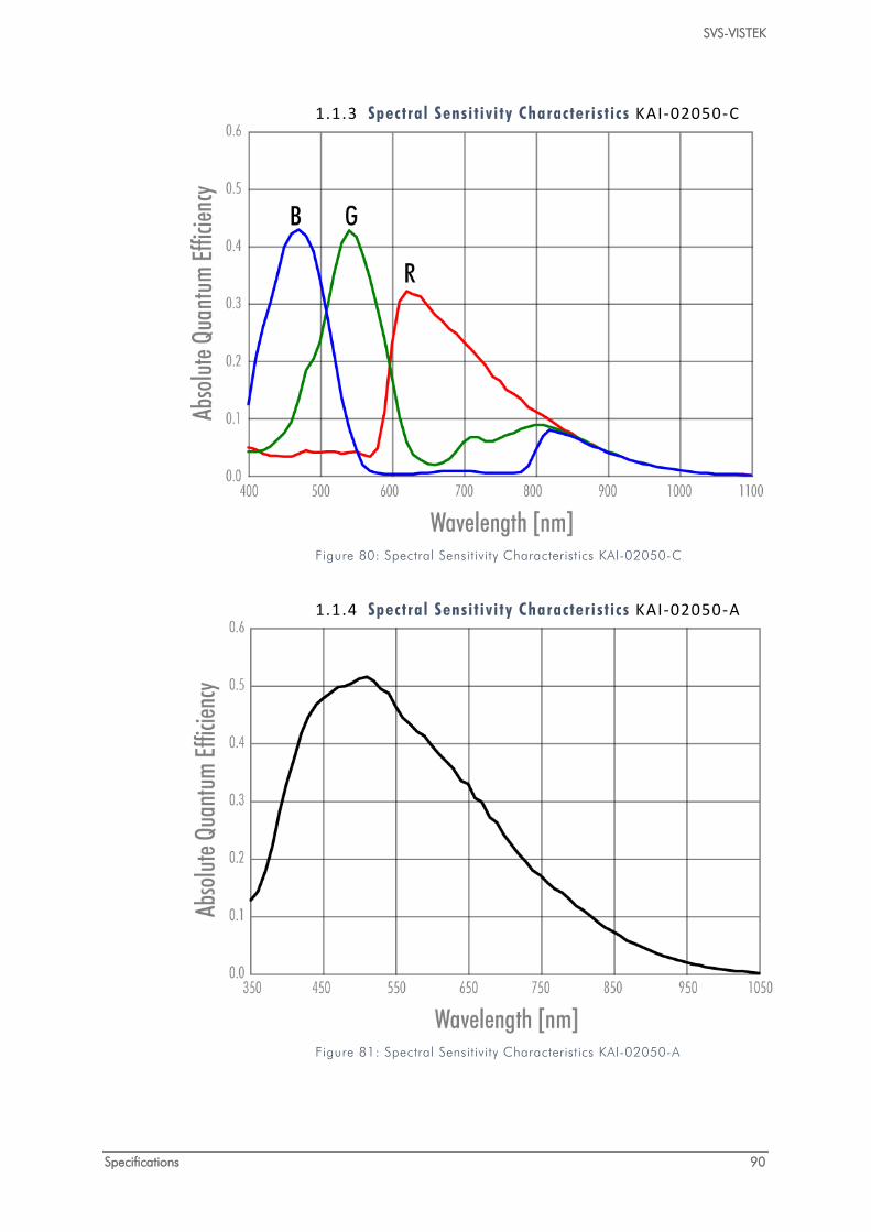
SVS-VISTEK
Specifications 90
1.1.3 Spectral Sensit ivi ty Characteri st ics KAI-02050-C
Figure 80: Spectral Sensitivity Characteristics KAI-02050-C
1.1.4 Spectral Sensit ivi ty Characteri st ics KAI-02050-A
Figure 81: Spectral Sensitivity Characteristics KAI-02050-A

SVS-VISTEK
Specifications 91
8.3 eco2150*TLGEC
Model eco2150MTLGEC eco2150CTLGEC familiy ECO ECO
active pixel w x h 1920 x 1080 px² 1920 x 1080 px²
max. frame rate 31,7 fps 31,7 fps
chroma mono bayer
interface GigE Vision GigE Vision
sensor
sensor name KAI-02150-A KAI-02150-C
vendor ON Semiconductor ON Semiconductor
sensor architecture area CCD area CCD
readout/shutter type interline progressive interline progressive
sensor pixel clock 40 MHz 40 MHz
chroma mono bayer
equivalent format 2/3 2/3
active pixel w x h 1920 x 1080 px² 1920 x 1080 px²
effective pixel w x h 1960 x 1120 px² 1960 x 1120 px²
diagonal 12,1 mm 12,1 mm
pixel w x h 5,5 x 5,5 µm² 5,5 x 5,5 µm²
optic sensor w x h 10,5 x 6,16 mm² 10,5 x 6,16 mm²
active sensor diag. 12,1 mm 12,1 mm
max. frame rate 31,7 fps 31,7 fps
exposure time 6 µs / 60 s 6 µs / 60 s
max. gain 18 dB 18 dB
dynamic range 58 dB 58 dB
camera features
firmware version 1.6.5 1.6.5
memory 64 MB 64 MB
CL_geometry
frequency select
camera pixel clock 40 MHz 40 MHz
exposure time adjust manual;auto;external manual;auto;external
px format 8 / 12 / 16 x / x / - [bit] x / x / - [bit]
binning h / v 2 / 2 [px] 2 / 2 [px]
LUT 12to8(1) 12to8(1)
AOI 1 1
white balancing auto;manual auto;manual
tap balancing manual;auto manual;auto
gain auto;manual auto;manual
offset manual manual
PIV mode

SVS-VISTEK
Specifications 92
readout control manual;delayed manual;delayed
flat field correction
shading correction
defect pixel correction x x
I/O features
trigger modes internal;software;external internal;software;external
high low trigger x x
pulseloop 4 4
IOMUX pwm(4);sequencer pwm(4);sequencer
exposure output x x
trigger in 24 V 2 2
output open drain 2 2
opto input / output
RS-232 in / out 1 / 1 1 / 1
RS-422 in / out 1 / 1 1 / 1
housing features
Mount C-Mount C-Mount
lens control dimensions w / h / d mm³ 38 / 38 / 45 mm³ 38 / 38 / 45 mm³
weight 110 g 110 g
protection class IP40 IP40
temp. Sensor Mainboard Mainboard
temp. Ambient °C -10 to 45 °C -10 to 45 °C
© SVS-VISTEK Jan 29, 2018 Jan 29, 2018
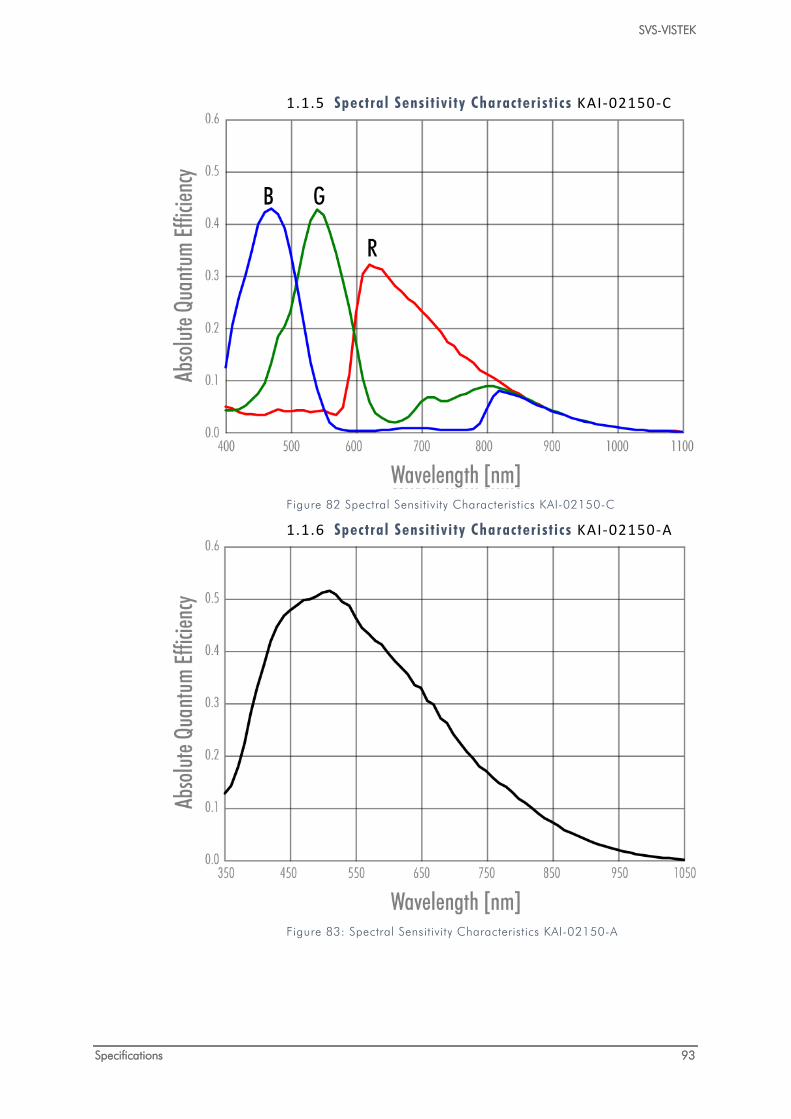
SVS-VISTEK
Specifications 93
1.1.5 Spectral Sensit ivi ty Characteri st ics KAI-02150-C
Figure 82 Spectral Sensitivity Characteristics KAI-02150-C
1.1.6 Spectral Sensit ivi ty Characteri st ics KAI-02150-A
Figure 83: Spectral Sensitivity Characteristics KAI-02150-A
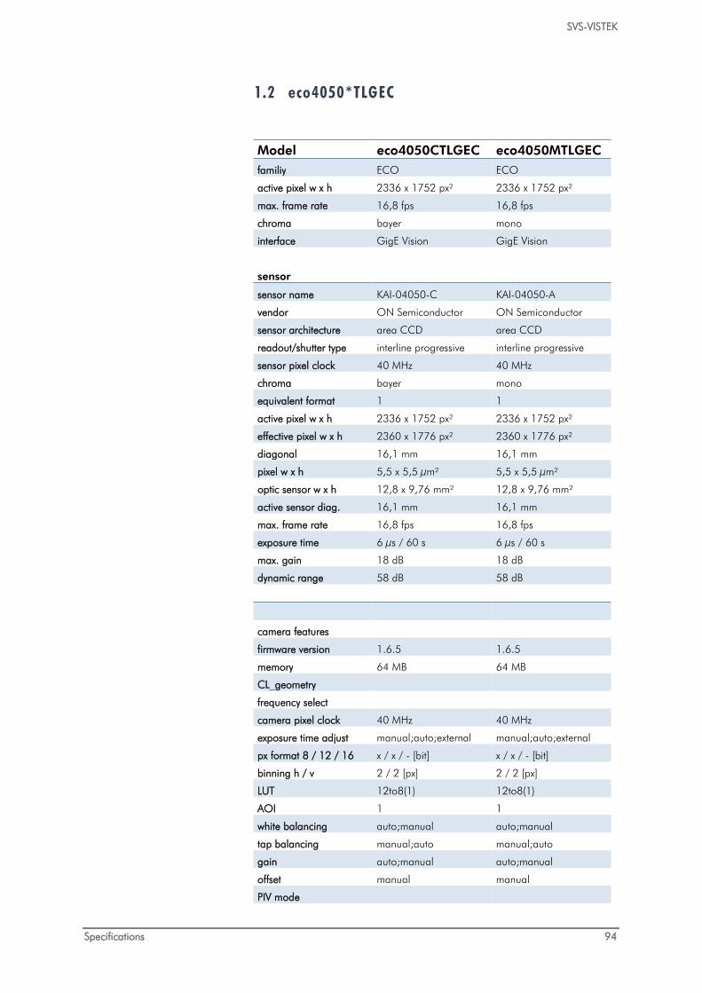
SVS-VISTEK
Specifications 94
1.2 eco4050*TLGEC
Model eco4050CTLGEC eco4050MTLGEC familiy ECO ECO
active pixel w x h 2336 x 1752 px² 2336 x 1752 px²
max. frame rate 16,8 fps 16,8 fps
chroma bayer mono
interface GigE Vision GigE Vision
sensor
sensor name KAI-04050-C KAI-04050-A
vendor ON Semiconductor ON Semiconductor
sensor architecture area CCD area CCD
readout/shutter type interline progressive interline progressive
sensor pixel clock 40 MHz 40 MHz
chroma bayer mono
equivalent format 1 1
active pixel w x h 2336 x 1752 px² 2336 x 1752 px²
effective pixel w x h 2360 x 1776 px² 2360 x 1776 px²
diagonal 16,1 mm 16,1 mm
pixel w x h 5,5 x 5,5 µm² 5,5 x 5,5 µm²
optic sensor w x h 12,8 x 9,76 mm² 12,8 x 9,76 mm²
active sensor diag. 16,1 mm 16,1 mm
max. frame rate 16,8 fps 16,8 fps
exposure time 6 µs / 60 s 6 µs / 60 s
max. gain 18 dB 18 dB
dynamic range 58 dB 58 dB
camera features
firmware version 1.6.5 1.6.5
memory 64 MB 64 MB
CL_geometry
frequency select
camera pixel clock 40 MHz 40 MHz
exposure time adjust manual;auto;external manual;auto;external
px format 8 / 12 / 16 x / x / - [bit] x / x / - [bit]
binning h / v 2 / 2 [px] 2 / 2 [px]
LUT 12to8(1) 12to8(1)
AOI 1 1
white balancing auto;manual auto;manual
tap balancing manual;auto manual;auto
gain auto;manual auto;manual
offset manual manual
PIV mode

SVS-VISTEK
Specifications 95
readout control manual;delayed manual;delayed
flat field correction
shading correction
defect pixel correction x x
I/O features
trigger modes internal;software;external internal;software;external
high low trigger x x
pulseloop 4 4
IOMUX pwm(4);sequencer pwm(4);sequencer
exposure output x x
trigger in 24 V 2 2
output open drain 2 2
opto input / output
RS-232 in / out 1 / 1 1 / 1
RS-422 in / out 1 / 1 1 / 1
housing features
Mount C-Mount C-Mount
lens control dimensions w / h / d mm³ 38 / 38 / 45 mm³ 38 / 38 / 45 mm³
weight 110 g 110 g
protection class IP40 IP40
temp. Sensor Mainboard Mainboard
temp. Ambient °C -10 to 45 °C -10 to 45 °C
© SVS-VISTEK Jan 29, 2018 Jan 29, 2018
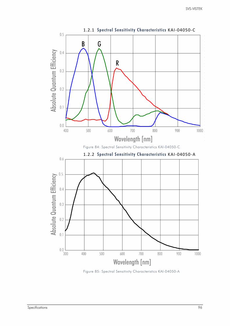
SVS-VISTEK
Specifications 96
1.2.1 Spectral Sensit ivi ty Characteri st ics KAI-04050-C
Figure 84: Spectral Sensitivity Characteristics KAI-04050-C
1.2.2 Spectral Sensit ivi ty Characteri st ics KAI-04050-A
Figure 85: Spectral Sensitivity Characteristics KAI-04050-A
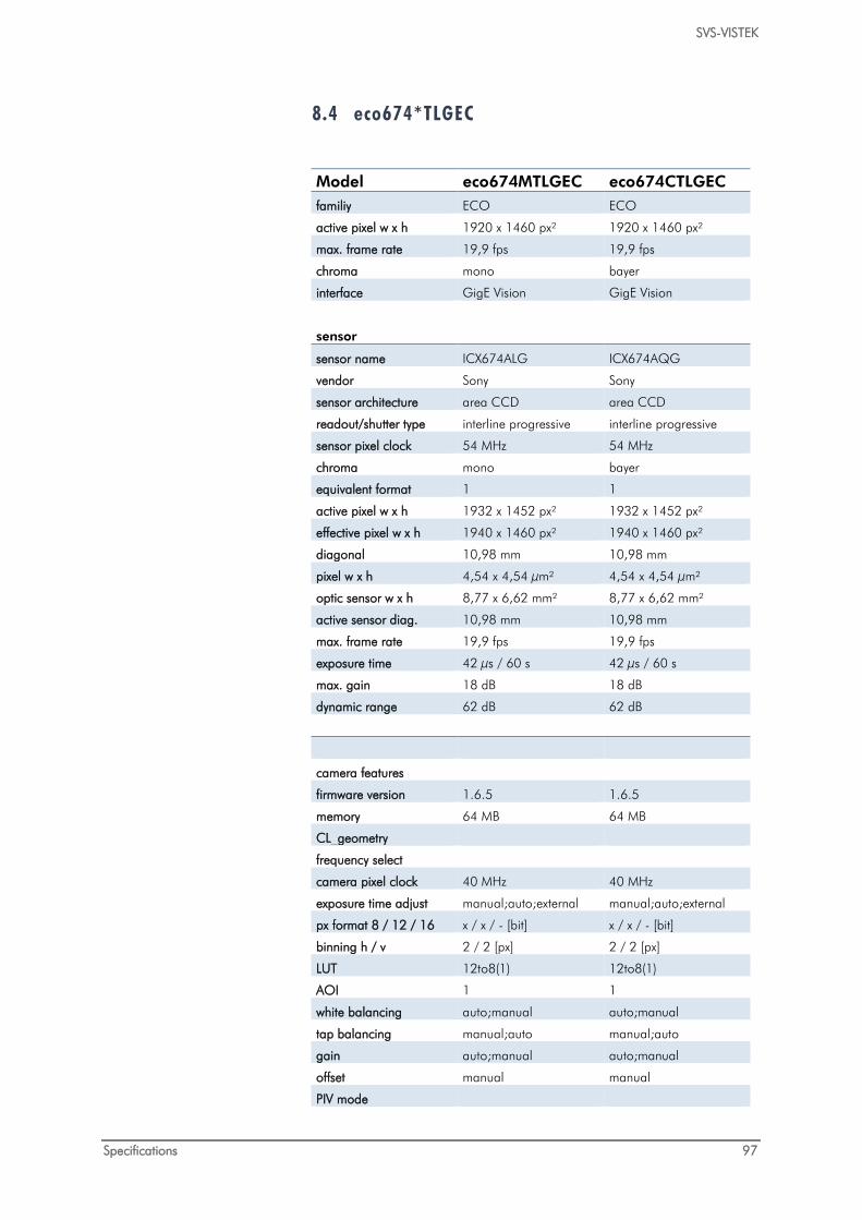
SVS-VISTEK
Specifications 97
8.4 eco674*TLGEC
Model eco674MTLGEC eco674CTLGEC familiy ECO ECO
active pixel w x h 1920 x 1460 px² 1920 x 1460 px²
max. frame rate 19,9 fps 19,9 fps
chroma mono bayer
interface GigE Vision GigE Vision
sensor
sensor name ICX674ALG ICX674AQG
vendor Sony Sony
sensor architecture area CCD area CCD
readout/shutter type interline progressive interline progressive
sensor pixel clock 54 MHz 54 MHz
chroma mono bayer
equivalent format 1 1
active pixel w x h 1932 x 1452 px² 1932 x 1452 px²
effective pixel w x h 1940 x 1460 px² 1940 x 1460 px²
diagonal 10,98 mm 10,98 mm
pixel w x h 4,54 x 4,54 µm² 4,54 x 4,54 µm²
optic sensor w x h 8,77 x 6,62 mm² 8,77 x 6,62 mm²
active sensor diag. 10,98 mm 10,98 mm
max. frame rate 19,9 fps 19,9 fps
exposure time 42 µs / 60 s 42 µs / 60 s
max. gain 18 dB 18 dB
dynamic range 62 dB 62 dB
camera features
firmware version 1.6.5 1.6.5
memory 64 MB 64 MB
CL_geometry
frequency select
camera pixel clock 40 MHz 40 MHz
exposure time adjust manual;auto;external manual;auto;external
px format 8 / 12 / 16 x / x / - [bit] x / x / - [bit]
binning h / v 2 / 2 [px] 2 / 2 [px]
LUT 12to8(1) 12to8(1)
AOI 1 1
white balancing auto;manual auto;manual
tap balancing manual;auto manual;auto
gain auto;manual auto;manual
offset manual manual
PIV mode

SVS-VISTEK
Specifications 98
readout control manual;delayed manual;delayed
flat field correction
shading correction
defect pixel correction x x
I/O features
trigger modes internal;software;external internal;software;external
high low trigger x x
pulseloop 4 4
IOMUX pwm(4);sequencer pwm(4);sequencer
exposure output x x
trigger in 24 V 2 2
output open drain 2 2
opto input / output
RS-232 in / out 1 / 1 1 / 1
RS-422 in / out 1 / 1 1 / 1
housing features
Mount C-Mount C-Mount
lens control dimensions w / h / d mm³ 38 / 38 / 45 mm³ 38 / 38 / 45 mm³
weight 110 g 110 g
protection class IP40 IP40
temp. Sensor Mainboard Mainboard
temp. Ambient °C -10 to 45 °C -10 to 45 °C
© SVS-VISTEK Jan 29, 2018 Jan 29, 2018
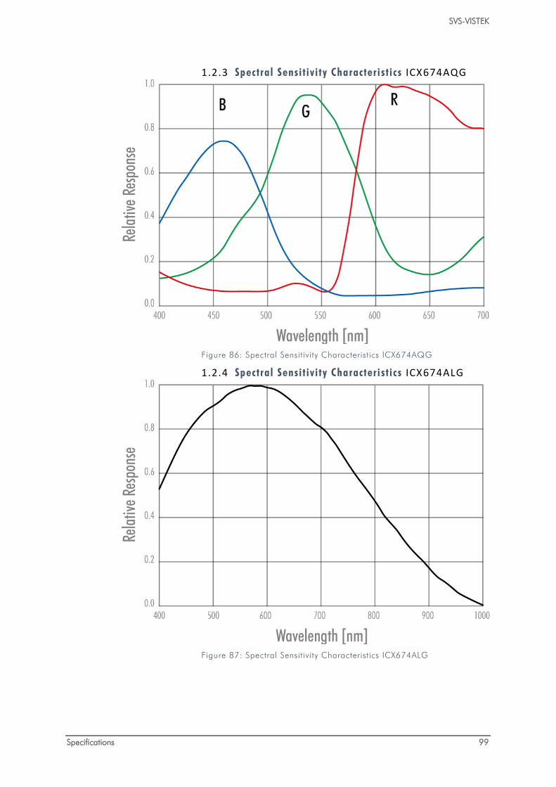
SVS-VISTEK
Specifications 99
1.2.3 Spectral Sensit ivi ty Characteri st ics ICX674AQG
Figure 86: Spectral Sensitivity Characteristics ICX674AQG
1.2.4 Spectral Sensit ivi ty Characteri st ics ICX674ALG
Figure 87: Spectral Sensitivity Characteristics ICX674ALG

SVS-VISTEK
Specifications 100
8.5 eco694*TLGEC
Model eco694MTLGEC eco694CTLGEC familiy ECO ECO
active pixel w x h 2752 x 2204 px² 2752 x 2204 px²
max. frame rate 10,1 fps 10,1 fps
chroma mono bayer
interface GigE Vision GigE Vision
sensor
sensor name ICX694ALG ICX694AQG
vendor Sony Sony
sensor architecture area CCD area CCD
readout/shutter type interline progressive interline progressive
sensor pixel clock 54 MHz 54 MHz
chroma mono bayer
equivalent format 1 1
active pixel w x h 2750 x 2200 px² 2750 x 2200 px²
effective pixel w x h 2758 x 2208 px² 2758 x 2208 px²
diagonal 15,99 mm 15,99 mm
pixel w x h 4,54 x 4,54 µm² 4,54 x 4,54 µm²
optic sensor w x h 12,4 x 10,0 mm² 12,4 x 10,0 mm²
active sensor diag. 15,99 mm 15,99 mm
max. frame rate 10,1 fps 10,1 fps
exposure time 42 µs / 60 s 42 µs / 60 s
max. gain 18 dB 18 dB
dynamic range 58 dB 58 dB
camera features
firmware version 1.6.5 1.6.5
memory 64 MB 64 MB
CL_geometry
frequency select
camera pixel clock 40 MHz 40 MHz
exposure time adjust manual;auto;external manual;auto;external
px format 8 / 12 / 16 x / x / - [bit] x / x / - [bit]
binning h / v 2 / 2 [px] 2 / 2 [px]
LUT 12to8(1) 12to8(1)
AOI 1 1
white balancing auto;manual auto;manual
tap balancing manual;auto manual;auto
gain auto;manual auto;manual
offset manual manual
PIV mode

SVS-VISTEK
Specifications 101
readout control manual;delayed manual;delayed
flat field correction
shading correction
defect pixel correction x x
I/O features
trigger modes internal;software;external internal;software;external
high low trigger x x
pulseloop 4 4
IOMUX pwm(4);sequencer pwm(4);sequencer
exposure output x x
trigger in 24 V 2 2
output open drain 2 2
opto input / output
RS-232 in / out 1 / 1 1 / 1
RS-422 in / out 1 / 1 1 / 1
housing features
Mount C-Mount C-Mount
lens control dimensions w / h / d mm³ 38 / 38 / 45 mm³ 38 / 38 / 45 mm³
weight 110 g 110 g
protection class IP40 IP40
temp. Sensor Mainboard Mainboard
temp. Ambient °C -10 to 45 °C -10 to 45 °C
© SVS-VISTEK Jan 29, 2018 Jan 29, 2018
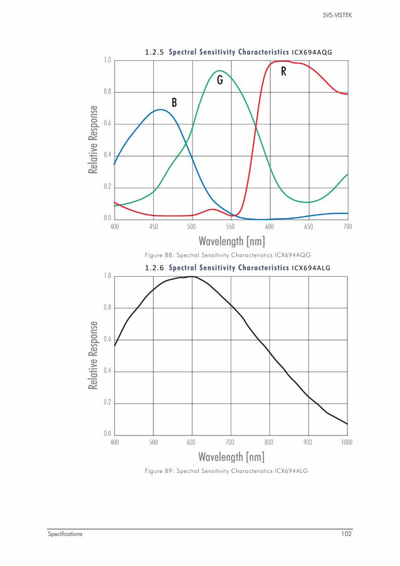
SVS-VISTEK
Specifications 102
1.2.5 Spectral Sensit ivi ty Characteri st ics ICX694AQG
Figure 88: Spectral Sensitivity Characteristics ICX694AQG
1.2.6 Spectral Sensit ivi ty Characteri st ics ICX694ALG
Figure 89: Spectral Sensitivity Characteristics ICX694ALG

SVS-VISTEK
Specifications 103
8.6 eco695*TLGEC
Model eco695CTLGEC eco695MTLGEC familiy ECO ECO
active pixel w x h 2752 x 2204 px² 2752 x 2204 px²
max. frame rate 10,1 fps 10,1 fps
chroma bayer mono
interface GigE Vision GigE Vision
sensor
sensor name ICX695AQG ICX695ALG
vendor Sony Sony
sensor architecture area CCD area CCD
readout/shutter type interline progressive interline progressive
sensor pixel clock 54 MHz 54 MHz
chroma bayer mono
equivalent format 1 1
active pixel w x h 2750 x 2200 px² 2750 x 2200 px²
effective pixel w x h 2758 x 2208 px² 2758 x 2208 px²
diagonal 15,99 mm 15,99 mm
pixel w x h 4,54 x 4,54 µm² 4,54 x 4,54 µm²
optic sensor w x h 12,4 x 10,0 mm² 12,4 x 10,0 mm²
active sensor diag. 15,99 mm 15,99 mm
max. frame rate 10,1 fps 10,1 fps
exposure time 42 µs / 60 s 42 µs / 60 s
max. gain 18 dB 18 dB
dynamic range 58 dB 58 dB
camera features
firmware version 1.6.5 1.6.5
memory 64 MB 64 MB
CL_geometry
frequency select
camera pixel clock 40 MHz 40 MHz
exposure time adjust manual;auto;external manual;auto;external
px format 8 / 12 / 16 x / x / - [bit] x / x / - [bit]
binning h / v 2 / 2 [px] 2 / 2 [px]
LUT 12to8(1) 12to8(1)
AOI 1 1
white balancing auto;manual auto;manual
tap balancing manual;auto manual;auto
gain auto;manual auto;manual
offset manual manual
PIV mode

SVS-VISTEK
Specifications 104
readout control manual;delayed manual;delayed
flat field correction
shading correction
defect pixel correction x x
I/O features
trigger modes internal;software;external internal;software;external
high low trigger x x
pulseloop 4 4
IOMUX pwm(4);sequencer pwm(4);sequencer
exposure output x x
trigger in 24 V 2 2
output open drain 2 2
opto input / output
RS-232 in / out 1 / 1 1 / 1
RS-422 in / out 1 / 1 1 / 1
housing features
Mount C-Mount C-Mount
lens control dimensions w / h / d mm³ 38 / 38 / 45 mm³ 38 / 38 / 45 mm³
weight 110 g 110 g
protection class IP40 IP40
temp. Sensor Mainboard Mainboard
temp. Ambient °C -10 to 45 °C -10 to 45 °C
© SVS-VISTEK Jan 29, 2018 Jan 29, 2018
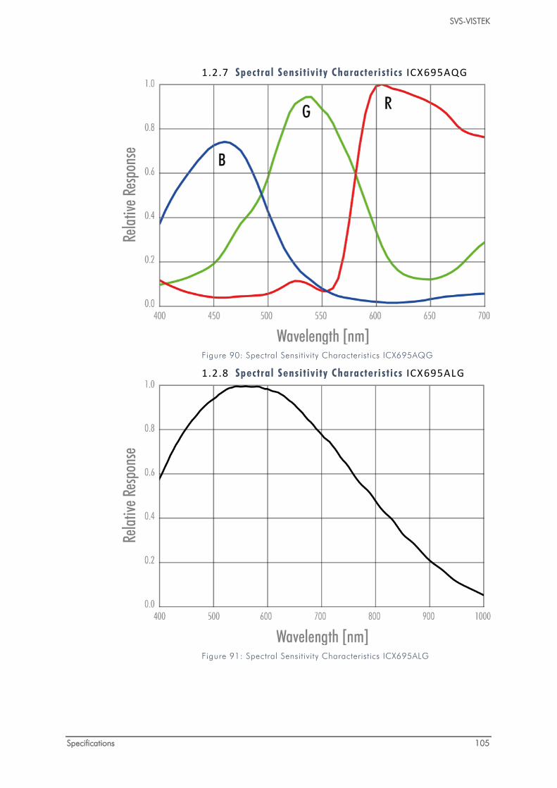
SVS-VISTEK
Specifications 105
1.2.7 Spectral Sensit ivi ty Characteri st ics ICX695AQG
Figure 90: Spectral Sensitivity Characteristics ICX695AQG
1.2.8 Spectral Sensit ivi ty Characteri st ics ICX695ALG
Figure 91: Spectral Sensitivity Characteristics ICX695ALG

SVS-VISTEK
Specifications 106
8.7 eco814*TLGEC
Model eco814CTLGEC eco814MTLGEC familiy ECO ECO
active pixel w x h 3360 x 2712 px² 3360 x 2712 px²
max. frame rate 7 fps 7 fps
chroma bayer mono
interface GigE Vision GigE Vision
sensor
sensor name ICX814AQA ICX814ALA
vendor Sony Sony
sensor architecture area CCD area CCD
readout/shutter type interline progressive interline progressive
sensor pixel clock 54 MHz 54 MHz
chroma bayer mono
equivalent format 1 1
active pixel w x h 3380 x 2704 px² 3380 x 2704 px²
effective pixel w x h 3388 x 2712 px² 3388 x 2712 px²
diagonal 15,97 mm 15,97 mm
pixel w x h 3,69 x 3,69 µm² 3,69 x 3,69 µm²
optic sensor w x h 12,4 x 10,0 mm² 12,4 x 10,0 mm²
active sensor diag. 15,97 mm 15,97 mm
max. frame rate 7 fps 7 fps
exposure time 42 µs / 60 s 42 µs / 60 s
max. gain 18 dB 18 dB
dynamic range 60 dB 60 dB
camera features
firmware version 1.6.5 1.6.5
memory 64 MB 64 MB
CL_geometry
frequency select
camera pixel clock 40 MHz 40 MHz
exposure time adjust manual;auto;external manual;auto;external
px format 8 / 12 / 16 x / x / - [bit] x / x / - [bit]
binning h / v 2 / 2 [px] 2 / 2 [px]
LUT 12to8(1) 12to8(1)
AOI 1 1
white balancing auto;manual auto;manual
tap balancing manual;auto manual;auto
gain auto;manual auto;manual
offset manual manual
PIV mode

SVS-VISTEK
Specifications 107
readout control manual;delayed manual;delayed
flat field correction
shading correction
defect pixel correction x x
I/O features
trigger modes internal;software;external internal;software;external
high low trigger x x
pulseloop 4 4
IOMUX pwm(4);sequencer pwm(4);sequencer
exposure output x x
trigger in 24 V 2 2
output open drain 2 2
opto input / output
RS-232 in / out 1 / 1 1 / 1
RS-422 in / out 1 / 1 1 / 1
housing features
Mount C-Mount C-Mount
lens control dimensions w / h / d mm³ 38 / 38 / 45 mm³ 38 / 38 / 45 mm³
weight 110 g 110 g
protection class IP40 IP40
temp. Sensor Mainboard Mainboard
temp. Ambient °C -10 to 45 °C -10 to 45 °C
© SVS-VISTEK Jan 29, 2018 Jan 29, 2018
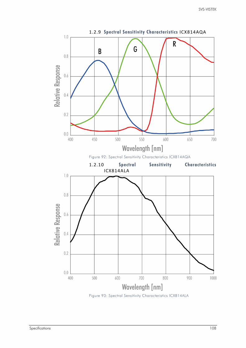
SVS-VISTEK
Specifications 108
1.2.9 Spectral Sensit ivi ty Characteri st ics ICX814AQA
Figure 92: Spectral Sensitivity Characteristics ICX814AQA
1.2.10 Spectral Sensit ivi ty Characteri st ics ICX814ALA
Figure 93: Spectral Sensitivity Characteristics ICX814ALA

SVS-VISTEK
Specifications 109
8.8 eco815CTLGEC
Model eco815CTLGEC eco815MTLGEC familiy ECO ECO
active pixel w x h 3360 x 2712 px² 3360 x 2712 px²
max. frame rate 7 fps 7 fps
chroma bayer mono
interface GigE Vision GigE Vision
sensor
sensor name ICX815AQA ICX815ALA
vendor Sony Sony
sensor architecture area CCD area CCD
readout/shutter type interline progressive interline progressive
sensor pixel clock 54 MHz 54 MHz
chroma bayer mono
equivalent format 1 1
active pixel w x h 3380 x 2704 px² 3380 x 2704 px²
effective pixel w x h 3388 x 2712 px² 3388 x 2712 px²
diagonal 15,97 mm 15,97 mm
pixel w x h 3,69 x 3,69 µm² 3,69 x 3,69 µm²
optic sensor w x h 12,4 x 10,0 mm² 12,4 x 10,0 mm²
active sensor diag. 15,97 mm 15,97 mm
max. frame rate 7 fps 7 fps
exposure time 42 µs / 60 s 42 µs / 60 s
max. gain 18 dB 18 dB
dynamic range 58 dB 58 dB
camera features
firmware version 1.6.5 1.6.5
memory 64 MB 64 MB
CL_geometry
frequency select
camera pixel clock 40 MHz 40 MHz
exposure time adjust manual;auto;external manual;auto;external
px format 8 / 12 / 16 x / x / - [bit] x / x / - [bit]
binning h / v 2 / 2 [px] 2 / 2 [px]
LUT 12to8(1) 12to8(1)
AOI 1 1
white balancing auto;manual auto;manual
tap balancing manual;auto manual;auto
gain auto;manual auto;manual
offset manual manual
PIV mode

SVS-VISTEK
Specifications 110
readout control manual;delayed manual;delayed
flat field correction
shading correction
defect pixel correction x x
I/O features
trigger modes internal;software;external internal;software;external
high low trigger x x
pulseloop 4 4
IOMUX pwm(4);sequencer pwm(4);sequencer
exposure output x x
trigger in 24 V 2 2
output open drain 2 2
opto input / output
RS-232 in / out 1 / 1 1 / 1
RS-422 in / out 1 / 1 1 / 1
housing features
Mount C-Mount C-Mount
lens control dimensions w / h / d mm³ 38 / 38 / 45 mm³ 38 / 38 / 45 mm³
weight 110 g 110 g
protection class IP40 IP40
temp. Sensor Mainboard Mainboard
temp. Ambient °C -10 to 45 °C -10 to 45 °C
© SVS-VISTEK Jan 29, 2018 Jan 29, 2018
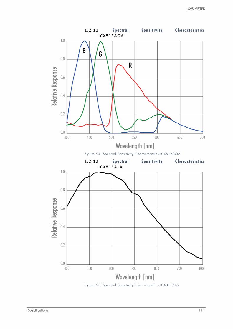
SVS-VISTEK
Specifications 111
1.2.11 Spectral Sensit ivi ty Characteri st ics ICX815AQA
Figure 94: Spectral Sensitivity Characteristics ICX815AQA
1.2.12 Spectral Sensit ivi ty Characteri st ics ICX815ALA
Figure 95: Spectral Sensitivity Characteristics ICX815ALA

SVS-VISTEK
Specifications 112
8.9 eco834*TLGEC
Model eco834MTLGEC eco834CTLGEC familiy ECO ECO
active pixel w x h 4224 x 2838 px² 4224 x 2838 px²
max. frame rate 5,5 fps 5,5 fps
chroma mono bayer
interface GigE Vision GigE Vision
sensor
sensor name ICX834ALG ICX834AQG
vendor Sony Sony
sensor architecture area CCD area CCD
readout/shutter type interline progressive interline progressive
sensor pixel clock 54 MHz 54 MHz
chroma mono bayer
equivalent format 1 1
active pixel w x h 4242 x 2830 px² 4242 x 2830 px²
effective pixel w x h 4250 x 2838 px² 4250 x 2838 px²
diagonal 15,81 mm 15,81 mm
pixel w x h 3,1 x 3,1 µm² 3,1 x 3,1 µm²
optic sensor w x h 13,1 x 8,79 mm² 13,1 x 8,79 mm²
active sensor diag. 15,81 mm 15,81 mm
max. frame rate 5,5 fps 5,5 fps
exposure time 42 µs / 60 s 42 µs / 60 s
max. gain 18 dB 18 dB
dynamic range 55 dB 55 dB
camera features
firmware version 1.6.5 1.6.5
memory 64 MB 64 MB
CL_geometry
frequency select
camera pixel clock 40 MHz 40 MHz
exposure time adjust manual;auto;external manual;auto;external
px format 8 / 12 / 16 x / x / - [bit] x / x / - [bit]
binning h / v 2 / 2 [px] 2 / 2 [px]
LUT 12to8(1) 12to8(1)
AOI 1 1
white balancing auto;manual auto;manual
tap balancing manual;auto manual;auto
gain auto;manual auto;manual
offset manual manual
PIV mode

SVS-VISTEK
Specifications 113
readout control manual;delayed manual;delayed
flat field correction
shading correction
defect pixel correction x x
I/O features
trigger modes internal;software;external internal;software;external
high low trigger x x
pulseloop 4 4
IOMUX pwm(4);sequencer pwm(4);sequencer
exposure output x x
trigger in 24 V 2 2
output open drain 2 2
opto input / output
RS-232 in / out 1 / 1 1 / 1
RS-422 in / out 1 / 1 1 / 1
housing features
Mount C-Mount C-Mount
lens control dimensions w / h / d mm³ 38 / 38 / 45 mm³ 38 / 38 / 45 mm³
weight 110 g 110 g
protection class IP40 IP40
temp. Sensor Mainboard Mainboard
temp. Ambient °C -10 to 45 °C -10 to 45 °C
© SVS-VISTEK Jan 29, 2018 Jan 29, 2018
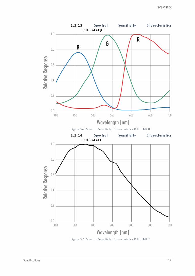
SVS-VISTEK
Specifications 114
1.2.13 Spectral Sensit ivi ty Characteri st ics ICX834AQG
Figure 96: Spectral Sensitivity Characteristics ICX834AQG
1.2.14 Spectral Sensit ivi ty Characteri st ics ICX834ALG
Figure 97: Spectral Sensitivity Characteristics ICX834ALG
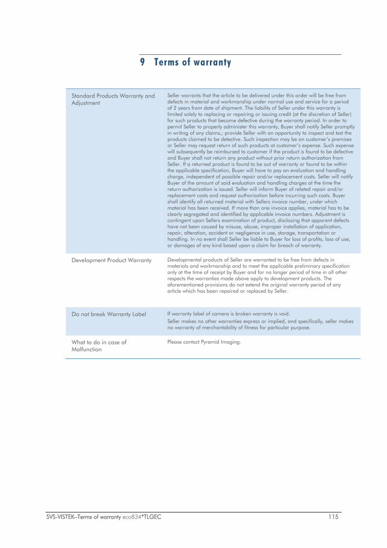
SVS-VISTEK–Terms of warranty eco834*TLGEC 115
9 Terms of warranty
Standard Products Warranty and Adjustment
Seller warrants that the article to be delivered under this order will be free from defects in material and workmanship under normal use and service for a period of 2 years from date of shipment. The liability of Seller under this warranty is limited solely to replacing or repairing or issuing credit (at the discretion of Seller) for such products that become defective during the warranty period. In order to permit Seller to properly administer this warranty, Buyer shall notify Seller promptly in writing of any claims,; provide Seller with an opportunity to inspect and test the products claimed to be detective. Such inspection may be on customer’s premises or Seller may request return of such products at customer’s expense. Such expense will subsequently be reimbursed to customer if the product is found to be defective and Buyer shall not return any product without prior return authorization from Seller. If a returned product is found to be out of warranty or found to be within the applicable specification, Buyer will have to pay an evaluation and handling charge, independent of possible repair and/or replacement costs. Seller will notify Buyer of the amount of said evaluation and handling charges at the time the return authorization is issued. Seller will inform Buyer of related repair and/or replacement costs and request authorization before incurring such costs. Buyer shall identify all returned material with Sellers invoice number, under which material has been received. If more than one invoice applies, material has to be clearly segregated and identified by applicable invoice numbers. Adjustment is contingent upon Sellers examination of product, disclosing that apparent defects have not been caused by misuse, abuse, improper installation of application, repair, alteration, accident or negligence in use, storage, transportation or handling. In no event shall Seller be liable to Buyer for loss of profits, loss of use, or damages of any kind based upon a claim for breach of warranty.
Development Product Warranty Developmental products of Seller are warranted to be free from defects in materials and workmanship and to meet the applicable preliminary specification only at the time of receipt by Buyer and for no longer period of time in all other respects the warranties made above apply to development products. The aforementioned provisions do not extend the original warranty period of any article which has been repaired or replaced by Seller.
Do not break Warranty Label If warranty label of camera is broken warranty is void. Seller makes no other warranties express or implied, and specifically, seller makes no warranty of merchantability of fitness for particular purpose.
What to do in case of Malfunction
Please contact Pyramid Imaging.

SVS-VISTEK
Terms of warranty 116
SVS-VISTEK–Troubleshooting FAQ 117
10 Troubleshooting 10.1 FAQ
Problem Solution
Camera does not respond to light. Check if camera is set to “Mode 0“. I.e. free running with programmed exposure ctrl. When done, check with the program “Convenient Cam“ if you can read back any data from the camera, such as “Mode“, “type“ of CCD, exposure time settings, etc.. If “Mode 0“ works properly, check the signals of the camera in the desired operation mode like “Mode 1“ or “Mode 2“. In these modes, check if the ExSync signal is present. Please note that a TTL signal must be fed to the trigger connector if it is not provided by the frame grabber (LVDS type). The typical signal swing must be around 5 V. Lower levels will not be detected by the camera... If you use a TTL level signal fed to the “TB 5 connector“ check the quality and swing. If these signals are not present or don’t have the proper quality, the camera cannot read out any frame (Mode 1 and 2). Beware of spikes on the signal.
Image is present but distorted. Check the camera configuration file of your frame grabber. Check number of “front- and back porch“ pixel. Wrong numbers in configuration file can cause sync problems. Check if your frame grabber can work with the data rate of the camera.
Image of a color version camera looks strange or false colors appear.
If the raw image looks OK, check the camera file to see if the pixels need to be shifted by either one pixel or one line. The image depends on the algorithm used. If the algorithm is starting with the wrong pixel such effects appear.
Colors rendition of a color versions not as expected – especially when using halogen light.
Halogen light contains strong portions of IR radiation. Use cut-off filters at around 730 nm like “Schott KG 3“ to prevent IR radiation reaching the CCD.
No serial communication is possible between the camera and the PC.
Use “load camera DLL” and try again.

SVS-VISTEK
Troubleshooting 118
10.2 Support Request Form / Check List Dear valued customer,
In order to help you with your camera and any interfacing problems we request that you fill in a description of your problems when you use the camera. Please fax or email this form to Pyramid Imaging.
Operating System (E.g. Win 7, XP):
Which Camera are you using? Type (e.g.: svs3625MTHCPC):
Serial Number:
Which Accessories are you using? Power Supply:
Cable:
Lens Type and Focal Length:
Firmware No. of Version:
Operation Mode:
Please send a screenshot of “ConvCam” screen or log file.
In case of EURESYS Grabber:
Brand and Type:
Driver Version:
If Patch please specify:
Camera file used:
Short Description of Problem (E.g. missing lines, noisy image, missing bits etc.):
Please fax this form to +1 (866) 874-9521.
SENDE R:
FIRM:
TEL:
M AIL:

SVS-VISTEK
Troubleshooting 119
Space for further descr ipt ions, screenshots and log-fi les
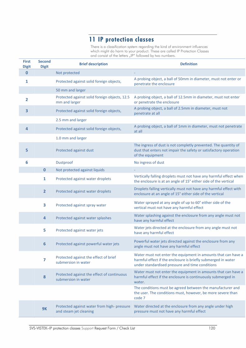
SVS-VISTEK–IP protection classes Support Request Form / Check List 120
11 IP protection classes There is a classification system regarding the kind of environment influences which might do harm to your product. These are called IP Protection Classes and consist of the letters „IP“ followed by two numbers.
First Digit
Second Digit Brief description Definition
0
Not protected -
1
Protected against solid foreign objects, A probing object, a ball of 50mm in diameter, must not enter or penetrate the enclosure
50 mm and larger
2
Protected against solid foreign objects, 12.5 mm and larger
A probing object, a ball of 12.5mm in diameter, must not enter or penetrate the enclosure
3
Protected against solid foreign objects, A probing object, a ball of 2.5mm in diameter, must not penetrate at all
2.5 mm and larger 4
Protected against solid foreign objects, A probing object, a ball of 1mm in diameter, must not penetrate at all
1.0 mm and larger
5
Protected against dust The ingress of dust is not completly prevented. The quantity of dust that enters not impair the safety or satisfactory operation of the equipment
6
Dustproof No ingress of dust
0 Not protected against liquids -
1 Protected against water droplets Vertically falling droplets must not have any harmful effect when the enclosure is at an angle of 15° either side of the vertical
2 Protected against water droplets Droplets falling vertically must not have any harmful effect with enclosure at an angle of 15° either side of the vertical
3 Protected against spray water Water sprayed at any angle of up to 60° either side of the vertical must not have any harmful effect
4 Protected against water splashes Water splashing against the enclosure from any angle must not have any harmful effect
5 Protected against water jets Water jets directed at the enclosure from any angle must not have any harmful effect
6 Protected against powerful water jets Powerful water jets directed against the enclosure from any angle must not have any harmful effect
7 Protected against the effect of brief submersion in water
Water must not enter the equipment in amounts that can have a harmful effect if the enclosure is briefly submerged in water under standardised pressure and time conditions
8 Protected against the effect of continuous submersion in water
Water must not enter the equipment in amounts that can have a harmful effect if the enclosure is continuously submerged in water.
The conditions must be agreed between the manufacturer and the user. The conditions must, however, be more severe than code 7
9K Protected against water from high- pressure and steam jet cleaning
Water directed at the enclosure from any angle under high pressure must not have any harmful effect

SVS-VISTEK
IP protection classes 121
SVS-VISTEK–Glossary of Terms Support Request Form / Check List 122
12 Glossary of Terms Spherical aberration occurs when light rays enter near the edge of the lens; Chromatic aberration is caused by different refractive indexes of different wavelengths of the light. (Blue is more refractive than red)
Analogue-to-Digital Converter, also known as A/D converter
In optics, Aperture defines a hole or an opening through which light travels. In optical system the Aperture determines the cone angle of a bundle of rays that come to a focus in the image plane. The Aperture can be limited by an iris, but it is not solely reliant on the iris. The diameter of the lens has a larger influence on the capability of the optical system.
A Bayer filter mosaic or pattern is a color filter array (CFA) deposited onto the surface of a CCD or CMOS sensor for capturing RGB color images. The filter mosaic has a defied sequence of red, green and blue pixels such that the captured image can be transported as a monochrome image to the host (using less bandwidth); where after the RGB information is recombined in a computer algorithm.
Binning combines the charge from two (or more) pixels to achieve higher dynamics while sacrifying resolution.
Bit-depth is the number of digital bits available at the output of the Analog-to-Digital Converter (ADC) indicating the distribution of the darkest to the brightest value of a single pixel.
Camera Link is a multiple-pair serial communication protocol standard [1] designed for computer vision applications based on the National Semiconductor interface Channel-link. It was designed for the purpose of standardizing scientific and industrial video products including cameras, cables and frame grabbers.
Charge Coupled Device. Commonly used technology used for camera sensors used to detect & quantify light, i.e. for capturing images in an electronic manner. CCDs were first introduced in the early 70ies.
Complementary Metal–Oxide–Semiconductor. A more recently adopted technology used for camera sensors with in-pixel amplifiers used to detect & quantify light, i.e. capturing images in an electronic manner.
Central Processing Unit of a computer. Also referred to as the processor chip.
Decibel (dB) is a logarithmic unit used to express the ratio between two values of a physical quantity.
For reducing width or height of an image, decimation can be used (CMOS sensors only). Columns or rows can be ignored. Image readout time is thereby reduced. Identifies the location of defect pixels unique for every sensor. A factory generated defect map is delivered and implemented with each camera.
Erasable Programmable Read Only Memory is a type of memory chip that retains its data when its power supply is switched off.
Erasable Programmable Read Only Memory is a type of memory chip that retains its data when its power supply is switched off.
or programmed exposure time. Frames are read out continuously.
In electronics, gain is a measure of the ability of a two-port circuit (often an amplifier) to increase the power or amplitude of a signal from the input to the output port by adding energy to the signal.
Aberration
ADC Aperture
Bayer Pattern
Binning
Bit-Depth
Camera Link
CCD
CMOS
CPU
dB
Decimation
Defect map
EPROM
External Trigger
fixed frequency Gain
SVS-VISTEK
Glossary of Terms 123
Gamma correction is a nonlinear operation used to code and decode luminance values in video or still image systems.
Provides a generic programming interface for all kinds of cameras and devices. Regardless what interface technology is used (GigE Vision, USB3 Vision, CoaXPress, Camera Link, etc.) or which features are implemented, the application programming interface (API) will always be the same.
GigE Vision is an interface standard introduced in 2006 for high-performance industrial cameras. It provides a framework for transmitting high-speed video and related control data over Gigabit Ethernet networks.
Graphics Processing Unit of a computer.
Cable connectors commonly used for power, triggers, I/Os and strobe lights
see Gain.
In computer networking, jumbo frames are Ethernet frames with more than 1500 bytes of payload. Conventionally, jumbo frames can carry up to 9000 bytes of payload. Some Gigabit Ethernet switches and Gigabit Ethernet network interface cards do not support jumbo frames.
Mechanical interface/connection for attaching lenses to the camera.
Multicast (one-to-many or many-to-many distribution) is an ethernet group communication where information is addressed to a group of destination computers simultaneously. Multicast should not be confused with physical layer point-to-multipoint communication.
Pulse width modulation. Keeping voltage at the same level while limiting current flow by switching on an off at a very high frequency.
A method for reading out fewer lines from the sensor, but “skipping” lines above and below the desired area. Typically applied to CCD sensors. In most CMOS image sensors an AOI (area of interest) or ROI (region of interest) can be defined by selecting the area to be read. This leads to increased frame rate.
The base clock (beat) that operates the sensor chip is. It is typically also the clock with which pixels are presented at the output node of the image sensor.
A camera RAW image file contains minimally processed data from the image sensor. It is referred as raw in its meaning. SVS-VISTEK plays out RAW only.
Read-Out control defines a delay between exposure and image readout. It allows the user to program a delay value (time) for the readout from the sensor. It is useful for preventing CPU overload when handling very large images or managing several cameras on a limited Ethernet connection. Shading manifests itself a decreasing brightness towards the edges of the image or a brightness variation from one side of the image to the other.
Shading can be caused by non-uniform illumination, non-uniform camera sensitivity, vignetting of the lens, or even dirt and dust on glass surfaces (lens).
An in-camera algorithm for real time correction of shading. It typically permits user configuration. By pointing at a known uniform evenly illuminated surface it allows the microprocessor in the camera to create a correction definition, subsequently applied to the image during readout.
Shutter is a device or technique that allows light to pass for a determined period of time, exposing photographic film or a light-sensitive electronic sensor to light in order to capture a permanent image of a scene.
Gamma
GenICam
GigE Vision
GPU Hirose ISO Jumbo Frames
Mount Multicast
PWM
Partial Scan
Pixel clock
RAW
Read-Out-Control
Shading
Shading correction
Shutter
SVS-VISTEK
Glossary of Terms 124
A bright light source with a very short light pulse. Ideal for use with industrial cameras, e.g. for “freezing” the image capture of fast moving objects. Can often be a substitute for the electronic shutter of the image sensor. Certain industrial cameras have dedicated in-camera output drivers for precisely controlling one or more strobe lights.
CCD sensors can occur divided into two, four or more regions to double/quadruple the read out time.
TCP/IP provides end-to-end connectivity specifying how data should be packetized, addressed, transmitted, routed and received at the destination.
The USB3 Vision interface is based on the standard USB 3.0 interface and uses USB 3.0 ports. Components from different manufacturers will easily communicate with each other.
Cameras for industrial use usually provide a set of different trigger modes with which they can be operated. The most common trigger modes are: (1) Programmable shutter trigger mode. Each image is captured with a pre-defined shutter time; (2) Pulse-Width Control trigger. The image capture is initiated by the leading edge of the trigger pulse and the shutter time is governed by the width of the pulse; (3) Internal trigger or Free-Running mode. The camera captures images at the fastest possible frame rate permitted by the readout time.
Extensible Markup Language (XML) is a markup language that defines a set of rules for encoding documents in a format which is both human-readable and machine-readable
Strobe light
Tap
TCP/IP
USB3 Vision
Trigger modes
XML Files
SVS-VISTEK–Index of figures Support Request Form / Check List 125
13 Index of figures Figure 1: Table of safety messages ...................................................... 6
Figure 1: 4IO concept with up to 4 switching LED lights ...................... 11
Figure 3: Camera status LED codes .................................................. 12
Figure 4: Screenshot of SVCapture 2.x .............................................. 13
Figure 5: searching the camera to be updated ................................... 20
Figure 6: firmware update has just been executed .............................. 20
Figure 7: basic Illustration of driver circuit ......................................... 22
Figure 1: Illustration of RJ45 female connector ................................... 23
FIGURE 9: ILLUSTRATION OF DATA REDUCTION WITH JUMBO FRAMES .... 24
FIGURE 10: ILLUSTRATION OF CONNECTING MULTIPLE CAMERAS ON MULTI NIPS ..................................................................................... 25
FIGURE 11: ILLUSTRATION OF CONNECTING MULTIPLE CAMERAS WITH A SWITCH ........................................................................................... 25
Figure 12: Illustration of a camera casting to multiple receivers (multicast) ...................................................................................................... 26
Figure 13: Illustration of Hirose 12 Pin & pin-out (HR10A-10R-12PB) ... 27
Figure 14: Illustration of C- & CS-Mount differences ........................... 31
Figure 15: Illustration Cross-section of a CCD sensor from Sony ......... 32
Figure 16: Illustration of interline transfer with columns and rows .......... 33
Figure 17: motion blur with global shutter and moving objects ............... 34
Figure 18 rolling shutter with moving objects(geometric distortion) ........ 34
Figure 19: interlaced effect ................................................................ 34
Figure 1: illustration of rising amount of values/gray scales by increasing the bit format .................................................................................. 38
Figure 1: Simplified illustration of a quantification graph .................... 38
Figure 22: Shade difference in 8 bit format ....................................... 38
As shown in figure 23 differences in shades of gray are hardly visable on screen or in print. ............................................................................ 38
Figure 24: Figure of original picture - black & white ........................... 39
Figure 25: Reduced color depth quantification ................................... 39
Figure 1: CCD with Bayer Pattern...................................................... 40
Figure 27: Table of color temperatures .............................................. 40
Figure 28: Illustration of active and effective sensor pixels ................... 41
Figure 29: Illustration of dark noise cut off by the offset ....................... 42
Figure 30: Table of dB and corresponding ISO ................................. 43
Figure 31: noise caused by too much gain ........................................ 43
Figure 32: Figure of original image ..................................................... 44
Figure 33: Figure of image horizontally flipped .................................... 44
SVS-VISTEK
Index of figures 126
Figure 34: Figure of image vertically flipped ...................................... 44
Figure 35: Illustration of vertical binning ............................................ 45
Figure 36: Illustration of horizontal binning ........................................ 45
Figure 37: Illustration of 2x2 binning ................................................. 46
Figure 38: Horizontal decimation ...................................................... 46
Figure 39: Illustration of decimation on color sensors ......................... 46
Figure 1: table of tap geometry/configurations ................................... 48
Figure 41: Illustrations of the nomenclature used in specifications ........ 48
Figure 42: Figure of 1 Tap ................................................................. 49
Figure 43: Illustration of 1 tap ............................................................ 49
Figure 44: Figure of 2 taps ................................................................. 49
Figure 45: Illustration of 2 taps .......................................................... 49
Figure 46: Figure of 4 taps ................................................................. 49
Figure 47: Illustration of 4 tap ............................................................ 49
Figure 1: Figure of an unbalanced 2 tap image ................................. 50
Figure 49: Illustration of physical data stream in time .......................... 51
Figure 50: Custom LUT adding contrast to the midtones ..................... 55
Figure 51: Several gamma curves comparable to a LUT ..................... 56
Figure 52: AOI on a CCD sensor ..................................................... 57
Figure 53: Illustration of a defect pixel ............................................... 58
Figure 54: "IN0" connected to "debouncer" ........................................ 59
Figure 4: I/O switch matrix. connections will be made withn a "1" instead of a "0" ........................................................................................... 60
Figure 5: I/O Lines with open end indicate physical in- and outputs ..... 61
Figure 57: use the breakout box to simplify your wiring ....................... 65
Figure 58: Illustration of two LEDs switched internal by the camera ...... 66
Figure 59: Illustration of conventional schematic electric circuit ........... 66
Figure 60: Illustration of schematic wiring with 4IO model using the break out box (matrix) ............................................................................... 67
Figure 61: pulseloop for strobe and exposure .................................... 67
Figure 62: pulseloop – activating three cameras ................................ 68
Figure 9: Illustration of an application using the 4IO .......................... 71
Figure 64: illustration of three sequencer intervals .............................. 73
Figure 65: 25 % intensity .................................................................. 75
Figure 66: 50 % intensity .................................................................. 75
Figure 67: 75 % intensity .................................................................. 75
Figure 68: UART encoding of a data stream ...................................... 79
Figure 69: LVDS signal – no return to zero volt ................................... 79
F IGURE 70: SCHMITT TR IGGER NOISE SUSPENS ION ...................... 80
SVS-VISTEK
Index of figures 127
Figure 71: bounces or glitches caused by a switch .............................. 80
Figure 72: debouncer between the trigger source and trigger .............. 81
Figure 73: Illustration of the debouncer module ................................. 81
Figure 74: Prescale values ................................................................ 82
Figure 75: Illustration of the prescale module ..................................... 82
Figure 1: ECO with IR cut filter ......................................................... 83
Figure 77: IR cut filter light transmission ............................................. 84
Figure 78: Spectral Sensitivity Characteristics KAI-01050-C................. 87
Figure 79: Spectral Sensitivity Characteristics KAI-01050-A ................. 87
Figure 80: Spectral Sensitivity Characteristics KAI-02050-C................. 90
Figure 81: Spectral Sensitivity Characteristics KAI-02050-A ................. 90
Figure 82 Spectral Sensitivity Characteristics KAI-02150-C .................. 93
Figure 83: Spectral Sensitivity Characteristics KAI-02150-A ................. 93
Figure 84: Spectral Sensitivity Characteristics KAI-04050-C................. 96
Figure 85: Spectral Sensitivity Characteristics KAI-04050-A ................. 96
Figure 86: Spectral Sensitivity Characteristics ICX674AQG ................. 99
Figure 87: Spectral Sensitivity Characteristics ICX674ALG ................... 99
Figure 88: Spectral Sensitivity Characteristics ICX694AQG ............... 102
Figure 89: Spectral Sensitivity Characteristics ICX694ALG ................. 102
Figure 90: Spectral Sensitivity Characteristics ICX695AQG ............... 105
Figure 91: Spectral Sensitivity Characteristics ICX695ALG ................. 105
Figure 92: Spectral Sensitivity Characteristics ICX814AQA ................ 108
Figure 93: Spectral Sensitivity Characteristics ICX814ALA .................. 108
Figure 94: Spectral Sensitivity Characteristics ICX815AQA ................ 111
Figure 95: Spectral Sensitivity Characteristics ICX815ALA .................. 111
Figure 96: Spectral Sensitivity Characteristics ICX834AQG ............... 114
Figure 97: Spectral Sensitivity Characteristics ICX834ALG ................. 114
SVS-VISTEK– Support Request Form / Check List 128
14 Index 2 IO 66
2 IO’s high voltage drain 66
2×2 Binning 45
4IO adds Light and Functionality 11
Acquisition and Processing Time 36
ADC 43, 50
Address Assignment 23
AND 76
AOI 57
AR filter 83
Assigning I/O Lines – IOMUX 59
Auto Gain 43
Auto Luminance 37
Automatic Tap Balancing 50
Back 30
Balancing 50
Basic Capture Modes 52
Basic Understanding 32
Basic Understanding of CCD Technology 32
Binning 45
Bit-Depth 38
Boolean 76
Bottom 29
Bounces 80
breakout box 66
Burst Mode 46
C & CS Mount 31
Camera cascade 67
Camera Features 48
Camera status LED codes 12
CCD 32, 45, 50, 57
Color 40, 46
Connecting multiple Cameras 25
Connectors 23
Contents of Camera Set 12
Continuously Tap Balancing 50
ConvCam 118
Correction 58
Cross Section 30
Cycle duration 74
dark noise 42
dB 43
debouncer 59, 81
Debouncing 80
Debouncing Trigger Signals 80
Decimation 46
Decimation on Color Sensors 46
defect map 58
Defect Pixel Correction 58
Detailed Info of External Trigger Mode 53
differential low voltage 79
Dimensions 28
Diode characteristic 74
Driver Circuit Schematics 22
Dual-Tap 49
duty cycle 74
duty ratio 74
eco1050*TLGEC 85
ECO² GigE C-mount 28
eco2050*TLGEC 88
eco2150*TLGEC 91
eco4050*TLGEC 94
eco674*TLGEC 97
eco694*TLGEC 100
eco695*TLGEC 103
eco814*TLGEC 106
SVS-VISTEK
Index 129
eco815CTLGEC 109
eco834*TLGEC 112
EPROM 59
Europe 7
Example of an IOMUX configuration 64
Example: 73
Execute firmware update 20
Exposure 37, 52, 72
Exposure Delay 70
External Trigger (Exposure Time) 53
FAQ 117
Feature List: 9
Feature-Set 32
Filter 83
Firmware 20
Firmware update 19
Firmware Update GigE 20
fixed frequency 52, 74
Flip 44
Focal Impact of Filters 84
Frames per Second 36
Free Running 52
front 28
FVAL 52
Gain 43
Gamma 56
Gamma Correction 56
Getting Started 12
GigE IP Setup 20
GigE Vision 23
GigE-Vision features 10
Global shutter 34
Glossary of Terms 122
Horizontal Binning 45
I/O 59, 67
I/O Features 59
illumination 74
Image Flip 44
Image Impact of IR Cut Filter 84
Implementation of PWM 74
Index of figures 125
Initialization 17
Input / output connectors 27
input vector to switch matrix 62
Interline Transfer 33
interval 72
Inverter 64
Inverter & Set-to-1 64
IO Assignment 80
IP protection classes 120
IR cut filter 40, 83
ISO 43
Jumbo Frames 24
Kelvin 40
LED 51
LEDs 74
LEDs in Continuous Mode 69
LEDs in Flash Mode 69
Legal Information 7
Light sources 40
Limitation 37
log file 118
LookUp Table 55
Luminance 37
LUT 55
LVAL 52
LVDS 79
Manual Tap Balancing 50
MHz 51
Modulation frequency 74
Multicast 26
Multiple Cameras connected by a Switch 25
NAND 76
Network (TCP/IP) 23
SVS-VISTEK
Index 130
no return to zero volt 79
noise 42
NOR 77
of IR Cut Filter 84
Offset 42
OR 77
output vector from switch matrix 63
Packet lost 24
Pixel Correction 58
PLC/Logical Operation on Inputs 76
Power supply 12
Prescale 82
pulse width modulation 65, 74
pulseloop 67, 74
PWM 74
Quad-Tap 49
raw 40
readout 52
Read-Out 51
Read-Out-Control 51
reference of time 51
Resolution 41, 45
Resolution – active & effective 41
ROI 57
ROI / AOI 57
RS-232 77, 78
RS-422 77, 79
RXD 78
Safety Messages 6
schmitt trigger 80
Sequencer 72, 74
Serial data interfaces 77
Setting Exposure time 37
settings 72
Set-to-1 64
Shock & Vibration Resistance 7
side Left 29
Single-Tap 49
Software 13
Software Setup 14
Software Trigger 53
Space for further descriptions, screenshots and log-files 119
Specifications 85
Spectral Impact of IR Cut Filters 84
Spectral Sensitivity Characteristics ICX674ALG 99
Spectral Sensitivity Characteristics ICX674AQG 99
Spectral Sensitivity Characteristics ICX694ALG 102
Spectral Sensitivity Characteristics ICX694AQG 102
Spectral Sensitivity Characteristics ICX695ALG 105
Spectral Sensitivity Characteristics ICX695AQG 105
Spectral Sensitivity Characteristics ICX814ALA 108
Spectral Sensitivity Characteristics ICX814AQA 108
Spectral Sensitivity Characteristics ICX815ALA 111
Spectral Sensitivity Characteristics ICX815AQA 111
Spectral Sensitivity Characteristics ICX834ALG 114
Spectral Sensitivity Characteristics ICX834AQG 114
SVS-VISTEK
Index 131
Spectral Sensitivity Characteristics KAI-01050-A 87
Spectral Sensitivity Characteristics KAI-01050-C 87
Spectral Sensitivity Characteristics KAI-02050-A 90
Spectral Sensitivity Characteristics KAI-02050-C 90
Spectral Sensitivity Characteristics KAI-02150-A 93
Spectral Sensitivity Characteristics KAI-02150-C 93
Spectral Sensitivity Characteristics KAI-04050-A 96
Spectral Sensitivity Characteristics KAI-04050-C 96
Standard Tap Geometries 48
Strobe 59, 65
Strobe Control 65
Strobe Control Example Setup 71
Strobe Delay 70
Strobe Duration 70
Strobe Polarity 70
Strobe Timing 70
Support Request Form 118
Support Request Form / Check List 118
SVCapture 2.x 13
System Clock Frequency 51
Tap 50
Tap Balancing 50
Tap Balancing once 50
Tap configuration 48
Tap geometries 48
Tap Reconstruction 50
Tap Structure 48
temperature 42, 51
Temperature Sensor 51
temperatures 40
Terms of warranty 115
The Debouncer module 81
The ECO² – GigE Vision 8
The prescale module 82
The pulseloop module 67
The SVCam-ECO² Series – 8
trigger 52, 53, 59, 80
Triggered Mode (pulse width) 52
Trigger-Edge Sensitivity 80
Troubleshooting 117
TXD 78
UART 79
USA and Canada 7
Usage of Burst Mode 47
USB 3.0 driver 19
Vertical Binning 45
Warranty 115
WARRANTY 7, 115
White Balance 40
Why PWM? 74
XML Files 26


![Modelo ECO2 Para La IPP Vf[1]](https://img.pdfslide.net/doc/110x75/5571fa934979599169928cbd/modelo-eco2-para-la-ipp-vf1.jpg)