Embed Size (px)
Citation preview

Manufacturing-Aware Physical Design Techniques
Puneet SharmaECE Department, UCSD
Advisor: Prof. Andrew B. KahngAug 29, 2007

PublicationsIn this theme:
A. B. Kahng, S. Muddu and P. Sharma, "Defocus-Aware Leakage Estimation and Control,”TCAD07. P. Gupta, A. B. Kahng, P. Sharma and D. Sylvester, "Gate-Length Biasing for Runtime Leakage Control," TCAD06. A. B. Kahng, P. Sharma and R. O. Topaloglu, "Exploiting STI Stress for Performance," ICCAD07. A. B. Kahng, S. Muddu and P. Sharma, "Detailed Placement for Leakage Reduction using Systematic Through-Pitch Variation," ISLPED07. A. B. Kahng, P. Sharma and A. Zelikovsky, "Fill for Shallow Trench Isolation CMP," ICCAD06.A. B. Kahng, S. Muddu and P. Sharma, "Impact of Gate-Length Biasing on Threshold-Voltage Selection," ISQED06. A. B. Kahng, K. Samadi and P. Sharma, "Study of Floating Fill Impact on Interconnect Capacitance," ISQED06.A. B. Kahng, C.-H. Park, P. Sharma and Q. Wang, "Lens Aberration Aware Timing-Driven Placement,“ DATE06.P. Gupta, A. B. Kahng, S. Nakagawa, S. Shah and P. Sharma, "Lithography Simulation-Based Full-Chip Design Analyses," SPIE06.A. B. Kahng, S. Muddu and P. Sharma, "Defocus-Aware Leakage Estimation and Control," ISLPED05.P. Gupta, A. B. Kahng, C.-H. Park, P. Sharma, D. Sylvester and J. Yang, "Joining the Design and Mask Flows for Better and Cheaper Masks," INVITED SPIE04.P. Gupta, A. B. Kahng, P. Sharma and D. Sylvester, "Selective Gate-Length Biasing for Cost-Effective Runtime Leakage Control," DAC04.

OutlineIntroductionSystematic Variation-Aware Techniques
ACLV-Aware Leakage Analysis and OptimizationDetailed Placement for Leakage OptimizationAberration-Aware Timing Analysis
Utilizing STI Stress in Delay Analysis and OptimizationOther Research ContributionsConclusions

Process Variations: Sources & TaxonomyModern semiconductor manufacturing extremely complex and processvariations unavoidableSources
Wafer: topography, reflectivityResist: Thickness, refractive indexReticle: CD error, proximity effects, defectsStepper: Lens heating, defocus, dose variation, lens aberrationsEtch: Power, pressure, flow rate
TaxonomyNature
Systematic: focus, aberration, topography, proximityRandom: material variations, all difficult to model variations
Spatial scaleIntra-die: proximity effects, topography, etch biasInter-die: focus, aberrations, stage error (wafer-to-wafer), batch-to-batch material variations (lot-to-lot)

YieldFraction of chips that function and meet performance and/or power specifications Two types:
Functional yieldParametric yield
Functional yield: chips that function (may not meet specs)Causes of functional yield loss: large process variations, random defects, misprocessingExamples of functional failures: short & open circuits, line-end shortening, etc.Solutions to increase functional yield: design rules (today), yield models, CAA, etc.

Parametric Yield
Primary cause of delay and leakage variability: process variations
Lateral dimension variations, e.g., gate-lengthTopography variations, e.g., interconnect heightStress effects, e.g., due to different STI widthsMaterial variations, e.g., dopantconcentration 0.9
1.01.11.21.31.4
0 5 10 15 20Normalized Leakage (Isb)
Nor
mal
ized
Fre
quen
cy20x 30
%
Parametric yield: fraction of functional chips that meet frequency and power specificationsParametric yield loss is caused by variability in delay and power
Traditional DFM: corner-based models, design rules, RETsDFM: measures taken in design to enhance yield
[IBM]
[Intel]

DFM TodayCorner-based models
Convey device design metrics from process to designSafety margins (guardbanding) kept to ensure correctness in presence of unmodeled effects and process variationsEssentially give upper (or lower) bounds on design metrics
Design rulesConvey manufacturing limitations from process to designE.g.: min. width, min. spacing, min. and max. densityIf design rules followed high manufacturing yield
Resolution enhancement techniques (RETs) + fill insertionPerformed after sign-off to minimize lateral dimension and topography variation
Advantages: simplicity, easy of adoptionDisadvantages:
Lose performance: too much guardbandingLose yield: design oblivious to process variationsComplex design rules: process variations depend on complex layout configsHigh turn-around: tools less effective due to DRCs, designers under pressure to deliver on expectations, unnecessary RETPredictability: RET+fill applied after sign-off

Bidirectional information exchange between design and manufacturing
Need for Novel DFM Solutions
Design Manufacturing
Pass functional intentE.g. Apply aggressive RET for critical features only
+ Reduces cost and time to market
Pass variation models and manufacturing limitsBetter estimate variability in design, systematic variation-driven
optimization, avoid patterns that cannot be manufactured+ Improves yield (better power and performance)M
y Fo
cus

How Manufacturing-Aware Design Helps?Reduce variability: RETs, regularity, fill insertion
Design robustness enhancementResistance to variations: gate-biasing, wire spacing, less usage of low Vth, logic depth, #critical pathsRedundancy: via-doubling, ECC
Model systematic variations and utilize in analyses & optimizations
Statistical methods: SSTA, statistical analysis and optimization of leakage
STI fillMetal fill
Leakage & its variability control with gate-length biasing
ACLV-aware leakage estimation & controlDetailed placement for leakage
Utilizing STI stress in timing analysis and optimization
Aberration-aware timing analysis

OutlineIntroductionSystematic Variation-Aware Techniques
ACLV-Aware Leakage Analysis and OptimizationDetailed Placement for Leakage OptimizationAberration-Aware Timing Analysis
Utilizing STI Stress in Delay Analysis and OptimizationOther Research ContributionsConclusions

Most significant source of leakage variability: linewidth (=gate-length) variation
E.g., in 90nm technology, decrease of linewidth by 10nm leakage increases by 5X for PMOS and 2.5X for NMOS
Traditional leakage estimation techniques model linewidth variation as random very pessimisticLarge fraction of linewidth variation is across-chip (ACLV: across-chip linewidth variation)Reality: ACLV systematically varies with defocus and pitchThis work: (1) model systematic ACLV (2) improve leakage estimation accuracy (3) optimize leakage accuratelyPublications:
ISLPED’05, TCAD (to appear)
ACLV-Aware Leakage Analysis & Optimization
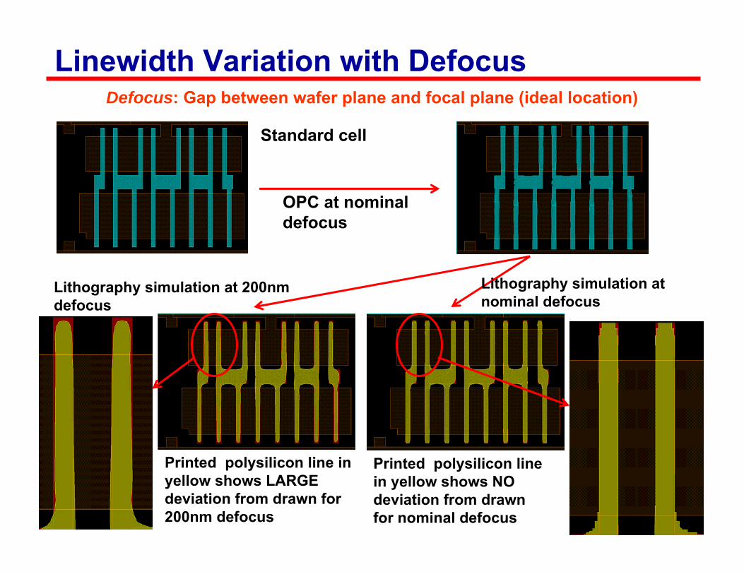
Linewidth Variation with Defocus
Standard cell
OPC at nominal defocus
Lithography simulation at nominal defocus
Lithography simulation at 200nm defocus
Printed polysilicon line in yellow shows LARGE deviation from drawn for 200nm defocus
Printed polysilicon line in yellow shows NO deviation from drawn for nominal defocus
Defocus: Gap between wafer plane and focal plane (ideal location)
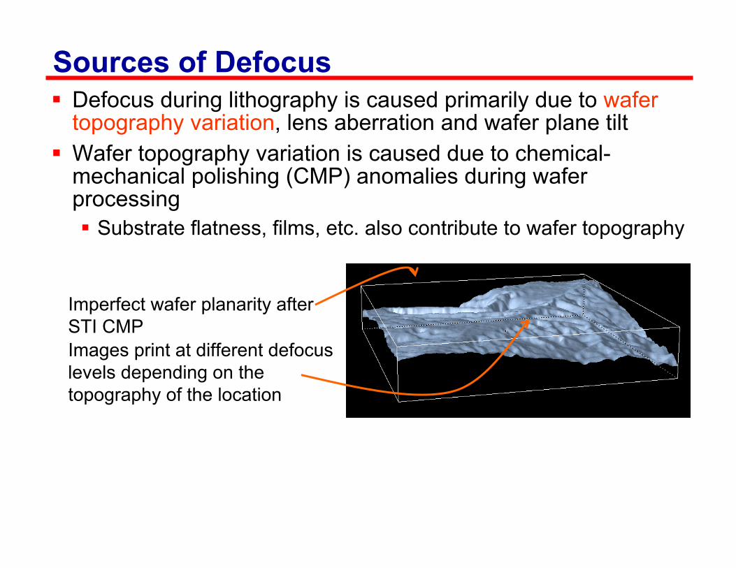
Sources of Defocus
Imperfect wafer planarity after STI CMPImages print at different defocus levels depending on the topography of the location
Defocus during lithography is caused primarily due to wafer topography variation, lens aberration and wafer plane tiltWafer topography variation is caused due to chemical-mechanical polishing (CMP) anomalies during wafer processing
Substrate flatness, films, etc. also contribute to wafer topography

Linewidth Variation with Pitch
Portion of a 90nm standard cell layout showing polysilicon lines in isolated, dense and self-compensated contexts
Dense lines linewidth > nominal
Isolated lineslinewidth < nominal
Self-compensated lines linewidth ~ nominal
Pitch of a feature: its spacing with left and right neighborsDense pitch implies small spacing, isolated or sparse pitch implies large

Across-Chip Linewidth VariationLinewidth variation compensated by OPC at nominal defocus
Bossung plot
Linewidth variation with pitch and defocus is captured in Bossung lookup tables
At defocus levels other than nominal, linewidth varies systematically with pitchFor dense pitches: linewidth increases with defocus(smiling)For isolated: linewidth decreases with defocus (frowning)At any given defocus level, linewidth for dense pitches is always greater than that of isolated pitches
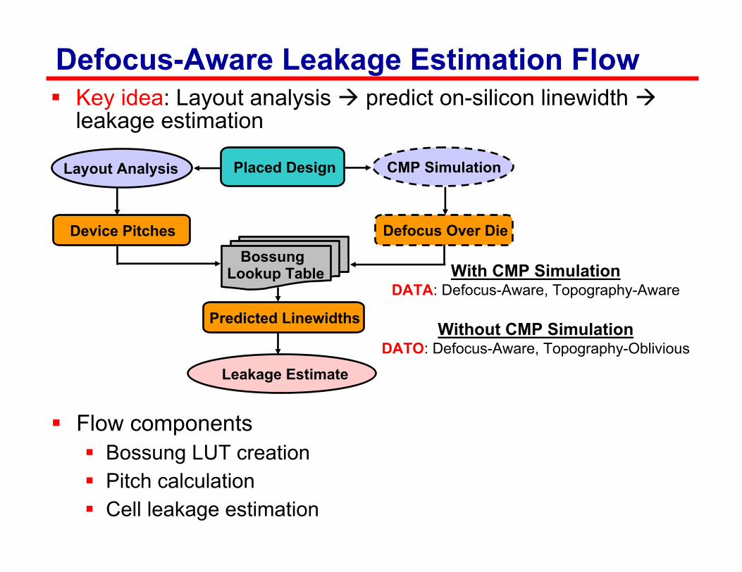
Defocus-Aware Leakage Estimation Flow
Layout Analysis Placed Design
Device Pitches
CMP Simulation
Defocus Over Die
BossungLookup Table
Predicted Linewidths
Leakage Estimate
Flow componentsBossung LUT creationPitch calculationCell leakage estimation
With CMP SimulationDATA: Defocus-Aware, Topography-Aware
Without CMP SimulationDATO: Defocus-Aware, Topography-Oblivious
Key idea: Layout analysis predict on-silicon linewidth leakage estimation
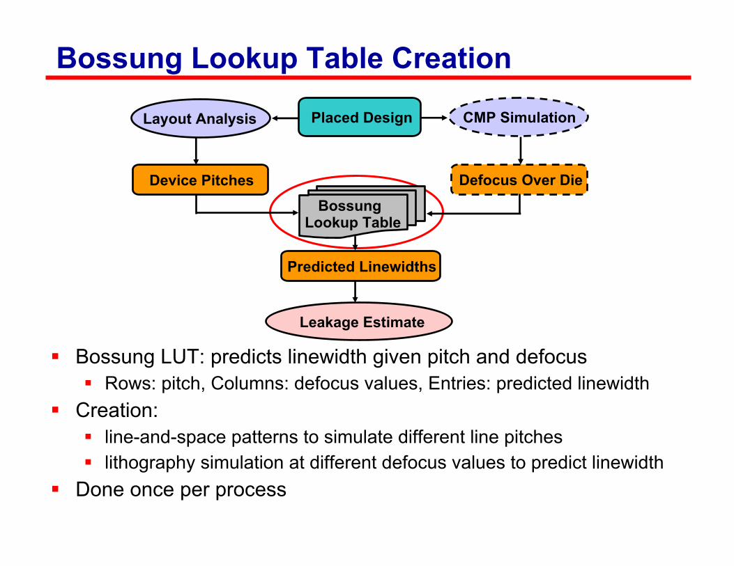
Bossung Lookup Table Creation
Layout Analysis Placed Design
Device Pitches
CMP Simulation
Defocus Over DieBossung
Lookup Table
Predicted Linewidths
Leakage Estimate
Bossung LUT: predicts linewidth given pitch and defocusRows: pitch, Columns: defocus values, Entries: predicted linewidth
Creation:line-and-space patterns to simulate different line pitcheslithography simulation at different defocus values to predict linewidth
Done once per process

Pitch Calculation
Layout Analysis Placed Design
Device Pitches
CMP Simulation
Defocus Over DieBossung
Lookup Table
Predicted Linewidths
Leakage Estimate
Layout analysis: calculates pitch given placement and cell layoutsPitch calculated from:
Cell neighbor spacing and cell orientation from placementLocation of devices within cell from LVS information

Cell Leakage EstimationLayout Analysis Placed Design
Device Pitches
CMP Simulation
Defocus Over Die
BossungLookup Table
Predicted Linewidths
Leakage Estimate
Leakage estimation: calculates cell leakage from linewidths of devices in it followed by design leakageApproach:
Cell leakage for each input state estimated by finding leaking devices by logic simulation within cell
Leakage of stacked devices neglectedDevice (NMOS and PMOS) leakage for a given gate length and widthfrom table characterized with SPICE

Experimental SetupTestcases: c5315 (2077 cells), c6288 (4776 cells), c7552 (3155 cells), alu128 (11724 cells)Cell library (20 cell) characterization with BPTM BSIM3 device models, Synopsys HSPICE, and Cadence SignalStormSynthesis with Synopsys Design Compiler with tight delay constraints. Placement with Cadence SoC Encounter.OPC, litho-simulation and scattering-bar insertion with Mentor Calibre using industry-strength recipes for 100nm linewidth and 193nm stepper.Topography used: +100nm at die center, quadratically decreases to -100nm at die corners

Leakage Estimation Results
0
1
2
3
4
5
6
7
8
9
10
c5315 c7552 c6288 alu128
Testcase
Leak
age
(mW
)
Traditional WC Traditional BC DATO WCDATO BC DATA WC DATA BC
Spread Reductionc5315: 56%c7552: 49%c6288: 49%alu128: 62%
WC: Worst CaseBC: Best Case
DATO: Defocus-Aware, Topography-ObliviousDefocus Gaussian random with µ=0nm, 3σ=200nm
DATA: Defocus-Aware, Topography-AwareDefocus Gaussian random withµ=predicted topography height3σ=100nm

Per-Instance Leakage EstimationAbility to predict leakage for each cell instance
Error distribution of traditionalleakage estimation for c6288 at nominal process corner
Can drive leakage reduction techniques like VTh assignment, input vector control, gate-length biasing(optimize cells that are more leaky)
(Negative error Traditional estimate is higher)

Gate-Length BiasingProposed by us in DAC04 and TCAD06 to reduce leakage and its variabilityKey idea: exploit VTh roll-off by increasing gate-length of non timing-critical devicesIncreasing gate-length of a cell, increases its delay, may cause other cells to become critical
Optimization problem: selection of cells to biasWe proposed a sensitivity-based greedy optimization
Bias cells in decreasing order of sensitivityRequires sensitivity updates and timing violation checks
Sensitivity of cell p = ξp = ΔLp×spΔLp : Leakage reduction of cell p upon biasingsp : Timing slack of cell p after biasing it

Defocus-Aware Gate-Length BiasingWe add defocus-awareness to gate-length biasingSensitivity-based greedy opt. in gate-length biasing
Sensitivity of cell p = ξp = ΔLp×spΔLp : Leakage reduction of cell p upon biasingsp : Timing slack of cell p after biasing it
Defocus aware sensitivity function:ξp = ‹ΔLp›×sp‹ΔLp› : Expected leakage reduction of cell p
Expected leakage reduction computation:
‹ΔLp› = ∑t ‹ΔLpt› ‹ΔLpt› : Exp. leakage reduction of device t of cell pΔLpt = f(lpt) lpt : gate-lengthlpt = g(Dpt, Ppt) Dpt : defocus; Ppt : pitch‹ΔLpt› = ∑t ∑Df(g(Dpt, Ppt)).P(Dpt) P : probability defocus is Dpt
We assume defocus (D) to be Gaussian randomTopography-oblivious: µ=0nm, 3σ=200nmTopography-aware: µ=topography height, 3σ=100nm

ResultsLeakage after traditional and defocus-aware gate-length biasing
Optimization for nominal corner and topography mentioned earlierModest leakage reductions from 2-7%10% optimization runtime increase
OutlineIntroductionSystematic Variation-Aware Techniques
Defocus-Aware Leakage Analysis and OptimizationDetailed Placement for Leakage OptimizationAberration-Aware Timing Analysis
Utilizing STI Stress in Delay Analysis and OptimizationOther Research ContributionsConclusions

Does Placement Affect Power?Conventional wisdom: Placement changes wirelength which affects dynamic power
Longer wires more C more CV2 powerLonger wires larger loading more internal power
We show placement affects leakage powerPlacement selects neighbors
neighbors of a cell determine the patterns to printpattern-dependent lithography errors affect on-silicon
gate-lengthleakage depends on gate-length
Publication: ISLPED07 (to appear)
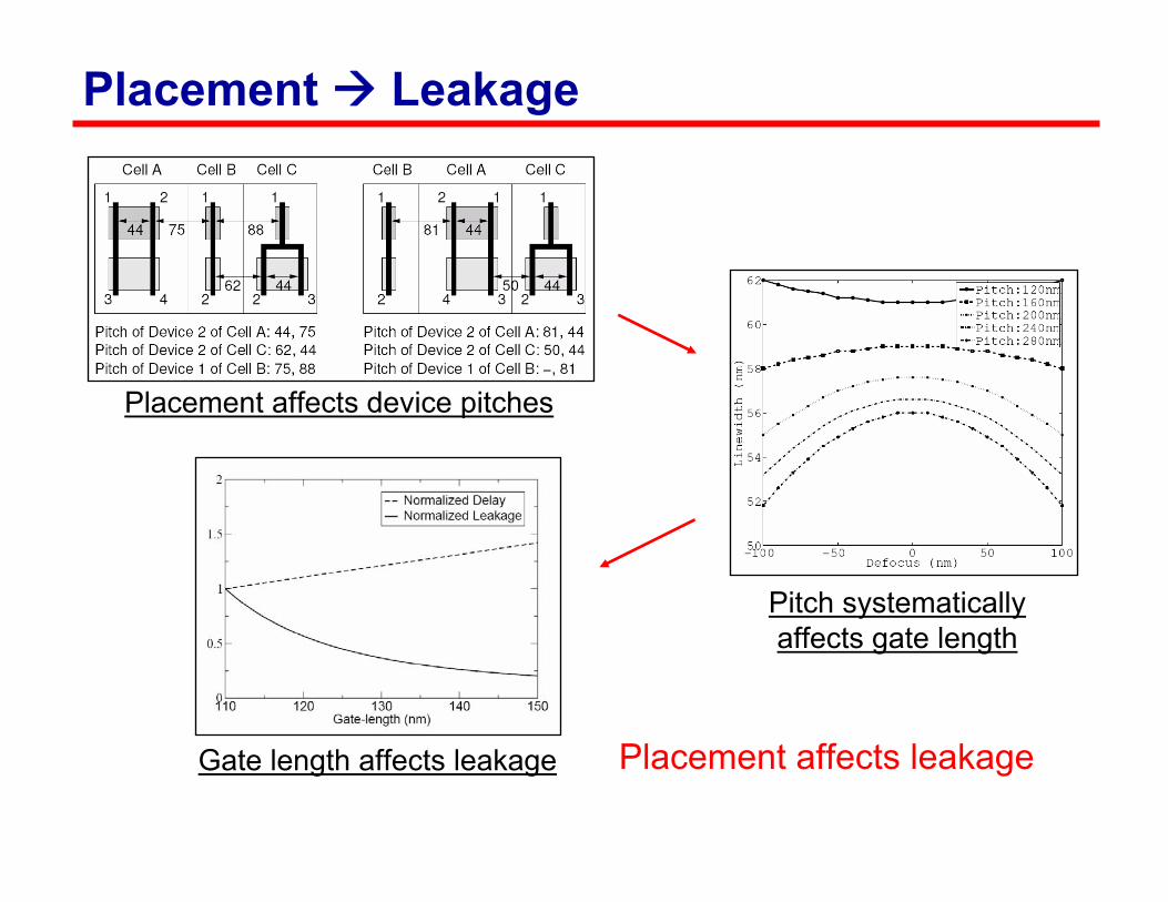
Placement Leakage
Placement affects leakage
Placement affects device pitches
Pitch systematically affects gate length
Gate length affects leakage

Detailed Placement for LeakageDetailed Placement: refinement step which performs small-range perturbations to generate a new optimized placement
Typically for wirelength and timingAffects pitches (and consequently leakage) by three knobs:
Neighbor selectionOrientationCell-to-cell spacing
Our approach:Step 1: Capture impact of placement on leakageStep 2: Utilize information in detailed placement

Capturing Placement Impact on LeakageGoal:
Construct a matrix of leakage cost
Our approach:Compute pitch when two cells abutPredict linewidth from computed pitch from Bossung plotCalculate device leakage from linewidthsCalculate cell leakage from leakage of its devices
Alternative approachesLitho-simulate abutted cells calculate device and cell leakagesOn-silicon measurements

Single-Row, No-Whitespace OptimizationOptimization done in small windows (single row)
Design partitioned into windows, cells in each window optimizedGoal: order cells and select the ones to flip to minimize leakage costWe transform the problem to the famous traveling salesman problem
Node ≡ each side of each cell (so #nodes = 2 × #cells)Complete graph with edge weight = leakage cost matrix entry
Tour gives ordering and selects cells to be flippedAll nodes (≡ each side) ordered to minimize cost (= sum of leakage cost when two edges touch)Additional constraint: two edges of the same cell must occur consecutively in tour we assign -∞ weight
We use multi-fragment greedy heuristic to solve TSP

Illustration of the Optimization
C1 C2 C3
C1 C2C3
INVX4 INVX4 NAND2X1
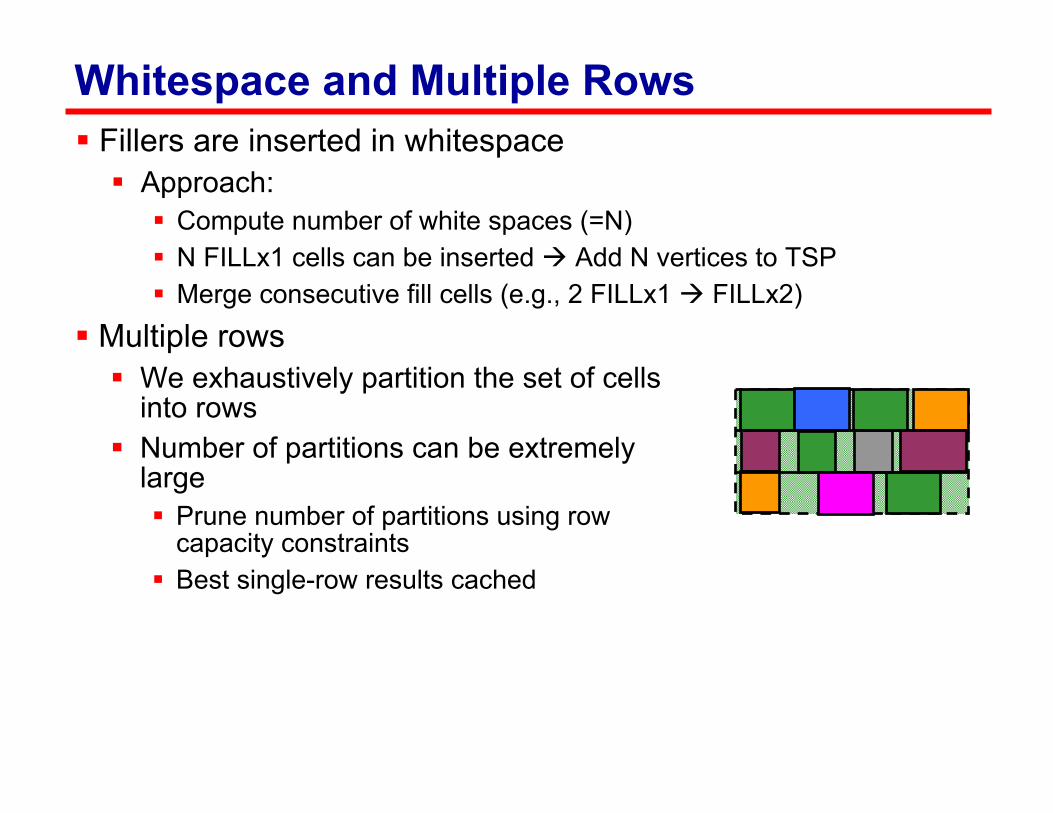
Whitespace and Multiple RowsFillers are inserted in whitespace
Approach:Compute number of white spaces (=N)N FILLx1 cells can be inserted Add N vertices to TSPMerge consecutive fill cells (e.g., 2 FILLx1 FILLx2)
Multiple rowsWe exhaustively partition the set of cells into rowsNumber of partitions can be extremely large
Prune number of partitions using row capacity constraintsBest single-row results cached

Minimizing Wirelength and Timing ImpactWirelength increase bad
Increases congestion, degrades routabilityIncreases dynamic power
Smaller window size causes smaller wirelength increaseswe increase window size progressively in phasesaccept solution of a phase if it improves upon that of last phase
Timing impact minimizedCritical cells marked as don’t-touchAll cells connected to nets of critical cells also marked as don’t-touchIncremental routing performed with nets of critical cells markedas don’t-touch

Experimental Study
Technology: 65nm dual-VTh
Tools: RTL Compiler, SoC Encounter, OpenAccessTestcases: AES (80% util), AES (85% util), DES (73% util)

Results
Results for testcase AES (80% utilization)
† identifies results with our measures to minimize wirelength and timing bypassedAs expected, larger windows
improve leakage, but;increase wirelength and dynamic power.

OutlineIntroductionSystematic Variation-Aware Techniques
Defocus-Aware Leakage Analysis and OptimizationDetailed Placement for Leakage OptimizationAberration-Aware Timing Analysis
Utilizing STI Stress in Delay Analysis and OptimizationOther Research ContributionsConclusions
Lens AberrationLens aberrations: image distortions due to imperfect lens
Variety of effects on lithographic imaging shifts in image position, image asymmetry, reduction of process window
Zernike aberration coefficientsrepresent wavefront aberrations (36 terms)Coma image asymmetry, pattern-dependent image shiftAstigmatism CD difference between horizontal, vertical linesSpherical changes best DOF between dense/isolated patterns
Lens field: wafer area exposed in one shotAberration (and Zernike’s coefficients) vary with position in the lens field gate length varies with position in lens field

Impact on Gate Length (CD)
Impact on average CD varies with location in lens field
Average CD 93nm – 97nm for NAND2X4
85
90
95
100
-11.25 -8.75 -6.25 -3.75 -1.25 0 1.25 3.75 6.25 8.75 11.25
Lens Position (mm)
Ave
rage
CD
(nm
)NAND2X4 NOR2X1INVX2 NAND3X4Different devices in a cell
affected differently CD skew induced
different
Reticle (mask) mapsame
Slit scans from one side of the field to another
Zernike coefficients vary with position in the lens field
CD varies along horizontal direction CD constant along vertical direction
Gate delay depends on CD Gate delay depends on position in lens field

Impact on Gate Delay
Impact on average cell delay varies with location in lens field
NAND2X4 delay varies between -2% and 2%
Input capacitance and slews increase with CD
Predictable “fast” and “slow” regions due to aberrationAccount for delay variations induced by aberration in timing analysisAlso: place setup-critical cells in the fast regions, and place hold-critical cells in the slow regions (DATE06)

Standard Timing Analysis Flow
Standard Cell GDS
SPICE Netlist
LibraryCharacterization
SPICE Model
Delay Calculation
Problem: With aberration, two instances of the same master should have different timing models !

Aberration-Aware Timing FlowStandard Cell GDS
Print ImageGDS
19 Lens Positions
SRAF Generation
OPC
Lithography Simulation
CD Measurement
SPICE Netlist
LibraryCharacterization
Transistor-levelTiming Library
Delay LUTs
LVS
SPICE Model
Cell variant created in library for each lens positionTwo main steps:
Construct litho models get simulated gate CDs of each instanceGenerate timing library models of all masters for different locations
Timing library used along with placement in STA
CD Measurement
Zernike’sCoefficients
19
1
(for use in placer)
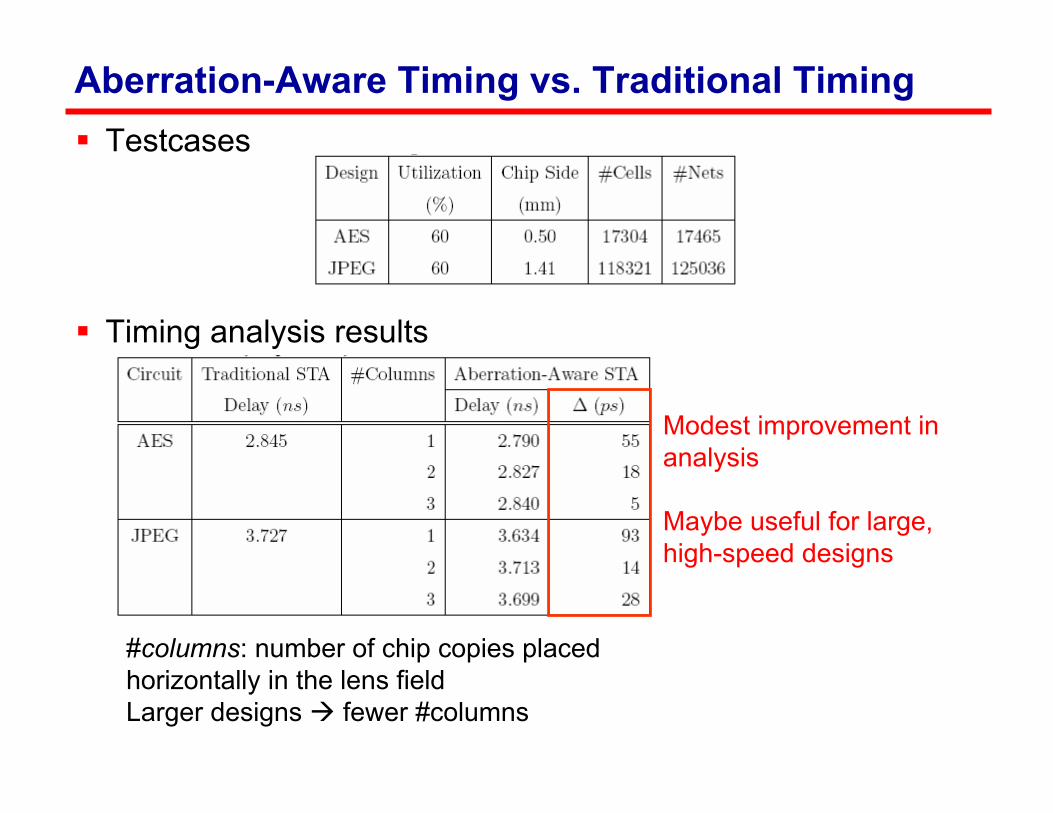
Aberration-Aware Timing vs. Traditional TimingTestcases
Timing analysis results
#columns: number of chip copies placed horizontally in the lens fieldLarger designs fewer #columns
Modest improvement in analysis
Maybe useful for large, high-speed designs
OutlineIntroductionSystematic Variation-Aware Techniques
Defocus-Aware Leakage Analysis and OptimizationDetailed Placement for Leakage OptimizationAberration-Aware Timing Analysis
Utilizing STI Stress in Delay Analysis and OptimizationOther Research ContributionsConclusions

What Is STI Stress?STI surrounds devices to electrically isolate themSide profile
STI pushes active region inwardsSmaller active region gets pushed more
more stressLarger STI region pushes more
more stressStress enhances PMOS mobility and performance, degrades NMOS mobility and performance
Active STIPolysilicon
Active STI
Polysilicon
S DG

Present BSIM Stress ModelingStress partially modeled since BSIM 4.3.0
Parameters SA, SB, SC addedParameters capture gate to STI separation
Stress effect due to STI width (STIW) not modeledSTI width determined by placement
Cannot be calculated at cell netlist level in characterizationNew flow needed to annotate STIW information from placement
Smaller in extent than due to gate-active edge separationWe multiply BSIM mobility by our correction factor mobWe construct a mob model using Sentaurus process simulationsWe plug in our mob model as a function of STI width parameters set from placement

STI Stress Compact ModelingProcess simulation until gate deposition using Synopsys SentaurusSimulations performed for different STI widths on left and right, SA, SB
Simulated stress converted to mobility using [Smith65] and normalizedMobility models derived using curve-fitting to simulated data
Several other STI heights and stress liners simulated STI width changes by <10% STI width effects significant for most processes
NMOS PMOS

STI Stress-Aware Timing AnalysisAdded STIW parameters:
PL, PR, NL, NRPL: Distance between cell boundary and positive active region edge of left neighbor
PlacedDesign
Static TimingAnalysis
SPICE forCritical Paths
AnnotateSTIW Params
AnnotatedSPICE
SPICESimulation
STI Stress-Aware Timing Analysis Flow
We use this flow to evaluate our optimization

Optimization: Exploiting Stress for Performance
Goal: engineer STIW such that stress speeds PMOS and NMOSHigh stress improves PMOS increase STIW for PMOSLow stress improves NMOS decrease STIW for NMOSKnobs to alter STIW
Active layer fill insertionPlacement perturbation
Active layer fill insertion
Fill inserted next to N-diffusion (NRX) Small STIW for NMOSNo fill next to P-diffusion (PRX) Large STIW for PMOS
After Active Layer FillGeneric Cell Layout

Placement PerturbationIncrease spacing for timing critical cells
Increases PMOS STIW better PMOS speedCreate spacing for active fill for NMOS that was previously not possible
better NMOS speedMinimize adverse timing impact of placement perturbation
Don’t modify locations of critical cells, their routes, clock tree, etc.
Don’t Touch Cell Timing Critical Cells
Before Optimization
After PlacementPerturbation
After Placement and Fill Optimization

Stress-Aware vs. Traditional Timing AnalysisCircuit-level stress-aware vs. traditional timing analysis
Traditional timing analysis worst-cases stress effects for correctnessStress-aware analysis models stress correct and less pessimistic
0.00%
1.00%
2.00%
3.00%
4.00%
5.00%
6.00%
7.00%
c5315 ALU s38417 AES
MCTTPD
MCT: Minimum cycle time
TPD: Top paths delay (= sum of delays of top 100 critical paths)
5.75% smaller MCT on average

Results: Delay Optimization
Smaller delay reduction for s38417 because >50% cells are flops and marked don’t-touch.Negligible wirelength increase (<0.67%)
Path delay histogram for test case AES
0.00%
1.00%
2.00%
3.00%
4.00%
5.00%
6.00%
7.00%
8.00%
c5315 ALU s38417 AES
MCTTPD
4.37% average reduction in MCT5.15% average reduction in TPD

OutlineIntroductionSystematic Variation-Aware Techniques
Defocus-Aware Leakage Analysis and OptimizationDetailed Placement for Leakage OptimizationAberration-Aware Timing Analysis
Utilizing STI Stress in Delay Analysis and OptimizationOther Research ContributionsConclusions

Other Contributions Under This ThemeGate-length biasing
Motivation: leakage and its variability are critical concernsKey idea: exploit VTh roll-off by increasing gate-length of non timing-critical devicesReduces leakage and its variability significantly
STI fill for CMPMotivation: Imperfect CMP causes device failure, device latch-up, and leakage. Expensive reverse etchback used to rectifyHigh nitride density and low oxide-density variation addresses above shortcomingsOxide deposited over nitride with a slanting sidewall nitride features determine nitride and oxide densityKey idea: size and shape nitride features to control nitride and oxide densityProposed fill insertion to maximize nitride density and minimize oxide density variationResults from CMP simulation showed superior post-CMP topography and planarization window
Impact of floating fill on interconnect capacitanceMotivation: floating fill affects capacitance of wires and no reliable full-chip extraction methods existStudied impact of floating fill on neighboring interconnects on the same layerPerformed field solver simulations to understand the capacitive impact of different fill sizes and configurations Proposed fill insertion guidelines to reduce capacitive effect

ConclusionsDFM: measures taken in design to enhance yieldFocus of my work: manufacturing-aware physical design techniques to increase yield by:
Reducing process variationsImproving design robustnessAccounting for systematic variations in analyses and optimizations
Looking forwardManufacturing technology will improve, but process variability as a percentage will not reduce novel DFM methods will be neededSeveral challenges exist to adoption of novel DFM methods (e.g.,acquisition of variational data)Traditional DFM will continue to be crucialTechniques to reduce variability and enhance robustness will be deployed first, followed by statistical and systematic variation-aware methods.

Thank You!Questions?

Backup
Gate-Length Biasing for Leakage Control

Leakage and Leakage Variability
Proposed gate-length biasing to control leakage and its variability. Publications:
Gate-biasing in TCAD06 and DAC04Its impact on Vth selection in ISQED06
Contribution of leakage to total power increasing
Near-exponential dependence of leakage on gate-length
Even small gate-length variability Large leakage variability

Gate-Length BiasingKey Idea 1: Slightly increase (bias) the LGate of devices
00.20.40.60.8
11.2
130
132
134
136
138
140
Gate-length (nm)
LeakageDelay
Variation of leakage and delay (each normalized to 1) for an NMOS device in an industrial 130nm technology
Impact onLeakage and Delay
Reduce leakage?
Reduce leakage variability?
Key Idea 2: Bias only non- timing-critical devices No loss in circuit performance
Impact onLeakage Variability
Gate-length
Leak
age
Gate-length
Leak
age
Drawn LGate
Bia
sing
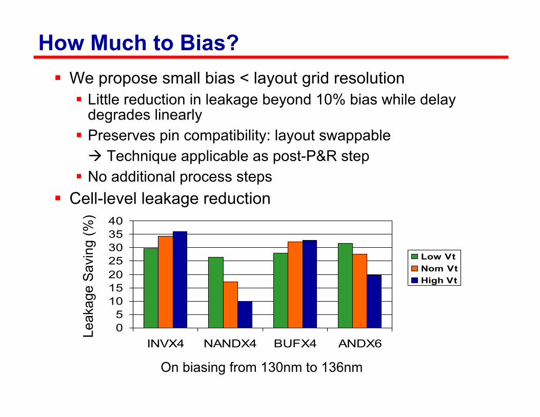
How Much to Bias?We propose small bias < layout grid resolution
Little reduction in leakage beyond 10% bias while delay degrades linearlyPreserves pin compatibility: layout swappable
Technique applicable as post-P&R stepNo additional process steps
Cell-level leakage reduction
05
10152025303540
INVX4 NANDX4 BUFX4 ANDX6
Low VtNom VtHigh Vt
Leak
age
Sav
ing
(%)
On biasing from 130nm to 136nm

Methodology
Extend a cell library with biased LGate versions of all cellsOptimize circuit for leakage by using biased LGate versions for non-critical cells
Characterize
HSPICE
Spicemodels
Low VT, Nominal LGateLow VT, Biased LGate
Nominal VT, Nominal LGateNominal VT, Biased LGate
Generated Library
Circuit Optimizer
Gate-LevelCircuit Netlist
OptimizedCircuit Netlist
Leakage OptimizerOff-the-shelf sizing tools (e.g., SNPS DC) do not work well
Tradeoffs involved different from traditional cell (width) sizingFirst approach: sensitivity-based downsizing
Start with a netlist with no timing violationsDownsize (i.e., delay increases, leakage decreases) iteratively
Order by sensitivityCheck timing after each or a couple of downsizing moves
EnhancementsTransistor-level optimizationBulk moves (=simultaneous downsizing of a group of cells)
Cells in different pipeline stagesCells at same topological level
Lagrangian relaxationConstraints and objectives expressed as convex functionsIteratively improving solution (modeling inaccuracy improves each iteration)Better quality but more runtime

0
0.2
0.4
0.6
0.8
1
1.2
s923
4c5
315
c755
2s1
3207
c628
8alu
128
s384
17
Nor
mal
ized
Lea
kage
SVT-SGLSVT-DGLDVT-SGLDVT-DGL
29%13% 21%
29%
7% 13%
29%
27%10%
2%
28%
1%
20% 17%
Results: Leakage Reduction
Single VThSingleGateLength
Dual VTh
DualGateLength
Dual-VTh is the mainstream leakage reduction techniqueAssess leakage reduction with and without dual-VThtechnique

Results: Leakage Variability
Leakage variability estimated with 10,000 Monte-Carlo simulations on alu128σWID = σDTD = 3.3nm(Variations in gate-length assumed to be Gaussian w/ zero correlation)
0.00%
10.00%
20.00%
30.00%
40.00%
50.00%
60.00%
c5315 c6288 c7552 alu128
Percentage Reduction in Leakage Spread

Backup
STI Fill for CMP

CMP for STISTI mainstream CMOS isolation technologyIn STI, substrate trenches filled with oxide surround devices or group of devices that need to be isolatedRelevant process steps:
Diffusion (OD) regions covered with nitrideTrenches created where nitride absent and filled with oxideChemical Mechanical Polishing (CMP) to planarize and remove excess oxide over nitride (overburden oxide)
SiSi
Oxide Nitride
Before CMPBefore CMP After Perfect CMPAfter Perfect CMPCMP goal: Perfectly planar nitride and trench oxide surface

CMP is Not Perfect
Planarization window: Time window to stop CMPStopping sooner leaves oxide over nitrideStopping later polishes silicon under nitrideLarger planarization window desirable
Step height: Oxide thickness variation after CMPQuantifies oxide dishingSmaller step height desirable
CMP quality depends on nitride and oxide densityControl nitride and oxide density to enlarge planarization window and to decrease step height
Failure to clear oxide Nitride erosion Oxide dishing
Key Failures Caused by Imperfect CMP

CMP is pattern dependent Fill insertion improves planarization window and step height
Deposition bias: Oxide over nitride deposited with slanted profile Oxide features are “shrunk” nitride features
Size and shape fill to control nitride and oxide density
Fill Insertion
Top view of layout
Diffusion/Nitride
Area available for fill insertion
α α
Oxide
Nitride
Shrinkage = α
Top View

Objectives for Fill InsertionPrimary goals:
Enlarge planarization window Minimize step height i.e., post-CMP oxide height variation
Minimize oxide density variationOxide uniformly removed from all regionsEnlarges planarization window as oxide clears simultaneously
Maximize nitride densityEnlarges planarization window as nitride polishes slowly
Objective 1: Minimize oxide density variationObjective 2: Maximize nitride density

Dual-Objective Problem Formulation
Dummy fill formulationGiven:
STI regions where fill can be insertedShrinkage α
Constraint:No DRC violations (such as min. spacing, min .width, min. area, etc.)
Objectives:1. minimize oxide density variation2. maximize nitride density

Density Variation Minimization with LPMinimize oxide density variation
Use previously proposed LP-based solutionLayout area divided into n x n tilesDensity computed over sliding windows (= w x w tiles)Inputs:
min. oxide density (|OxideMin|) per tileTo compute: shrink design’s nitride features by α
max. oxide density (|OxideMax|) per tileTo compute: insert max. fill, shrink nitride features by α
Output: target oxide density (|OxideTarget|) per tileDual-objective single-objective (nitride density) problem with oxide density constrained to |OxideTarget |
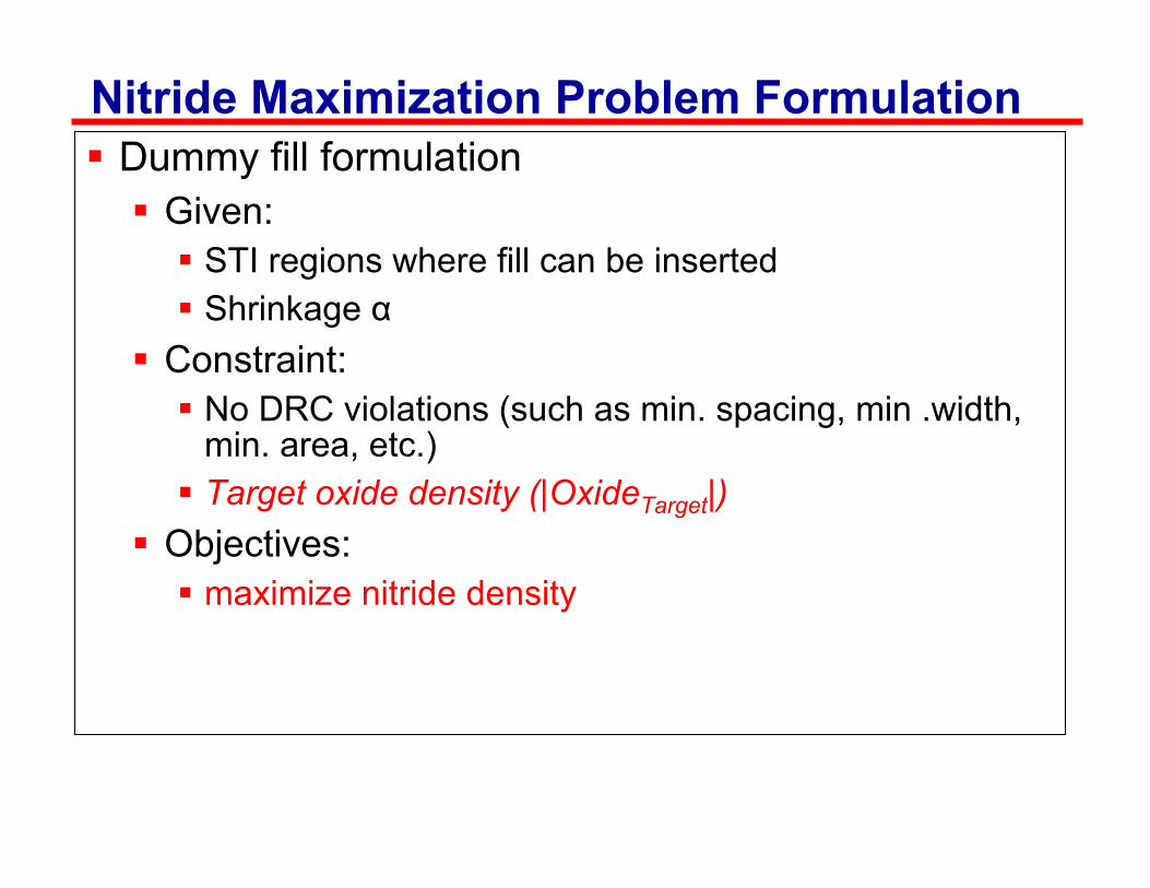
Nitride Maximization Problem FormulationDummy fill formulation
Given:STI regions where fill can be insertedShrinkage α
Constraint:No DRC violations (such as min. spacing, min .width, min. area, etc.)Target oxide density (|OxideTarget|)
Objectives:maximize nitride density

Case Analysis Based Solution Given |OxideTarget |, insert fill for max. nitride densitySolution (for each tile) based on case analysis
Case 1: |OxideTarget | = |OxideMax| Case 2: |OxideTarget | = |OxideMin|Case 3: |OxideMin| < |OxideTarget | < |OxideMax|
Case 1 Insert max. nitride fillFill nitride everywhere where it can be addedMin. OD-OD (diffusion-diffusion) spacing ≈ 0.15µMin. OD width ≈ 0.15µOther OD DRCs: min. area, max. width, max. areaLayout OD-OD Spacing Min. OD Width
Feature Nitride STI Well Diffusion expanded by min. spacing
Max. nitride fillWidth too small
} More common due to nature of LP

Case 2: |OxideTarget | = |OxideMin|Need to insert fill that does not increase oxide densityNaïve approach: insert fill rectangles of shorter side < αBetter approach: perform max. nitride fill then dig square holes of min. allowable side β
Gives higher nitride:oxide density ratio
No oxide density in rounded square around a holeCover nitride with rounded squares no oxide density
β
ααNitride Hole
No oxide in this region
Top View
Covering with rounded squares difficult approximate rounded squares with inscribed hexagonsCover rectilinear max. nitride with min. number of hexagons proposed a new algorithm
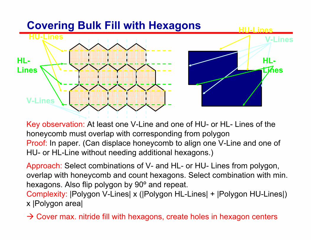
Covering Bulk Fill with HexagonsHU-Lines
V-Lines
HL-Lines
V-LinesHU-Lines
HL-Lines
Key observation: At least one V-Line and one of HU- or HL- Lines of the honeycomb must overlap with corresponding from polygonProof: In paper. (Can displace honeycomb to align one V-Line and one of HU- or HL-Line without needing additional hexagons.)
Approach: Select combinations of V- and HL- or HU- Lines from polygon, overlap with honeycomb and count hexagons. Select combination with min. hexagons. Also flip polygon by 90º and repeat.Complexity: |Polygon V-Lines| x (|Polygon HL-Lines| + |Polygon HU-Lines|) x |Polygon area|
Cover max. nitride fill with hexagons, create holes in hexagon centers

Case 3: |OxideMin| < |OxideTarget | < |OxideMax|Holes give high nitride:oxide density
insert max. nitride fill and create holes to reduce oxide densityOK for nitride fill to contribute to oxide density
approximate rounded squares by circumscribed hexagons
When max. nitride is covered with circumscribed hexagons, oxide density increases
If oxide density (=outloss x max. nitride area) < |OxideTarget| increase oxide density by filling some holesIf oxide density > |OxideTarget| decrease oxide density by partially using Case 2 solution
Outloss = Oxide Area
Nitride Area

Solution SummaryDivide layout into tilesCalculate |OxideMin| and |OxideMax|Run LP-based fill synthesis for oxide variation minimization Get |OxideTarget |If |OxideTarget | = |OxideMax| (i.e., max. oxide needed)
Add max. nitride fillIf |OxideTarget | = |OxideMin| (i.e., add no more oxide)
Add max. nitride fillCalculate inscribed hexagon size based on α and βCover max. nitride fill with hexagonsCreate square holes in the center of hexagons
If |OxideMin| < |OxideTarget | < |OxideMax| (i.e., general case)Add max. nitride fillCalculate circumscribed hexagon size based on α and βCover max. nitride fill with hexagonsCreate square holes in the centers of hexagonsIf oxide density lower than needed fill some holesIf oxide density higher than needed Use inscribed hexagons in some
region

Experimental SetupTwo types of studies
Density analysisPost-CMP topography assessment using CMP simulator
Comparisons between:UnfilledTile-based fill (DRC-correct fill squares inserted)Proposed fill
Our testcases: 2 large designs created by assembling smaller ones
“Mixed”: RISC + JPEG + AES + DES2mm x 2mm, 756K cells“OpenRisc8”: 8-core RISC + SRAM2.8mm x 3mm, 423K cells + SRAM

Layout After Fill Insertion
Tiling-based fill Fill with proposed approach
Inserted fill
Designfeatures
+ Higher nitride density+ Smaller variation in STI well size less variation in STI stress

Density Enhancement Results
Testcase: Mixed Testcase: OpenRisc8
Unfilled Tiled 0.5µ/0.5µ Tiled 1.0µ/0.5µ Tiled 1.0µ/1.0µ
Proposed
+ Significantly higher nitride density+ Lower oxide density variation
0%10%20%30%40%50%60%70%
Max. OxideDensity Var.
Min. NitrideDensity
Av. NitrideDensity
0%10%20%30%40%50%60%70%
Max. Oxide DensityVar.
Min. Nitride Density Av. Nitride Density
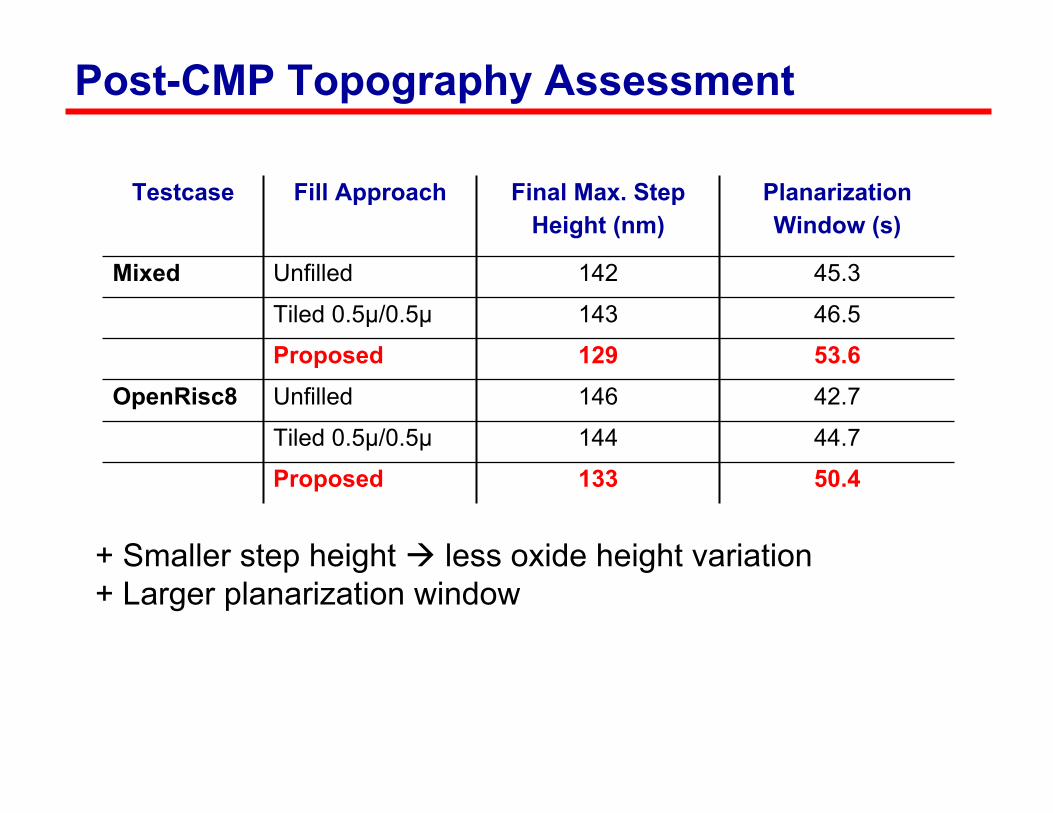
Post-CMP Topography Assessment
133144
146
129143
142
Final Max. Step Height (nm)
50.4Proposed44.7Tiled 0.5µ/0.5µ
42.7UnfilledOpenRisc853.6Proposed46.5Tiled 0.5µ/0.5µ
45.3 UnfilledMixed
Planarization Window (s)
Fill ApproachTestcase
+ Smaller step height less oxide height variation+ Larger planarization window