Embed Size (px)
Citation preview

IS62WV10248EALL/BLL IS65WV10248EALL/BLL
Integrated Silicon Solution, Inc.- www.issi.com 1 Rev. C1
03/06/2017
1Mx8 LOW VOLTAGE, ULTRA LOW POWER CMOS STATIC RAM
KEY FEATURES
High-speed access time: 45ns, 55ns
CMOS low power operation – 36 mW (typical) operating
TTL compatible interface levels
Single power supply
–1.65V-2.2V VDD (62/65WV10248EALL)
– 2.2V-3.6V VDD (62/65WV10248EBLL)
Automotive temperature (-40oC to +125
oC)
Lead-free available
DESCRIPTION The ISSI IS62WV10248EALL/ IS62WV10248EBLL are high-speed, 8M bit static RAMs organized as 1M words by 8 bits. It is fabricated using ISSI's high-performance CMOS technology. This highly reliable process coupled with innovative circuit design techniques, yields high-performance and low power consumption devices.
When is HIGH (deselected) or when CS2 is low (deselected), the device assumes a standby mode at which the power dissipation can be reduced down with CMOS input levels. Easy memory expansion is provided by using Chip Enable and Output Enable inputs. The active LOW
Write Enable ( ) controls both writing and reading of the memory. The IS62WV10248EALL and IS62WV10248EBLL are packaged in the JEDEC standard 48-pin mini BGA (6mm x 8mm) and 44-Pin TSOP (TYPE II).
BLOCK DIAGRAM
Copyright © 2017 Integrated Silicon Solution, Inc. All rights reserved. ISSI reserves the right to make changes to this specification and its products at any time without notice. ISSI assumes no liability arising out of the application or use of any information, products or services described herein. Customers are advised to obtain the latest version of this device specification before relying on any published information and before placing orders for products. Integrated Silicon Solution, Inc. does not recommend the use of any of its products in life support applications where the failure or malfunction of the product can reasonably be expected to cause failure of the life support system or to significantly affect its safety or effectiveness. Products are not authorized for use in such applications unless Integrated Silicon Solution, Inc. receives written assurance to its satisfaction, that: a.) the risk of injury or damage has been minimized; b.) the user assume all such risks; and
c.) potential liability of Integrated Silicon Solution, Inc is adequately protected under the circumstances
MARCH 2017
IS62WV10248EALL/BLL IS65WV10248EALL/BLL
Integrated Silicon Solution, Inc.- www.issi.com 2 Rev. C1
03/06/2017
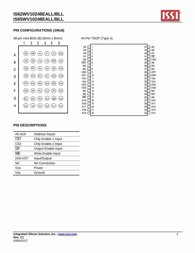
PIN CONFIGURATIONS (1Mx8) 48-pin mini BGA (B) (6mm x 8mm)
44-Pin TSOP (Type II)
PIN DESCRIPTIONS
A0-A19 Address Inputs
Chip Enable 1 Input
CS2 Chip Enable 2 Input
Output Enable Input
Write Enable Input
I/O0-I/O7 Input/Output
NC No Connection
VDD Power
Vss Ground
IS62WV10248EALL/BLL IS65WV10248EALL/BLL
Integrated Silicon Solution, Inc.- www.issi.com 3 Rev. C1
03/06/2017
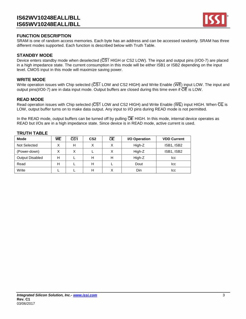
FUNCTION DESCRIPTION SRAM is one of random access memories. Each byte has an address and can be accessed randomly. SRAM has three different modes supported. Each function is described below with Truth Table.
STANDBY MODE Device enters standby mode when deselected ( HIGH or CS2 LOW). The input and output pins (I/O0-7) are placed in a high impedance state. The current consumption in this mode will be either ISB1 or ISB2 depending on the input level. CMOS input in this mode will maximize saving power.
WRITE MODE Write operation issues with Chip selected ( LOW and CS2 HIGH) and Write Enable ( ) input LOW. The input and
output pins(I/O0-7) are in data input mode. Output buffers are closed during this time even if is LOW.
READ MODE Read operation issues with Chip selected ( LOW and CS2 HIGH) and Write Enable ( ) input HIGH. When is LOW, output buffer turns on to make data output. Any input to I/O pins during READ mode is not permitted.
In the READ mode, output buffers can be turned off by pulling HIGH. In this mode, internal device operates as READ but I/Os are in a high impedance state. Since device is in READ mode, active current is used.
TRUTH TABLE
Mode CS2 I/O Operation VDD Current
Not Selected X H X X High-Z ISB1, ISB2
(Power-down) X X L X High-Z ISB1, ISB2
Output Disabled H L H H High-Z Icc
Read H L H L Dout Icc
Write L L H X Din Icc
IS62WV10248EALL/BLL IS65WV10248EALL/BLL
Integrated Silicon Solution, Inc.- www.issi.com 4 Rev. C1
03/06/2017
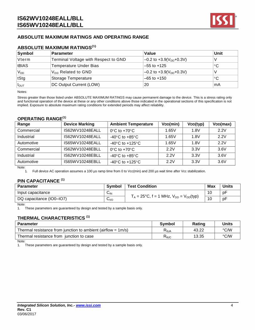
ABSOLUTE MAXIMUM RATINGS AND OPERATING RANGE ABSOLUTE MAXIMUM RATINGS(1)
Symbol Parameter Value Unit
Vterm Terminal Voltage with Respect to GND –0.2 to +3.9(VDD+0.3V) V
tBIAS Temperature Under Bias –55 to +125 C
VDD VDD Related to GND –0.2 to +3.9(VDD+0.3V) V
tStg Storage Temperature –65 to +150 C
IOUT DC Output Current (LOW) 20 mA Notes:
Stress greater than those listed under ABSOLUTE MAXIMUM RATINGS may cause permanent damage to the device. This is a stress rating only and functional operation of the device at these or any other conditions above those indicated in the operational sections of this specification is not implied. Exposure to absolute maximum rating conditions for extended periods may affect reliability.
OPERATING RANGE(1)
Range Device Marking Ambient Temperature VDD(min) VDD(typ) VDD(max)
Commercial IS62WV10248EALL 0C to +70C 1.65V 1.8V 2.2V
Industrial IS62WV10248EALL -40C to +85C 1.65V 1.8V 2.2V
Automotive IS65WV10248EALL -40C to +125C 1.65V 1.8V 2.2V
Commercial IS62WV10248EBLL 0C to +70C 2.2V 3.3V 3.6V
Industrial IS62WV10248EBLL -40C to +85C 2.2V 3.3V 3.6V
Automotive IS65WV10248EBLL -40C to +125C 2.2V 3.3V 3.6V
Note: 1. Full device AC operation assumes a 100 µs ramp time from 0 to Vcc(min) and 200 µs wait time after Vcc stabilization.
PIN CAPACITANCE (1) Parameter Symbol Test Condition Max Units
Input capacitance CIN TA = 25°C, f = 1 MHz, VDD = VDD(typ)
10 pF
DQ capacitance (IO0–IO7) CI/O 10 pF
Note: 1. These parameters are guaranteed by design and tested by a sample basis only.
THERMAL CHARACTERISTICS (1)
Parameter Symbol Rating Units
Thermal resistance from junction to ambient (airflow = 1m/s) RθJA 43.22 °C/W
Thermal resistance from junction to case RθJC 13.35 °C/W Note: 1. These parameters are guaranteed by design and tested by a sample basis only.

IS62WV10248EALL/BLL IS65WV10248EALL/BLL
Integrated Silicon Solution, Inc.- www.issi.com 5 Rev. C1
03/06/2017
ELECTRICAL CHARACTERISTICS IS62(5)WV10248EALL DC ELECTRICAL CHARACTERISTICS-I (OVER THE OPERATING RANGE)
Symbol Parameter Test Conditions Min. Max. Unit
VOH Output HIGH Voltage IOH = -0.1 mA 1.4 — V
VOL Output LOW Voltage IOL = 0.1 mA — 0.2 V
VIH(1)
Input HIGH Voltage 1.4 VDD + 0.2 V
VIL(1)
Input LOW Voltage –0.2 0.4 V
ILI Input Leakage GND < VIN < VDD –1 1 µA
ILO Output Leakage GND < VIN < VDD, Output Disabled –1 1 µA Notes: 1. VILL(min) = -1.0V AC (pulse width < 10ns). Not 100% tested.
VIHH (max) = VDD + 1.0V AC (pulse width < 10ns). Not 100% tested.
IS62(5)WV10248EBLL DC ELECTRICAL CHARACTERISTICS-I (OVER THE OPERATING RANGE)
Symbol Parameter Test Conditions Min. Max. Unit
VOH Output HIGH Voltage 2.2 ≤ VDD < 2.7, IOH = -0.1 mA 2.0 — V
2.7 ≤ VDD ≤ 3.6, IOH = -1.0 mA 2.4 — V
VOL Output LOW Voltage 2.2 ≤ VDD < 2.7, IOL = 0.1 mA — 0.4 V
2.7 ≤ VDD ≤ 3.6, IOL = 2.1 mA — 0.4 V
VIH(1)
Input HIGH Voltage 2.2 ≤ VDD < 2.7 1.8 VDD + 0.3 V
2.7 ≤ VDD ≤ 3.6 2.2 VDD + 0.3 V
VIL(1)
Input LOW Voltage 2.2 ≤ VDD < 2.7 –0.3 0.6 V
2.7 ≤ VDD ≤ 3.6 –0.3 0.8 V
ILI Input Leakage GND < VIN < VDD –1 1 µA
ILO Output Leakage GND < VIN < VDD, Output Disabled –1 1 µA Notes: 1. VILL(min) = -2.0V AC (pulse width < 10ns). Not 100% tested.
VIHH (max) = VDD + 2.0V AC (pulse width < 10ns). Not 100% tested.

IS62WV10248EALL/BLL IS65WV10248EALL/BLL
Integrated Silicon Solution, Inc.- www.issi.com 6 Rev. C1
03/06/2017
IS62(5)WV10248EALL DC ELECTRICAL CHARACTERISTICS-II FOR POWER (OVER THE OPERATING RANGE)
Symbol Parameter Test Conditions Grade Typ. Max. Unit
ICC VDD Dynamic Operating Supply Current
VDD=VDD(max), IOUT=0mA, f=fMAX Com. - 12 mA
Ind. - 15
Auto. - 15
ICC1 VDD Static Operating Supply Current
VDD=VDD(max), IOUT = 0mA, f=0Hz Com. - 6 mA
Ind. - 6
Auto. - 6
ISB2 CMOS Standby Current (CMOS Inputs)
VDD=VDD(max), (1) 0V ≤ CS2 ≤ 0.2V or
(2) ≥ VDD - 0.2V, CS2 ≥ VDD - 0.2V
Com.
25oC 11.1 15
µA
45oC 11.4 17
70oC 13.6 20
Ind./Auto A1 15.1 25
Auto. A3 28.4 50
Note: 1. Typical values are measured at VDD = 1.8V and not 100% tested.
IS62(5)WV10248EBLL DC ELECTRICAL CHARACTERISTICS-II FOR POWER (OVER THE OPERATING RANGE)
Symbol Parameter Test Conditions Grade Typ. Max. Unit
ICC VDD Dynamic Operating Supply Current
VDD=VDD(max), IOUT=0mA, f=fMAX Com. - 15 mA
Ind. - 15
Auto. - 15
ICC1 VDD Static Operating Supply Current
VDD=VDD(max), IOUT = 0mA, f=0Hz Com. - 6 mA
Ind. - 6
Auto. - 6
ISB2 CMOS Standby Current (CMOS Inputs)
VDD=VDD(max), (1) 0V ≤ CS2 ≤ 0.2V or
(2) ≥ VDD - 0.2V, CS2 ≥ VDD - 0.2V
Com.
25oC 11.1 15
µA
45oC 11.4 17
70oC 13.6 20
Ind./Auto A1 15.1 25
Auto. A3 28.4 50
Note: 1. Typical values are measured at VDD = 3.0V, and not 100% tested.
IS62WV10248EALL/BLL IS65WV10248EALL/BLL
Integrated Silicon Solution, Inc.- www.issi.com 7 Rev. C1
03/06/2017
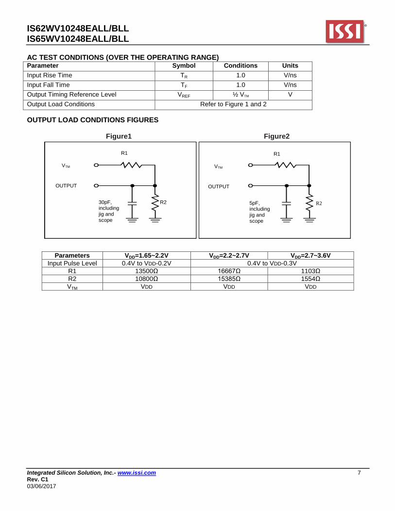
AC TEST CONDITIONS (OVER THE OPERATING RANGE) Parameter Symbol Conditions Units
Input Rise Time TR 1.0 V/ns
Input Fall Time TF 1.0 V/ns
Output Timing Reference Level VREF ½ VTM V
Output Load Conditions Refer to Figure 1 and 2
OUTPUT LOAD CONDITIONS FIGURES
Figure1 Figure2
Parameters VDD=1.65~2.2V VDD=2.2~2.7V VDD=2.7~3.6V
Input Pulse Level 0.4V to VDD-0.2V 0.4V to VDD-0.3V
R1 13500Ω 16667Ω 1103Ω
R2 10800Ω 15385Ω 1554Ω
VTM VDD VDD VDD
30pF, including jig and scope
R2
R1
VTM
OUTPUT
5pF, including jig and scope
R2
R1
VTM
OUTPUT

IS62WV10248EALL/BLL IS65WV10248EALL/BLL
Integrated Silicon Solution, Inc.- www.issi.com 8 Rev. C1
03/06/2017
AC CHARACTERISTICS(6) (OVER OPERATING RANGE) READ CYCLE AC CHARACTERISTICS
Parameter Symbol 45ns 55ns
unit notes Min Max Min Max
Read Cycle Time tRC 45 - 55 - ns 1,5
Address Access Time tAA - 45 - 55 ns 1
Output Hold Time tOHA 8 - 8 - ns 1
, CS2 Access Time tACS1/tACS2 - 45 - 55 ns 1
Access Time tDOE - 22 - 25 ns 1
to High-Z Output tHZOE - 18 - 18 ns 2
to Low-Z Output tLZOE 5 - 5 - ns 2
, CS2 to High-Z Output tHZCS/tHZCS2 - 18 - 18 ns 2
, CS2 to Low-Z Output tLZCS/tLZCS2 10 - 10 - ns 2
WRITE CYCLE AC CHARACTERISTICS
Parameter Symbol 45ns 55ns
unit notes Min Max Min Max
Write Cycle Time tWC 45 - 55 - ns 1,3,5
,CS2 to Write End tSCS1/tSCS2 35 - 40 - ns 1,3
Address Setup Time to Write End tAW 35 - 40 - ns 1,3
Address Hold from Write End tHA 0 - 0 - ns 1,3
Address Setup Time tSA 0 - 0 - ns 1,3
Pulse Width tPWE 35 - 40 - ns 1,3,4
Data Setup to Write End tSD 28 - 28 - ns 1,3
Data Hold from Write End tHD 0 - 0 - ns 1,3
LOW to High-Z Output tHZWE - 18 - 18 ns 2,3
HIGH to Low-Z Output tLZWE 10 - 10 - ns 2,3 Notes: 1. Tested with the load in Figure 1. 2. Tested with the load in Figure 2. tHZOE, tHZCS and tHZWE transitions are measured when the output enters a high impedance state. Not
100% tested.
3. The internal write time is defined by the overlap of =LOW, CS2=HIGH and =LOW. All four conditions must be in valid states to initiate a Write, but any condition can go inactive to terminate the Write. The Data Input Setup and Hold timing are referenced to the rising or falling edge of the signal that terminates the write.
4. tPWE > tHZWE + tSD when OE is LOW. 5. Address inputs must meet VIH and VIL SPEC during this period. Any glitch or unknown inputs are not permitted. Unknown input with standby
mode is acceptable. 6. Data retention characteristics are defined later in DATA RETENTION CHARACTERISTICS.
IS62WV10248EALL/BLL IS65WV10248EALL/BLL
Integrated Silicon Solution, Inc.- www.issi.com 9 Rev. C1
03/06/2017
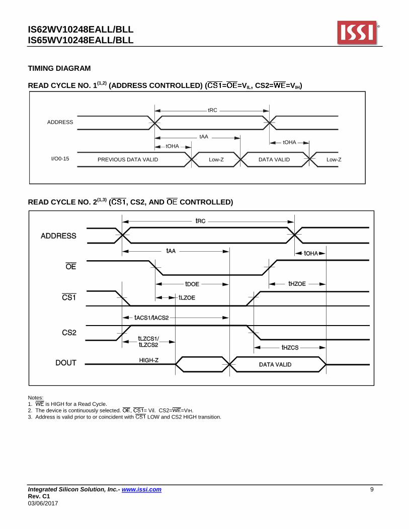
TIMING DIAGRAM
READ CYCLE NO. 1(1,2) (ADDRESS CONTROLLED) ( = =VIL, CS2= =VIH)
READ CYCLE NO. 2(1,3) ( , CS2, AND CONTROLLED)
Notes:
1. is HIGH for a Read Cycle.
2. The device is continuously selected. , = Vil. CS2= =VIH.
3. Address is valid prior to or coincident with LOW and CS2 HIGH transition.
tRC
ADDRESS
I/O0-15
tAA
tOHA tOHA
DATA VALID PREVIOUS DATA VALID Low-Z Low-Z

IS62WV10248EALL/BLL IS65WV10248EALL/BLL
Integrated Silicon Solution, Inc.- www.issi.com 10 Rev. C1
03/06/2017
WRITE CYCLE NO. 1 ( CONTROLLED, = HIGH OR LOW)
Notes:
1. tHZWE is based on the assumption when tSA=0nS after READ operation. Actual DOUT for tHZWE may not appear if goes high before
Write Cycle. tHZOE is the time DOUT goes to High-Z after goes high. 2. During this period the I/Os are in output state. Do not apply input signals.
WRITE CYCLE NO. 2 ( Controlled: is HIGH During Write Cycle)
Notes:
1. tHZWE is based on the assumption when tSA=0nS after READ operation. Actual DOUT for tHZWE may not appear if goes high before Write Cycle. tHZOE is the time DOUT goes to High-Z after goes high.
2. During this period the I/Os are in output state. Do not apply input signals

IS62WV10248EALL/BLL IS65WV10248EALL/BLL
Integrated Silicon Solution, Inc.- www.issi.com 11 Rev. C1
03/06/2017
WRITE CYCLE NO. 3 ( CONTROLLED: IS LOW DURING WRITE CYCLE)
Notes:
If is low during write cycle, tHZWE must be met in the application. Do not apply input signal during this period. Data output from the previous READ operation will drive IO BUS.
IS62WV10248EALL/BLL IS65WV10248EALL/BLL
Integrated Silicon Solution, Inc.- www.issi.com 12 Rev. C1
03/06/2017
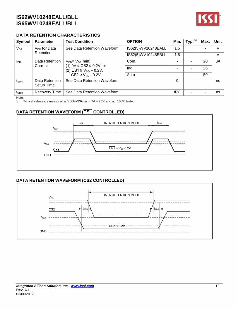
DATA RETENTION CHARACTERISTICS Symbol Parameter Test Condition OPTION Min. Typ.
(1) Max. Unit
VDR VDD for Data Retention
See Data Retention Waveform IS62(5)WV10248EALL 1.5 - V
IS62(5)WV10248EBLL 1.5 - V
IDR Data Retention Current
VDD= VDR(min), (1) 0V ≤ CS2 ≤ 0.2V, or
(2) ≥ VDD – 0.2V, CS2 ≥ VDD - 0.2V
Com. - - 20 uA
Ind. - - 25
Auto - - 50
tSDR Data Retention Setup Time
See Data Retention Waveform 0 - - ns
tRDR Recovery Time See Data Retention Waveform tRC - - ns
Note:
1. Typical values are measured at VDD=VDR(min), TA = 25 and not 100% tested.
DATA RETENTION WAVEFORM ( CONTROLLED)
DATA RETENTION WAVEFORM (CS2 CONTROLLED)
DATA RETENTION MODE tRDR tSDR
VDD
GND
VDR
> VDD-0.2V
DATA RETENTION MODE
tRDR tSDR
VDD
GND
VDR
CS2
CS2 < 0.2V
IS62WV10248EALL/BLL IS65WV10248EALL/BLL
Integrated Silicon Solution, Inc.- www.issi.com 13 Rev. C1
03/06/2017
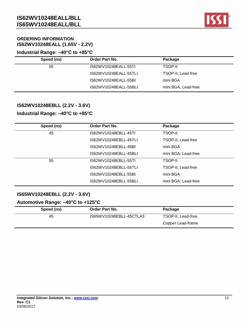
ORDERING INFORMATION
IS62WV10248EALL (1.65V - 2.2V)
Industrial Range: –40°C to +85°C
Speed (ns) Order Part No. Package
55 IS62WV10248EALL-55TI TSOP-II
IS62WV10248EALL-55TLI TSOP-II, Lead-free
IS62WV10248EALL-55BI mini BGA
IS62WV10248EALL-55BLI mini BGA, Lead-free
IS62WV10248EBLL (2.2V - 3.6V)
Industrial Range: –40°C to +85°C
Speed (ns) Order Part No. Package
45 IS62WV10248EBLL-45TI TSOP-II
IS62WV10248EBLL-45TLI TSOP-II, Lead-free
IS62WV10248EBLL-45BI mini BGA
IS62WV10248EBLL-45BLI mini BGA, Lead-free
55 IS62WV10248EBLL-55TI TSOP-II
IS62WV10248EBLL-55TLI TSOP-II, Lead-free
IS62WV10248EBLL-55BI mini BGA
IS62WV10248EBLL-55BLI mini BGA, Lead-free
IS65WV10248EBLL (2.2V - 3.6V)
Automotive Range: –40°C to +125°C
Speed (ns) Order Part No. Package
45 IS65WV10248EBLL-45CTLA3 TSOP-II, Lead-free,
Copper Lead-frame
IS62WV10248EALL/BLL IS65WV10248EALL/BLL
Integrated Silicon Solution, Inc.- www.issi.com 14 Rev. C1
03/06/2017
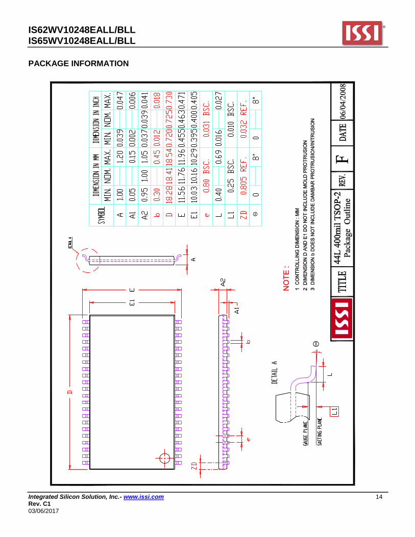
PACKAGE INFORMATION

IS62WV10248EALL/BLL IS65WV10248EALL/BLL
Integrated Silicon Solution, Inc.- www.issi.com 15 Rev. C1
03/06/2017
PACKAGE INFORMATION